EP2575164A2 - Structure de dispositif électronique intégré en 3D comprenant des capacités accrues de dissipation thermique - Google Patents
Structure de dispositif électronique intégré en 3D comprenant des capacités accrues de dissipation thermique Download PDFInfo
- Publication number
- EP2575164A2 EP2575164A2 EP12185346A EP12185346A EP2575164A2 EP 2575164 A2 EP2575164 A2 EP 2575164A2 EP 12185346 A EP12185346 A EP 12185346A EP 12185346 A EP12185346 A EP 12185346A EP 2575164 A2 EP2575164 A2 EP 2575164A2
- Authority
- EP
- European Patent Office
- Prior art keywords
- input
- substrate
- cap layer
- main surface
- output contacts
- Prior art date
- Legal status (The legal status is an assumption and is not a legal conclusion. Google has not performed a legal analysis and makes no representation as to the accuracy of the status listed.)
- Ceased
Links
Images
Classifications
-
- B—PERFORMING OPERATIONS; TRANSPORTING
- B81—MICROSTRUCTURAL TECHNOLOGY
- B81B—MICROSTRUCTURAL DEVICES OR SYSTEMS, e.g. MICROMECHANICAL DEVICES
- B81B3/00—Devices comprising flexible or deformable elements, e.g. comprising elastic tongues or membranes
- B81B3/0064—Constitution or structural means for improving or controlling the physical properties of a device
- B81B3/0081—Thermal properties
-
- B—PERFORMING OPERATIONS; TRANSPORTING
- B81—MICROSTRUCTURAL TECHNOLOGY
- B81C—PROCESSES OR APPARATUS SPECIALLY ADAPTED FOR THE MANUFACTURE OR TREATMENT OF MICROSTRUCTURAL DEVICES OR SYSTEMS
- B81C1/00—Manufacture or treatment of devices or systems in or on a substrate
- B81C1/00015—Manufacture or treatment of devices or systems in or on a substrate for manufacturing microsystems
- B81C1/00261—Processes for packaging MEMS devices
-
- B—PERFORMING OPERATIONS; TRANSPORTING
- B81—MICROSTRUCTURAL TECHNOLOGY
- B81B—MICROSTRUCTURAL DEVICES OR SYSTEMS, e.g. MICROMECHANICAL DEVICES
- B81B7/00—Microstructural systems; Auxiliary parts of microstructural devices or systems
- B81B7/0032—Packages or encapsulation
- B81B7/0077—Other packages not provided for in groups B81B7/0035 - B81B7/0074
-
- B—PERFORMING OPERATIONS; TRANSPORTING
- B81—MICROSTRUCTURAL TECHNOLOGY
- B81B—MICROSTRUCTURAL DEVICES OR SYSTEMS, e.g. MICROMECHANICAL DEVICES
- B81B7/00—Microstructural systems; Auxiliary parts of microstructural devices or systems
- B81B7/0083—Temperature control
- B81B7/009—Maintaining a constant temperature by heating or cooling
- B81B7/0093—Maintaining a constant temperature by heating or cooling by cooling
-
- H—ELECTRICITY
- H10—SEMICONDUCTOR DEVICES; ELECTRIC SOLID-STATE DEVICES NOT OTHERWISE PROVIDED FOR
- H10W—GENERIC PACKAGES, INTERCONNECTIONS, CONNECTORS OR OTHER CONSTRUCTIONAL DETAILS OF DEVICES COVERED BY CLASS H10
- H10W40/00—Arrangements for thermal protection or thermal control
- H10W40/20—Arrangements for cooling
- H10W40/22—Arrangements for cooling characterised by their shape, e.g. having conical or cylindrical projections
- H10W40/226—Arrangements for cooling characterised by their shape, e.g. having conical or cylindrical projections characterised by projecting parts, e.g. fins to increase surface area
- H10W40/228—Arrangements for cooling characterised by their shape, e.g. having conical or cylindrical projections characterised by projecting parts, e.g. fins to increase surface area the projecting parts being wire-shaped or pin-shaped
-
- H—ELECTRICITY
- H10—SEMICONDUCTOR DEVICES; ELECTRIC SOLID-STATE DEVICES NOT OTHERWISE PROVIDED FOR
- H10W—GENERIC PACKAGES, INTERCONNECTIONS, CONNECTORS OR OTHER CONSTRUCTIONAL DETAILS OF DEVICES COVERED BY CLASS H10
- H10W72/00—Interconnections or connectors in packages
- H10W72/01—Manufacture or treatment
- H10W72/0198—Manufacture or treatment batch processes
-
- H—ELECTRICITY
- H10—SEMICONDUCTOR DEVICES; ELECTRIC SOLID-STATE DEVICES NOT OTHERWISE PROVIDED FOR
- H10W—GENERIC PACKAGES, INTERCONNECTIONS, CONNECTORS OR OTHER CONSTRUCTIONAL DETAILS OF DEVICES COVERED BY CLASS H10
- H10W74/00—Encapsulations, e.g. protective coatings
- H10W74/01—Manufacture or treatment
-
- H—ELECTRICITY
- H10—SEMICONDUCTOR DEVICES; ELECTRIC SOLID-STATE DEVICES NOT OTHERWISE PROVIDED FOR
- H10W—GENERIC PACKAGES, INTERCONNECTIONS, CONNECTORS OR OTHER CONSTRUCTIONAL DETAILS OF DEVICES COVERED BY CLASS H10
- H10W76/00—Containers; Fillings or auxiliary members therefor; Seals
- H10W76/60—Seals
-
- H—ELECTRICITY
- H10—SEMICONDUCTOR DEVICES; ELECTRIC SOLID-STATE DEVICES NOT OTHERWISE PROVIDED FOR
- H10W—GENERIC PACKAGES, INTERCONNECTIONS, CONNECTORS OR OTHER CONSTRUCTIONAL DETAILS OF DEVICES COVERED BY CLASS H10
- H10W90/00—Package configurations
- H10W90/701—Package configurations characterised by the relative positions of pads or connectors relative to package parts
- H10W90/721—Package configurations characterised by the relative positions of pads or connectors relative to package parts of bump connectors
- H10W90/724—Package configurations characterised by the relative positions of pads or connectors relative to package parts of bump connectors between a chip and a stacked insulating package substrate, interposer or RDL
Definitions
- Embodiments presented herein relate to microelectronic device structures and, more particularly, to three-dimensional (3D) microelectronic integrated circuit (IC) chip structures including increased thermal dissipation capability.
- 3D three-dimensional microelectronic integrated circuit
- Microelectromechanical systems are miniaturized devices, such as microswitches that may range in size from less than 1 micron to about 1 mm or more.
- 3D integrated circuits in general, include two or more layers of electronic components in a stacked configuration that are integrated both vertically and horizontally. These devices generally require a controlled environment to operate for a long period of time. Dissipation of heat is a major issue in any high-power electronics or electrical application, and extremely important in high-powered microelectromechanical systems or MEMS devices.
- Through substrate vias referred to as TSVs, are utilized as conductors in the stack of chips, such as memory chips, providing amongst other functions, a heat path between the chips. Additional means for dissipating heat may be integrated.
- MEMS devices are interconnected using wirebonding.
- wirebonding can lead to severe limitations in the performance of the device.
- Limitations associated with wirebonding are related to the following factors, including, but not limited to, current handling capability of the wires and an insufficient thermal path that may particularly impact handling of short current surges.
- MEMS device may be interconnected using ribbon bonding with similar limitations in the performance of the device.
- an improved microelectronic chip structure including increased thermal management, such as improved heat dissipation paths, resulting in a more reliable high-performance device with increased current carrying capabilities may be desired.
- it may provide protection from contaminants to an active device.
- an apparatus including a three-dimensional (3D) integrated chip assembly and a substrate, wherein the three-dimensional (3D) integrated chip assembly is flip chip bonded to a substrate, and wherein a plurality of heat dissipation paths extend through the three-dimensional (3D) integrated chip assembly to dissipate heat generated therein.
- the chip assembly including a device substrate; an active device comprising one or more heat generating elements disposed on the device substrate; a cap layer physically bonded to the device substrate; and a hermetic seal formed about the active device, the hermetic seal at least partially defined by the device substrate and the cap layer.
- an apparatus including a three-dimensional (3D) integrated chip assembly, a substrate and a heat spreader positioned proximate the three-dimensional (3D) integrated chip assembly via a thermal interface material (TIM).
- the three-dimensional (3D) integrated chip assembly is flip chip bonded to the substrate.
- the apparatus provides a plurality of heat dissipation paths through the three-dimensional (3D) integrated chip assembly to dissipate heat generated within the apparatus.
- the chip assembly including a device substrate; an active device comprising one or more integrated circuits disposed on the device substrate; a cap layer comprising a semiconductor material, the cap layer physically bonded to the device substrate; a hermetic seal formed about the active device, the hermetic seal at least partially defined by the device substrate and the cap layer.
- an apparatus including a MEMS device including a cap layer and a hermetic seal, at least partially defined by the cap layer, and a substrate.
- the MEMS device is configured to be flip chip bonded to the substrate.
- a method of dissipating heat within an apparatus including providing a three-dimensional (3D) integrated chip assembly.
- the method of providing the chip assembly including providing a device substrate having a first main surface and a second main surface, disposing an active device comprising one or more integrated circuits on the device substrate, bonding a cap layer to the device substrate, forming a hermetic seal about the active device and providing a substrate including a plurality of input/output connections.
- the device substrate including a plurality of input/output connections on at least one of the first main surface and the second main surface.
- the cap layer having a first main surface and a second main surface and including a plurality of input/output connections on at least one of the first main surface and the second main surface.
- the hermetic seal at least partially defined by the device substrate and the cap layer.
- the method further provides flip chip bonding the three-dimensional (3D) integrated chip assembly to the substrate to form an apparatus, wherein the apparatus provides a plurality of heat dissipation paths through the three-dimensional (3D) integrated chip assembly to dissipate heat generated within the apparatus.
- top and bottom are not used here because parts of the assembly are processed partly in one orientation, and partly in another. Instead, the terms “first surface” and “second surface” are used, such that all of the first surfaces eventually face the same direction in the finished device structure and all second surfaces eventually face the same direction in the finished device structure.
- the 3D integrated device assembly includes integrated layers and parallel connected interconnects to aid in efficient thermal dissipation of heat generated within the device structure and provide increased current carrying capabilities, while lowering electrical resistance in the interconnect structures.
- MEMS microelectromechanical systems
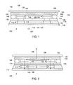
- FIG. 1 illustrated is a cross-sectional embodiment of one example of a device structure employing a 3D integrated chip assembly with increased thermal dissipation capabilities.
- This device structure generally denoted 100, includes a 3D integrated chip assembly 105 mounted to a substrate 110 having a first main surface 111 and a second main surface 112.
- the 3D integrated chip assembly 105 in general comprises a cap layer 114 having a first main surface 122 and a second main surface 124 and a device substrate 132 having a first main surface 140 and a second main surface 150.
- the 3D integrated chip assembly 105 is mounted to the second main surface 112 of the substrate 110.
- the cap layer 114 is mounted via a first main surface 122 to the substrate 110 utilizing a plurality of micro-bump connections 115, also referred to herein as flip chip bump bonding, that allow for high current carrying capabilities.
- the device substrate 132 is mounted onto a second main surface 124 of the cap layer 114, via a first main surface 140 of the device substrate 132 via standard metal interconnects (described presently).
- a heat spreader 152 may be positioned on a second main surface 150 of the device substrate 132 via a thermal interface material (TIM) 154.
- TIM thermal interface material
- the substrate 110 for electrical interconnection may be a printed circuit board (PCB) well known in the art.
- the substrate material in an alternative embodiment may comprise an active device layer, such as a metal-oxide semiconductor (MOS) based layer, including, silicon, silicon carbide, gallium-arsenide, etc., or when not considered an active layer, may be comprised of any flat supportive material, such as a polished metal, a flexible plastic, polyimide, a semiconductor material, or an insulator such as glass or a quartz material.
- MOS metal-oxide semiconductor
- the device substrate 132 may be formed of silicon well known in the art.
- the device substrate material in an alternative embodiment may comprise any flat supportive material compatible with semiconductor and MEMS based fabrication and packaging processes, such as silicon, silicon carbide, gallium arsenide, gallium nitride, alumina, sapphire, titanium, steel, plastics, polyimide, glass, quartz etc.
- the second main surface 112 of the substrate 110 contains a plurality of input/output contacts 116 which are shown soldered via a plurality of parallel configured solder bumps 118 to a plurality of first input/output contacts 120 disposed on the first main surface 122 of the cap layer 114 and configured to match the input/output contacts 116 of the substrate 110.
- Standard wafer processes are used to fabricate the substrate 110 layer's plurality of input/output contacts 116, patterned and located to match the input/output contacts of a cap layer 114 (described presently) to which the 3D integrated chip assembly 105, and more particularly the cap layer 114, is to be attached.
- the plurality of input/output contacts 116 could be constructed as one or more metal layers, e.g., copper, nickel and/or gold layers. The actual composition of the metal layers in the input/output contact stacks would be dependent on the substrate 110 materials.
- the device substrate 132 and cap layer 114 are first bonded together to form the 3D integrated chip assembly 105, also referred to herein as a "MEMS" or “device chip", that is then attached via solder bumps 118 to the substrate 110.
- MEMS 3D integrated chip assembly 105
- solder bumps 118 solder bumps 118 to the substrate 110.
- many parallel bumps are used to serve as high current carriers as well as thermal shunts.
- the parallel microbump interconnections can range from 2 to 50 or even more in number per IO depending on the package size, IO count, etc.
- An underfill material 121 is illustrated as disposed between the substrate 110 and the cap layer 114.
- the underfill material 121 can be used to fill in the space between the substrate 110 and the cap layer 114 so that the micro-bump connections 115, and more particularly the plurality of input/output connections 116, the plurality of first input/output connections 120 and the solder bumps 118 remain secured.
- they may expand or contract by different amounts when the device structure 100 is heated or cooled due to the heat generated during operation. This heating or cooling of the device structure 100 may create relative motion between the various device structure 100 layers.
- the inclusion of the underfill material 121 may aid in preventing the interconnects between the substrate 110 and the cap layer 114 becoming unsecured.
- the cap layer 114 is further configured to support on the second main surface 124, a plurality of second input/output contacts 126 configured to match, or otherwise interface to or be compatible with, a plurality of input/output contacts (described presently) formed on the device substrate 132.
- Interconnects from the lower main surface 122 of the cap layer 114 to the second main surface 124 can be achieved by various means, including constructing a plurality of through substrate vias 130, and more particularly a plurality of through silicon vias (TSVs) 130, constructed using, for example, laser, high rate reactive ion etching, etc., for via formation and standard wafer processes for via metallization.
- TSVs through silicon vias
- the plurality of first input/output contacts 120 electrically connect via the plurality of through wafer vias 128 to the plurality of second input/output contacts 126 disposed on the second main surface 124 of the cap layer 114.
- the plurality of through wafer vias 128 are electrically isolated from the cap layer 114.
- One embodiment of the device 100 described herein includes the fabrication of the cap layer 114 of a semiconductor material, and for example, matching the cap layer 114 material to the substrate 110 to which it is to be connected, when the substrate 110 is not a printed circuit board (PCB). More specifically, one method of fabricating the device structure 100 is to select the cap layer 114 of a semiconductor material to match the material employed by the substrate 110; for example, silicon. This minimizes mechanical stress, strain and otherwise provides a high reliability package and interconnects, and also provides for an electrical interconnect performance equivalent. By way of example, if the device structure 100 includes a silicon substrate 110 then the cap layer 114 may also be fabricated of silicon. Since silicon based integrated circuit devices predominate today, the discussion provided herein may discuss a silicon cap layer 114.
- the device substrate material and the cap layer material could comprise any semiconductor material, including, silicon, silicon carbide, gallium-arsenide, etc. or alternatively a material such as quartz, or the like.
- Standard wafer processes can be employed to fabricate the cap layer 114, including creating the plurality of first input/output contacts 120 on the cap layer 114 using wafer processing.
- the plurality of through wafer vias 128 are created (by, for example, plasma etching, drilling, laser drilling, chemical etching, high rate reactive ion etching, laser ablation, etc., through the cap layer 114), optionally insulated to electrically isolate the cap layer 114 and subsequent electrical interconnections, and then metalized to form electrical connections from the first main surface 122 of the cap layer 114 to the second main surface 124 of the cap layer 114.
- metalized through wafer vias 128 can be employed to create the metalized through wafer vias 128.
- One embodiment of the through-via construction process is to use wet chemistry (to relieve stress) followed by oxidation to establish an insulative layer partially covering the surface of the cap layer 114 and the walls of the vias (without filling the vias) to provide the necessary electrical isolation from the cap layer 114. Seed metal is then deposited to establish a metal layer in the vias, prior to plating the vias with metal, for example, copper, nickel, gold, etc.
- a photomask is applied and the circuitry (e.g., input/output) contacts and interconnect to the through vias, if any, is patterned.
- the circuitry e.g., input/output
- cap layer 114 such as depicted in FIG. 1 is attained, wherein the metalized through vias extend from the first main surface 122 to the second main surface 124 of the cap layer 114.
- the cap layer's 114 plurality of input/output contacts 126 are used to fabricate the cap layer's 114 plurality of input/output contacts 126, patterned and located to match the input/output contacts of a device substrate 132 to which the cap layer 114 is to be attached, in addition to fabricating the plurality of first input/output contacts 120.
- the plurality of input/output contacts 120 are formed on the opposite first main surface 122 of the cap layer 114.
- the pluralities of input/output contacts 120 and 126 could be constructed as a stack of metal layers, e.g., copper, nickel and/or gold layers. The actual composition of the metal layers in the input/output contact stacks would be dependent on the cap layer 114 material and attachment method used.
- the plurality of through wafer vias 128 formed within the cap layer 114 are aligned under or in close proximity to the plurality of first input/output contacts 120 to be disposed on the first main surface 122 of the cap layer 114 and the plurality of second input/output contacts 126 to be disposed on the second main surface 124 of the cap layer 114.
- the plurality of second input/output contacts 126 in one embodiment, are patterned to match a plurality of input/output contacts 138 or pad configuration of the device substrate 132 to which the cap layer 114 is to be attached, while the plurality of second input/output contacts 120 are configured to facilitate connection to the substrate 110 which the cap layer 114 is also to be connected.
- the diameters of the through wafer vias 128 are dependent on the quantity of through wafer vias 128 and location of the device substrate 132, plurality of input/output contacts 138 and plurality of input/output contacts 116.
- the diameter of each via 128 may be as small as ten microns or less using today's technology.
- the plurality of first input/output contacts 120 disposed on the first main surface 122 of the cap layer 114 electrically connect via metalized vias 128 to the plurality of second input/output contacts 126 disposed on the second main surface 124 of the cap layer 114.
- the device substrate 132 includes a plurality of input/output contacts 138 formed on the first main surface 140.
- the plurality of input/output contacts 138 are shown bonded, such as through thermocompression bonding, to the plurality of second input/output contacts 126 disposed on the second main surface 124 of the cap layer 114 and configured to match the input/output contacts 126 of the cap layer 114.
- Thermally conductive traces 143 provide for interconnect of an active device to the first main surface 140 of the device substrate 132 and dissipation of heat (described presently).
- active device may comprise any heat generating element, such as a semiconducting integrated circuit (IC), a simple resistor, a sensor such as an acoustic (ultrasound) sensor, an optical (LCD, photodiode, spatial light modulator) device, or any similar type heat generating device.
- the active device 144 comprises a microelectromechanical system (MEMS) circuit and in particular a micro scale relay.
- MEMS microelectromechanical system
- a sealing ring 146 provides hermetic sealing of the active device 144.
- the sealing ring 146 may be comprised of any known sealing material, such as glass frit, eutectic metal compositions, polymer adhesives, thermal compressive metal bonds, or the like.
- a glass frit ring such as a thixotropic paste, may be screen printed onto one of the device substrate 132 or the cap layer 114 and dried.
- the frit thickness is in the 5 to 20 micron range. The printed glass frit ring will eventually form a hermetic seal 148 for the individual active device(s) 144.
- a wafer bonding process to melt the glass particles, is performed thereby creating the sealing ring 146 and the hermetic seal 148.
- Typical wafer processing of the glass frit ring may employ glass reflow and bonding temperatures of approximately 400 °C under vacuum and with an applied wafer-to-wafer force.
- the reflowed glass frit sealing process will permit the sealing ring 146 to hermetically seal the active device 144 between the second main surface 124 of the cap layer 114 and the first main surface 140 of the device substrate 132. Due to the movement generated by the mechanical components during operation, the active device 144 is susceptible to external air and unwanted particles, such as moisture, dust particles, or the like.
- the sealing ring 146 and hermetic seal 148 about the active device 144 may provide protection from these unwanted contaminants.
- a second main surface 150 of the device substrate 132 may be attached to an optional heat spreader 152, via a thermal interface material (TIM) 154 disposed therebetween.
- TIM thermal interface material
- heat generated by the active device 144 may be dissipated through the heat spreader 152 into the external environment.
- the inclusion of the heat spreader 152 and the TIM 154 may be dependent upon the need for additional heat dissipation capabilities within the structure 100.
- the cap layer 114, hermetic sealing of the active device 144, plurality of parallel interconnects and overall device structure 100 constructed as discussed above may alleviate some or all of the problems associated with heat dissipation in high powered microelectronic chip structures, and more particularly high powered microelectromechanical systems (MEMS).
- MEMS microelectromechanical systems
- the 3D integrated chip assembly 105 constructed as described herein can be easily picked and placed with a high-accuracy, high volume placement machine and assembled onto the substrate 110 for packaging.
- FIG. 2 illustrated is the device structure 100, constructed according to the previous description, depicting a plurality of heat dissipation paths 156 according to an embodiment.
- like numerals refer to like elements throughout the several views.
- the heat dissipation paths 156 as disclosed herein place the heat generation in direct connection with dissipation over the power lines compared to heat spreaders which require heat to first flow through the bulk substrate, then through the TIM and then to the heat spreader.
- heat generated by the device structure 100, and more particularly the active device 144 is dissipated via the plurality of heat dissipation paths 156, and in particular along thermally conductive traces 143 on the wafer or cap surface that take heat from the device 144 to the interconnect structure 125 and down the solder bump flip chip assembly 115.
- the heat dissipation paths 156 provide a continuous thermally conductive metal pathway from the active device 144 to its metal interconnections, thus serving as the primary path for heat dissipation.
- the flip chip interconnects 115 provide many thermal dissipation paths 156 through each electrical joint that are better thermally coupled to the heat generation source, and more particularly the active device 144, than solely relying on heat dissipation through bulk silicon, or the like. In addition to providing for many parallel shorter electrical paths 156, the flip chip interconnects 115 provide for shorter dissipation paths 156. As depicted, heat may be dissipated by the microbump interconnects 115 formed by the flip chip joints located between the substrate 110 and the cap layer 114, and the metal interconnections 125 formed between the cap layer 114 and the device substrate 132. Any additional heat may be dissipated through the heat spreader 152, when included in the device structure 100. The described novel flip chip approach provides for a shorter interconnect path length, thereby making it more favorable to dissipate heat. Such short and highly parallelized thermal paths serve a significant advantage over other interconnection methods such as wire-bonds and ribbon bonding.
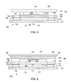
- FIG. 3 illustrated is another embodiment of a device structure 200 including a substrate 110, and a 3D integrated chip assembly 105 generally comprising a cap layer 114 and a device substrate 132.
- the device substrate 132 is disposed in a lower portion of the 3D integrated chip assembly 105 and more particularly, the cap layer 114 is disposed on a first main surface 150 of the device substrate 132.
- the active device 144 is positioned via thermally conductive traces 143 on the second main surface 150 of the device substrate 132.
- the device substrate 132 further includes a plurality of through wafer vias 130 formed therein and a plurality of first input/output contacts 120 disposed over a first main surface 140 thereof, wherein the plurality of second input/output contacts 120 are electrically connected to the active device 144 through the plurality of through wafer vias 130.
- flip chip bump interconnects to those of the first embodiment illustrated in FIGs. 1 and 2 are formed between a second main surface 112 of the substrate 110 and the first main surface 140 of the device substrate 132.
- An underfill material 121 may be provided.
- the sealing ring 146 forms a hermetic seal 148 for the active device 144 between the device substrate 132 and the cap layer 114.
- the sealing ring 146 provides a physical bond between the second main surface 150 of the device substrate 132 and the first main surface 122 of the cap layer 114.
- the heat spreader 152 and the thermal interface material 154 have been omitted. Similar to the first disclosed embodiment, heat generated by the device structure 200, and more particularly the active device 144, is dissipated in a similar manner according to heat dissipation paths illustrated in FIG. 2 .
- FIG. 4 illustrated is yet another embodiment of a device structure 300 including a substrate 110 and a 3D integrated chip assembly 105 generally comprising a cap layer 114 and a device substrate 132, configured in a stack generally similar to the embodiment described in FIGs. 1 and 2 .
- the heat spreader 152 and the thermal interface material 154 have been omitted.
- An optional heat spreader 152 is positioned on the first main surface 124 of the cap layer 114 via a thermal interface material (TIM) 154.
- TIM thermal interface material
- the sealing ring is omitted, and a hermetic seal 148 for the active device 144 is formed by the device substrate 132, the cap layer 114, and the metal interconnects 125 formed between the cap layer 114 and the device substrate 132. More specifically, the plurality of second input/output contacts 126 formed on the second main surface 124 of the cap layer 114 and the plurality of input/output contacts 138 formed on the first main surface 140 of the device substrate 132, provide for the hermetic seal 148 about the active device 144.
- an additional interconnect-via structure can be included about the active device 144, comprising a set of metal interconnects 125 formed between the cap layer 114 and the device substrate 132, vias 130, and interconnects 116, 120 and bumps 118 formed between the cap layer 114 and the substrate 110 may be included to form an additional seal.
- heat generated by the device structure 300, and more particularly the active device 144 is dissipated in a similar manner according to heat dissipation paths illustrated in FIG. 2 .
- FIG. 4 includes the 3D integrated chip assembly 105 configured wherein the cap layer 114 is positioned to allow for attachment to the substrate 110
- the cap layer 114 and device substrate 132 may be reversed with respect to configuration in the 3D integrated chip assembly 105, such as described and illustrated in FIG. 3 , to allow for attachment of the device substrate 132 to the substrate 110.
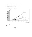
- FIG. 5 Illustrated in FIG. 5 , are simulation results 400 depicting heat dissipation of embodiments of a high powered microelectronic device structure including known interconnect/stack configurations and the novel interconnect/stack configurations described herein. More specifically, heat dissipation is graphically represented in FIG. 5 to illustrate the improved heat dissipation qualities of a flip chip board configuration.
- Current (A) is represented on an x-axis 402 the maximum temperature in the package (typically at the MEMS beams) and temperature (K) is represented on a y-axis 403.
- Typical heat dissipation in a known microelectronic device structure, including standard wire bond/trace interconnects and a heat spreader is depicted at line 404. As indicated, at a current of approximately 30 Amps, wire bond/trace interconnects limit the thermal conductivity of the packaged device causing the temperature to get excessively hot, and as illustrated in excess of 700 K.
- Typical heat dissipation of a known microelectronic device structure including copper strap interconnects and a heat spreader is depicted at line 406. As indicated, at a current of approximately 30 Amps the heat in a known device including copper strap interconnects, while capable of dissipating heat more efficiently than in the previous device including wire bond/trace interconnects, is only capable of dissipating heat wherein the device remains at a temperature in excess of 460 K.
- Typical heat dissipation of a microelectronic device structures configured to include a cap layer, hermetic seal and interconnects as in the previously described embodiments of FIG. 1-4 are depicted at lines 408 and 410.
- line 408 at a current of approximately 30 Amps the heat in a novel device including a cap layer, hermetic seal, novel flip chip interconnects and a heat spreader, such as that described in FIGs. 1-4 is capable of dissipating heat more efficiently than in previous known devices including wire bond/trace interconnects or ribbon-based interconnects.
- the temperature is efficiently dissipated and the temperature of the device at approximately 30Amps is less than 400 K.
- Typical heat dissipation of a microelectronic device structure configured to include a cap layer, hermetic seal and interconnects as in the previously described embodiment of FIG. 4 , wherein a heat spreader is not incorporated in the device structure is depicted at line 410.
- line 410 at a current of approximately 30 Amps the heat in a novel device including a cap layer and novel flip chip interconnects, but without the inclusion of a heat spreader, while dissipating less heat than the flip chip embodiment incorporating the heat spreader at line 408, remains capable of dissipating heat more efficiently than in previous known devices including wire bond/trace interconnects or copper strap interconnects wherein a heat spreader was utilized.
- the temperature in this embodiment is efficiently dissipated and the temperature of the device at approximately 30Amps is less than 450 K.
- a novel interconnect structure and device structure stack or package which can be employed to improve heat dissipation in high power microelectronic devices, such as microelectromechanical systems (MEMS) devices.
- MEMS microelectromechanical systems
- fabricating the device to include a 3D integrated chip assembly comprising a cap layer, a device substrate, a plurality of metal interconnects and an active device, a plurality of bump interconnects between the 3D integrated chip assembly and an underlying substrate and a hermetic seal about the active device and between the cap layer and the device substrate, a low cost, high performance, high yield device structure can be obtained using standard chemistry, mechanical processes, etc.
- the device structure and techniques disclosed herein may result in advantages including, but not limited to, increased thermal management by way of increased heat dissipation capabilities, easier package integration and lower electrical resistance interconnects.
- Mechanical and thermal management systems for rather thin, fragile integrated circuit chips and devices are also provided.
Landscapes
- Engineering & Computer Science (AREA)
- Microelectronics & Electronic Packaging (AREA)
- Computer Hardware Design (AREA)
- Manufacturing & Machinery (AREA)
- Physics & Mathematics (AREA)
- Thermal Sciences (AREA)
- Cooling Or The Like Of Semiconductors Or Solid State Devices (AREA)
- Micromachines (AREA)
Applications Claiming Priority (1)
| Application Number | Priority Date | Filing Date | Title |
|---|---|---|---|
| US13/249,492 US8698258B2 (en) | 2011-09-30 | 2011-09-30 | 3D integrated electronic device structure including increased thermal dissipation capabilities |
Publications (2)
| Publication Number | Publication Date |
|---|---|
| EP2575164A2 true EP2575164A2 (fr) | 2013-04-03 |
| EP2575164A3 EP2575164A3 (fr) | 2016-01-13 |
Family
ID=47221939
Family Applications (1)
| Application Number | Title | Priority Date | Filing Date |
|---|---|---|---|
| EP12185346.9A Ceased EP2575164A3 (fr) | 2011-09-30 | 2012-09-21 | Structure de dispositif électronique intégré en 3D comprenant des capacités accrues de dissipation thermique |
Country Status (4)
| Country | Link |
|---|---|
| US (2) | US8698258B2 (fr) |
| EP (1) | EP2575164A3 (fr) |
| JP (1) | JP6416454B2 (fr) |
| CN (1) | CN103030093B (fr) |
Cited By (2)
| Publication number | Priority date | Publication date | Assignee | Title |
|---|---|---|---|---|
| US9851398B2 (en) | 2015-03-30 | 2017-12-26 | Globalfoundries Inc. | Via leakage and breakdown testing |
| CN116675175A (zh) * | 2023-08-04 | 2023-09-01 | 青岛泰睿思微电子有限公司 | 一种多功能影像光感封装设备 |
Families Citing this family (19)
| Publication number | Priority date | Publication date | Assignee | Title |
|---|---|---|---|---|
| BR9402301A (pt) | 1994-07-22 | 1996-04-30 | Rheem Ind Comerc Sa | Corpo de lata com sistema de proteçao anti-corte e processo de abtençao de um corpo de lata com sistema de proteçao anti-corte |
| US9006889B2 (en) | 2011-11-11 | 2015-04-14 | Skyworks Solutions, Inc. | Flip chip packages with improved thermal performance |
| JP6150249B2 (ja) * | 2013-02-25 | 2017-06-21 | 京セラ株式会社 | 電子デバイスのガラス封止方法 |
| US9123686B2 (en) * | 2013-04-12 | 2015-09-01 | Western Digital Technologies, Inc. | Thermal management for solid-state drive |
| US9823539B2 (en) | 2013-06-26 | 2017-11-21 | Empire Technology Development Llc | Methods and systems for forming optical modulators using micro-contact lithography |
| KR102066015B1 (ko) | 2013-08-13 | 2020-01-14 | 삼성전자주식회사 | 반도체 패키지 및 이의 제조방법 |
| WO2015105849A1 (fr) * | 2014-01-08 | 2015-07-16 | Enphase Energy, Inc. | Dissipateur thermique double et isolé |
| US9611137B2 (en) * | 2014-08-26 | 2017-04-04 | Invensense, Inc. | MEMS sensor integrated with a flip chip |
| JP6019367B2 (ja) * | 2015-01-13 | 2016-11-02 | 株式会社野田スクリーン | 半導体装置 |
| US10107662B2 (en) | 2015-01-30 | 2018-10-23 | Honeywell International Inc. | Sensor assembly |
| JP6341190B2 (ja) * | 2015-02-16 | 2018-06-13 | 株式会社デンソー | 半導体装置の製造方法 |
| CN105990271B (zh) | 2015-02-26 | 2020-06-05 | 恩智浦美国有限公司 | 具有非水平管芯垫及相应引线框的ic封装 |
| US9548255B1 (en) | 2015-08-17 | 2017-01-17 | Freescale Semiconductor, Inc. | IC package having non-horizontal die pad and flexible substrate therefor |
| TW201735286A (zh) | 2016-02-11 | 2017-10-01 | 天工方案公司 | 使用可回收載體基板之裝置封裝 |
| US20170243739A1 (en) * | 2016-02-24 | 2017-08-24 | Skyworks Solutions, Inc. | 3d micromold and pattern transfer |
| US10453763B2 (en) | 2016-08-10 | 2019-10-22 | Skyworks Solutions, Inc. | Packaging structures with improved adhesion and strength |
| DE102017204817B4 (de) | 2017-03-22 | 2019-03-21 | Infineon Technologies Ag | Vorrichtung mit Hohlraumstruktur und Verfahren zum Herstellen selbiger |
| DE102017012256B3 (de) * | 2017-03-22 | 2021-05-20 | Infineon Technologies Ag | Vorrichtung mit Hohlraumstruktur und Verfahren zum Herstellen selbiger |
| CN113044802A (zh) * | 2021-04-13 | 2021-06-29 | 北京航空航天大学 | Mems器件真空封装结构及其制造工艺 |
Citations (2)
| Publication number | Priority date | Publication date | Assignee | Title |
|---|---|---|---|---|
| WO2002055431A2 (fr) * | 2001-01-10 | 2002-07-18 | Raytheon Company | Interconnexion au niveau plaquette |
| US20040264152A1 (en) * | 2003-06-25 | 2004-12-30 | Heck John M. | MEMS RF switch module including a vertical via |
Family Cites Families (30)
| Publication number | Priority date | Publication date | Assignee | Title |
|---|---|---|---|---|
| JPS5040941Y1 (fr) * | 1970-06-08 | 1975-11-21 | ||
| JPH09148499A (ja) * | 1995-11-29 | 1997-06-06 | Miyazaki Oki Electric Co Ltd | 半導体気密封止型パッケージ及びその製造方法 |
| JP3846094B2 (ja) * | 1998-03-17 | 2006-11-15 | 株式会社デンソー | 半導体装置の製造方法 |
| JP2001053178A (ja) * | 1999-06-02 | 2001-02-23 | Japan Radio Co Ltd | 電子回路装置が封止され回路基板に実装される電子部品及びその製造方法 |
| US6949880B1 (en) * | 1999-12-17 | 2005-09-27 | Osram Opto Semiconductors Gmbh | Encapsulation for organic LED device |
| US6384353B1 (en) * | 2000-02-01 | 2002-05-07 | Motorola, Inc. | Micro-electromechanical system device |
| US6441481B1 (en) * | 2000-04-10 | 2002-08-27 | Analog Devices, Inc. | Hermetically sealed microstructure package |
| US6624921B1 (en) * | 2001-03-12 | 2003-09-23 | Amkor Technology, Inc. | Micromirror device package fabrication method |
| KR100387239B1 (ko) * | 2001-04-26 | 2003-06-12 | 삼성전자주식회사 | Mems 릴레이 및 그 제조방법 |
| US6815739B2 (en) | 2001-05-18 | 2004-11-09 | Corporation For National Research Initiatives | Radio frequency microelectromechanical systems (MEMS) devices on low-temperature co-fired ceramic (LTCC) substrates |
| US6559530B2 (en) * | 2001-09-19 | 2003-05-06 | Raytheon Company | Method of integrating MEMS device with low-resistivity silicon substrates |
| US6673697B2 (en) * | 2002-04-03 | 2004-01-06 | Intel Corporation | Packaging microelectromechanical structures |
| US6696645B2 (en) * | 2002-05-08 | 2004-02-24 | The Regents Of The University Of Michigan | On-wafer packaging for RF-MEMS |
| SG111972A1 (en) * | 2002-10-17 | 2005-06-29 | Agency Science Tech & Res | Wafer-level package for micro-electro-mechanical systems |
| JP4342174B2 (ja) * | 2002-12-27 | 2009-10-14 | 新光電気工業株式会社 | 電子デバイス及びその製造方法 |
| JP2005019966A (ja) * | 2003-06-06 | 2005-01-20 | Sanyo Electric Co Ltd | 半導体装置及びその製造方法 |
| JP4268480B2 (ja) * | 2003-08-27 | 2009-05-27 | 京セラ株式会社 | 電子部品封止用基板およびそれを用いた電子装置 |
| US7030642B2 (en) * | 2004-02-06 | 2006-04-18 | Honeywell International Inc. | Quick attachment fixture and power card for diode-based light devices |
| US7312505B2 (en) * | 2004-03-31 | 2007-12-25 | Intel Corporation | Semiconductor substrate with interconnections and embedded circuit elements |
| US7262509B2 (en) * | 2004-05-11 | 2007-08-28 | Intel Corporation | Microelectronic assembly having a perimeter around a MEMS device |
| US7204737B2 (en) * | 2004-09-23 | 2007-04-17 | Temic Automotive Of North America, Inc. | Hermetically sealed microdevice with getter shield |
| US7791183B1 (en) * | 2005-04-11 | 2010-09-07 | The United States Of America As Represented By The Secretary Of The Air Force | Universal low cost MEM package |
| US7897503B2 (en) | 2005-05-12 | 2011-03-01 | The Board Of Trustees Of The University Of Arkansas | Infinitely stackable interconnect device and method |
| US7491567B2 (en) * | 2005-11-22 | 2009-02-17 | Honeywell International Inc. | MEMS device packaging methods |
| US20070114643A1 (en) * | 2005-11-22 | 2007-05-24 | Honeywell International Inc. | Mems flip-chip packaging |
| US7936062B2 (en) * | 2006-01-23 | 2011-05-03 | Tessera Technologies Ireland Limited | Wafer level chip packaging |
| US7642657B2 (en) * | 2006-12-21 | 2010-01-05 | Analog Devices, Inc. | Stacked MEMS device |
| US7723144B2 (en) * | 2007-03-02 | 2010-05-25 | Miradia Inc. | Method and system for flip chip packaging of micro-mirror devices |
| US8604603B2 (en) | 2009-02-20 | 2013-12-10 | The Hong Kong University Of Science And Technology | Apparatus having thermal-enhanced and cost-effective 3D IC integration structure with through silicon via interposers |
| CN101959106A (zh) * | 2009-07-16 | 2011-01-26 | 鸿富锦精密工业(深圳)有限公司 | 微机电系统麦克风的封装结构及其封装方法 |
-
2011
- 2011-09-30 US US13/249,492 patent/US8698258B2/en active Active
-
2012
- 2012-09-21 EP EP12185346.9A patent/EP2575164A3/fr not_active Ceased
- 2012-09-25 JP JP2012210260A patent/JP6416454B2/ja active Active
- 2012-10-08 CN CN201210376998.6A patent/CN103030093B/zh active Active
-
2014
- 2014-02-21 US US14/186,362 patent/US8802475B2/en active Active
Patent Citations (2)
| Publication number | Priority date | Publication date | Assignee | Title |
|---|---|---|---|---|
| WO2002055431A2 (fr) * | 2001-01-10 | 2002-07-18 | Raytheon Company | Interconnexion au niveau plaquette |
| US20040264152A1 (en) * | 2003-06-25 | 2004-12-30 | Heck John M. | MEMS RF switch module including a vertical via |
Cited By (3)
| Publication number | Priority date | Publication date | Assignee | Title |
|---|---|---|---|---|
| US9851398B2 (en) | 2015-03-30 | 2017-12-26 | Globalfoundries Inc. | Via leakage and breakdown testing |
| CN116675175A (zh) * | 2023-08-04 | 2023-09-01 | 青岛泰睿思微电子有限公司 | 一种多功能影像光感封装设备 |
| CN116675175B (zh) * | 2023-08-04 | 2023-12-08 | 青岛泰睿思微电子有限公司 | 一种多功能影像光感封装结构 |
Also Published As
| Publication number | Publication date |
|---|---|
| EP2575164A3 (fr) | 2016-01-13 |
| US8802475B2 (en) | 2014-08-12 |
| CN103030093B (zh) | 2018-02-02 |
| JP2013080923A (ja) | 2013-05-02 |
| JP6416454B2 (ja) | 2018-10-31 |
| US8698258B2 (en) | 2014-04-15 |
| CN103030093A (zh) | 2013-04-10 |
| US20140170811A1 (en) | 2014-06-19 |
| US20130082376A1 (en) | 2013-04-04 |
Similar Documents
| Publication | Publication Date | Title |
|---|---|---|
| US8802475B2 (en) | Method of fabricating a 3D integrated electronic device structure including increased thermal dissipation capabilities | |
| CN107799499B (zh) | 半导体封装结构及其制造方法 | |
| US8362607B2 (en) | Integrated circuit package including a thermally and electrically conductive package lid | |
| CN104733329B (zh) | 半导体封装结构和工艺 | |
| JP5568205B2 (ja) | インタポーザ、インタポーザパッケージ、及びそれらを使用したデバイス組立体 | |
| US7573139B2 (en) | Packed system of semiconductor chips having a semiconductor interposer | |
| CN103187377B (zh) | 具有桥型中介片的半导体封装 | |
| CN103633075B (zh) | 叠层封装半导体器件 | |
| KR101678539B1 (ko) | 적층 패키지, 반도체 패키지 및 적층 패키지의 제조 방법 | |
| CN103378017B (zh) | 高密度3d封装 | |
| US20140264808A1 (en) | Chip arrangements, chip packages, and a method for manufacturing a chip arrangement | |
| US20090014856A1 (en) | Microbump seal | |
| CN107845628A (zh) | 集成电路器件及其组装方法 | |
| CN107408515A (zh) | 具有用于晶片与晶片互连的桥接模块的半导体组件 | |
| CN107039366A (zh) | 半导体器件结构及其形成方法 | |
| US8546187B2 (en) | Electronic part and method of manufacturing the same | |
| CN106298549B (zh) | 倒装芯片封装 | |
| KR101053746B1 (ko) | 반도체 시스템 및 그 제조 방법 | |
| CN119447055A (zh) | 具有用于高效散热的热焊盘的囊封wcsp | |
| TW432561B (en) | Multi-chip module packaging structure | |
| KR20100030499A (ko) | 플립 칩 패키지 및 그의 제조방법 |
Legal Events
| Date | Code | Title | Description |
|---|---|---|---|
| PUAI | Public reference made under article 153(3) epc to a published international application that has entered the european phase |
Free format text: ORIGINAL CODE: 0009012 |
|
| AK | Designated contracting states |
Kind code of ref document: A2 Designated state(s): AL AT BE BG CH CY CZ DE DK EE ES FI FR GB GR HR HU IE IS IT LI LT LU LV MC MK MT NL NO PL PT RO RS SE SI SK SM TR |
|
| AX | Request for extension of the european patent |
Extension state: BA ME |
|
| PUAL | Search report despatched |
Free format text: ORIGINAL CODE: 0009013 |
|
| AK | Designated contracting states |
Kind code of ref document: A3 Designated state(s): AL AT BE BG CH CY CZ DE DK EE ES FI FR GB GR HR HU IE IS IT LI LT LU LV MC MK MT NL NO PL PT RO RS SE SI SK SM TR |
|
| AX | Request for extension of the european patent |
Extension state: BA ME |
|
| RIC1 | Information provided on ipc code assigned before grant |
Ipc: H01L 23/10 20060101AFI20151207BHEP Ipc: H01L 23/367 20060101ALI20151207BHEP Ipc: B81B 7/00 20060101ALI20151207BHEP Ipc: B81B 3/00 20060101ALI20151207BHEP |
|
| RIN1 | Information on inventor provided before grant (corrected) |
Inventor name: NAGARKAR, KAUSTUBH RAVINDRA Inventor name: KEIMEL, CHRISTOPHER FRED |
|
| 17P | Request for examination filed |
Effective date: 20160713 |
|
| RBV | Designated contracting states (corrected) |
Designated state(s): AL AT BE BG CH CY CZ DE DK EE ES FI FR GB GR HR HU IE IS IT LI LT LU LV MC MK MT NL NO PL PT RO RS SE SI SK SM TR |
|
| STAA | Information on the status of an ep patent application or granted ep patent |
Free format text: STATUS: EXAMINATION IS IN PROGRESS |
|
| 17Q | First examination report despatched |
Effective date: 20190412 |
|
| APBK | Appeal reference recorded |
Free format text: ORIGINAL CODE: EPIDOSNREFNE |
|
| APBN | Date of receipt of notice of appeal recorded |
Free format text: ORIGINAL CODE: EPIDOSNNOA2E |
|
| RAP1 | Party data changed (applicant data changed or rights of an application transferred) |
Owner name: MENLO MICROSYSTEMS, INC. |
|
| APAF | Appeal reference modified |
Free format text: ORIGINAL CODE: EPIDOSCREFNE |
|
| APBT | Appeal procedure closed |
Free format text: ORIGINAL CODE: EPIDOSNNOA9E |
|
| STAA | Information on the status of an ep patent application or granted ep patent |
Free format text: STATUS: THE APPLICATION HAS BEEN REFUSED |
|
| 18R | Application refused |
Effective date: 20210912 |