EP2566049A2 - Spannungsgesteuerte Verstärkerschaltung mit variabler Verstärkung - Google Patents
Spannungsgesteuerte Verstärkerschaltung mit variabler Verstärkung Download PDFInfo
- Publication number
- EP2566049A2 EP2566049A2 EP12182170A EP12182170A EP2566049A2 EP 2566049 A2 EP2566049 A2 EP 2566049A2 EP 12182170 A EP12182170 A EP 12182170A EP 12182170 A EP12182170 A EP 12182170A EP 2566049 A2 EP2566049 A2 EP 2566049A2
- Authority
- EP
- European Patent Office
- Prior art keywords
- voltage
- current
- circuit
- transistor
- resistor
- Prior art date
- Legal status (The legal status is an assumption and is not a legal conclusion. Google has not performed a legal analysis and makes no representation as to the accuracy of the status listed.)
- Withdrawn
Links
- 238000006243 chemical reaction Methods 0.000 claims abstract description 35
- 238000010586 diagram Methods 0.000 description 16
- 239000004065 semiconductor Substances 0.000 description 6
- 239000003990 capacitor Substances 0.000 description 5
- 238000004519 manufacturing process Methods 0.000 description 5
- 230000007423 decrease Effects 0.000 description 1
- 230000001419 dependent effect Effects 0.000 description 1
- 230000004069 differentiation Effects 0.000 description 1
- 230000000694 effects Effects 0.000 description 1
- 238000005516 engineering process Methods 0.000 description 1
- 230000010355 oscillation Effects 0.000 description 1
- 239000000758 substrate Substances 0.000 description 1
Images





Classifications
-
- H—ELECTRICITY
- H03—ELECTRONIC CIRCUITRY
- H03G—CONTROL OF AMPLIFICATION
- H03G1/00—Details of arrangements for controlling amplification
- H03G1/0005—Circuits characterised by the type of controlling devices operated by a controlling current or voltage signal
- H03G1/0035—Circuits characterised by the type of controlling devices operated by a controlling current or voltage signal using continuously variable impedance elements
-
- H—ELECTRICITY
- H03—ELECTRONIC CIRCUITRY
- H03F—AMPLIFIERS
- H03F3/00—Amplifiers with only discharge tubes or only semiconductor devices as amplifying elements
- H03F3/45—Differential amplifiers
-
- H—ELECTRICITY
- H03—ELECTRONIC CIRCUITRY
- H03G—CONTROL OF AMPLIFICATION
- H03G1/00—Details of arrangements for controlling amplification
- H03G1/0005—Circuits characterised by the type of controlling devices operated by a controlling current or voltage signal
- H03G1/0017—Circuits characterised by the type of controlling devices operated by a controlling current or voltage signal the device being at least one of the amplifying solid-state elements
- H03G1/0023—Circuits characterised by the type of controlling devices operated by a controlling current or voltage signal the device being at least one of the amplifying solid-state elements in emitter-coupled or cascode amplifiers
-
- H—ELECTRICITY
- H03—ELECTRONIC CIRCUITRY
- H03G—CONTROL OF AMPLIFICATION
- H03G1/00—Details of arrangements for controlling amplification
- H03G1/0005—Circuits characterised by the type of controlling devices operated by a controlling current or voltage signal
- H03G1/0017—Circuits characterised by the type of controlling devices operated by a controlling current or voltage signal the device being at least one of the amplifying solid-state elements
- H03G1/0029—Circuits characterised by the type of controlling devices operated by a controlling current or voltage signal the device being at least one of the amplifying solid-state elements using field-effect transistors [FET]
Definitions
- This invention relates to a voltage controlled variable gain amplifier circuit that varies its gain linearly against a gain control voltage.
- This invention is directed to providing a voltage controlled variable gain amplifier circuit that varies its gain linearly and continuously against the gain control voltage. Also, this invention is directed to suppressing dependence of the gain of the voltage controlled variable gain amplifier circuit on a power supply voltage.
- this invention is directed to suppressing variations due to semiconductor manufacturing processes and temperature dependence of the gain of the voltage controlled variable gain amplifier circuit.
- This invention provides a voltage controlled variable gain amplifier circuit provided with a first differential amplifier having a constant current source generating a reference current, a pair of differential input transistors to which the reference current from the constant current source is supplied, a pair of output terminals outputting a pair of differential output voltages and first and second output resistors connected in series between the pair of output terminals, a second differential amplifier having the same structure as the first differential amplifier and receiving the pair of differential output voltages from the first differential amplifier, a gain control voltage/current conversion circuit converting a gain control voltage into a gain control current that varies linearly against the gain control voltage, and a current bypass circuit forming bypass routes through each of which a portion of the reference current corresponding to the gain control current bypasses each of the differential input transistors, respectively.
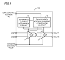
- Fig. 1 is a block diagram showing a voltage controlled variable gain amplifier circuit 100 according to an embodiment of this invention.
- the voltage controlled variable gain amplifier circuit 100 includes a first differential amplifier 1, a second differential amplifier 2, a gain control voltage/current conversion circuit 3 and a reference current generation circuit 4.
- Fig. 2 is a circuit diagram of the first differential circuit 1.
- the second differential amplifier 2 has the same circuit structure as the first differential amplifier 1, and receives differential outputs from the first differential amplifier 1 to operate.
- the voltage controlled variable gain amplifier circuit 100 can be manufactured as a semiconductor integrated circuit chip.
- the voltage controlled variable gain amplifier circuit 100 is structured so that its gain varies linearly and continuously against a gain control voltage. First, basic principles of the voltage controlled variable gain amplifier circuit 100 are explained referring to Fig. 1 and Fig. 2 .
- G 2 gm ⁇ RO.
- the gain control voltage/current conversion circuit 3 basically converts a gain control voltage VC into a gain control current IC that varies linearly against the gain control voltage VC. Therefore, the gain G varies linearly against the gain control voltage VC as shown in Fig. 6 , when the drain currents Id1 and Id2 of the first and second differential transistor 11 and 12 are configured so as to vary linearly against the gain control current IC.
- the structure of the first differential amplifier 1 will be explained referring to Fig. 2 .
- the second differential amplifier 2 has the same structure as the first differential amplifier 1, as described above.
- the first differential amplifier 1 includes the first differential input transistor 11 made of a P-channel type MOS transistor, the second differential input transistor 12 made of a P-channel type MOS transistor, constant current source transistors 13, 14 and 15 made of P-channel type MOS transistors, a first current mirror circuit made of N-channel type MOS transistors 16 and 17, a second current mirror circuit made of N-channel type MOS transistors 18 and 19, a first phase compensation circuit 20 and a second phase compensation circuit 21 each made of a capacitor for phase compensation and a resistor for zero cancellation, a first output resistor 22, a second output resistor 23, a first capacitor C1 and a second capacitor C2.
- first differential amplifier 1 is provided with a current bypass circuit 50 that will be described later referring to Fig. 4 , the structure of the first differential amplifier 1 excluding the current bypass circuit 50 is explained here.
- a power supply voltage VDD is applied to a source of each of the constant current source transistors 13, 14 and 15.
- a drain of the constant current source transistor 13 is connected with a common source of the first and second differential input transistors 11 and 12.
- a bias voltage from the reference current generation circuit 4 is applied to a gate of the constant current source transistor 13 so that a constant drain current 2 ⁇ Id 1 flows as a reference current. While each of the drain currents Id1 and Id2 flows through each of the first and second differential input transistors 11 and 12, respectively, the first and second differential input transistors 11 and 12 are assumed to have a size and electric characteristics identical to each other so that Id1 is equal to Id2.
- the first current mirror circuit is connected to a drain of the first differential input transistor 11, and the second current mirror circuit is connected to a drain of the second differential input transistor 12.
- a common bias voltage is applied to a gate of each of the constant current source transistors 14 and 15.
- Each of differential input voltages VIN and VIP is applied to a gate of each of the first and second differential input transistors 11 and 12, respectively.
- a differential output voltage VOP is outputted from a first output terminal 24 connected to a connecting node between the constant current source transistor 15 and the N-channel type MOS transistor 19, while another differential output voltage VON is outputted from a second output terminal 25 connected to a connecting node between the constant current source transistor 14 and the N-channel type MOS transistor 16.
- the first output resistor 22 and the second output resistor 23 are connected in series between the first output terminal 24 and the second output terminal 25.
- the first capacitor C1 is connected in parallel with the first output resistor 22, while the second capacitor C2 is connected in parallel with the second output resistor 23.
- a connecting node between the first output resistor 22 and the second output resistor 23 is adjusted to a constant common voltage VCOM (central voltage).
- the gain G1 of the first differential amplifier 1 and the total gain G of the voltage controlled variable gain amplifier circuit 100 will be determined hereafter.
- VIN varies by ⁇ VIN
- the drain current Id1 of the first differential input transistor 11 varies by ⁇ Id1 accordingly.
- the gate size ratio means W/L that is a ratio of a channel width W to a channel length L of the first differential input transistor 11. The same applies in the rest of the description.
- the gain G1 is proportional to Id ⁇ 1 .
- the gain control voltage/current conversion circuit 3 converts the gain control voltage VC into the gain control current IC that varies linearly against the gain control voltage VC, as described above.
- the current bypass circuit 50 is structured so that the drain currents Id1 and Id2 of the first and second differential input transistors 11 and 12 vary linearly against the gain control current IC.
- the gain control voltage/current conversion circuit 3 basically performs voltage/current conversion using a resistor 34, and converts the gain control voltage VC into a first gain control current IC1 and a second gain control current IC2 that vary linearly against the gain control voltage VC.
- Each of IC1 and IC2 is supplied to each of the first and second differential amplifiers 1 and 2 through a current mirror circuit, respectively.
- Fig. 3A is a circuit diagram of the gain control voltage/current conversion circuit 3.
- the gain control voltage/current conversion circuit 3 includes a gain voltage control circuit 31, an operational amplifier 32, a control transistor 33 made of a P-channel type MOS transistor, the resistor 34 for voltage/current conversion, a buffer amplifier 35, a phase compensation circuit 36 for preventing oscillation, and first and second mirror transistors 37 and 38 made of P-channel type MOS transistors, and is structured as shown in Fig. 3A .
- the gain voltage control circuit 31 generates an inverted gain control voltage VC2 by inverting the gain control voltage VC with respect to a reference voltage VREF of a DC level.
- the gain voltage control circuit 31 is composed of an operational amplifier 310 having an inverting input terminal (-) to which the gain control voltage VC is applied through an input resistor 311 and a non-inverting input terminal (+) to which the reference voltage VREF is applied and a feedback resistor 312 connected between the inverting input terminal (-) and an output terminal of the operational amplifier 310 as shown in Fig. 3B , for example.
- Each of resistances of the input resistor 311 and the feedback resistor 312 is Rx.
- the inverted gain control voltage VC2 outputted from the gain voltage control circuit 31 is applied to an inverting input terminal (-) of the operational amplifier 32.
- An output voltage of the operational amplifier 32 is applied to a gate of the control transistor 33 while the power supply voltage VDD is applied to its source.
- a drain of the control transistor 33 is connected to one end of the resistor 34 that has a resistance RC2.
- a connecting node between the control transistor 33 and the resistor 34 is connected to a non-inverting input terminal (+) of the operational amplifier 32.
- a minimum reference voltage VREF_MIN is applied to another end of the resistor 34 through the buffer amplifier 35.
- the operational amplifier 32 makes a control current IC0 flow through the control transistor 33 so that a voltage at the one end of the resistor 34 becomes VC2.
- ⁇ VC and ⁇ VC2 are defined by Equations 11 and 12, respectively.
- the gain control voltage ⁇ VC varies in a range between - ⁇ VC0 and ⁇ VC0.
- Equation 16 -1/ RC 2 ⁇ VC varies linearly against ⁇ VC, while ⁇ VC 0/ RC 2 is fixed against ⁇ VC. That is, IC0 varies linearly against ⁇ VC.
- Fig. 5 shows a correlation between IC0 and ⁇ VC.
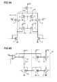
- Fig. 4A is a circuit diagram of the current bypass circuit 50.
- Fig. 4B is a circuit diagram showing connections between the current bypass circuit 50 and the gain control voltage/current conversion circuit 3.
- the current bypass circuit 50 includes a pair of first bypass transistors 51 and 52 made of N-channel type MOS transistors and a pair of second bypass transistors 53 and 54 made of P-channel MOS transistors.
- a drain of the first bypass transistor 51 is connected to a connecting node between the first differential input transistor 11 and the constant current source transistor 13, and its source is grounded.
- a drain of the other first bypass transistor 52 is connected to a connecting node between the second differential input transistor 12 and the constant current source transistor 13, and its source is grounded.
- a drain of the second bypass transistor 53 is connected to a connecting node between the first differential input transistor 11 and a drain of the N-channel type MOS transistor 17 constituting the first current mirror circuit.
- the power supply voltage VDD is applied to a source of the second bypass transistor 53.
- a drain of the other second bypass transistor 54 is connected to a connecting node between the second differential input transistor 12 and a drain of the N-channel type MOS transistor 19 constituting the second current mirror circuit.
- the power supply voltage VDD is applied to a source of the second bypass transistor 54.
- the output of the operational amplifier 32 in the gain control voltage/current conversion circuit 3 is applied to gates of the pair of second bypass transistors 53 and 54, which are connected with each other.
- An N-channel type MOS transistor 55 is connected in series with the first mirror transistor 37. A gate and a drain of the N channel type MOS transistor 55 are connected with each other and its source is grounded. The gate of the N-channel type MOS transistor 55 is connected to gates of the pair of first bypass transistors 51 and 52, which are connected with each other. The N-channel type MOS transistor 55 and the first bypass transistor 51 form a current mirror circuit, while the N-channel type MOS transistor 55 and the other first bypass transistor 52 form another current mirror circuit.
- the gain control current IC1 from the gain control voltage/current conversion circuit 3 flows through each of the pair of first bypass transistors 51 and 52 and each of the pair of second bypass transistors 53 and 54.
- drain current Id1 that is a half of the drain current 2 ⁇ Id 1 of the constant current source transistor 13 flows through the first differential input transistor 11 if the first bypass transistors 51 does not exist, providing the first bypass transistor 51 forms a bypass route through which the gain control current IC1 flows to the ground bypassing the first differential input transistor 11.
- the other first bypass transistor 52 also performs the same function with respect to the second differential input transistor 12.
- the second bypass transistor 53 merges the gain control current IC1, which is the same amount of current as the current bypassed by the first bypass transistor 51, into the drain current of the N-channel type MOS transistor 17 connected to the drain of the first differential input transistor 11. As a result, a constant drain current Id1 flows through the N-channel type MOS transistor 17.
- the other second bypass transistor 54 performs the same function.
- the gain control voltage/current conversion circuit 3 includes the gain voltage control circuit 31 in the embodiment, the gain voltage control circuit 31 may be omitted because it only inverts the polarity of the gain control voltage VC with respect to the reference voltage VREF and has nothing to do with the linearity of the gain G. In that case, the gain G decreases linearly as ⁇ VC increases.
- the gain G of the voltage controlled variable gain amplifier circuit 100 does not have power supply voltage dependence.
- the power supply voltage dependence of the gain G can be improved by composing the reference current generation circuit 4 using a circuit that does not have power supply voltage dependence (for example, a constant gm type reference current generation circuit that is to be described).
- the gain control voltage/current conversion circuit 3 described above has the power supply voltage dependence.
- VDD power supply voltage
- Fig. 7 is a circuit diagram showing such a gain control voltage/current conversion circuit 3A.
- the gain control voltage/current conversion circuit 3A is formed by providing the gain control voltage/current conversion circuit 3 shown in Fig. 3A with a control circuit to suppress the power supply voltage dependence of the gain control current IC1.
- the control circuit includes a resistor 65 (second resistor), a first current generation circuit and a second current generation circuit.
- the resistor 65 has a resistance RC22 and is connected in series with a resistor 34 (first resistor).
- the resistor 65 is connected between a buffer amplifier 35 and the resistor 34.
- a resistance of the resistor 34 is denoted as RC21.
- a current flowing through the resistor 34 through a control transistor 33 is denoted as I2.
- the first current generation circuit includes an N-channel type MOS transistor 66 connected between a connecting node between the resistors 34 and 65 and the ground and a reference current generation circuit 4 that controls the N-channel type MOS transistor 66 so that a current Is not having the power supply voltage dependence flows through the N-channel type MOS transistor 66.
- the reference current generation circuit 4 can be formed of the constant gm type reference current generation circuit that is to be described.
- the reference current generation circuit 4 also controls an N-channel type MOS transistor 67 so that a current IRA not having the power supply voltage dependence flows through the N-channel type MOS transistor 67.
- the current IRA provides the constant current source transistor 13 in each of the first and second differential amplifiers 1 and 2 with the constant drain current 2 ⁇ Id 1 as the reference current through a current mirror circuit (not shown).
- the second current generation circuit includes an operational amplifier 61, control transistors 62 and 63 made of P-channel type MOS transistors and a resistor 64 having a resistance RC1.
- the control transistor 62 and the resistor 64 are connected in series between the power supply voltage VDD and an output terminal of the buffer amplifier 35.
- the control transistor 63 is connected between the power supply voltage VDD and the connecting node between the resistors 34 and 65.
- An output of the operational amplifier 61 is applied to gates of the control transistors 62 and 63.
- the control circuit suppresses the power supply voltage dependence of the current I2 flowing through the resistor 34, because the voltage Vx is varied by that a variation ⁇ I1 in the current I1 due to the variation in the power supply voltage VDD flows through the resistor 65.
- the current I2 can be set equal to each of IC1 and IC2 flowing through each of the first and second mirror transistors 37 and 38, as described above.
- Vx VREF - RC ⁇ 21 ⁇ I ⁇ 2
- I ⁇ 2 RC ⁇ 22 RC ⁇ 21 + RC ⁇ 22 ⁇ 1 RC ⁇ 22 - 1 RC ⁇ 1 ⁇ 0.1 ⁇ VDD + Is
- Fig. 8 shows characteristics of the gain G when the power supply voltage VDD is 3.3V and 5V in the case where the gain control voltage/current conversion circuit 3 before the improvement is used.
- Fig. 9 shows characteristics of the gain G when the power supply voltage VDD is 3.3V and 5V in the case where the improved gain control voltage/current conversion circuit 3A is used. It is understood that the characteristics of the gain G are significantly improved in the case where the improved gain control voltage/current conversion circuit 3A is used.
- the reference current generation circuit 4 provides the constant current source transistor 13 in each of the first and second differential amplifiers 1 and 2 with the drain current 2 ⁇ Id 1 as the reference current, which does not depend on the power supply voltage VDD, as described above. Also, it is used to suppress the power supply voltage dependence of the gain control voltage/current conversion circuit 3A.
- constant gm type reference current generation circuit 4 is used to suppress the variations due to the semiconductor manufacturing processes and the temperature dependence of the gain G of the voltage controlled variable gain amplifier circuit 100.
- Fig. 10 is a circuit diagram of the constant gm type reference current generation circuit 4.
- the constant gm type reference voltage generation circuit 4 includes a resistor 70 having a resistance RB, P-channel type MOS transistors 71, 72, 73 and 74, a bias circuit 75 and N-channel type MOS transistors 76, 77, 78 and 79.
- the P-channel type MOS transistors 71 and 72 are mirror transistors forming a first current mirror circuit.
- the resistor 70 is connected between a source of the P-channel type MOS transistor 71 and the power supply voltage.
- the power supply voltage VDD is applied to a source of the P channel type transistor 72.
- the N-channel type MOS transistors 76 and 77 are mirror transistors forming a second current mirror circuit. Sources of the N-channel type MOS transistors 76 and 77 are grounded. The second current mirror circuit is connected with the first current mirror circuit in series.
- Each of the P-channel type MOS transistors 73 and 74 is cascode-connected to each of the P-channel type MOS transistors 71 and 72, respectively.
- Each of the N-channel type MOS transistors 78 and 79 is cascode-connected to each of the N-channel type MOS transistors 76 and 77, respectively.
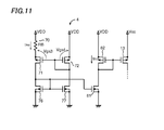
- the P-channel type MOS transistors 73 and 74 and the N-channel type MOS transistors 78 and 79 are omitted as shown in Fig. 11 .
- Cascode-connected N-channel type MOS transistors 80 and 81 make output transistors of the reference current generation circuit 4.
- the bias circuit 75 applies a first bias voltage to gates of the P-channel type MOS transistors 73 and 74.
- the bias circuit 75 also applies a second bias voltage to gates of the N-channel type MOS transistors 78, 79 and 80.
- the N-channel type MOS transistors 76 and 81 form a third current mirror circuit.
- the N-channel type MOS transistor 80 is omitted as shown in Fig. 11 .
- a P-channel type MOS transistor 82 and the N-channel type MOS transistors 80 and 81 are connected in series between the power supply voltage VDD and the ground.
- the constant current source transistor 13 in each of the first and second differential amplifiers 1 and 2 and the P-channel type MOS transistor 82 form a fourth current mirror circuit.
- Vgs3 A voltage between a gate and the source of the P-channel type MOS transistor 71 is denoted as Vgs3
- Vgs4 a voltage between a gate and the source of the P-channel type MOS transistor 72
- I RO reference current
- ⁇ p denotes mobility
- Cox denotes a gate capacitance per unit area of each of the P-channel type MOS transistors 71 and 72
- Vt3 and Vt4 denote threshold voltages of the P-channel MOS transistors 71 and 72, respectively.
- Equation 30 can be modified to Equation 31: 2 ⁇ I RO ⁇ p ⁇ Cox ⁇ S ⁇ 4 ⁇ 1 - 1 K
- I RO 2 ⁇ p ⁇ Cox ⁇ S ⁇ 4 ⁇ 1 RB 2 ⁇ 1 - 1 K 2
- the reference current I RO is inversely proportional to a square of the resistance RB.
- I RO is not affected by the power supply voltage VDD, it is affected by the characteristics ( ⁇ p, Cox) of the P-channel type MOS transistor 71. It is also affected by temperature dependence of the resistance RB.
- the reference current I RO also flows through the P-channel type MOS transistor 82 due to the fourth current mirror circuit (when a mirror ratio ⁇ is 1).
- the gain G1 of the first differential amplifier 1 is determined based on the reference current I RO obtained by the constant gm type reference current generation circuit 4.
- ⁇ is determined by the gate size ratios of the first differential input transistor 11 and the P-channel type MOS transistor 72, while (RO/RB) 2 is determined by a ratio of the resistances. Therefore, the power supply voltage dependence, the variations due to the semiconductor manufacturing processes and the temperature dependence of the total gain G of the voltage controlled variable gain amplifier circuit 100 can be suppressed by adopting the constant gm type reference current generation circuit 4.
- the constant gm type reference current generation circuit 4 is suitable for using in the voltage controlled variable gain amplifier circuit 100 as described above, and may be used in a two-stage amplifier circuit 100A as shown in Fig. 12 and in a single-stage amplifier circuit 100B as shown in Fig. 13 as well. That is, as understood from Equation 34, the variations due to the semiconductor manufacturing processes and the temperature dependence of the gain G1 of the first differential amplifier 1 can be suppressed as well.
- the voltage controlled variable gain amplifier circuit varies its gain linearly and continuously against the gain control voltage, as described above.
- the power supply voltage dependence of the voltage controlled variable gain amplifier circuit is suppressed.
- the variations due to semiconductor manufacturing processes and temperature dependence of the gain of the voltage controlled variable gain amplifier circuit can be also suppressed.
Landscapes
- Engineering & Computer Science (AREA)
- Power Engineering (AREA)
- Control Of Amplification And Gain Control (AREA)
- Amplifiers (AREA)
Applications Claiming Priority (1)
| Application Number | Priority Date | Filing Date | Title |
|---|---|---|---|
| JP2011185729A JP5788739B2 (ja) | 2011-08-29 | 2011-08-29 | 電圧可変利得増幅回路 |
Publications (2)
| Publication Number | Publication Date |
|---|---|
| EP2566049A2 true EP2566049A2 (de) | 2013-03-06 |
| EP2566049A3 EP2566049A3 (de) | 2014-09-10 |
Family
ID=46801325
Family Applications (1)
| Application Number | Title | Priority Date | Filing Date |
|---|---|---|---|
| EP12182170.6A Withdrawn EP2566049A3 (de) | 2011-08-29 | 2012-08-29 | Spannungsgesteuerte Verstärkerschaltung mit variabler Verstärkung |
Country Status (4)
| Country | Link |
|---|---|
| US (1) | US8922279B2 (de) |
| EP (1) | EP2566049A3 (de) |
| JP (1) | JP5788739B2 (de) |
| CN (1) | CN102969994B (de) |
Families Citing this family (4)
| Publication number | Priority date | Publication date | Assignee | Title |
|---|---|---|---|---|
| CN109831171B (zh) * | 2016-05-31 | 2024-06-04 | 深圳市海思半导体有限公司 | 一种可变增益放大器 |
| US10153774B1 (en) * | 2017-01-27 | 2018-12-11 | Cadence Design Systems, Inc. | Transconductor circuit for a fourth order PLL |
| CN116072182B (zh) * | 2023-01-20 | 2025-09-05 | 福建省晋华集成电路有限公司 | 参考电压控制的等化输入数据缓冲电路 |
| WO2026006231A1 (en) * | 2024-06-27 | 2026-01-02 | Micron Technology, Inc. | Semiconductor device having differentia amplifier |
Citations (1)
| Publication number | Priority date | Publication date | Assignee | Title |
|---|---|---|---|---|
| JPH05218767A (ja) | 1992-01-28 | 1993-08-27 | Nec Corp | 可変利得増幅回路 |
Family Cites Families (6)
| Publication number | Priority date | Publication date | Assignee | Title |
|---|---|---|---|---|
| AU691554B2 (en) * | 1994-03-09 | 1998-05-21 | Nec Corporation | Analog multiplier using multitail cell |
| JP2778537B2 (ja) * | 1995-07-14 | 1998-07-23 | 日本電気株式会社 | Agcアンプ |
| FR2818465B1 (fr) * | 2000-12-14 | 2003-03-07 | St Microelectronics Sa | Amplificateur compact a gain ajustable |
| JP4027822B2 (ja) * | 2003-03-11 | 2007-12-26 | 松下電器産業株式会社 | Agc回路 |
| US7973602B2 (en) * | 2009-05-06 | 2011-07-05 | Mindspeed Technologies, Inc. | Variable gain amplifier |
| KR101250439B1 (ko) * | 2009-09-11 | 2013-04-08 | 한국전자통신연구원 | Cmos 가변 이득 증폭기 |
-
2011
- 2011-08-29 JP JP2011185729A patent/JP5788739B2/ja active Active
-
2012
- 2012-08-23 CN CN201210303484.8A patent/CN102969994B/zh active Active
- 2012-08-28 US US13/596,882 patent/US8922279B2/en active Active
- 2012-08-29 EP EP12182170.6A patent/EP2566049A3/de not_active Withdrawn
Patent Citations (1)
| Publication number | Priority date | Publication date | Assignee | Title |
|---|---|---|---|---|
| JPH05218767A (ja) | 1992-01-28 | 1993-08-27 | Nec Corp | 可変利得増幅回路 |
Also Published As
| Publication number | Publication date |
|---|---|
| US20130049865A1 (en) | 2013-02-28 |
| US8922279B2 (en) | 2014-12-30 |
| CN102969994B (zh) | 2017-06-13 |
| EP2566049A3 (de) | 2014-09-10 |
| CN102969994A (zh) | 2013-03-13 |
| JP5788739B2 (ja) | 2015-10-07 |
| JP2013048335A (ja) | 2013-03-07 |
Similar Documents
| Publication | Publication Date | Title |
|---|---|---|
| KR101926003B1 (ko) | 초저 작동 전압 레일 대 레일 연산 증폭기 및 차동 입력 증폭단 회로 및 그 출력단 회로 | |
| US7746168B2 (en) | Bias circuit | |
| JP2009105810A (ja) | 増幅装置及びバイアス回路 | |
| WO2002087072A2 (en) | Bias method and circuit for distortion reduction | |
| JP2010268350A (ja) | 終端抵抗調整回路 | |
| KR20120064617A (ko) | 볼티지 레귤레이터 | |
| US9523995B2 (en) | Reference voltage circuit | |
| EP2566049A2 (de) | Spannungsgesteuerte Verstärkerschaltung mit variabler Verstärkung | |
| US7061309B2 (en) | Transconductance-adjusting circuit | |
| JP6132881B2 (ja) | 電圧可変利得増幅回路及び差動入力電圧の増幅方法 | |
| EP2058944B1 (de) | Transkonduktanzverstärker | |
| US9455676B2 (en) | Semiconductor circuit and amplifier circuit | |
| US7859339B2 (en) | Differential amplification circuit | |
| US11632091B2 (en) | Operational amplifier | |
| US20150263679A1 (en) | Inverting amplifier | |
| CN101859160B (zh) | 一种超低电源电压的带隙基准源 | |
| US8624628B1 (en) | Adjustable level shifter | |
| JP4694942B2 (ja) | 定電流回路 | |
| CN114124003B (zh) | 运算放大器 | |
| US6400185B2 (en) | Fixed transconductance bias apparatus | |
| JP2012104948A (ja) | 増幅回路 | |
| JP2008306562A (ja) | 演算増幅器 | |
| JPH10112614A (ja) | バイアス電流供給方法およびその回路 | |
| JP2005354558A (ja) | 差動増幅回路 | |
| WO2004042782A2 (en) | Apparatus and method for implementing a constant transconductance circuit |
Legal Events
| Date | Code | Title | Description |
|---|---|---|---|
| PUAI | Public reference made under article 153(3) epc to a published international application that has entered the european phase |
Free format text: ORIGINAL CODE: 0009012 |
|
| AK | Designated contracting states |
Kind code of ref document: A2 Designated state(s): AL AT BE BG CH CY CZ DE DK EE ES FI FR GB GR HR HU IE IS IT LI LT LU LV MC MK MT NL NO PL PT RO RS SE SI SK SM TR |
|
| AX | Request for extension of the european patent |
Extension state: BA ME |
|
| PUAL | Search report despatched |
Free format text: ORIGINAL CODE: 0009013 |
|
| AK | Designated contracting states |
Kind code of ref document: A3 Designated state(s): AL AT BE BG CH CY CZ DE DK EE ES FI FR GB GR HR HU IE IS IT LI LT LU LV MC MK MT NL NO PL PT RO RS SE SI SK SM TR |
|
| AX | Request for extension of the european patent |
Extension state: BA ME |
|
| RIC1 | Information provided on ipc code assigned before grant |
Ipc: H03G 1/00 20060101AFI20140801BHEP |
|
| STAA | Information on the status of an ep patent application or granted ep patent |
Free format text: STATUS: THE APPLICATION IS DEEMED TO BE WITHDRAWN |
|
| 18D | Application deemed to be withdrawn |
Effective date: 20150303 |