EP2559057B1 - Improved debonding equipment and methods for debonding temporary bonded wafers - Google Patents
Improved debonding equipment and methods for debonding temporary bonded wafers Download PDFInfo
- Publication number
- EP2559057B1 EP2559057B1 EP11769635.1A EP11769635A EP2559057B1 EP 2559057 B1 EP2559057 B1 EP 2559057B1 EP 11769635 A EP11769635 A EP 11769635A EP 2559057 B1 EP2559057 B1 EP 2559057B1
- Authority
- EP
- European Patent Office
- Prior art keywords
- wafer
- chuck
- flex plate
- edge
- contact
- Prior art date
- Legal status (The legal status is an assumption and is not a legal conclusion. Google has not performed a legal analysis and makes no representation as to the accuracy of the status listed.)
- Active
Links
- 235000012431 wafers Nutrition 0.000 title claims description 383
- 238000000034 method Methods 0.000 title claims description 66
- 230000008569 process Effects 0.000 claims description 41
- 239000010410 layer Substances 0.000 claims description 34
- 239000012790 adhesive layer Substances 0.000 claims description 27
- 230000032798 delamination Effects 0.000 claims description 6
- 229910010293 ceramic material Inorganic materials 0.000 claims description 5
- 230000033001 locomotion Effects 0.000 description 24
- 238000012546 transfer Methods 0.000 description 24
- 239000000853 adhesive Substances 0.000 description 21
- 230000001070 adhesive effect Effects 0.000 description 21
- 239000000758 substrate Substances 0.000 description 20
- 238000000926 separation method Methods 0.000 description 12
- 238000010586 diagram Methods 0.000 description 10
- 238000010438 heat treatment Methods 0.000 description 10
- 239000012528 membrane Substances 0.000 description 8
- 239000007789 gas Substances 0.000 description 7
- 230000000712 assembly Effects 0.000 description 6
- 238000000429 assembly Methods 0.000 description 6
- 239000000919 ceramic Substances 0.000 description 6
- 239000011521 glass Substances 0.000 description 5
- 230000015572 biosynthetic process Effects 0.000 description 4
- 239000000463 material Substances 0.000 description 4
- 239000011253 protective coating Substances 0.000 description 4
- 238000007789 sealing Methods 0.000 description 4
- XUIMIQQOPSSXEZ-UHFFFAOYSA-N Silicon Chemical compound [Si] XUIMIQQOPSSXEZ-UHFFFAOYSA-N 0.000 description 3
- 239000002313 adhesive film Substances 0.000 description 3
- 239000011248 coating agent Substances 0.000 description 3
- 238000000576 coating method Methods 0.000 description 3
- 239000012636 effector Substances 0.000 description 3
- 230000007246 mechanism Effects 0.000 description 3
- 239000002184 metal Substances 0.000 description 3
- 238000000623 plasma-assisted chemical vapour deposition Methods 0.000 description 3
- 238000010926 purge Methods 0.000 description 3
- 239000004065 semiconductor Substances 0.000 description 3
- 229910052710 silicon Inorganic materials 0.000 description 3
- 239000010703 silicon Substances 0.000 description 3
- 125000006850 spacer group Chemical group 0.000 description 3
- XLYOFNOQVPJJNP-UHFFFAOYSA-N water Substances O XLYOFNOQVPJJNP-UHFFFAOYSA-N 0.000 description 3
- 241000743339 Agrostis Species 0.000 description 2
- QGZKDVFQNNGYKY-UHFFFAOYSA-N Ammonia Chemical compound N QGZKDVFQNNGYKY-UHFFFAOYSA-N 0.000 description 2
- IJGRMHOSHXDMSA-UHFFFAOYSA-N Atomic nitrogen Chemical compound N#N IJGRMHOSHXDMSA-UHFFFAOYSA-N 0.000 description 2
- 229910001218 Gallium arsenide Inorganic materials 0.000 description 2
- 239000003082 abrasive agent Substances 0.000 description 2
- 230000008901 benefit Effects 0.000 description 2
- 238000013461 design Methods 0.000 description 2
- 238000005286 illumination Methods 0.000 description 2
- 238000009413 insulation Methods 0.000 description 2
- 238000002955 isolation Methods 0.000 description 2
- 238000004519 manufacturing process Methods 0.000 description 2
- 239000002243 precursor Substances 0.000 description 2
- 230000036316 preload Effects 0.000 description 2
- 238000012545 processing Methods 0.000 description 2
- 230000001681 protective effect Effects 0.000 description 2
- 229920002379 silicone rubber Polymers 0.000 description 2
- 239000002002 slurry Substances 0.000 description 2
- 230000003068 static effect Effects 0.000 description 2
- 239000000126 substance Substances 0.000 description 2
- 230000001360 synchronised effect Effects 0.000 description 2
- 238000013519 translation Methods 0.000 description 2
- KRHYYFGTRYWZRS-UHFFFAOYSA-M Fluoride anion Chemical compound [F-] KRHYYFGTRYWZRS-UHFFFAOYSA-M 0.000 description 1
- 208000013201 Stress fracture Diseases 0.000 description 1
- 229920004482 WACKER® Polymers 0.000 description 1
- 239000002390 adhesive tape Substances 0.000 description 1
- 229910021529 ammonia Inorganic materials 0.000 description 1
- 150000001875 compounds Chemical class 0.000 description 1
- 238000001816 cooling Methods 0.000 description 1
- 238000005336 cracking Methods 0.000 description 1
- 238000004132 cross linking Methods 0.000 description 1
- 239000010432 diamond Substances 0.000 description 1
- 229910003460 diamond Inorganic materials 0.000 description 1
- 238000006073 displacement reaction Methods 0.000 description 1
- 229920001971 elastomer Polymers 0.000 description 1
- 239000000806 elastomer Substances 0.000 description 1
- 239000010438 granite Substances 0.000 description 1
- 238000000227 grinding Methods 0.000 description 1
- 239000007788 liquid Substances 0.000 description 1
- 235000015250 liver sausages Nutrition 0.000 description 1
- 238000012986 modification Methods 0.000 description 1
- 230000004048 modification Effects 0.000 description 1
- 229910052757 nitrogen Inorganic materials 0.000 description 1
- 238000005498 polishing Methods 0.000 description 1
- 239000000843 powder Substances 0.000 description 1
- 238000003825 pressing Methods 0.000 description 1
- 239000011241 protective layer Substances 0.000 description 1
- 239000010453 quartz Substances 0.000 description 1
- 230000005855 radiation Effects 0.000 description 1
- 230000009467 reduction Effects 0.000 description 1
- 229910052594 sapphire Inorganic materials 0.000 description 1
- 239000010980 sapphire Substances 0.000 description 1
- 230000035939 shock Effects 0.000 description 1
- HBMJWWWQQXIZIP-UHFFFAOYSA-N silicon carbide Chemical compound [Si+]#[C-] HBMJWWWQQXIZIP-UHFFFAOYSA-N 0.000 description 1
- 229910010271 silicon carbide Inorganic materials 0.000 description 1
- VYPSYNLAJGMNEJ-UHFFFAOYSA-N silicon dioxide Inorganic materials O=[Si]=O VYPSYNLAJGMNEJ-UHFFFAOYSA-N 0.000 description 1
- 238000005549 size reduction Methods 0.000 description 1
- 238000004528 spin coating Methods 0.000 description 1
- 238000012876 topography Methods 0.000 description 1
Images
Classifications
-
- B—PERFORMING OPERATIONS; TRANSPORTING
- B32—LAYERED PRODUCTS
- B32B—LAYERED PRODUCTS, i.e. PRODUCTS BUILT-UP OF STRATA OF FLAT OR NON-FLAT, e.g. CELLULAR OR HONEYCOMB, FORM
- B32B43/00—Operations specially adapted for layered products and not otherwise provided for, e.g. repairing; Apparatus therefor
- B32B43/006—Delaminating
-
- H—ELECTRICITY
- H01—ELECTRIC ELEMENTS
- H01L—SEMICONDUCTOR DEVICES NOT COVERED BY CLASS H10
- H01L21/00—Processes or apparatus adapted for the manufacture or treatment of semiconductor or solid state devices or of parts thereof
- H01L21/67—Apparatus specially adapted for handling semiconductor or electric solid state devices during manufacture or treatment thereof; Apparatus specially adapted for handling wafers during manufacture or treatment of semiconductor or electric solid state devices or components ; Apparatus not specifically provided for elsewhere
- H01L21/67005—Apparatus not specifically provided for elsewhere
- H01L21/67011—Apparatus for manufacture or treatment
- H01L21/67092—Apparatus for mechanical treatment
-
- H—ELECTRICITY
- H01—ELECTRIC ELEMENTS
- H01L—SEMICONDUCTOR DEVICES NOT COVERED BY CLASS H10
- H01L21/00—Processes or apparatus adapted for the manufacture or treatment of semiconductor or solid state devices or of parts thereof
- H01L21/67—Apparatus specially adapted for handling semiconductor or electric solid state devices during manufacture or treatment thereof; Apparatus specially adapted for handling wafers during manufacture or treatment of semiconductor or electric solid state devices or components ; Apparatus not specifically provided for elsewhere
- H01L21/67005—Apparatus not specifically provided for elsewhere
- H01L21/67011—Apparatus for manufacture or treatment
- H01L21/67098—Apparatus for thermal treatment
- H01L21/67103—Apparatus for thermal treatment mainly by conduction
-
- H—ELECTRICITY
- H01—ELECTRIC ELEMENTS
- H01L—SEMICONDUCTOR DEVICES NOT COVERED BY CLASS H10
- H01L21/00—Processes or apparatus adapted for the manufacture or treatment of semiconductor or solid state devices or of parts thereof
- H01L21/67—Apparatus specially adapted for handling semiconductor or electric solid state devices during manufacture or treatment thereof; Apparatus specially adapted for handling wafers during manufacture or treatment of semiconductor or electric solid state devices or components ; Apparatus not specifically provided for elsewhere
- H01L21/67005—Apparatus not specifically provided for elsewhere
- H01L21/67011—Apparatus for manufacture or treatment
- H01L21/67132—Apparatus for placing on an insulating substrate, e.g. tape
-
- H—ELECTRICITY
- H01—ELECTRIC ELEMENTS
- H01L—SEMICONDUCTOR DEVICES NOT COVERED BY CLASS H10
- H01L21/00—Processes or apparatus adapted for the manufacture or treatment of semiconductor or solid state devices or of parts thereof
- H01L21/67—Apparatus specially adapted for handling semiconductor or electric solid state devices during manufacture or treatment thereof; Apparatus specially adapted for handling wafers during manufacture or treatment of semiconductor or electric solid state devices or components ; Apparatus not specifically provided for elsewhere
- H01L21/68—Apparatus specially adapted for handling semiconductor or electric solid state devices during manufacture or treatment thereof; Apparatus specially adapted for handling wafers during manufacture or treatment of semiconductor or electric solid state devices or components ; Apparatus not specifically provided for elsewhere for positioning, orientation or alignment
-
- H—ELECTRICITY
- H01—ELECTRIC ELEMENTS
- H01L—SEMICONDUCTOR DEVICES NOT COVERED BY CLASS H10
- H01L21/00—Processes or apparatus adapted for the manufacture or treatment of semiconductor or solid state devices or of parts thereof
- H01L21/67—Apparatus specially adapted for handling semiconductor or electric solid state devices during manufacture or treatment thereof; Apparatus specially adapted for handling wafers during manufacture or treatment of semiconductor or electric solid state devices or components ; Apparatus not specifically provided for elsewhere
- H01L21/683—Apparatus specially adapted for handling semiconductor or electric solid state devices during manufacture or treatment thereof; Apparatus specially adapted for handling wafers during manufacture or treatment of semiconductor or electric solid state devices or components ; Apparatus not specifically provided for elsewhere for supporting or gripping
- H01L21/6835—Apparatus specially adapted for handling semiconductor or electric solid state devices during manufacture or treatment thereof; Apparatus specially adapted for handling wafers during manufacture or treatment of semiconductor or electric solid state devices or components ; Apparatus not specifically provided for elsewhere for supporting or gripping using temporarily an auxiliary support
-
- H—ELECTRICITY
- H01—ELECTRIC ELEMENTS
- H01L—SEMICONDUCTOR DEVICES NOT COVERED BY CLASS H10
- H01L21/00—Processes or apparatus adapted for the manufacture or treatment of semiconductor or solid state devices or of parts thereof
- H01L21/67—Apparatus specially adapted for handling semiconductor or electric solid state devices during manufacture or treatment thereof; Apparatus specially adapted for handling wafers during manufacture or treatment of semiconductor or electric solid state devices or components ; Apparatus not specifically provided for elsewhere
- H01L21/683—Apparatus specially adapted for handling semiconductor or electric solid state devices during manufacture or treatment thereof; Apparatus specially adapted for handling wafers during manufacture or treatment of semiconductor or electric solid state devices or components ; Apparatus not specifically provided for elsewhere for supporting or gripping
- H01L21/6838—Apparatus specially adapted for handling semiconductor or electric solid state devices during manufacture or treatment thereof; Apparatus specially adapted for handling wafers during manufacture or treatment of semiconductor or electric solid state devices or components ; Apparatus not specifically provided for elsewhere for supporting or gripping with gripping and holding devices using a vacuum; Bernoulli devices
-
- B—PERFORMING OPERATIONS; TRANSPORTING
- B32—LAYERED PRODUCTS
- B32B—LAYERED PRODUCTS, i.e. PRODUCTS BUILT-UP OF STRATA OF FLAT OR NON-FLAT, e.g. CELLULAR OR HONEYCOMB, FORM
- B32B2309/00—Parameters for the laminating or treatment process; Apparatus details
- B32B2309/08—Dimensions, e.g. volume
- B32B2309/10—Dimensions, e.g. volume linear, e.g. length, distance, width
- B32B2309/105—Thickness
-
- B—PERFORMING OPERATIONS; TRANSPORTING
- B32—LAYERED PRODUCTS
- B32B—LAYERED PRODUCTS, i.e. PRODUCTS BUILT-UP OF STRATA OF FLAT OR NON-FLAT, e.g. CELLULAR OR HONEYCOMB, FORM
- B32B2457/00—Electrical equipment
- B32B2457/14—Semiconductor wafers
-
- B—PERFORMING OPERATIONS; TRANSPORTING
- B32—LAYERED PRODUCTS
- B32B—LAYERED PRODUCTS, i.e. PRODUCTS BUILT-UP OF STRATA OF FLAT OR NON-FLAT, e.g. CELLULAR OR HONEYCOMB, FORM
- B32B38/00—Ancillary operations in connection with laminating processes
- B32B38/18—Handling of layers or the laminate
- B32B38/1858—Handling of layers or the laminate using vacuum
-
- H—ELECTRICITY
- H01—ELECTRIC ELEMENTS
- H01L—SEMICONDUCTOR DEVICES NOT COVERED BY CLASS H10
- H01L2221/00—Processes or apparatus adapted for the manufacture or treatment of semiconductor or solid state devices or of parts thereof covered by H01L21/00
- H01L2221/67—Apparatus for handling semiconductor or electric solid state devices during manufacture or treatment thereof; Apparatus for handling wafers during manufacture or treatment of semiconductor or electric solid state devices or components; Apparatus not specifically provided for elsewhere
- H01L2221/683—Apparatus for handling semiconductor or electric solid state devices during manufacture or treatment thereof; Apparatus for handling wafers during manufacture or treatment of semiconductor or electric solid state devices or components; Apparatus not specifically provided for elsewhere for supporting or gripping
- H01L2221/68304—Apparatus for handling semiconductor or electric solid state devices during manufacture or treatment thereof; Apparatus for handling wafers during manufacture or treatment of semiconductor or electric solid state devices or components; Apparatus not specifically provided for elsewhere for supporting or gripping using temporarily an auxiliary support
- H01L2221/68318—Auxiliary support including means facilitating the separation of a device or wafer from the auxiliary support
-
- H—ELECTRICITY
- H01—ELECTRIC ELEMENTS
- H01L—SEMICONDUCTOR DEVICES NOT COVERED BY CLASS H10
- H01L2221/00—Processes or apparatus adapted for the manufacture or treatment of semiconductor or solid state devices or of parts thereof covered by H01L21/00
- H01L2221/67—Apparatus for handling semiconductor or electric solid state devices during manufacture or treatment thereof; Apparatus for handling wafers during manufacture or treatment of semiconductor or electric solid state devices or components; Apparatus not specifically provided for elsewhere
- H01L2221/683—Apparatus for handling semiconductor or electric solid state devices during manufacture or treatment thereof; Apparatus for handling wafers during manufacture or treatment of semiconductor or electric solid state devices or components; Apparatus not specifically provided for elsewhere for supporting or gripping
- H01L2221/68304—Apparatus for handling semiconductor or electric solid state devices during manufacture or treatment thereof; Apparatus for handling wafers during manufacture or treatment of semiconductor or electric solid state devices or components; Apparatus not specifically provided for elsewhere for supporting or gripping using temporarily an auxiliary support
- H01L2221/68327—Apparatus for handling semiconductor or electric solid state devices during manufacture or treatment thereof; Apparatus for handling wafers during manufacture or treatment of semiconductor or electric solid state devices or components; Apparatus not specifically provided for elsewhere for supporting or gripping using temporarily an auxiliary support used during dicing or grinding
-
- H—ELECTRICITY
- H01—ELECTRIC ELEMENTS
- H01L—SEMICONDUCTOR DEVICES NOT COVERED BY CLASS H10
- H01L2221/00—Processes or apparatus adapted for the manufacture or treatment of semiconductor or solid state devices or of parts thereof covered by H01L21/00
- H01L2221/67—Apparatus for handling semiconductor or electric solid state devices during manufacture or treatment thereof; Apparatus for handling wafers during manufacture or treatment of semiconductor or electric solid state devices or components; Apparatus not specifically provided for elsewhere
- H01L2221/683—Apparatus for handling semiconductor or electric solid state devices during manufacture or treatment thereof; Apparatus for handling wafers during manufacture or treatment of semiconductor or electric solid state devices or components; Apparatus not specifically provided for elsewhere for supporting or gripping
- H01L2221/68304—Apparatus for handling semiconductor or electric solid state devices during manufacture or treatment thereof; Apparatus for handling wafers during manufacture or treatment of semiconductor or electric solid state devices or components; Apparatus not specifically provided for elsewhere for supporting or gripping using temporarily an auxiliary support
- H01L2221/68381—Details of chemical or physical process used for separating the auxiliary support from a device or wafer
-
- Y—GENERAL TAGGING OF NEW TECHNOLOGICAL DEVELOPMENTS; GENERAL TAGGING OF CROSS-SECTIONAL TECHNOLOGIES SPANNING OVER SEVERAL SECTIONS OF THE IPC; TECHNICAL SUBJECTS COVERED BY FORMER USPC CROSS-REFERENCE ART COLLECTIONS [XRACs] AND DIGESTS
- Y10—TECHNICAL SUBJECTS COVERED BY FORMER USPC
- Y10T—TECHNICAL SUBJECTS COVERED BY FORMER US CLASSIFICATION
- Y10T156/00—Adhesive bonding and miscellaneous chemical manufacture
- Y10T156/11—Methods of delaminating, per se; i.e., separating at bonding face
- Y10T156/1126—Using direct fluid current against work during delaminating
- Y10T156/1132—Using vacuum directly against work during delaminating
-
- Y—GENERAL TAGGING OF NEW TECHNOLOGICAL DEVELOPMENTS; GENERAL TAGGING OF CROSS-SECTIONAL TECHNOLOGIES SPANNING OVER SEVERAL SECTIONS OF THE IPC; TECHNICAL SUBJECTS COVERED BY FORMER USPC CROSS-REFERENCE ART COLLECTIONS [XRACs] AND DIGESTS
- Y10—TECHNICAL SUBJECTS COVERED BY FORMER USPC
- Y10T—TECHNICAL SUBJECTS COVERED BY FORMER US CLASSIFICATION
- Y10T156/00—Adhesive bonding and miscellaneous chemical manufacture
- Y10T156/11—Methods of delaminating, per se; i.e., separating at bonding face
- Y10T156/1168—Gripping and pulling work apart during delaminating
- Y10T156/1174—Using roller for delamination [e.g., roller pairs operating at differing speeds or directions, etc.]
-
- Y—GENERAL TAGGING OF NEW TECHNOLOGICAL DEVELOPMENTS; GENERAL TAGGING OF CROSS-SECTIONAL TECHNOLOGIES SPANNING OVER SEVERAL SECTIONS OF THE IPC; TECHNICAL SUBJECTS COVERED BY FORMER USPC CROSS-REFERENCE ART COLLECTIONS [XRACs] AND DIGESTS
- Y10—TECHNICAL SUBJECTS COVERED BY FORMER USPC
- Y10T—TECHNICAL SUBJECTS COVERED BY FORMER US CLASSIFICATION
- Y10T156/00—Adhesive bonding and miscellaneous chemical manufacture
- Y10T156/11—Methods of delaminating, per se; i.e., separating at bonding face
- Y10T156/1168—Gripping and pulling work apart during delaminating
- Y10T156/1179—Gripping and pulling work apart during delaminating with poking during delaminating [e.g., jabbing, etc.]
- Y10T156/1184—Piercing layer during delaminating [e.g., cutting, etc.]
-
- Y—GENERAL TAGGING OF NEW TECHNOLOGICAL DEVELOPMENTS; GENERAL TAGGING OF CROSS-SECTIONAL TECHNOLOGIES SPANNING OVER SEVERAL SECTIONS OF THE IPC; TECHNICAL SUBJECTS COVERED BY FORMER USPC CROSS-REFERENCE ART COLLECTIONS [XRACs] AND DIGESTS
- Y10—TECHNICAL SUBJECTS COVERED BY FORMER USPC
- Y10T—TECHNICAL SUBJECTS COVERED BY FORMER US CLASSIFICATION
- Y10T156/00—Adhesive bonding and miscellaneous chemical manufacture
- Y10T156/11—Methods of delaminating, per se; i.e., separating at bonding face
- Y10T156/1168—Gripping and pulling work apart during delaminating
- Y10T156/1189—Gripping and pulling work apart during delaminating with shearing during delaminating
-
- Y—GENERAL TAGGING OF NEW TECHNOLOGICAL DEVELOPMENTS; GENERAL TAGGING OF CROSS-SECTIONAL TECHNOLOGIES SPANNING OVER SEVERAL SECTIONS OF THE IPC; TECHNICAL SUBJECTS COVERED BY FORMER USPC CROSS-REFERENCE ART COLLECTIONS [XRACs] AND DIGESTS
- Y10—TECHNICAL SUBJECTS COVERED BY FORMER USPC
- Y10T—TECHNICAL SUBJECTS COVERED BY FORMER US CLASSIFICATION
- Y10T156/00—Adhesive bonding and miscellaneous chemical manufacture
- Y10T156/19—Delaminating means
- Y10T156/1928—Differential fluid pressure delaminating means
- Y10T156/1933—Spraying delaminating means [e.g., atomizer, etc.
- Y10T156/1939—Air blasting delaminating means]
-
- Y—GENERAL TAGGING OF NEW TECHNOLOGICAL DEVELOPMENTS; GENERAL TAGGING OF CROSS-SECTIONAL TECHNOLOGIES SPANNING OVER SEVERAL SECTIONS OF THE IPC; TECHNICAL SUBJECTS COVERED BY FORMER USPC CROSS-REFERENCE ART COLLECTIONS [XRACs] AND DIGESTS
- Y10—TECHNICAL SUBJECTS COVERED BY FORMER USPC
- Y10T—TECHNICAL SUBJECTS COVERED BY FORMER US CLASSIFICATION
- Y10T156/00—Adhesive bonding and miscellaneous chemical manufacture
- Y10T156/19—Delaminating means
- Y10T156/1928—Differential fluid pressure delaminating means
- Y10T156/1944—Vacuum delaminating means [e.g., vacuum chamber, etc.]
-
- Y—GENERAL TAGGING OF NEW TECHNOLOGICAL DEVELOPMENTS; GENERAL TAGGING OF CROSS-SECTIONAL TECHNOLOGIES SPANNING OVER SEVERAL SECTIONS OF THE IPC; TECHNICAL SUBJECTS COVERED BY FORMER USPC CROSS-REFERENCE ART COLLECTIONS [XRACs] AND DIGESTS
- Y10—TECHNICAL SUBJECTS COVERED BY FORMER USPC
- Y10T—TECHNICAL SUBJECTS COVERED BY FORMER US CLASSIFICATION
- Y10T156/00—Adhesive bonding and miscellaneous chemical manufacture
- Y10T156/19—Delaminating means
- Y10T156/195—Delaminating roller means
- Y10T156/1956—Roller pair delaminating means
-
- Y—GENERAL TAGGING OF NEW TECHNOLOGICAL DEVELOPMENTS; GENERAL TAGGING OF CROSS-SECTIONAL TECHNOLOGIES SPANNING OVER SEVERAL SECTIONS OF THE IPC; TECHNICAL SUBJECTS COVERED BY FORMER USPC CROSS-REFERENCE ART COLLECTIONS [XRACs] AND DIGESTS
- Y10—TECHNICAL SUBJECTS COVERED BY FORMER USPC
- Y10T—TECHNICAL SUBJECTS COVERED BY FORMER US CLASSIFICATION
- Y10T156/00—Adhesive bonding and miscellaneous chemical manufacture
- Y10T156/19—Delaminating means
- Y10T156/1961—Severing delaminating means [e.g., chisel, etc.]
- Y10T156/1967—Cutting delaminating means
-
- Y—GENERAL TAGGING OF NEW TECHNOLOGICAL DEVELOPMENTS; GENERAL TAGGING OF CROSS-SECTIONAL TECHNOLOGIES SPANNING OVER SEVERAL SECTIONS OF THE IPC; TECHNICAL SUBJECTS COVERED BY FORMER USPC CROSS-REFERENCE ART COLLECTIONS [XRACs] AND DIGESTS
- Y10—TECHNICAL SUBJECTS COVERED BY FORMER USPC
- Y10T—TECHNICAL SUBJECTS COVERED BY FORMER US CLASSIFICATION
- Y10T156/00—Adhesive bonding and miscellaneous chemical manufacture
- Y10T156/19—Delaminating means
- Y10T156/1978—Delaminating bending means
Definitions
- the present invention relates to improved debonding equipment and methods for debonding temporary bonded wafers, and more particularly to industrial-scale debonding equipment based on thermal slide or mechanical separation.
- wafer thinning steps In some applications the wafers are thinned down to a thickness of less than 100 micrometers for the fabrication of integrated circuit (IC) devices. Thin wafers have the advantages of improved heat removal and better electrical operation of the fabricated IC devices. In one example, GaAs wafers are thinned down to 25 micrometers to fabricate power CMOS devices with improved heat removal. Wafer thinning also contributes to a reduction of the device capacitance and to an increase of its impedance, both of which result in an overall size reduction of the fabricated device. In other applications, wafer thinning is used for 3D-Integration bonding and for fabricating through wafer vias.
- IC integrated circuit
- Wafer thinning is usually performed via back-grinding and/or chemical mechanical polishing (CMP).
- CMP involves bringing the wafer surface into contact with a hard and flat rotating horizontal platter in the presence of a liquid slurry.
- the slurry usually contains abrasive powders, such as diamond or silicon carbide, along with chemical etchants such as ammonia, fluoride, or combinations thereof.
- the abrasives cause substrate thinning, while the etchants polish the substrate surface at the submicron level.
- the wafer is maintained in contact with the abrasives until a certain amount of substrate has been removed in order to achieve a targeted thickness.
- the wafer For wafer thicknesses of over 200 micrometers, the wafer is usually held in place with a fixture that utilizes a vacuum chuck or some other means of mechanical attachment.
- a fixture that utilizes a vacuum chuck or some other means of mechanical attachment.
- An alternative to mechanical holding of the wafers during thinning involves attaching a first surface of the device wafer (i.e., wafer processed into a device) onto a carrier wafer and thinning down the exposed opposite device wafer surface.
- the bond between the carrier wafer and the device wafer is temporary and is removed upon completion of the thinning and any other processing steps.
- JP 2008 306120 A discloses a debonder apparatus for separating a wafer from a glass plate with a chuck assembly comprising a chuck and a wafer holder configured to hold the wafer, and a flex plate assembly comprising a flex plate and a glass plate holder configured to hold the glass plate.
- the flex plate is configured to be placed above the top surface of the chuck.
- the debonder apparatus further discloses means for pushing and lifting up a first edge of the flex plate and a resistance device for applying a downward force upon the flex plate to separate the wafer and the glass plate.
- WO 2010/026910 A1 shows an apparatus for removing an adhesive sheet from a wafer using a peeling tape and two rollers that are moved along the top surface of the wafer to be peeled in order to remove the adhesive sheet.
- JP 2008 066522 A discloses an apparatus for applying a double-sided adhesive tape to a wafer using rollers.
- US 2008/0017311 A1 shows an apparatus for removing a protective sheet from a wafer using a peeling tape.
- the peeling tape and with that the protective sheet are pulled by a roboter arm while a wedge-shaped resistance element is used to apply a downward force onto the wafer.
- the present invention relates to improved debonding equipment and methods for debonding temporary bonded wafers, and more particularly to industrial-scale debonding equipment based mechanical separation.
- the invention features a debonder apparatus for debonding a temporary bonded wafer pair including a chuck assembly, a flex plate assembly, a contact roller and a resistance roller.
- the chuck assembly includes a chuck and a first wafer holder configured to hold a first wafer of the temporary bonded wafer pair in contact with a top surface of the chuck.
- the flex plate assembly includes a flex plate and a second wafer holder configured to hold a second wafer of the temporary bonded wafer pair in contact with a first surface of the flex plate.
- the flex plate is configured to be placed above the top surface of the chuck.
- the contact roller is arranged adjacent to a first edge of the chuck and includes means for pushing and lifting up a first edge of the flex plate.
- the resistance roller includes means for traversing horizontally over the flex plate and means for applying a downward force upon the flex plate. The contact roller pushes and lifts up the first edge of the flex plate while the resistance roller simultaneously applies the downward force upon the flex plate and traverses horizontally away from the first edge of the flex plate and thereby the temporary bonded wafer pair delaminates along a release layer and the first and second wafers are separated from each other.
- the debonder apparatus further includes means for maintaining the angle between the separated wafers constant during the delamination process.
- the means for maintaining the angle between the separated wafers constant during the delamination process comprise means for initially balancing the resistance roller downward force by the contact roller push of the first edge of the flex plate and means for subsequently reducing the resistance roller downward force while the resistance roller is horizontally traversed.
- the flex plate comprises a second edge connected to a hinge, and the second edge is diametrically opposite to the first edge, and the flex plate is configured to swing around the hinge and to be placed above the top surface of the chuck.
- the debonder apparatus further includes a debond drive motor configured to move the contact roller vertical to the plane of the chuck top surface.
- the wafer pair comprises the first wafer stacked upon and being temporarily bonded to the second wafer via an adhesive layer and the release layer.
- the wafer pair is placed upon the chuck so that the ubonded surface of the first wafer is in contact with the chuck top surface.
- the flex plate swings around the hinge and is placed above the bottom chuck so that its first surface is in contact with the unbonded surface of the second wafer.
- the contact roller is driven upward until it contacts and pushes the second edge of the flex plate up while the second wafer is held by the flex plate and the first wafer is held by the chuck via the second and first wafer holders, respectively.
- the debonder apparatus further includes a hinge motor and the hinge is driven by the hinge motor.
- the first and second holders comprise vacuum pulling through the chuck and the flex plate, respectively.
- the wafer pair further comprises a tape frame and the first wafer is held by the chuck by holding the tape frame via vacuum pulled through the chuck.
- the debonder apparatus further includes a support plate supporting the chuck assembly, the flex plate assembly and the hinge.
- the debonder apparatus further includes a base plate supporting the support plate, the contact roller, the hinge motor and the debond drive motor.
- the chuck assembly further comprises a lift pin assembly designed to raise and lower wafers placed on the top surface of the chuck.
- the flex plate further comprises two independently controlled concentric vacuum zones configured to hold wafers having a diameter of 200 or 300 millimeters, respectively.
- the concentric vacuum zones are sealed via one of an O-ring or suction cups.
- the chuck comprises a vacuum chuck made of porous ceramic materials.
- the debonder apparatus further includes an anti-backlash gear drive configured to prevent accidental back swing of the flex pate.
- the invention features a method for debonding a temporary bonded wafer pair including the following steps: First, providing a debonder apparatus comprising a chuck assembly, a flex plate assembly, a contact roller and a resistance roller.
- the chuck assembly comprises a chuck and a first wafer holder configured to hold wafers in contact with a top surface of the chuck.
- the flex plate assembly comprises a flex plate and a second wafer holder configured to hold wafers in contact with a first surface of the flex plate.
- the contact roller is arranged adjacent to a first edge of the chuck and comprises means for pushing and lifting up a first edge of the flex plate.
- the resistance roller comprises means for traversing horizontally over the flex plate and means for applying a downward force upon the flex plate.
- providing a temporary bonded wafer pair comprising a first wafer stacked upon and being temporary bonded to a second wafer via an adhesive layer and a release layer.
- placing the wafer pair upon the chuck so that the ubonded surface of the first wafer is in contact with the chuck top surface.
- the method further includes maintaining the angle between the separated wafers constant during the delamination process by initially balancing the resistance roller downward force by the contact roller push of the first edge of the flex plate and subsequently reducing the resistance roller downward force while the resistance roller is horizontally traversed.
- an improved apparatus for temporary wafer bonding 100 includes a temporary bonder cluster 110 and a debonder cluster 120.
- the temporary bonder cluster 110 includes temporary bonder module A, module B, module C, and module D, 210, 310, 410 and 510 respectively.
- Debonder cluster 120 includes a thermal slide debonder A 150, a mechanical debonder B 250 and a radiation /mechanical debonder C 350.
- Bonder cluster 110 facilitates the temporary bonding processes A, B, C, and D, 60a, 70a, 80a and 90a, shown in FIG. 1A , FIG. 2A , FIG. 3A , and FIG. 4 , respectively, among others.
- Debonder cluster 120 facilitates the debonding processes A, B and C, 60b, 70b, 80b, shown in FIG. 1A , FIG. 2A and FIG. 3A , respectively.
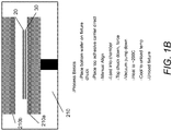
- temporary bond process A 60a includes the following steps. First, device wafer 20 is coated with a protective coating 21 (62), the coating is then baked and chilled (63) and then the wafer is flipped (64). A carrier wafer 30 is coated with an adhesive layer 31 (65) and then the coating is baked and chilled (66). In other embodiments, a dry adhesive film is laminated onto the carrier wafer, instead of coating an adhesive layer. Next, the flipped device wafer 20 is aligned with the carrier wafer 30 so that the surface of the device wafer with the protective coating 20a is opposite to the surface of the carrier wafer with the adhesive layer 30a (67) and then the two wafers are bonded (68) in temporary bonder module A, shown in FIG. 1B .
- the bond is a temporary bond between the protective layer 21 and the adhesive layer 31.
- no protective coating is applied onto the device wafer surface and the device wafer surface 20a is directly bonded with the adhesive layer 31.
- Examples of device wafers include GaAs wafers, silicon wafers, or any other semiconductor wafer that needs to be thinned down to less than 100 micrometers. These thin wafers are used in military and telecommunication applications for the fabrication of power amplifiers or other power devices where good heat removal and small power factor are desirable.
- the carrier wafer is usually made of a noncontaminating material that is thermally matched with the device wafer, i.e., has the same coefficient of thermal expansion (CTE).
- carrier wafer materials include silicon, glass, sapphire, quartz or other semiconductor materials.
- the diameter of the carrier wafer is usually the same as or slightly larger than the diameter of the device wafer, in order to support the device wafer edge and prevent cracking or chipping of the device wafer edge.
- the carrier wafer thickness is about 1000 micrometers and the total thickness variation (TTV) is 2-3 micrometers.
- Carrier wafers are recycled and reused after they are debonded from the device wafer.
- adhesive layer 31 is an organic adhesive WaferBONDTM HT-10.10, manufactured by Brewer Science , Missouri, USA. Adhesive 31 is applied via a spin-on process and has a thickness in the range of 9 to 25 micrometers.
- the spin speed is in the rage of 1000 to 2500 rpm and the spin time is between 3-60 second.
- the adhesive layer is baked for 2 min at a temperature between 100 °C to 150 °C and then cured for 1-3 minutes at a temperature between 160 °C to 220 °C.
- WaferBONDTM HT-10.10 layer is optically transparent and is stable up to 220 °C.
- Appendix A depicts the specification for WaferBONDTM HT-10.10.
- the carrier wafer 30 is debonded via the debond process A 60b, shown in FIG. 1A .
- Debond process A 60b includes the following steps.
- the Wafer stack 10 First heating the wafer stack 10 until the adhesive layer 31 softens and the carrier wafer 30 slides off from the thinned wafer (69).
- the WaferBONDTM HT-10.10 debonding time is less than 5 minutes.
- the thinned wafer 20 is then cleaned, any adhesive residue is stripped away (52) and the thinned wafer is placed in a dicing frame 25 (53)
- a small rotational motion (twisting) of the carrier wafer takes place prior to the sliding translational motion.
- the temporary bonding (68) of the carrier wafer 30 to the device wafer 20 takes place in temporary bonder module A, 210.
- the device wafer 20 is placed in the fixture chuck 202 and the fixture chuck is loaded in the chamber 210.
- the carrier wafer 30 is placed with the adhesive layer facing up directly on the bottom chuck 210a and the two wafers 20, 30 are stacked and aligned.
- the top chuck 210b is lowered down onto the stacked wafers and a low force is applied.
- the chamber is evacuated and the temperature is raised to 200 °C for the formation of the bond between the protective coating layer 21 and the adhesive layer 31. Next, the chamber is cooled and the fixture is unloaded.
- the debond process A 60b is a thermal slide debond process and includes the following steps, shown in FIG. 1A .
- the bonded wafer stack 10 is heated causing the adhesive layer 31 to become soft.
- the carrier wafer is then twisted around axis 169 and then slid off the wafer stack under controlled applied force and velocity (69).
- the separated device wafer 20 is then cleaned (52) and mounted onto a dicing frame 25 (53).
- temporary bond process B 70a includes the following steps. First, a release layer 22 is formed onto a surface 20a of the device wafer 20 (72). The release layer is formed by first spin-coating a precursor compound onto the wafer device surface 20a and then performing Plasma Enhanced Chemical Vapor deposition (PECVD) in a commercially available PECVD chamber. In one example, the precursor for the release layer is SemicoSilTM, a silicon rubber manufactured by Wacker, Germany. The coated device wafer is then spin coated with an adhesive (73) and then flipped (74). Next, a soft layer 32 is spin coated on a surface 30a of the carrier wafer 30 (76).
- PECVD Plasma Enhanced Chemical Vapor deposition
- soft layer 32 is a hot temperature crosslinking (HTC) silicone elastomer.
- HTC hot temperature crosslinking
- the flipped device wafer 20 is aligned with the carrier wafer 30 so that the surface 20a of the device wafer with the release layer 22 is opposite to the surface 30a of the carrier wafer with the soft layer 32 (77) and then the two wafers are bonded (78) in the temporary bonder module B, shown in FIG. 2B .
- the temporary bond is formed under vacuum of 0.1 mbar, curing temperature between 150 °C to 200 °C and low applied bond force.
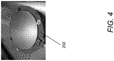
- the device wafer 20 is placed in the fixture chuck 202 (shown in FIG. 4 ) with the adhesive layer facing up.
- spacers 203 are placed on top of the device wafer 20 and then the carrier wafer 30 is placed on top of the spacers and the assembled fixture chuck 202 is transferred to the bonder module B 310.
- the chamber is evacuated, the spacers 203 are removed and the carrier wafer 30 is dropped onto the device wafer 20.
- a low force is applied by purging the chamber with a low pressure gas and the temperature is raised to 200 °C for the formation of the bond.
- the chamber is cooled and the fixture is unloaded.
- the Z-axis 239 moves up and the stacked wafers 20, 30 are brought into contact with the upper chuck 222.
- the upper chuck 222 may be semi-compliant or non-compliant, as will be described later.
- the debond process B 70b is a mechanical lift debond process and includes the following steps, shown in FIG. 2A .
- the bonded wafer stack 10 is mounted onto a dicing frame 25 (54) and the carrier wafer 30 is mechanically lifted away from the device wafer 20 (55).
- the thinned device wafer 20 remains supported by the dicing frame 25.
- temporary bond process C, 80a includes the following steps. First, a surface of the device wafer 20 is coated with an adhesive layer 23 (82). In one example, adhesive layer 23 is a UV curable adhesive LC3200TM, manufactured by 3M Company, MN, USA. The adhesive coated device wafer is then flipped (84). Next, a light absorbing release layer 33 is spin coated on a surface 30a of the carrier wafer 30 (86). In one example, light absorbing release layer 33 is a LC4000, manufactured by 3M Company, MN, USA.
- the flipped device wafer 20 is aligned with the carrier wafer 30 so that the surface 20a of the device wafer with the adhesive layer 23 is opposite to the surface 30a of the carrier wafer 30 with the light absorbing release layer.
- the two surfaces 20a and 30a are brought into contact and the adhesive layer is cured with UV light (87).
- the two wafers are bonded (88) in temporary bonder module C 410, shown in FIG. 3B .
- the bond is a temporary bond between the light absorbing release layer 33 and the adhesive layer 23 and is formed under vacuum of 0.1 mbar and low applied bond force.
- the temporary bonding (88) of the carrier wafer to the device wafer occurs in temporary module C, shown in FIG. 3B .
- the carrier wafer 30 with the laser absorbing release layer LTHC layer is placed on the top chuck 412 and held in place by holding pins 413.
- the device wafer 20 is placed on the bottom chuck 414 with the adhesive layer 23 facing up.
- the wafers 20, 30 are aligned, the chamber is evacuated, and the top chuck 412 with the carrier wafer 30 is dropped onto the device wafer 20.
- a low force is applied for the formation of the bond between the release layer 33 and the adhesive layer 23.
- the bonded wafer stack 10 is unloaded and the adhesive is cured with UV light.
- the debond process C 80b includes the following steps.
- the bonded wafer stack 10 is mounted onto a dicing frame 25 (56) and the carrier wafer 30 is illuminated with a YAG laser beam.
- the laser beam causes the separation of the wafer stack along the release layer 33 (57) and the separated carrier wafer 30 is mechanically lifted away from the device wafer 20 (58).
- the adhesive layer is peeled away from the device wafer surface 20a (59) and the thinned device wafer 20 remains supported by the dicing frame 25.
- temporary bonder cluster 110 includes a housing 101 having an upper cabinet structure 102 stacked on top of a lower cabinet 103.
- the upper cabinet 102 has a service access side 105 and the lower cabinet has leveling adjustments 104 and transport casters 106.
- the configurable temporary bond process modules 210, 310, 410, 510 are vertically stacked, as shown in FIG. 6 .
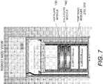
- Hot plate modules 130 and cold plate modules 140 are also vertically stacked on top, below or in-between the process modules 210, 310, as shown in FIG. 7 . Additional process modules may be included in order to provide further processing functionalities.
- Examples of the bond process modules include low applied force module, high applied force module, high temperature and low temperature modules, illumination (UV light or laser) modules, high pressure (gas) module, low (vacuum) pressure module and combinations thereof.
- temporary bond module 210 includes a housing 212 having a load door 211, an upper block assembly 220 and an opposing lower block assembly 230.
- the upper and lower block assemblies 220, 230 are movably connected to four Z-guide posts 242. In other embodiments, less than four or more than four Z-guide posts are used.
- a telescoping curtain seal 235 is disposed between the upper and lower block assemblies 220, 230.
- a temporary bonding chamber 202 is formed between the upper and lower assemblies 220, 230 and the telescoping curtain seal 235.
- the curtain seal 235 keeps many of the process components that are outside of the temporary bonding chamber area 202 insulated from the process chamber temperature, pressure, vacuum, and atmosphere.
- Process components outside of the chamber area 202 include guidance posts 242, Z-axis drive 243, illumination sources, mechanical pre-alignment arms 460a, 460b and wafer centering jaws 461a, 461b, among others.
- Curtain 235 also provides access to the bond chamber 202 from any radial direction.
- the lower block assembly 230 includes a heater plate 232 supporting the wafer 20, an insulation layer 236, a water cooled support flange 237 a transfer pin stage 238 and a Z-axis block 239.
- Heater plate 232 is a ceramic plate and includes resistive heater elements 233 and integrated air cooling 234. Heater elements 233 are arranged so the two different heating zones are formed.
- a first heating zone 233B is configured to heat a 200 mm wafer or the center region of a 300 mm wafer and a second heating zone 233A is configured to heat the periphery of the 300 mm wafer.
- Heating zone 233A is controlled independently from heating zone 233B in order to achieve thermal uniformity throughout the entire bond interface 405 and to mitigate thermal losses at the edges of the wafer stack.
- Heater plate 232 also includes two different vacuum zones for holding wafers of 200 mm and 300 mm, respectively.
- the water cooled thermal isolation support flange 237 is separated from the heater plate by the insulation layer 236.
- the transfer pin stage 238 is arranged below the lower block assembly 230 and is movable supported by the four posts 242. Transfer pin stage 238 supports transfer pins 240 arranged so that they can raise or lower different size wafers. In one example, the transfer pins 240 are arranged so that they can raise or lower 200 mm and 300 mm wafers.
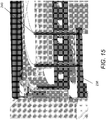
- Transfer pins 240 are straight shafts and, in some embodiments, have a vacuum feed opening extending through their center, as shown in FIG. 15 . Vacuum drawn through the transfer pin openings holds the supported wafers in place onto the transfer pins during movement and prevents misalignment of the wafers.
- the Z-axis block 239 includes a precision Z-axis drive 243 with ball screw, linear cam design, a linear encoder feedback 244 for submicron position control, and a servomotor 246 with a gearbox, shown in FIG. 12 .
- the upper block assembly 220 includes an upper ceramic chuck 222, a top static chamber wall 221 against which the curtain 235 seals with seal element 235a, a 200 mm and a 300 mm membrane layers 224a, 224b, and three metal flexure straps 226 arranged circularly at 120 degrees.
- the membrane layers 224a, 224b are clamped between the upper chuck 222 and the top housing wall 213 with clamps 215a, 215b, respectively, and form two separate vacuum zones 223a, 223b designed to hold 200 mm and 300 mm wafers, respectively, as shown in FIG. 14 .
- Membrane layers 224a, 224b are made of elastomer material or metal bellows.
- the top ceramic chuck 222 is highly flat and thin. It has low mass and is semi-compliant in order to apply uniform pressure upon the wafer stack 10.
- the top chuck 222 is lightly pre-loaded with membrane pressure against three adjustable leveling clamp/drive assemblies 216. Clamp/drive assemblies 216 are circularly arranged at 120 degrees.
- the top chuck 222 is initially leveled while in contact with the lower ceramic heater plate 232, so that it is parallel to the heater plate 232.
- the three metal straps 226 act a flexures and provide X-Y-T (Theta) positioning with minimal Z-constraint.
- the clamp/drive assemblies 216 also provide a spherical Wedge Error Compensating (WEC) mechanism that rotates and/or tilts the ceramic chuck 222 around a center point corresponding to the center of the supported wafer without translation.
- WEC spherical Wedge Error Compensating
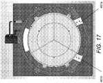
- Centering device 460 includes two pre-alignment arms 460a, 460b, shown in the open position in FIG. 16 and in the closed position in FIG. 17 .
- the mechanical jaws 461a, 461b have tapered surfaces 462 and 463 that conform to the curved edge of the 300 mm wafer and 200 mm wafer, respectively, as shown in FIG. 18A and FIG. 18B .
- Wafer centering device 470 includes three centering linkages 471, 472, 473.
- Centering linkage 471 includes a rectilinear mid-position air bearing or mechanical slide 471a that moves the wafer 30 in the Y-direction.
- Centering linkages 472, 473 include rotating centering arms 472a, 473a, that rotate clockwise and counterclockwise, respectively.
- the motions of the centering linkages 471, 472, 473 are synchronized by the use of a cam plate 474 with two linear cam profiles 474a, 474b.
- Cam profile 474a provides rectilinear motion for the mid-position centering arm 471 and cam profile 474b provides rectilinear motion for left and right centering arm push rods 472b, 473b.
- the rectilinear motion of the push rods 472b, 473b is translated into rotary motion at the cam/cam follower interface at the centering arms 472a, 473a, respectively.
- the cam plate is 474 fixed to a linear slide that is driven in a rectilinear motion (X-axis motion) by an electric motor or pneumatic actuation.
- a Linear Variable Differential Transformer (LVDT) or another electrical sensor at the mid-position centering arm 471 mechanism provides distance feedback, which indicates that the centering devices are stopped against the wafer edge.
- There is a spring preload on the centering device 471 a and when the spring preload is overtaken the LVDT registers a displacement.
- Wafer centering device 400 includes three centering linkages 481, 482, 483.
- Centering linkage 481 includes a rectilinear mid-position air bearing or mechanical slide 481a that moves the wafer 30 in the Y-direction.
- Centering linkages 482, 483, include rotating centering arms 482a, 483a, that rotate clockwise and counterclockwise, respectively, and push rods 482b, 483b.
- the motions of the centering linkages 481, 482, 483, are synchronized by the use of two plates 484, 485 that include linear cam profiles 484a, 484b, respectively.
- Cam profiles 484a, 485a provide rectilinear motion for left and right centering arm push rods 482b, 483b, respectively.
- the rectilinear motion of the push rods 482b, 483b is translated into rotary motion at the cam/cam follower interface at the centering arms 482a, 483a, respectively.
- Plates 484, 485 are connected to linear slide 481a via rods 481a, 481b, respectively.
- the linear motion of slide 481a in the Y direction is translated via the rods 481a, 481b, into linear motion of plates 484, 485, respectively, along the X-axis, as shown in FIG. 19D .
- the temporary bonding operation with the bonder module 210 includes the following steps.
- the non-adhesive substrate is loaded onto the transfer pins 240a by a robot end effector (350).
- the substrate is a 300 mm wafer and is supported by the 300 mm pins 240a, whereas the 200 mm pins 240b are shown to be slightly lower than the 300 mm pins 240a.
- the mechanical taper jaws 461a, 461b move into position around the wafer and the transfer pins 240a move down (352).
- the transfer pins have vacuum and purge functions.
- the purge function allows the wafer to float during the centering cycle and the vacuum function holds the wafer when the centering is complete.
- the tapered "funnel" jaws 461a, 461b, 461c drive the wafer to the center as it is lowered via the transfer pins 240a. Jaws 461a, 461b, 461c, are designed to accommodate and pre-align any size wafers, including 200 mm and 300mm, shown in FIG. 19 and 18 , respectively.
- the centering jaws 461a, 461b, 461c retract and the transfer pins move up to place the top substrate 20 on the upper vacuum chuck 222, as shown in FIG. 20C (354).
- a second adhesive coated substrate 30 is loaded face up onto the transfer pins 240a by the robot end effector (356), shown in FIG. 21A (356).
- the mechanical taper jaws 460 move into position around the wafer 30 and the transfer pins 240a move down and then up (358), shown in FIG. 21B .
- the centering jaws 461a, 461b retract and the transfer pins 240a move down to place the substrate 30 on the bottom vacuum chuck 232 (359), shown in FIG. 21C .
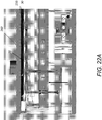
- the lower heater stage 230 moves up to form a close process gap between the top 20 and bottom 30 substrates and the curtain seal 235 is closed to form the temporary bonding chamber 202 (360), shown in FIG. 22A .
- An initial deep vacuum is drawn (10-4 mbar) in the temporary bonding chamber 202 while the top substrate with 20 is held via mechanical fingers.
- the chamber pressure is raised slightly to about 5mbar to generate a differential vacuum pressure that holds the top substrate 20 to the upper chuck 222.
- the Z-axis stage 239 moves further up to bring the bottom substrate 30 in contact with the top substrate 20, a shown in FIG. 22B (362).
- the top chuck 222 is lifted off from the stops 216 by this motion (362).
- force is applied via the top membrane 224a and bottom top chuck 232 and the wafer stack 10 are heated to the process temperature (364).
- the applied force is in the range between 500 N to 8000N and the process temperature is 200 C.
- the wafer stack 10 is compressed with the membrane pressure to ensure good thermal transfer. After the end of the treatment, the bonded wafer stack 10 is cooled and unloaded with the help of the transfer pins and the robot end effector (366).
- the Z-axis moves up to contact the thin, semi-compliant upper chuck 222/ membrane 224 design.
- the adhesive layer controls the TTV/tilt by applying pressure only in the direction perpendicular to the bond interface via the membranes/chuck flexures and by using a semi compliant chuck to conform to the adhesive topography.
- the Z-axis moves up to contact a non-compliant chuck.
- the Z-axis motion controls the final thickness of the adhesive layer and forces the adhesive to conform to the rigid flat chuck 222.
- the adhesive layer thickness may be controlled by using a Z-axis position control, pre-measured substrate thicknesses and known adhesive thicknesses.
- a compliant layer is installed on the bottom chuck 232 and the adhesive is pre-cured or its viscosity is adjusted.
- heat is applied both through the bottom and top chucks.
- thermal slide debonder 150 includes a top chuck assembly 151, a bottom chuck assembly 152, a static gantry 153 supporting the top chuck assembly 151, an X-axis carriage drive 154 supporting the bottom chuck assembly 152, a lift pin assembly 155 designed to raise and lower wafers of various diameters including diameters of 200 mm and 300 mm, and a base plate 163 supporting the X-axis carriage drive 154 and gantry 153.
- the top chuck assembly 151 includes a top support chuck 157 bolted to gantry 153, a heater support plate 158 in contact with the bottom surface of the top support chuck 157, a top heater 159 in contact with the bottom surface of the heater plate 158, a Z-axis drive 160 and a plate leveling system for leveling the upper wafer plate/ heater bottom surface 164.
- the plate leveling system includes three guide shafts 162 that connect the top heater 159 to the top support chuck 157 and three pneumatically actuated split clamps 161.
- the plate leveling system provides a spherical Wedge Error Compensating (WEC) mechanism that rotates and/or tilts the upper wafer plate 164 around a center point corresponding to the center of the supported wafer without translation.
- the heater 159 is a steady state heater capable to heat the supported wafer stack 10 up to 350 °C.
- Heater 159 includes a first heating zone configured to heat a 200 mm wafer or the center region of a 300 mm wafer and a second heating zone configured to heat the periphery of the 300 mm wafer.
- the first and second heating zones are controlled independently from each other in order to achieve thermal uniformity throughout the entire bond interface of the wafer stack and to mitigate thermal losses at the edges of the wafer stack.
- the heater support plate 158 is water cooled in order to provide thermal isolation and to prevent the propagation of any thermal expansion stresses that may be generated by the top heater 159.
- the bottom chuck 152 is made of a low thermal mass ceramic material and is designed to slide along the X-axis on top of the air bearing carriage drive 154.
- the carriage drive 154 is guided in this X-axis motion by two parallel lateral carriage guidance tracks 156.
- Bottom chuck 152 is also designed to rotate along its Z-axis 169.
- a Z-axis rotation by a small angle i.e., twisting
- the base plate 163 is vibration isolated.
- base plate is made of granite.
- base plate 156 has a honeycomb structure and is supported by pneumatic vibration isolators (not shown).
- the debonding operation with the thermal slide debonder 150 of FIG. 23 includes the following steps. First, the temporary bonded wafer stack 10 is loaded on the primary lift pins 155 arranged so that the carrier wafer 30 is on the top and the thinned device wafer 20 is on the bottom (171). Next, the wafer stack 10 is lowered so that the bottom surface of the thinned device wafer 20 is brought into contact with the bottom chuck 152 (172). The bottom chuck 152 is then moved along the 165a direction until it is under the top heater 159 (174).
- the Z-axis 160 of the top chuck 151 moves down and the bottom surface 164 of the top heater159 is brought into contact with the top surface of the carrier wafer 30 and then air is floated on top heater 159 and carrier wafer 30 until the carrier wafer stack 30 reaches a set temperature.
- the set temperature is reached, vacuum is pulled on the carrier wafer 30 so that is held by the top chuck assembly 151 and the guide shafts 162 are locked in the split clamps 162 (175).
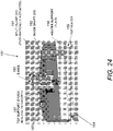
- top chuck 151 is rigidly held while the bottom chuck 152 is compliant and the thermal slide separation is initiated (176) by first twisting the bottom chuck 152 and then moving the X-axis carriage 154 toward the 165b direction away from the rigidly held top chuck assembly 151 (177).
- the debonded thinned device wafer 20 is carried by the X-axis carriage 154 to the unload position where it is lifted up by the pins (178) for removal (179).
- the X-axis carriage 154 moves back along direction 165a (180).
- the lift pins 155 Upon reaching the position under the top chuck assembly 151, the lift pins 155 are raised to contact the adhesive side of the carrier wafer 30 and air is purged onto the heater plate 159 to release the carrier wafer from it (181). The lift pins 155 are lowered to a height just above the bottom chuck plane so as to not contaminated the bottom chuck top surface with the adhesive (182) and the X-axis carriage 154 moves along 165b back to the unload position. The carrier wafer is cooled and then removed (183).
- the bottom chuck 152 is supported by a Z-stage 501 and support arms 502a, 502b and 502c.
- the thinned wafer pair 10 is placed on top of bottom chuck 152 with the thinned device wafer 20 being in contact with the bottom chuck 152 and the carrier wafer 30 facing the top chuck assembly 151.
- the Z-stage 501 is preloaded with a small force F1 503 pulling the bottom chuck 152 down in the direction 504 to a distance of about 0.5 mm from the center of the thinned wafer 20.
- top chuck 151 is rigidly held while the bottom chuck 152 is compliant in the Z-direction 504 (while being laterally stiff in the 165a direction) and the thermal slide separation is initiated (176) by first twisting the bottom chuck 152 and then pulling the Z-stage 501 toward the 165b direction away from the rigidly held top chuck assembly 151 (177).
- a load cell 506 (shown in FIG. 25 ) measures the horizontal force F2 505 that pulls the Z-stage 501 and therefore it measures the resistance of the debonding force.
- Horizontal force F2 505 may be maintained constant or varied by controlling the velocity of the X-axis motion.
- a 200 mm wafer is pulled in the X-direction 165b with a traverse velocity of about 2 mm/sec for a distance of about 50mm.
- the traverse velocity is increased to 4 mm/sec for a distance of about 75 mm and then the traversed velocity is increased to 6mm/sec for distance of 75 mm.
- the wafer is also twisted with a rotational velocity of 0.5 degrees per second for about 30 degrees.
- the wafer pair 10 is preheated prior to the debonding step to prevent thermal shock.
- mechanical debonder B 250 debonds the carrier wafer 30 from the thinned device wafer 20 by mechanically lifting an edge 31 of the carrier wafer 30 away from the thinned device wafer 20.
- the temporary bonded wafer stack 10 Prior to the debonding process the temporary bonded wafer stack 10 is attached to a frame 25, and upon separation the thinned wafer remains supported by the frame 25.
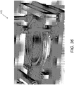
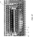
- debonder 250 includes a flex plate 253 with a two zone circular vacuum seal 255. Seal 255 includes two zones, one for a sealing a 200 mm wafer placed within the area surrounded by the seal and a second for sealing a 300 mm wafer within the area surrounded by the seal.
- Seal 255 is implemented either with an O-ring or with suction cups.
- a lift pin assembly 254 is used to raise or lower the separated carrier wafer 30 that is transported by the flex plate 253.
- Debonder 250 also includes a vacuum chuck 256. Both the vacuum chuck 256 and the flex plate 253 are arranged next to each other upon a support plate 152, which in turn is supported by the base plate 251. Flex plate 253 has an edge 253b connected to a hinge 263 that is driven by a hinge motor drive 257.
- Vacuum chuck 256 is made of a porous sintered ceramic material and is designed to support the separated thin wafer 20.
- Hinge motor drive 257 is used to drive the flex plate 253 upon the wafer stack 10 after the wafer stack 10 has been loaded on the vacuum chuck 256.
- An anti-backlash gear drive 258 is used to prevent accidental backing of the flex plate 253.
- a debond drive motor 259 is attached at the edge 251a of the base plate 251 and next to the edge of the chuck support plate 252a. Debond drive motor 259 moves a contact roller 260 vertical to the plane of the base plate 251 in direction 261 and this motion of the contact roller 260 lifts the edge 253a of the flex plate 253 after the flex plate has been placed upon the loaded wafer stack 10, as will be described below.
- the debonding operation 270 with the debonder 250 includes the following steps. First, The tape frame 25 with the wafer stack 10 is loaded upon the vacuum chuck 256, so that the carrier wafer 30 is on the top and the thinned wafer 20 is on the bottom (271). The tape frame 25 is indexed against the frame registration pins 262, shown in FIG. 28 , and the position of the tape frame 25 is locked. Next, vacuum is pulled through the porous vacuum chuck 256 to hold the tape frame adhesive film. Next, the hinge motor 257 is engaged to transport the flex plate 253 onto the loaded wafer stack, so that it is in contact with the back of the carrier wafer 30 (272).
- the carrier wafer 30 is fabricated on a (110) plane so that its 110 direction is perpendicular to the push direction 261a, thereby preventing breaking of the wafer 30 during delamination.
- the thinned wafer 20 remains attached to the tape frame 25, which is held by the vacuum chuck 256.
- the debond motor 259 is held constant in position.
- the hinge motor drive 257 opens the flex plate 253 with the attached separated carrier wafer 30 in the "open position", in a controlled manner (274).
- the flex plate vacuum is released thereby releasing the carrier wafer 30.
- the lift pins 254 are moved up to raise the carrier wafer 30 oriented so that the release layer 32 is facing up and then the carrier wafer 30 is removed.
- the vacuum through the porous vacuum chuck 256 is released and the tape 25 with the attached thinned wafer 20 is removed.
- a resistance roller 610 is used to apply a downward force upon flex plate 253 while contact roller 260 pushes up and lifts the edge 253a of the flex plate 253.
- the bonded wafer pair 10 and the debonded device wafer 20 and carrier wafer 30 are loaded and removed from the debonder from the same direction 620.
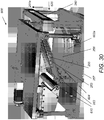
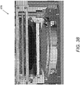
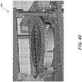
- Debonder 600 includes a flex plate 253 with multi-zone circular vacuum seals 255. Seals 255 include at least two zones, one for a sealing a 200 mm wafer placed within the area surrounded by the seal and a second for sealing a 300 mm wafer within the area surrounded by the seal, among others.
- Debonder 600 also includes a vacuum chuck 256, a lift pin assembly 604 and transfer arms 602a, 602b, 602c. In this case the lift pin assembly 604 and transfer arms 602a, 602b, 602c are located around vacuum chuck 256, as shown in FIG. 30 .
- Flex plate 253 has an edge 253b connected to a hinge 263 that is driven by a hinge motor drive 257.
- Vacuum chuck 256 is made of a porous sintered ceramic material and is designed to support the bonded wafer pair 10 and the separated thin wafer 20 and carrier wafer 30.
- Hinge motor drive 257 is used to drive the flex plate 253 upon the wafer stack 10 after the wafer stack 10 has been loaded on the vacuum chuck 256.
- An anti-backlash gear drive 258 is used to prevent accidental backing of the flex plate 253 (shown in FIG. 28 ).
- a debond drive motor 259 is attached at the edge 251a of the base plate 251 and next to the edge of the chuck support plate 252a (shown in FIG. 28 ). Debond drive motor 259 moves a contact roller 260 vertical to the plane of the base plate 251 in direction 261a and this motion of the contact roller 260 lifts the edge 253a of the flex plate 253 after the flex plate has been placed upon the loaded wafer stack 10, as will be described below.
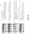
- the debonding operation with the debonder 600 includes the following steps. First, the tape frame 25 with the wafer stack 10 is loaded on the vacuum chuck 256, so that the carrier wafer 30 is on the top and the thinned wafer 20 is on the bottom (662). The tape frame 25 is indexed against the frame registration pins 262, and the position of the tape frame 25 is locked. Next, vacuum is pulled through the porous vacuum chuck 256 to hold the tape frame adhesive film. Next, the hinge motor 257 is engaged to lower the flex plate 253 onto the loaded wafer stack 10, so that it is in contact with the back of the carrier wafer 30 (664).
- the flex plate 253 with the attached separated carrier wafer 30 is raised with the hinge motor 257 and the thinned device wafer 20 remains attached to the tape frame 25, which is held by the vacuum chuck 256 (674).
- the vacuum through the porous vacuum chuck 256 is released and the tape 25 with the attached thinned wafer 20 is unloaded from the direction 620 (676).
- the transfer arms 602a, 602b, 602c are inserted on chuck 256 (678) and the flex-plate 253 with the carrier wafer 30 is lowered onto the transfer arms 602a, 602b, 602c (680).
- the vacuum seal is released and the carrier wafer 30 is separated from the flex-plate 253 (682).
- the carrier wafer 30 is unloaded from the chuck 256, also from direction 620 (684).
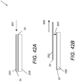
- the separation of the bonded wafer stack 10 is initiated by pushing the flex-plate 253 with the carrier wafer 30 horizontally along direction 691, as shown in FIG. 42A , or moving the flex-plate 253 horizontally along direction 692 while pushing down 693 the device wafer edge, as shown in FIG. 42B .
- the apparatus does not include a hinge motor drive 257, and hinge 263 is manually driven.
- the apparatus does not include a debond drive motor 259 and the actuation of contact roller 260 is driven pneumatically via a piston and a proportional regulator.
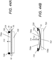
- a new debonder apparatus 700 includes un upper chuck 730 and a lower chuck 720 contained within a clam-cell type reactor having a lower portion 702 and top cover portion 704. Two separate chambers 706 and 708 are formed within the reactor 700 with lower chamber 706 containing the lower chuck 720 and upper chamber 708 containing the upper chuck 730. The lower surface 730a of the upper chuck protrudes into lower chamber 706. Upper and lower chucks 730,720 are porous ceramics and vacuum is drawn through them making them capable to apply a force along directions 712, 714, respectively, shown in FIG. 44C .
- Forces 712, 714 are applied throughout the lower surface 730a and upper surface 720a of upper and lower chucks 730 and 720, respectively. Forces 712, 714 are used for holding substrates by the upper or lower chucks 730 and 720, respectively.
- Upper and lower chambers 708, 706 are configured to be filled with a pressurized gas.
- the pressurized gas applies pressure 711 on the upper surface 730b of the upper chuck 730 or pressure 716 the top surface 720a of the lower chuck 720.
- pressure 711 and 716 is about 2 bars and the pressurized gas is nitrogen.
- the outer edges of the upper chuck 730 are held in a fixed position by clamps 725 while pressure 711 is applied.
- Clamps 725 may be mechanical clamps or vacuum clamps.
- the bonded wafer pair 10 supported on the tape frame 25 is loaded in chamber 708 and is held via vacuum force 712 in contact with the lower surface 730a of the upper chuck 730, shown in FIG. 44A .
- Vacuum force 712 is applied in the entire unbonded surface of wafer 30.
- Next chamber 708 is filled with gas and pressure 711 is applied on the back surface 730b of chuck 730 by the pressurized gas while the edges of the chuck 730 are held fixed by clamps 725. This causes the lower surface 730a of chuck 730 and the attached bonded wafer pair 10 to bow downward until it contacts the upper surface 720a of the lower chuck 720 in point 721, shown in FIG. 44B .
- separation of the bonded wafer pair 10 is initiated around point 10a.
- the separation is initiated via mechanical means, i.e., pushing up of frame 25 or pushing of the carrier wafer 30 sidewise. In other embodiments, the separation is initiated via an air knife.
- vacuum is drawn through the lower chuck 720 applying a vacuum force 714 on the lower surface of the wafer pair 10, shown in FIG. 44C .
- the pressure 711 in chamber 708 is reduced causing gradual removal of the downward bowing of the lower chuck surface 730a and the attached wafer pair 10.
- the pressure 716 in the lower chamber 706 is increased. The combination of these steps causes the propagation of the separation front that was initiated in point 10a, throughout the entire bond interface, as shown in FIG. 44D .
- pressure 711 is turned off, vacuum force 712 is turned off and then pressure 716 is turned off leaving the separated carrier wafer 30 and thinned device wafer 20 supported upon tape frame 25 on the lower chuck 720, where they are held by vacuum force 714, as shown in FIG. 44E .
Landscapes
- Engineering & Computer Science (AREA)
- Physics & Mathematics (AREA)
- Condensed Matter Physics & Semiconductors (AREA)
- General Physics & Mathematics (AREA)
- Manufacturing & Machinery (AREA)
- Computer Hardware Design (AREA)
- Microelectronics & Electronic Packaging (AREA)
- Power Engineering (AREA)
- Container, Conveyance, Adherence, Positioning, Of Wafer (AREA)
- Mechanical Treatment Of Semiconductor (AREA)
Priority Applications (1)
| Application Number | Priority Date | Filing Date | Title |
|---|---|---|---|
| EP12191692.8A EP2575163B1 (en) | 2010-04-16 | 2011-04-15 | Improved debonding equipment and methods for debonding temporary bonded wafers |
Applications Claiming Priority (3)
| Application Number | Priority Date | Filing Date | Title |
|---|---|---|---|
| US32488810P | 2010-04-16 | 2010-04-16 | |
| US13/087,137 US8551291B2 (en) | 2010-04-15 | 2011-04-14 | Debonding equipment and methods for debonding temporary bonded wafers |
| PCT/US2011/032607 WO2011130586A2 (en) | 2010-04-16 | 2011-04-15 | Improved debonding equipment and methods for debonding temporary bonded wafers |
Related Child Applications (3)
| Application Number | Title | Priority Date | Filing Date |
|---|---|---|---|
| EP12191692.8A Division-Into EP2575163B1 (en) | 2010-04-16 | 2011-04-15 | Improved debonding equipment and methods for debonding temporary bonded wafers |
| EP12191692.8A Division EP2575163B1 (en) | 2010-04-16 | 2011-04-15 | Improved debonding equipment and methods for debonding temporary bonded wafers |
| EP12191692.8 Division-Into | 2012-11-07 |
Publications (3)
| Publication Number | Publication Date |
|---|---|
| EP2559057A2 EP2559057A2 (en) | 2013-02-20 |
| EP2559057A4 EP2559057A4 (en) | 2016-11-30 |
| EP2559057B1 true EP2559057B1 (en) | 2018-01-24 |
Family
ID=81075156
Family Applications (2)
| Application Number | Title | Priority Date | Filing Date |
|---|---|---|---|
| EP12191692.8A Active EP2575163B1 (en) | 2010-04-16 | 2011-04-15 | Improved debonding equipment and methods for debonding temporary bonded wafers |
| EP11769635.1A Active EP2559057B1 (en) | 2010-04-16 | 2011-04-15 | Improved debonding equipment and methods for debonding temporary bonded wafers |
Family Applications Before (1)
| Application Number | Title | Priority Date | Filing Date |
|---|---|---|---|
| EP12191692.8A Active EP2575163B1 (en) | 2010-04-16 | 2011-04-15 | Improved debonding equipment and methods for debonding temporary bonded wafers |
Country Status (4)
| Country | Link |
|---|---|
| US (2) | US8366873B2 (zh) |
| EP (2) | EP2575163B1 (zh) |
| JP (2) | JP5868947B2 (zh) |
| WO (1) | WO2011130586A2 (zh) |
Families Citing this family (47)
| Publication number | Priority date | Publication date | Assignee | Title |
|---|---|---|---|---|
| US8950459B2 (en) * | 2009-04-16 | 2015-02-10 | Suss Microtec Lithography Gmbh | Debonding temporarily bonded semiconductor wafers |
| DE102009018156B4 (de) * | 2009-04-21 | 2024-08-29 | Ev Group Gmbh | Vorrichtung und Verfahren zum Trennen eines Substrats von einem Trägersubstrat |
| JP5374462B2 (ja) * | 2010-08-23 | 2013-12-25 | 東京エレクトロン株式会社 | 剥離システム、剥離方法、プログラム及びコンピュータ記憶媒体 |
| US8845859B2 (en) * | 2011-03-15 | 2014-09-30 | Sunedison Semiconductor Limited (Uen201334164H) | Systems and methods for cleaving a bonded wafer pair |
| CN103460369B (zh) | 2011-04-11 | 2016-12-28 | Ev 集团 E·索尔纳有限责任公司 | 柔性的承载支架、用于使承载基底脱离的装置以及方法 |
| US8945329B2 (en) * | 2011-06-24 | 2015-02-03 | Ibiden Co., Ltd. | Printed wiring board and method for manufacturing printed wiring board |
| US8261804B1 (en) * | 2011-10-28 | 2012-09-11 | Meicer Semiconductor Inc. | IC layers separator |
| JP5913053B2 (ja) * | 2011-12-08 | 2016-04-27 | 東京エレクトロン株式会社 | 剥離装置、剥離システム、剥離方法、プログラム及びコンピュータ記憶媒体 |
| EP2795669B1 (de) | 2011-12-22 | 2020-06-17 | EV Group E. Thallner GmbH | Biegsame substrathalterung, vorrichtung und verfahren zum lösen eines ersten substrats |
| JP2013147621A (ja) * | 2012-01-23 | 2013-08-01 | Nitto Denko Corp | 貼り合わされた2枚の板の分離方法 |
| US8696864B2 (en) | 2012-01-26 | 2014-04-15 | Promerus, Llc | Room temperature debonding composition, method and stack |
| JP5687647B2 (ja) * | 2012-03-14 | 2015-03-18 | 株式会社東芝 | 半導体装置の製造方法、半導体製造装置 |
| JP5591859B2 (ja) * | 2012-03-23 | 2014-09-17 | 株式会社東芝 | 基板の分離方法及び分離装置 |
| US8697542B2 (en) | 2012-04-12 | 2014-04-15 | The Research Foundation Of State University Of New York | Method for thin die-to-wafer bonding |
| US9111982B2 (en) | 2012-04-25 | 2015-08-18 | Taiwan Semiconductor Manufacturing Company, Ltd. | Wafer assembly with carrier wafer |
| WO2014006562A1 (en) * | 2012-07-03 | 2014-01-09 | Element Six Technologies Us Corporation | Handle for semiconductor-on-diamond wafers and method of manufacture |
| JP5806185B2 (ja) * | 2012-09-07 | 2015-11-10 | 東京エレクトロン株式会社 | 剥離システム |
| JP5870000B2 (ja) * | 2012-09-19 | 2016-02-24 | 東京エレクトロン株式会社 | 剥離装置、剥離システムおよび剥離方法 |
| US10000675B2 (en) * | 2013-03-03 | 2018-06-19 | John Cleaon Moore | Temporary adhesive with tunable adhesion force sufficient for processing thin solid materials |
| JP5909453B2 (ja) * | 2013-03-07 | 2016-04-26 | 東京エレクトロン株式会社 | 剥離装置、剥離システムおよび剥離方法 |
| KR102070087B1 (ko) * | 2013-04-29 | 2020-01-30 | 삼성전자주식회사 | 반도체 소자 제조방법 |
| US9269603B2 (en) * | 2013-05-09 | 2016-02-23 | Globalfoundries Inc. | Temporary liquid thermal interface material for surface tension adhesion and thermal control |
| TWI545019B (zh) * | 2013-10-28 | 2016-08-11 | 鴻海精密工業股份有限公司 | 撕膜機構 |
| US9523158B2 (en) * | 2014-02-07 | 2016-12-20 | Applied Materials, Inc. | Methods and apparatus for forming semiconductor |
| JP7071118B2 (ja) * | 2014-08-19 | 2022-05-18 | ルミレッズ ホールディング ベーフェー | ダイレベルのレーザリフトオフ中の機械的損傷を減少させるサファイアコレクタ |
| KR102305505B1 (ko) | 2014-09-29 | 2021-09-24 | 삼성전자주식회사 | 웨이퍼 서포팅 시스템 디본딩 이니시에이터 및 웨이퍼 서포팅 시스템 디본딩 방법 |
| EP3295479B1 (en) * | 2015-05-13 | 2018-09-26 | Lumileds Holding B.V. | Sapphire collector for reducing mechanical damage during die level laser lift-off |
| CN104979262B (zh) * | 2015-05-14 | 2020-09-22 | 浙江中纳晶微电子科技有限公司 | 一种晶圆分离的方法 |
| US20170001427A1 (en) * | 2015-07-02 | 2017-01-05 | Apple Inc. | Electronic Devices With Moisture And Light Curable Adhesive |
| TWI701708B (zh) | 2016-02-24 | 2020-08-11 | 德商蘇士微科技印刷術股份有限公司 | 半導體接合設備及相關技術 |
| USD815159S1 (en) * | 2016-05-16 | 2018-04-10 | Cost Effective Equipment Llc | Mechanical debonder |
| US10155369B2 (en) * | 2016-11-29 | 2018-12-18 | Taiwan Semiconductor Manufacturing Co., Ltd. | Wafer debonding system and method |
| CN106783699A (zh) * | 2017-03-03 | 2017-05-31 | 爱立发自动化设备(上海)有限公司 | 一种晶圆与玻璃分离装置及方法 |
| CN109560004A (zh) * | 2017-09-26 | 2019-04-02 | 天津环鑫科技发展有限公司 | 一种自动圆形硅片插片机构 |
| US10170443B1 (en) * | 2017-11-28 | 2019-01-01 | International Business Machines Corporation | Debonding chips from wafer |
| CN108155270B (zh) * | 2017-12-13 | 2019-09-20 | 北京创昱科技有限公司 | 一种薄膜与晶片的分离装置和分离方法 |
| EP3867047A1 (en) | 2018-10-15 | 2021-08-25 | General Electric Company | Systems and methods of automated film removal |
| CN109273389B (zh) * | 2018-11-01 | 2024-06-14 | 苏州展德自动化设备有限公司 | 晶圆保护纸自动剥离设备 |
| US20220010116A1 (en) | 2018-11-14 | 2022-01-13 | Denka Company Limited | Composition |
| WO2020140034A1 (en) * | 2018-12-28 | 2020-07-02 | Didi Research America, Llc | System and methods for microfabrication |
| JP7146354B2 (ja) * | 2019-01-22 | 2022-10-04 | 株式会社ディスコ | キャリア板の除去方法 |
| CH715871B1 (de) * | 2019-02-21 | 2023-10-13 | Smartpetcare Ag | Vorrichtung, insbesondere Haustierfütterungsvorrichtung und Verfahren zum Bereitstellen und Öffnen gefüllter Behälter. |
| KR102640172B1 (ko) | 2019-07-03 | 2024-02-23 | 삼성전자주식회사 | 기판 처리 장치 및 이의 구동 방법 |
| EP4148096A4 (en) | 2020-05-21 | 2023-11-01 | Denka Company Limited | COMPOSITION |
| CN112216632B (zh) * | 2020-09-24 | 2024-04-19 | 广东海信宽带科技有限公司 | 一种ld芯片共晶焊接台 |
| CN117242146A (zh) | 2021-04-26 | 2023-12-15 | 电化株式会社 | 组合物 |
| TWI812550B (zh) * | 2022-11-24 | 2023-08-11 | 天虹科技股份有限公司 | 鍵合基板的分離方法 |
Family Cites Families (38)
| Publication number | Priority date | Publication date | Assignee | Title |
|---|---|---|---|---|
| US4046985A (en) * | 1974-11-25 | 1977-09-06 | International Business Machines Corporation | Semiconductor wafer alignment apparatus |
| JP3318615B2 (ja) * | 1994-02-09 | 2002-08-26 | 明治機械株式会社 | 研磨機におけるワ−クの取外し方法 |
| JPH0964152A (ja) * | 1995-08-24 | 1997-03-07 | Mimasu Handotai Kogyo Kk | ウェーハ単離装置 |
| KR0165467B1 (ko) * | 1995-10-31 | 1999-02-01 | 김광호 | 웨이퍼 디본더 및 이를 이용한 웨이퍼 디본딩법 |
| JPH10244545A (ja) * | 1997-03-04 | 1998-09-14 | Canon Inc | 離型方法及び離型装置 |
| CA2232796C (en) * | 1997-03-26 | 2002-01-22 | Canon Kabushiki Kaisha | Thin film forming process |
| US6540861B2 (en) * | 1998-04-01 | 2003-04-01 | Canon Kabushiki Kaisha | Member separating apparatus and processing apparatus |
| US6221740B1 (en) * | 1999-08-10 | 2001-04-24 | Silicon Genesis Corporation | Substrate cleaving tool and method |
| DE10008111A1 (de) * | 2000-02-22 | 2001-08-23 | Krauss Maffei Kunststofftech | Vorrichtung zum Vakuumpressen von DVD-Substraten |
| WO2002056352A1 (fr) * | 2001-01-15 | 2002-07-18 | Lintec Corporation | Appareil d'assemblage et procede d'assemblage |
| JP2002237515A (ja) * | 2001-02-07 | 2002-08-23 | Mitsubishi Gas Chem Co Inc | 薄葉化半導体基板の剥離装置および剥離法 |
| DE10128924A1 (de) | 2001-06-15 | 2003-01-23 | Philips Corp Intellectual Pty | Verfahren zum Umsetzen eines im wesentlichen scheibenförmigen Werkstücks sowie Vorrichtung zum Durchführen dieses Verfahrens |
| JP3737059B2 (ja) * | 2002-03-14 | 2006-01-18 | 芝浦メカトロニクス株式会社 | 基板貼り合わせ装置および基板貼り合わせ方法 |
| JP4565804B2 (ja) * | 2002-06-03 | 2010-10-20 | スリーエム イノベイティブ プロパティズ カンパニー | 被研削基材を含む積層体、その製造方法並びに積層体を用いた極薄基材の製造方法及びそのための装置 |
| US7187162B2 (en) * | 2002-12-16 | 2007-03-06 | S.O.I.Tec Silicon On Insulator Technologies S.A. | Tools and methods for disuniting semiconductor wafers |
| JP4614626B2 (ja) * | 2003-02-05 | 2011-01-19 | 東京エレクトロン株式会社 | 薄肉半導体チップの製造方法 |
| JP2005039114A (ja) * | 2003-07-17 | 2005-02-10 | Disco Abrasive Syst Ltd | 半導体ウェーハ移し替え装置 |
| FR2860178B1 (fr) * | 2003-09-30 | 2005-11-04 | Commissariat Energie Atomique | Procede de separation de plaques collees entre elles pour constituer une structure empilee. |
| US20050150597A1 (en) * | 2004-01-09 | 2005-07-14 | Silicon Genesis Corporation | Apparatus and method for controlled cleaving |
| JP2006021849A (ja) * | 2004-07-06 | 2006-01-26 | Central Glass Co Ltd | 薄板ガラスの搬送装置及び搬送方法 |
| KR101278460B1 (ko) | 2005-03-01 | 2013-07-02 | 다우 코닝 코포레이션 | 반도체 가공을 위한 임시 웨이퍼 접착방법 |
| JP4666514B2 (ja) | 2006-07-20 | 2011-04-06 | リンテック株式会社 | シート剥離装置及び剥離方法 |
| JP4822989B2 (ja) | 2006-09-07 | 2011-11-24 | 日東電工株式会社 | 基板貼合せ方法およびこれを用いた装置 |
| US20080200011A1 (en) | 2006-10-06 | 2008-08-21 | Pillalamarri Sunil K | High-temperature, spin-on, bonding compositions for temporary wafer bonding using sliding approach |
| US20080302481A1 (en) | 2007-06-07 | 2008-12-11 | Tru-Si Technologies, Inc. | Method and apparatus for debonding of structures which are bonded together, including (but not limited to) debonding of semiconductor wafers from carriers when the bonding is effected by double-sided adhesive tape |
| JP4729003B2 (ja) * | 2007-06-08 | 2011-07-20 | リンテック株式会社 | 脆質部材の処理方法 |
| JP4733074B2 (ja) | 2007-06-11 | 2011-07-27 | リンテック株式会社 | 分離装置及び分離方法 |
| KR100891384B1 (ko) * | 2007-06-14 | 2009-04-02 | 삼성모바일디스플레이주식회사 | 플렉서블 기판 접합 및 탈착장치 |
| CN101779268B (zh) | 2007-06-25 | 2013-11-06 | 布鲁尔科技公司 | 高温旋涂暂时性粘合组合物 |
| US8101981B2 (en) | 2007-08-10 | 2012-01-24 | Array Optronix, Inc. | Back-illuminated, thin photodiode arrays with isolating etched trenches between elements |
| US20090174018A1 (en) | 2008-01-09 | 2009-07-09 | Micron Technology, Inc. | Construction methods for backside illuminated image sensors |
| US9111981B2 (en) | 2008-01-24 | 2015-08-18 | Brewer Science Inc. | Method for reversibly mounting a device wafer to a carrier substrate |
| DE102008018536B4 (de) * | 2008-04-12 | 2020-08-13 | Erich Thallner | Vorrichtung und Verfahren zum Aufbringen und/oder Ablösen eines Wafers auf einen/von einem Träger |
| US7960840B2 (en) | 2008-05-12 | 2011-06-14 | Texas Instruments Incorporated | Double wafer carrier process for creating integrated circuit die with through-silicon vias and micro-electro-mechanical systems protected by a hermetic cavity created at the wafer level |
| JP4740298B2 (ja) * | 2008-09-04 | 2011-08-03 | リンテック株式会社 | シート剥離装置及び剥離方法 |
| KR20120027237A (ko) * | 2009-04-16 | 2012-03-21 | 수스 마이크로텍 리소그라피 게엠바하 | 웨이퍼 가접합 및 분리를 위한 개선된 장치 |
| US8435804B2 (en) * | 2010-12-29 | 2013-05-07 | Gtat Corporation | Method and apparatus for forming a thin lamina |
| US8657994B2 (en) * | 2011-04-01 | 2014-02-25 | Alta Devices, Inc. | System and method for improved epitaxial lift off |
-
2011
- 2011-04-12 US US13/085,159 patent/US8366873B2/en active Active
- 2011-04-14 US US13/087,137 patent/US8551291B2/en active Active
- 2011-04-15 EP EP12191692.8A patent/EP2575163B1/en active Active
- 2011-04-15 EP EP11769635.1A patent/EP2559057B1/en active Active
- 2011-04-15 WO PCT/US2011/032607 patent/WO2011130586A2/en active Application Filing
- 2011-04-15 JP JP2013505163A patent/JP5868947B2/ja active Active
-
2016
- 2016-01-06 JP JP2016001072A patent/JP6162829B2/ja not_active Expired - Fee Related
Non-Patent Citations (1)
| Title |
|---|
| None * |
Also Published As
| Publication number | Publication date |
|---|---|
| JP6162829B2 (ja) | 2017-07-12 |
| JP2013526021A (ja) | 2013-06-20 |
| EP2559057A4 (en) | 2016-11-30 |
| JP5868947B2 (ja) | 2016-02-24 |
| WO2011130586A3 (en) | 2012-04-19 |
| EP2559057A2 (en) | 2013-02-20 |
| EP2575163B1 (en) | 2019-08-21 |
| JP2016106404A (ja) | 2016-06-16 |
| US8366873B2 (en) | 2013-02-05 |
| US8551291B2 (en) | 2013-10-08 |
| EP2575163A3 (en) | 2017-12-27 |
| EP2575163A2 (en) | 2013-04-03 |
| US20110253315A1 (en) | 2011-10-20 |
| WO2011130586A2 (en) | 2011-10-20 |
| US20110253314A1 (en) | 2011-10-20 |
Similar Documents
| Publication | Publication Date | Title |
|---|---|---|
| EP2559057B1 (en) | Improved debonding equipment and methods for debonding temporary bonded wafers | |
| US9281229B2 (en) | Method for thermal-slide debonding of temporary bonded semiconductor wafers | |
| US8343300B2 (en) | Automated thermal slide debonder | |
| US9064686B2 (en) | Method and apparatus for temporary bonding of ultra thin wafers | |
| EP2577720B1 (en) | Apparatus and method for detaping an adhesive layer from the surface of ultra thin wafers | |
| WO2003012873A1 (fr) | Procede de fabrication de plaquettes soi et gabarit de separation de plaquettes |
Legal Events
| Date | Code | Title | Description |
|---|---|---|---|
| PUAI | Public reference made under article 153(3) epc to a published international application that has entered the european phase |
Free format text: ORIGINAL CODE: 0009012 |
|
| 17P | Request for examination filed |
Effective date: 20121114 |
|
| AK | Designated contracting states |
Kind code of ref document: A2 Designated state(s): AL AT BE BG CH CY CZ DE DK EE ES FI FR GB GR HR HU IE IS IT LI LT LU LV MC MK MT NL NO PL PT RO RS SE SI SK SM TR |
|
| RAP1 | Party data changed (applicant data changed or rights of an application transferred) |
Owner name: SUESS MICROTEC LITHOGRAPHY GMBH |
|
| DAX | Request for extension of the european patent (deleted) | ||
| RAP1 | Party data changed (applicant data changed or rights of an application transferred) |
Owner name: SUSS MICROTEC LITHOGRAPHY GMBH |
|
| A4 | Supplementary search report drawn up and despatched |
Effective date: 20161103 |
|
| RIC1 | Information provided on ipc code assigned before grant |
Ipc: H01L 21/683 20060101ALI20161027BHEP Ipc: H01L 21/20 20060101AFI20161027BHEP Ipc: H01L 21/67 20060101ALI20161027BHEP Ipc: H01L 21/68 20060101ALI20161027BHEP Ipc: B32B 38/18 20060101ALN20161027BHEP Ipc: B32B 43/00 20060101ALN20161027BHEP |
|
| GRAP | Despatch of communication of intention to grant a patent |
Free format text: ORIGINAL CODE: EPIDOSNIGR1 |
|
| RIC1 | Information provided on ipc code assigned before grant |
Ipc: H01L 21/67 20060101ALI20170706BHEP Ipc: B32B 43/00 20060101ALN20170706BHEP Ipc: H01L 21/683 20060101ALI20170706BHEP Ipc: H01L 21/20 20060101AFI20170706BHEP Ipc: B32B 38/18 20060101ALN20170706BHEP Ipc: H01L 21/68 20060101ALI20170706BHEP |
|
| INTG | Intention to grant announced |
Effective date: 20170728 |
|
| RIC1 | Information provided on ipc code assigned before grant |
Ipc: B32B 38/18 20060101ALN20170717BHEP Ipc: H01L 21/67 20060101ALI20170717BHEP Ipc: B32B 43/00 20060101ALN20170717BHEP Ipc: H01L 21/20 20060101AFI20170717BHEP Ipc: H01L 21/683 20060101ALI20170717BHEP Ipc: H01L 21/68 20060101ALI20170717BHEP |
|
| GRAS | Grant fee paid |
Free format text: ORIGINAL CODE: EPIDOSNIGR3 |
|
| GRAA | (expected) grant |
Free format text: ORIGINAL CODE: 0009210 |
|
| AK | Designated contracting states |
Kind code of ref document: B1 Designated state(s): AL AT BE BG CH CY CZ DE DK EE ES FI FR GB GR HR HU IE IS IT LI LT LU LV MC MK MT NL NO PL PT RO RS SE SI SK SM TR |
|
| REG | Reference to a national code |
Ref country code: GB Ref legal event code: FG4D |
|
| REG | Reference to a national code |
Ref country code: CH Ref legal event code: EP |
|
| REG | Reference to a national code |
Ref country code: NL Ref legal event code: FP |
|
| REG | Reference to a national code |
Ref country code: AT Ref legal event code: REF Ref document number: 966224 Country of ref document: AT Kind code of ref document: T Effective date: 20180215 |
|
| REG | Reference to a national code |
Ref country code: IE Ref legal event code: FG4D |
|
| REG | Reference to a national code |
Ref country code: DE Ref legal event code: R096 Ref document number: 602011045313 Country of ref document: DE |
|
| REG | Reference to a national code |
Ref country code: LT Ref legal event code: MG4D |
|
| PG25 | Lapsed in a contracting state [announced via postgrant information from national office to epo] |
Ref country code: FI Free format text: LAPSE BECAUSE OF FAILURE TO SUBMIT A TRANSLATION OF THE DESCRIPTION OR TO PAY THE FEE WITHIN THE PRESCRIBED TIME-LIMIT Effective date: 20180124 Ref country code: HR Free format text: LAPSE BECAUSE OF FAILURE TO SUBMIT A TRANSLATION OF THE DESCRIPTION OR TO PAY THE FEE WITHIN THE PRESCRIBED TIME-LIMIT Effective date: 20180124 Ref country code: NO Free format text: LAPSE BECAUSE OF FAILURE TO SUBMIT A TRANSLATION OF THE DESCRIPTION OR TO PAY THE FEE WITHIN THE PRESCRIBED TIME-LIMIT Effective date: 20180424 Ref country code: ES Free format text: LAPSE BECAUSE OF FAILURE TO SUBMIT A TRANSLATION OF THE DESCRIPTION OR TO PAY THE FEE WITHIN THE PRESCRIBED TIME-LIMIT Effective date: 20180124 Ref country code: LT Free format text: LAPSE BECAUSE OF FAILURE TO SUBMIT A TRANSLATION OF THE DESCRIPTION OR TO PAY THE FEE WITHIN THE PRESCRIBED TIME-LIMIT Effective date: 20180124 Ref country code: CY Free format text: LAPSE BECAUSE OF FAILURE TO SUBMIT A TRANSLATION OF THE DESCRIPTION OR TO PAY THE FEE WITHIN THE PRESCRIBED TIME-LIMIT Effective date: 20180124 |
|
| PG25 | Lapsed in a contracting state [announced via postgrant information from national office to epo] |
Ref country code: GR Free format text: LAPSE BECAUSE OF FAILURE TO SUBMIT A TRANSLATION OF THE DESCRIPTION OR TO PAY THE FEE WITHIN THE PRESCRIBED TIME-LIMIT Effective date: 20180425 Ref country code: PL Free format text: LAPSE BECAUSE OF FAILURE TO SUBMIT A TRANSLATION OF THE DESCRIPTION OR TO PAY THE FEE WITHIN THE PRESCRIBED TIME-LIMIT Effective date: 20180124 Ref country code: RS Free format text: LAPSE BECAUSE OF FAILURE TO SUBMIT A TRANSLATION OF THE DESCRIPTION OR TO PAY THE FEE WITHIN THE PRESCRIBED TIME-LIMIT Effective date: 20180124 Ref country code: BG Free format text: LAPSE BECAUSE OF FAILURE TO SUBMIT A TRANSLATION OF THE DESCRIPTION OR TO PAY THE FEE WITHIN THE PRESCRIBED TIME-LIMIT Effective date: 20180424 Ref country code: IS Free format text: LAPSE BECAUSE OF FAILURE TO SUBMIT A TRANSLATION OF THE DESCRIPTION OR TO PAY THE FEE WITHIN THE PRESCRIBED TIME-LIMIT Effective date: 20180524 Ref country code: SE Free format text: LAPSE BECAUSE OF FAILURE TO SUBMIT A TRANSLATION OF THE DESCRIPTION OR TO PAY THE FEE WITHIN THE PRESCRIBED TIME-LIMIT Effective date: 20180124 Ref country code: LV Free format text: LAPSE BECAUSE OF FAILURE TO SUBMIT A TRANSLATION OF THE DESCRIPTION OR TO PAY THE FEE WITHIN THE PRESCRIBED TIME-LIMIT Effective date: 20180124 |
|
| REG | Reference to a national code |
Ref country code: DE Ref legal event code: R097 Ref document number: 602011045313 Country of ref document: DE |
|
| PG25 | Lapsed in a contracting state [announced via postgrant information from national office to epo] |
Ref country code: AL Free format text: LAPSE BECAUSE OF FAILURE TO SUBMIT A TRANSLATION OF THE DESCRIPTION OR TO PAY THE FEE WITHIN THE PRESCRIBED TIME-LIMIT Effective date: 20180124 Ref country code: EE Free format text: LAPSE BECAUSE OF FAILURE TO SUBMIT A TRANSLATION OF THE DESCRIPTION OR TO PAY THE FEE WITHIN THE PRESCRIBED TIME-LIMIT Effective date: 20180124 Ref country code: IT Free format text: LAPSE BECAUSE OF FAILURE TO SUBMIT A TRANSLATION OF THE DESCRIPTION OR TO PAY THE FEE WITHIN THE PRESCRIBED TIME-LIMIT Effective date: 20180124 Ref country code: RO Free format text: LAPSE BECAUSE OF FAILURE TO SUBMIT A TRANSLATION OF THE DESCRIPTION OR TO PAY THE FEE WITHIN THE PRESCRIBED TIME-LIMIT Effective date: 20180124 |
|
| PG25 | Lapsed in a contracting state [announced via postgrant information from national office to epo] |
Ref country code: CZ Free format text: LAPSE BECAUSE OF FAILURE TO SUBMIT A TRANSLATION OF THE DESCRIPTION OR TO PAY THE FEE WITHIN THE PRESCRIBED TIME-LIMIT Effective date: 20180124 Ref country code: SK Free format text: LAPSE BECAUSE OF FAILURE TO SUBMIT A TRANSLATION OF THE DESCRIPTION OR TO PAY THE FEE WITHIN THE PRESCRIBED TIME-LIMIT Effective date: 20180124 Ref country code: MC Free format text: LAPSE BECAUSE OF FAILURE TO SUBMIT A TRANSLATION OF THE DESCRIPTION OR TO PAY THE FEE WITHIN THE PRESCRIBED TIME-LIMIT Effective date: 20180124 Ref country code: DK Free format text: LAPSE BECAUSE OF FAILURE TO SUBMIT A TRANSLATION OF THE DESCRIPTION OR TO PAY THE FEE WITHIN THE PRESCRIBED TIME-LIMIT Effective date: 20180124 Ref country code: SM Free format text: LAPSE BECAUSE OF FAILURE TO SUBMIT A TRANSLATION OF THE DESCRIPTION OR TO PAY THE FEE WITHIN THE PRESCRIBED TIME-LIMIT Effective date: 20180124 |
|
| PLBE | No opposition filed within time limit |
Free format text: ORIGINAL CODE: 0009261 |
|
| REG | Reference to a national code |
Ref country code: CH Ref legal event code: PL |
|
| STAA | Information on the status of an ep patent application or granted ep patent |
Free format text: STATUS: NO OPPOSITION FILED WITHIN TIME LIMIT |
|
| REG | Reference to a national code |
Ref country code: BE Ref legal event code: MM Effective date: 20180430 |
|
| GBPC | Gb: european patent ceased through non-payment of renewal fee |
Effective date: 20180424 |
|
| 26N | No opposition filed |
Effective date: 20181025 |
|
| REG | Reference to a national code |
Ref country code: IE Ref legal event code: MM4A |
|
| PG25 | Lapsed in a contracting state [announced via postgrant information from national office to epo] |
Ref country code: LU Free format text: LAPSE BECAUSE OF NON-PAYMENT OF DUE FEES Effective date: 20180415 |
|
| PG25 | Lapsed in a contracting state [announced via postgrant information from national office to epo] |
Ref country code: CH Free format text: LAPSE BECAUSE OF NON-PAYMENT OF DUE FEES Effective date: 20180430 Ref country code: BE Free format text: LAPSE BECAUSE OF NON-PAYMENT OF DUE FEES Effective date: 20180430 Ref country code: SI Free format text: LAPSE BECAUSE OF FAILURE TO SUBMIT A TRANSLATION OF THE DESCRIPTION OR TO PAY THE FEE WITHIN THE PRESCRIBED TIME-LIMIT Effective date: 20180124 Ref country code: LI Free format text: LAPSE BECAUSE OF NON-PAYMENT OF DUE FEES Effective date: 20180430 Ref country code: GB Free format text: LAPSE BECAUSE OF NON-PAYMENT OF DUE FEES Effective date: 20180424 |
|
| PG25 | Lapsed in a contracting state [announced via postgrant information from national office to epo] |
Ref country code: FR Free format text: LAPSE BECAUSE OF NON-PAYMENT OF DUE FEES Effective date: 20180430 Ref country code: IE Free format text: LAPSE BECAUSE OF NON-PAYMENT OF DUE FEES Effective date: 20180415 |
|
| PG25 | Lapsed in a contracting state [announced via postgrant information from national office to epo] |
Ref country code: MT Free format text: LAPSE BECAUSE OF NON-PAYMENT OF DUE FEES Effective date: 20180415 |
|
| PG25 | Lapsed in a contracting state [announced via postgrant information from national office to epo] |
Ref country code: TR Free format text: LAPSE BECAUSE OF FAILURE TO SUBMIT A TRANSLATION OF THE DESCRIPTION OR TO PAY THE FEE WITHIN THE PRESCRIBED TIME-LIMIT Effective date: 20180124 |
|
| PG25 | Lapsed in a contracting state [announced via postgrant information from national office to epo] |
Ref country code: PT Free format text: LAPSE BECAUSE OF FAILURE TO SUBMIT A TRANSLATION OF THE DESCRIPTION OR TO PAY THE FEE WITHIN THE PRESCRIBED TIME-LIMIT Effective date: 20180124 Ref country code: HU Free format text: LAPSE BECAUSE OF FAILURE TO SUBMIT A TRANSLATION OF THE DESCRIPTION OR TO PAY THE FEE WITHIN THE PRESCRIBED TIME-LIMIT; INVALID AB INITIO Effective date: 20110415 |
|
| PG25 | Lapsed in a contracting state [announced via postgrant information from national office to epo] |
Ref country code: MK Free format text: LAPSE BECAUSE OF NON-PAYMENT OF DUE FEES Effective date: 20180124 |
|
| REG | Reference to a national code |
Ref country code: AT Ref legal event code: UEP Ref document number: 966224 Country of ref document: AT Kind code of ref document: T Effective date: 20180124 |
|
| P01 | Opt-out of the competence of the unified patent court (upc) registered |
Effective date: 20230513 |
|
| PGFP | Annual fee paid to national office [announced via postgrant information from national office to epo] |
Ref country code: NL Payment date: 20240418 Year of fee payment: 14 |
|
| PGFP | Annual fee paid to national office [announced via postgrant information from national office to epo] |
Ref country code: DE Payment date: 20240418 Year of fee payment: 14 |
|
| PGFP | Annual fee paid to national office [announced via postgrant information from national office to epo] |
Ref country code: AT Payment date: 20240419 Year of fee payment: 14 |


