EP2555240A1 - Packaging substrate having embedded interposer and fabrication method thereof - Google Patents
Packaging substrate having embedded interposer and fabrication method thereof Download PDFInfo
- Publication number
- EP2555240A1 EP2555240A1 EP12179424A EP12179424A EP2555240A1 EP 2555240 A1 EP2555240 A1 EP 2555240A1 EP 12179424 A EP12179424 A EP 12179424A EP 12179424 A EP12179424 A EP 12179424A EP 2555240 A1 EP2555240 A1 EP 2555240A1
- Authority
- EP
- European Patent Office
- Prior art keywords
- conductive
- carrier
- layer
- interposer
- recess
- Prior art date
- Legal status (The legal status is an assumption and is not a legal conclusion. Google has not performed a legal analysis and makes no representation as to the accuracy of the status listed.)
- Granted
Links
Images


Classifications
-
- H—ELECTRICITY
- H10—SEMICONDUCTOR DEVICES; ELECTRIC SOLID-STATE DEVICES NOT OTHERWISE PROVIDED FOR
- H10W—GENERIC PACKAGES, INTERCONNECTIONS, CONNECTORS OR OTHER CONSTRUCTIONAL DETAILS OF DEVICES COVERED BY CLASS H10
- H10W70/00—Package substrates; Interposers; Redistribution layers [RDL]
- H10W70/60—Insulating or insulated package substrates; Interposers; Redistribution layers
- H10W70/67—Insulating or insulated package substrates; Interposers; Redistribution layers characterised by their insulating layers or insulating parts
- H10W70/69—Insulating materials thereof
- H10W70/698—Semiconductor materials that are electrically insulating, e.g. undoped silicon
-
- H—ELECTRICITY
- H10—SEMICONDUCTOR DEVICES; ELECTRIC SOLID-STATE DEVICES NOT OTHERWISE PROVIDED FOR
- H10W—GENERIC PACKAGES, INTERCONNECTIONS, CONNECTORS OR OTHER CONSTRUCTIONAL DETAILS OF DEVICES COVERED BY CLASS H10
- H10W70/00—Package substrates; Interposers; Redistribution layers [RDL]
- H10W70/60—Insulating or insulated package substrates; Interposers; Redistribution layers
- H10W70/62—Insulating or insulated package substrates; Interposers; Redistribution layers characterised by their interconnections
- H10W70/63—Vias, e.g. via plugs
- H10W70/635—Through-vias
-
- H—ELECTRICITY
- H10—SEMICONDUCTOR DEVICES; ELECTRIC SOLID-STATE DEVICES NOT OTHERWISE PROVIDED FOR
- H10W—GENERIC PACKAGES, INTERCONNECTIONS, CONNECTORS OR OTHER CONSTRUCTIONAL DETAILS OF DEVICES COVERED BY CLASS H10
- H10W70/00—Package substrates; Interposers; Redistribution layers [RDL]
- H10W70/60—Insulating or insulated package substrates; Interposers; Redistribution layers
- H10W70/67—Insulating or insulated package substrates; Interposers; Redistribution layers characterised by their insulating layers or insulating parts
- H10W70/68—Shapes or dispositions thereof
-
- H—ELECTRICITY
- H10—SEMICONDUCTOR DEVICES; ELECTRIC SOLID-STATE DEVICES NOT OTHERWISE PROVIDED FOR
- H10W—GENERIC PACKAGES, INTERCONNECTIONS, CONNECTORS OR OTHER CONSTRUCTIONAL DETAILS OF DEVICES COVERED BY CLASS H10
- H10W70/00—Package substrates; Interposers; Redistribution layers [RDL]
- H10W70/60—Insulating or insulated package substrates; Interposers; Redistribution layers
- H10W70/67—Insulating or insulated package substrates; Interposers; Redistribution layers characterised by their insulating layers or insulating parts
- H10W70/68—Shapes or dispositions thereof
- H10W70/685—Shapes or dispositions thereof comprising multiple insulating layers
-
- H—ELECTRICITY
- H10—SEMICONDUCTOR DEVICES; ELECTRIC SOLID-STATE DEVICES NOT OTHERWISE PROVIDED FOR
- H10W—GENERIC PACKAGES, INTERCONNECTIONS, CONNECTORS OR OTHER CONSTRUCTIONAL DETAILS OF DEVICES COVERED BY CLASS H10
- H10W90/00—Package configurations
- H10W90/401—Package configurations characterised by multiple insulating or insulated package substrates, interposers or RDLs
-
- H—ELECTRICITY
- H10—SEMICONDUCTOR DEVICES; ELECTRIC SOLID-STATE DEVICES NOT OTHERWISE PROVIDED FOR
- H10W—GENERIC PACKAGES, INTERCONNECTIONS, CONNECTORS OR OTHER CONSTRUCTIONAL DETAILS OF DEVICES COVERED BY CLASS H10
- H10W72/00—Interconnections or connectors in packages
- H10W72/90—Bond pads, in general
-
- H—ELECTRICITY
- H10—SEMICONDUCTOR DEVICES; ELECTRIC SOLID-STATE DEVICES NOT OTHERWISE PROVIDED FOR
- H10W—GENERIC PACKAGES, INTERCONNECTIONS, CONNECTORS OR OTHER CONSTRUCTIONAL DETAILS OF DEVICES COVERED BY CLASS H10
- H10W72/00—Interconnections or connectors in packages
- H10W72/90—Bond pads, in general
- H10W72/941—Dispositions of bond pads
- H10W72/9415—Dispositions of bond pads relative to the surface, e.g. recessed, protruding
-
- H—ELECTRICITY
- H10—SEMICONDUCTOR DEVICES; ELECTRIC SOLID-STATE DEVICES NOT OTHERWISE PROVIDED FOR
- H10W—GENERIC PACKAGES, INTERCONNECTIONS, CONNECTORS OR OTHER CONSTRUCTIONAL DETAILS OF DEVICES COVERED BY CLASS H10
- H10W90/00—Package configurations
- H10W90/701—Package configurations characterised by the relative positions of pads or connectors relative to package parts
-
- H—ELECTRICITY
- H10—SEMICONDUCTOR DEVICES; ELECTRIC SOLID-STATE DEVICES NOT OTHERWISE PROVIDED FOR
- H10W—GENERIC PACKAGES, INTERCONNECTIONS, CONNECTORS OR OTHER CONSTRUCTIONAL DETAILS OF DEVICES COVERED BY CLASS H10
- H10W90/00—Package configurations
- H10W90/701—Package configurations characterised by the relative positions of pads or connectors relative to package parts
- H10W90/721—Package configurations characterised by the relative positions of pads or connectors relative to package parts of bump connectors
- H10W90/724—Package configurations characterised by the relative positions of pads or connectors relative to package parts of bump connectors between a chip and a stacked insulating package substrate, interposer or RDL
-
- Y—GENERAL TAGGING OF NEW TECHNOLOGICAL DEVELOPMENTS; GENERAL TAGGING OF CROSS-SECTIONAL TECHNOLOGIES SPANNING OVER SEVERAL SECTIONS OF THE IPC; TECHNICAL SUBJECTS COVERED BY FORMER USPC CROSS-REFERENCE ART COLLECTIONS [XRACs] AND DIGESTS
- Y10—TECHNICAL SUBJECTS COVERED BY FORMER USPC
- Y10T—TECHNICAL SUBJECTS COVERED BY FORMER US CLASSIFICATION
- Y10T29/00—Metal working
- Y10T29/49—Method of mechanical manufacture
- Y10T29/49002—Electrical device making
- Y10T29/49117—Conductor or circuit manufacturing
- Y10T29/49124—On flat or curved insulated base, e.g., printed circuit, etc.
- Y10T29/49155—Manufacturing circuit on or in base
- Y10T29/49165—Manufacturing circuit on or in base by forming conductive walled aperture in base
Definitions
- the present invention relates to packaging substrates and fabrication methods thereof, and more particularly, to a packaging substrate having an embedded interposer and a fabrication method thereof.
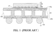
- FIG. 1 is a schematic cross-sectional view of a conventional flip-chip packaging structure.
- a bismaleimide-triazine (BT) packaging substrate 10 is provided.
- the packaging substrate 10 has a core layer 102 and opposite first and second surfaces 10a, 10b.
- a plurality of flip-chip bonding pads 100 are formed on the first surface 10a of the packaging substrate 10 and electrically connected to the electrode pads 120 of a semiconductor chip 12 through a plurality of solder bumps 11.
- An underfill 17 is filled between the first surface 10a of the packaging substrate 10 and the semiconductor chip 12 for encapsulating the solder bumps 11.
- solder ball bonding pads 101 are formed on the second surface 10b of the packaging substrate 10 such that solder balls 13can be mounted on the solder ball bonding pads 101 for electrically connecting an external electronic device such as a printed circuit board (not shown).
- the semiconductor chip 12 Since the semiconductor chip 12 is fabricated below 45nm node, a dielectric material having an extreme low k (ELK) or an ultra low k (ULK) is usually used in a back end of the line (BEOL) of the semiconductor chip 12.
- ELK extreme low k
- ULK ultra low k
- BEOL back end of the line
- such a low-k dielectric material is porous and brittle. Therefore, during a thermal cycling test for reliability characterization of the flip chip package, the solder bumps 11 can easily crack due to uneven thermal stresses caused by a big difference between the thermal expansion coefficients (CTEs) of the packaging substrate 10 and the semiconductor chip 12, thereby easily causing the semiconductor chip 12 to crack and hence reducing the product reliability.
- CTEs thermal expansion coefficients
- the semiconductor chip 12 tends to have a high density of nano-scale circuits and thus reduced pitches between the electrode pads 120.
- the flip-chip bonding pads 100 of the packaging substrate 10 are only of micro-scale pitches.
- the packaging substrate 10 is not suitable for the high-density nano-scale circuits of the semiconductor chip 12, thereby adversely affecting the fabrication of electronic products having reduced size and improved functions.
- the present invention provides a packaging substrate having an embedded interposer, which comprises: a carrier having opposite top and bottom surfaces, wherein a recess is disposed in the top surface of the carrier and a plurality of first conductive terminals are disposed on the bottom of the recess, and a plurality of second conductive terminals are disposed on the bottom surface of the carrier for electrically connecting the carrier and an external electronic device; and an interposer disposed in the recess and having opposite first and second surfaces and a plurality of conductive through vias penetrating the first and second surfaces, wherein a first conductive pad is disposed on an end of each of the conductive through vias exposed from the first surface so as for a semiconductor chip to be mounted and electrically connected thereto, and a second conductive pad is disposed on the other end of the conductive through via exposed from the second surface and is electrically connected to a corresponding one of the first conductive terminals.
- the present invention provides another packaging substrate having an embedded interposer, which comprises: a carrier having opposite top and bottom surfaces, wherein a recess is disposed in the top surface of the carrier and a plurality of first conductive terminals are disposed on the bottom of the recess, and a plurality of second conductive terminals are disposed on the bottom surface of the carrier for electrically connecting the carrier and an external electronic device; and an interposer disposed in the recess and having opposite first and second surfaces and a plurality of conductive through vias penetrating the first and second surfaces, wherein a first conductive pad is disposed on an end of each of the conductive through vias exposed from the first surface, and a second conductive pad is disposed on the other end of the conductive through via exposed from the second surface and electrically connected to a corresponding one of the first conductive terminals, further, a redistribution layer is disposed on the first surface and the first conductive pads, and the outermost redistribution layer has a plurality of extensive conductive pads
- the present invention further provides a fabrication method of a packaging substrate having an embedded interposer, which comprises the steps of: preparing a carrier having opposite top and bottom surfaces, wherein a recess is formed in the top surface of the carrier and a plurality of first conductive terminals are formed on the bottom of the recess, and a plurality of second conductive terminals are formed on the bottom surface of the carrier for electrically connecting the carrier and an external electronic device; and disposing in the recess an interposer having opposite first and second surfaces and a plurality of conductive through vias penetrating the first and second surfaces, wherein a first conductive pad is formed on an end of each of the conductive through vias exposed from the first surface, and a second conductive pad is formed on the other end of the conductive through via exposed from the second surface and electrically connected to a corresponding one of the first conductive terminals.
- the present invention provides a packaging substrate suitable for a semiconductor chip having high-density nano-scale circuits without changing original supply chains and infrastructures of IC industries. Further, since the CTEs of the interposer and the semiconductor chip are close to each other, the present invention prevents large thermal stresses from occurring between the semiconductor chip and the interposer, thereby effectively improving the product reliability. In addition, the present invention embeds the interposer in the packaging substrate so as to reduce the thickness of the overall structure.
- the present invention facilitates dissipation of heat generated by the packaging substrate and the semiconductor chip, thus avoiding damages of the packaging substrate that would otherwise occur due to large thermal stresses during a thermal cycling test or during the use of the product.
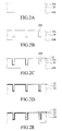
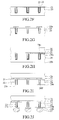
- FIGS.2A to 2L are schematic cross-sectional views showing a fabrication method of an interposer according to the present invention.
- a plate 20 having opposite first and second surfaces 20a, 20b is provided.
- the plate 20 can be made of silicon, poly-silicon or other semiconductor material.
- a plurality oftrenchs 200 are formed in the first surface 20a of the plate 20.
- a coater, an aligner and a developer can be used to form on the first surface 20a a photoresist layer (not shown) having a plurality of openings for exposing portions of the plate 20.
- the exposed portions of the plate 20 are etched by DRIE so as to form the trenchs 200.
- the photoresist layer is removed by such as a stripper.
- an insulating layer 21 made of such as silicon dioxide is formed on the first surface 20a and the surfaces of the trenchs 200 through plasma enhanced chemical vapor deposition (PECVD) or furnace process.
- PECVD plasma enhanced chemical vapor deposition
- a conductive layer 22 is formed on the insulating layer 21 through such as sputtering.
- a metal layer 23 made of such as copper is formed on the conductive layer 22 through electroplating.
- portions of the metal layer 23 and the conductive layer 22 higher than the top surface of the insulating layer 21 are removed by using such as a grinder, a polisher or through a chemical mechanical planarization (CMP) process.
- CMP chemical mechanical planarization
- a plurality of first conductive pads 24a are formed on the remaining portions of the metal layer 23 so as for a semiconductor chip to be mounted thereon.
- an under bump metallurgy (UBM) layer (not shown) can be formed on the first conductive pads 24a so as to improve the electrical connection reliability.
- a first carrier 26 is attached to the insulating layer 21 and the first conductive pads 24a through an adhesive layer 25.
- portions of the plate 20 and the insulating layer 21 are removed from the second surface 20b for exposing one ends 23a of the metal layer 23, thereby forming a plurality of conductive through vias penetrating the first surface 20a and the second surface 20b of the plate 20.
- Each of the conductive through vias has a through via 200' penetrating the first surface 20a and the second surface 20b, an insulating layer 21 formed on the sidewall of the through via 200' and a metal layer 23 filling the through via 200'.
- a plurality of second conductive pads 24b are formed on the exposed ends 23a of the metal layer 23, and a plurality of solder bumps 27 are further formed on the second conductive pads 24b.
- a UBM layer (not shown) can be first formed on the second conductive pads 24b and then the solder bumps 27 are formed on the UMB layer, thereby improving the electrical connection reliability
- a second carrier 28 is disposed on the second surface 20b for covering the solder bumps 27, and the first carrier 26 and the adhesive layer 25 are removed.
- the interposer does not have the insulating layer 21 and the conductive layer 22. That is, the metal layer 23 is directly formed to penetrate the plate 20.
- the plate 20 can be made of glass, ceramic such as Al 2 O 3 or AlN.
- the plate 20 is made of ceramic, since the coefficient of thermal expansion (CTE) of ceramic (approximately 3 ppm/ ⁇ ) is close to that of silicon.
- a cutting process is performed and the second carrier 28 is removed so as to obtain a plurality of interposers 2.
- a plurality of first conductive pads 24a' are formed on the metal layer 23 and further a redistribution layer (RDL) 29 is formed on the first surface 20a and the first conductive pads 24a'.
- the outermost redistribution layer 29 has a plurality of extensive conductive pads 291 so as for a semiconductor chip to be mounted and electrically connected thereto.
- a dielectric layer 61 can be formed on the second surface 20b.
- the dielectric layer 61 has a plurality of openings 610 for exposing the metal layer 23, and a plurality of second conductive pads 24b are formed in the openings 610, respectively.
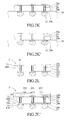
- FIGS.3A to 3G are schematic cross-sectional views showing a packaging substrate having an embedded interposer and a fabrication method thereof.
- a multi-layer interconnect base plate 30 is provided.
- the multi-layer interconnect base plate 30 has opposite third and fourth surfaces 30a, 30b and at least a circuit layer 301.
- the third surface 30a has a plurality of first conductive terminals 31a and a plurality of third conductive pads 32
- the fourth surface 30b has a plurality of second conductive terminals 31b.
- the circuit layer 301, the first conductive terminals 31a, the third conductive pads 32 and the second conductive terminals 31b can be made of copper.
- a UBM layer (not shown) can be formed on the first conductive terminals 31a and the second conductive terminals 31b for improving the electrical connection reliability.
- a built-up structure 33 is formed on the third surface 30a.
- the built-up structure 33 has a dielectric layer 331, a circuit layer 332 formed on the dielectric layer 331 and a plurality of conductive pads 332a exposed from the dielectric layer 331 and electrically connected to the circuit layer 332 and the third conductive pads 32.
- the dielectric layer 331 can be made of ABF (Ajinomoto Build-up Film) or BT (Bismaleimide-Triazine).
- the circuit layer 332 and the conductive pads 332a can be made of copper.
- portions of the dielectric layer 331 are removed through such as laser so as to form a cavity 330 exposing the first conductive terminals 31a.
- a first insulating protection layer 34a is formed on the built-up structure 33.
- the first insulating protection layer 34a has a plurality of first openings 340a exposing the conductive pads 332a, respectively.
- a second insulating protection layer 34b is formed on the fourth surface 30b and has a plurality of second openings 340b exposing the second conductive terminals 31b, respectively.
- the structure of FIG.3D can be simplified as or viewed as a carrier, which has a top surface (such as the top of the built-up structure 33) and a bottom surface (the fourth surface 30b of the multi-layer interconnect base plate 30) and a recess formed in the top surface.
- the bottom surface of the carrier has a plurality of conductive terminals for electrically connecting an external electronic device, and the bottom of the recess has a plurality of conductive terminals for electrically connecting the interposer 2.
- the interposer 2 of FIG.2L is disposed in the cavity 330 with the second conductive pads 24b electrically connected to the first conductive terminals 31a, respectively.
- a stress relief gap 330a is formed between the interposer 2 and the sidewall of the cavity 330.
- An underfill 35 is filled between the interposer 2 and the bottom of the cavity 330 so as to obtain a packaging substrate having an embedded interposer.
- a plurality of solder balls 36 can further be mounted on the second conductive terminals 31b.
- the interposer 2 of FIG.3F is replaced with the interposer 2 of FIG.2L' so as to obtain a structure of FIG. 3F' .
- a semiconductor chip 40 having an active surface 40a with a plurality of electrode pads 41 is disposed on the interposer 2.
- the electrode pads 41 of the active surface 40a are electrically connected to the first conductive pads 24a ( FIG. 3G-1 ), respectively, or electrically connected to the extensive conductive pads 291 ( FIG. 3G-1' ).
- the multi-layer interconnect base plate 30 of FIG. 3G-1 further has a metal pillar 51 penetrating the third and fourth surfaces 30a, 30b and connecting one of the first conductive terminals 31a.
- the multi-layer interconnect base plate 30 of FIG. 3G-1 further has a metal bump 52 disposed therein and connecting one of the first conductive terminals 31a.
- the multi-layer interconnect base plate 30 of FIG. 3G-3 further has a metal plate 53 disposed therein and connecting the bottom of the metal bump 52.
- the multi-layer interconnect base plate 30 of FIG. 3G-1 further has a metal bump 54 penetrating the third and fourth surfaces 30a, 30b and connecting one of the first conductive terminals 31a, and a metal plate 55 disposed on the fourth surface 30b and connecting the metal bump 54.
- the metal pillar 51, the metal bump 52, the metal plate 53, the metal bump 54 and the metal plate 55 are used to improve the heat dissipating effect so as to protect the packaging substrate from being damaged by overheating.
- the present invention further provides a packaging substrate having an embedded interposer, as shown in FIG.3F .
- the packaging substrate has a carrier and an interposer 2.
- the carrier has opposite top and bottom surfaces.
- a recess is disposed in the top surface of the carrier.
- a plurality of first conductive terminals 31a are disposed on the bottom of the recess, and a plurality of second conductive terminals 31b are disposed on the bottom surface of the carrier for electrically connecting the carrier and an external electronic device.
- the interposer 2 is disposed in the recess and has opposite first and second surfaces 20a, 20b, and a plurality of conductive through vias penetrating the first and second surfaces, 20a, 20b.
- a first conductive pad 24a is disposed on an end of each of the conductive through vias exposed from the first surface 20a so as for a semiconductor chip to be mounted and electrically connected thereto, and a second conductive pad 24b is disposed on the other end of the conductive through via exposed from the second surface 20b and is electrically connected to a corresponding one of the first conductive terminals 31a.
- the present invention provides another packaging substrate having an interposer.
- the packaging substrate has a carrier and an interposer 2.
- the carrier has opposite top and bottom surfaces.
- a recess is disposed in the top surface of the carrier and a plurality of first conductive terminals 31a are disposed on the bottom of the recess, and a plurality of second conductive terminals 31b are disposed on the bottom surface of the carrier for electrically connecting the carrier and an external electronic device.
- the interposer 2 is disposed in the recess and has opposite first and second surfaces 20a, 20b and a plurality of conductive through vias penetrating the first and second surfaces 20a, 20b.
- a first conductive pad 24a' is disposed on an end of each of the conductive through vias exposed from the first surface 20a
- a second conductive pad 24b is disposed on the other end of the conductive through via exposed from the second surface 20b and electrically connected to a corresponding one of the first conductive terminals 31a.
- a redistribution layer 29 is disposed on the first surface 20a and the first conductive pads 24a', and the outermost redistribution layer 29 has a plurality of extensive conductive pads 291 so as for a semiconductor chip to be mounted and electrically connected thereto.
- each of the conductive through vias can have a through via 200' penetrating the first surface 20a and the second surface 20b, an insulating layer 21 formed on the sidewall of the through via 200', and a metal layer 23 filling the through via 200'.
- the carrier can have a multi-layer interconnect base plate 20 and a built-up structure 33.
- the multi-layer interconnect base plate 20 has a third surface 20a and a fourth surface 30b opposite to the third surface 30a.
- the built-up structure 33 is formed on the third surface 30a and has a cavity 330 for exposing a portion of the multi-layer interconnect base plate 30.
- the packaging substrates can further have an underfill 35 formed between the interposer 2 and the bottom of the recess.
- the multi-layer interconnect base plate 30 can further have a metal pillar 51 penetrating the third and fourth surfaces 30a, 30b and connecting one of the first conductive terminals 31a.
- the multi-layer interconnect base plate 30 can further have a metal bump 52 disposed therein and connecting one of the first conductive terminals 31a.
- the multi-layer interconnect base plate 30 can further have a metal plate 53 disposed therein and connecting the bottom of the metal bump 52.
- the multi-layer interconnect base plate 30 can further have a metal bump 54 penetrating the third and fourth surfaces 30a, 30b and connecting one of the first conductive terminals 31a.
- the multi-layer interconnect base plate 30 can further have a metal plate 55 disposed therein and connecting the metal bump 54.
- a stress relief gap 330a can be disposed between the interposer 2 and the sidewall of the recess.
- the external electronic device can be a circuit board or other packaging structure.
- a coreless carrier is exemplified herein, it is not intended to limit the present invention.
- a carrier having a core can also be applied in the present invention.
- solder balls are used herein for electrically connecting the interposer and the carrier, the interposer and the semiconductor chip, and the carrier and the external electronic device, the present invention is not limited to the solder balls. Other electrical connection methods can be alternatively used.
- the present invention provides a packaging substrate suitable for a semiconductor chip having high-density nano-scale circuits without changing original supply chains and infrastructures of IC industries. Further, since the CTEs of the interposer and the semiconductor chip are close to each other, the present invention prevents large thermal stresses from occurring between the semiconductor chip and the interposer, thereby effectively improving the product reliability In addition, the present invention embeds the interposer in the packaging substrate so as to reduce the thickness of the overall structure.
- the present invention facilitates dissipation of heat generated by the packaging substrate and the semiconductor chip, thus avoiding damages of the packaging substrate that would otherwise occur due to large thermal stresses during a thermal cycling test or during the use of the product.
Landscapes
- Production Of Multi-Layered Print Wiring Board (AREA)
- Internal Circuitry In Semiconductor Integrated Circuit Devices (AREA)
Abstract
Description
- The present invention relates to packaging substrates and fabrication methods thereof, and more particularly, to a packaging substrate having an embedded interposer and a fabrication method thereof.
- Along with the rapid development of electronic industries, electronic products tend to have reduced size, high performance, multi-function and high speed.
FIG. 1 is a schematic cross-sectional view of a conventional flip-chip packaging structure. - Referring to
FIG.1 , a bismaleimide-triazine (BT)packaging substrate 10 is provided. Thepackaging substrate 10 has acore layer 102 and opposite first andsecond surfaces chip bonding pads 100 are formed on thefirst surface 10a of thepackaging substrate 10 and electrically connected to theelectrode pads 120 of asemiconductor chip 12 through a plurality ofsolder bumps 11. Anunderfill 17 is filled between thefirst surface 10a of thepackaging substrate 10 and thesemiconductor chip 12 for encapsulating thesolder bumps 11. Further, a plurality of solderball bonding pads 101 are formed on thesecond surface 10b of thepackaging substrate 10 such that solder balls 13can be mounted on the solderball bonding pads 101 for electrically connecting an external electronic device such as a printed circuit board (not shown). - Since the
semiconductor chip 12 is fabricated below 45nm node, a dielectric material having an extreme low k (ELK) or an ultra low k (ULK) is usually used in a back end of the line (BEOL) of thesemiconductor chip 12. However, such a low-k dielectric material is porous and brittle. Therefore, during a thermal cycling test for reliability characterization of the flip chip package, thesolder bumps 11 can easily crack due to uneven thermal stresses caused by a big difference between the thermal expansion coefficients (CTEs) of thepackaging substrate 10 and thesemiconductor chip 12, thereby easily causing thesemiconductor chip 12 to crack and hence reducing the product reliability. - Further, in order to obtain electronic products having reduced size and improved functions, the
semiconductor chip 12 tends to have a high density of nano-scale circuits and thus reduced pitches between theelectrode pads 120. On the other hand, the flip-chip bonding pads 100 of thepackaging substrate 10 are only of micro-scale pitches. Hence, thepackaging substrate 10 is not suitable for the high-density nano-scale circuits of thesemiconductor chip 12, thereby adversely affecting the fabrication of electronic products having reduced size and improved functions. - Therefore, there is a need to provide a packaging substrate and a fabrication method thereof so as to overcome the above-described drawbacks.
- Accordingly, the present invention provides a packaging substrate having an embedded interposer, which comprises: a carrier having opposite top and bottom surfaces, wherein a recess is disposed in the top surface of the carrier and a plurality of first conductive terminals are disposed on the bottom of the recess, and a plurality of second conductive terminals are disposed on the bottom surface of the carrier for electrically connecting the carrier and an external electronic device; and an interposer disposed in the recess and having opposite first and second surfaces and a plurality of conductive through vias penetrating the first and second surfaces, wherein a first conductive pad is disposed on an end of each of the conductive through vias exposed from the first surface so as for a semiconductor chip to be mounted and electrically connected thereto, and a second conductive pad is disposed on the other end of the conductive through via exposed from the second surface and is electrically connected to a corresponding one of the first conductive terminals.
- The present invention provides another packaging substrate having an embedded interposer, which comprises: a carrier having opposite top and bottom surfaces, wherein a recess is disposed in the top surface of the carrier and a plurality of first conductive terminals are disposed on the bottom of the recess, and a plurality of second conductive terminals are disposed on the bottom surface of the carrier for electrically connecting the carrier and an external electronic device; and an interposer disposed in the recess and having opposite first and second surfaces and a plurality of conductive through vias penetrating the first and second surfaces, wherein a first conductive pad is disposed on an end of each of the conductive through vias exposed from the first surface, and a second conductive pad is disposed on the other end of the conductive through via exposed from the second surface and electrically connected to a corresponding one of the first conductive terminals, further, a redistribution layer is disposed on the first surface and the first conductive pads, and the outermost redistribution layer has a plurality of extensive conductive pads so as for a semiconductor chip to be mounted and electrically connected thereto.
- The present invention further provides a fabrication method of a packaging substrate having an embedded interposer, which comprises the steps of: preparing a carrier having opposite top and bottom surfaces, wherein a recess is formed in the top surface of the carrier and a plurality of first conductive terminals are formed on the bottom of the recess, and a plurality of second conductive terminals are formed on the bottom surface of the carrier for electrically connecting the carrier and an external electronic device; and disposing in the recess an interposer having opposite first and second surfaces and a plurality of conductive through vias penetrating the first and second surfaces, wherein a first conductive pad is formed on an end of each of the conductive through vias exposed from the first surface, and a second conductive pad is formed on the other end of the conductive through via exposed from the second surface and electrically connected to a corresponding one of the first conductive terminals.
- Therefore, by providing the interposer, the present invention provides a packaging substrate suitable for a semiconductor chip having high-density nano-scale circuits without changing original supply chains and infrastructures of IC industries. Further, since the CTEs of the interposer and the semiconductor chip are close to each other, the present invention prevents large thermal stresses from occurring between the semiconductor chip and the interposer, thereby effectively improving the product reliability. In addition, the present invention embeds the interposer in the packaging substrate so as to reduce the thickness of the overall structure. Furthermore, by embedding a metal post, a metal bump or a metal plate in the packaging substrate, the present invention facilitates dissipation of heat generated by the packaging substrate and the semiconductor chip, thus avoiding damages of the packaging substrate that would otherwise occur due to large thermal stresses during a thermal cycling test or during the use of the product.
-
-
FIG.1 is a schematic cross-sectional view showing a conventional flip-chip packaging structure; -
FIGS.2A to 2L are schematic cross-sectional views showing a fabrication method of an interposer according to the present invention, whereinFIGS.2K' and 2L' show other embodiments ofFIGS.2K and 2L , respectively; and -
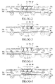
FIGS.3A to 3G are schematic cross-sectional views showing a fabrication method of a packaging substrate having an embedded interposer according to the present invention, whereinFIG. 3F' shows another embodiment ofFIG.3F , andFIGS. 3G-1', 3G-2, 3G-3, 3G-4 and 3G-5 show other embodiments ofFIG. 3G-1 . - The following illustrative embodiments are provided to illustrate the disclosure of the present invention, these and other advantages and effects can be apparent to those in the art after reading this specification.
- It should be noted that all the drawings are not intended to limit the present invention. Various modification and variations can be made without departing from the spirit of the present invention. Further, terms such as "one", "on", "top", "bottom" etc. are merely for illustrative purpose and should not be construed to limit the scope of the present invention.
- Generally, the implementation of the present invention is divided into two stages: firstly, an interposer is prepared; and secondly, a packaging substrate having an embedded interposer is fabricated.
FIGS.2A to 2L are schematic cross-sectional views showing a fabrication method of an interposer according to the present invention. - Referring to
FIG.2A , aplate 20 having opposite first andsecond surfaces plate 20 can be made of silicon, poly-silicon or other semiconductor material. - Referring to
FIG.2B , a plurality oftrenchs 200 are formed in thefirst surface 20a of theplate 20. To form thetrenchs 200, a coater, an aligner and a developer can be used to form on thefirst surface 20a a photoresist layer (not shown) having a plurality of openings for exposing portions of theplate 20. Then, the exposed portions of theplate 20 are etched by DRIE so as to form thetrenchs 200. Finally, the photoresist layer is removed by such as a stripper. - Referring to
FIG.2C , aninsulating layer 21 made of such as silicon dioxide is formed on thefirst surface 20a and the surfaces of thetrenchs 200 through plasma enhanced chemical vapor deposition (PECVD) or furnace process. - Referring to
FIG.2D , aconductive layer 22 is formed on theinsulating layer 21 through such as sputtering. - Referring to
FIG.2E , ametal layer 23 made of such as copper is formed on theconductive layer 22 through electroplating. - Referring to
FIG.2F , portions of themetal layer 23 and theconductive layer 22 higher than the top surface of theinsulating layer 21 are removed by using such as a grinder, a polisher or through a chemical mechanical planarization (CMP) process. - Referring to
FIG.2G , a plurality of firstconductive pads 24a are formed on the remaining portions of themetal layer 23 so as for a semiconductor chip to be mounted thereon. According to the practical need, an under bump metallurgy (UBM) layer (not shown) can be formed on the firstconductive pads 24a so as to improve the electrical connection reliability. - Referring to
FIG.2H , afirst carrier 26 is attached to theinsulating layer 21 and the firstconductive pads 24a through anadhesive layer 25. - Referring to
FIG.2I , portions of theplate 20 and theinsulating layer 21 are removed from thesecond surface 20b for exposing oneends 23a of themetal layer 23, thereby forming a plurality of conductive through vias penetrating thefirst surface 20a and thesecond surface 20b of theplate 20. Each of the conductive through vias has a through via 200' penetrating thefirst surface 20a and thesecond surface 20b, aninsulating layer 21 formed on the sidewall of the through via 200' and ametal layer 23 filling the through via 200'. - Referring to
FIG.2J , a plurality of secondconductive pads 24b are formed on the exposedends 23a of themetal layer 23, and a plurality ofsolder bumps 27 are further formed on the secondconductive pads 24b. According to the practical need, a UBM layer (not shown) can be first formed on the secondconductive pads 24b and then thesolder bumps 27 are formed on the UMB layer, thereby improving the electrical connection reliability - Referring to
FIG.2K , asecond carrier 28 is disposed on thesecond surface 20b for covering thesolder bumps 27, and thefirst carrier 26 and theadhesive layer 25 are removed. - In another embodiment, referring to
FIG. 2K' , the interposer does not have theinsulating layer 21 and theconductive layer 22. That is, themetal layer 23 is directly formed to penetrate theplate 20. Therein, theplate 20 can be made of glass, ceramic such as Al2O3 or AlN. Preferably, theplate 20 is made of ceramic, since the coefficient of thermal expansion (CTE) of ceramic (approximately 3 ppm/□) is close to that of silicon. - Referring to
FIG.2L , a cutting process is performed and thesecond carrier 28 is removed so as to obtain a plurality ofinterposers 2. - In another embodiment, referring to
FIG. 2L' , a plurality of firstconductive pads 24a' are formed on themetal layer 23 and further a redistribution layer (RDL) 29 is formed on thefirst surface 20a and the firstconductive pads 24a'. Theoutermost redistribution layer 29 has a plurality of extensiveconductive pads 291 so as for a semiconductor chip to be mounted and electrically connected thereto. Moreover, adielectric layer 61 can be formed on thesecond surface 20b. Thedielectric layer 61 has a plurality ofopenings 610 for exposing themetal layer 23, and a plurality of secondconductive pads 24b are formed in theopenings 610, respectively. -
FIGS.3A to 3G are schematic cross-sectional views showing a packaging substrate having an embedded interposer and a fabrication method thereof. - Referring to
FIG.3A , a multi-layerinterconnect base plate 30 is provided. The multi-layerinterconnect base plate 30 has opposite third andfourth surfaces circuit layer 301. Thethird surface 30a has a plurality of firstconductive terminals 31a and a plurality of thirdconductive pads 32, and thefourth surface 30b has a plurality of secondconductive terminals 31b. Thecircuit layer 301, the firstconductive terminals 31a, the thirdconductive pads 32 and the secondconductive terminals 31b can be made of copper. According to the practical need, a UBM layer (not shown) can be formed on the firstconductive terminals 31a and the secondconductive terminals 31b for improving the electrical connection reliability. - Referring to
FIG.3B , a built-upstructure 33 is formed on thethird surface 30a. The built-upstructure 33 has adielectric layer 331, acircuit layer 332 formed on thedielectric layer 331 and a plurality ofconductive pads 332a exposed from thedielectric layer 331 and electrically connected to thecircuit layer 332 and the thirdconductive pads 32. Thedielectric layer 331 can be made of ABF (Ajinomoto Build-up Film) or BT (Bismaleimide-Triazine). Thecircuit layer 332 and theconductive pads 332a can be made of copper. - Referring to
FIG.3C , portions of thedielectric layer 331 are removed through such as laser so as to form acavity 330 exposing the firstconductive terminals 31a. - Referring to
FIG.3D , a first insulatingprotection layer 34a is formed on the built-upstructure 33. The first insulatingprotection layer 34a has a plurality offirst openings 340a exposing theconductive pads 332a, respectively. A second insulatingprotection layer 34b is formed on thefourth surface 30b and has a plurality ofsecond openings 340b exposing the secondconductive terminals 31b, respectively. - In another embodiment, the structure of
FIG.3D can be simplified as or viewed as a carrier, which has a top surface (such as the top of the built-up structure 33) and a bottom surface (thefourth surface 30b of the multi-layer interconnect base plate 30) and a recess formed in the top surface. The bottom surface of the carrier has a plurality of conductive terminals for electrically connecting an external electronic device, and the bottom of the recess has a plurality of conductive terminals for electrically connecting theinterposer 2. - Referring to
FIG.3E , theinterposer 2 ofFIG.2L is disposed in thecavity 330 with the secondconductive pads 24b electrically connected to the firstconductive terminals 31a, respectively. Astress relief gap 330a is formed between theinterposer 2 and the sidewall of thecavity 330. Anunderfill 35 is filled between theinterposer 2 and the bottom of thecavity 330 so as to obtain a packaging substrate having an embedded interposer. - Referring to
FIG.3F , a plurality ofsolder balls 36 can further be mounted on the secondconductive terminals 31b. Alternatively, theinterposer 2 ofFIG.3F is replaced with theinterposer 2 ofFIG.2L' so as to obtain a structure ofFIG. 3F' . - Referring to
FIGS. 3G-1 and 3G-1' that are continued fromFIGS. 3F and 3F' , respectively, asemiconductor chip 40 having anactive surface 40a with a plurality ofelectrode pads 41 is disposed on theinterposer 2. Theelectrode pads 41 of theactive surface 40a are electrically connected to the firstconductive pads 24a (FIG. 3G-1 ), respectively, or electrically connected to the extensive conductive pads 291 (FIG. 3G-1' ). - Referring to
FIG. 3G-2 , the multi-layerinterconnect base plate 30 ofFIG. 3G-1 further has ametal pillar 51 penetrating the third andfourth surfaces conductive terminals 31a. - Referring to
FIG. 3G-3 , the multi-layerinterconnect base plate 30 ofFIG. 3G-1 further has ametal bump 52 disposed therein and connecting one of the firstconductive terminals 31a. - Referring to
FIG. 3G-4 , the multi-layerinterconnect base plate 30 ofFIG. 3G-3 further has ametal plate 53 disposed therein and connecting the bottom of themetal bump 52. - Referring to
FIG. 3G-5 , the multi-layerinterconnect base plate 30 ofFIG. 3G-1 further has ametal bump 54 penetrating the third andfourth surfaces conductive terminals 31a, and ametal plate 55 disposed on thefourth surface 30b and connecting themetal bump 54. - It should be noted that the
metal pillar 51, themetal bump 52, themetal plate 53, themetal bump 54 and themetal plate 55 are used to improve the heat dissipating effect so as to protect the packaging substrate from being damaged by overheating. - The present invention further provides a packaging substrate having an embedded interposer, as shown in
FIG.3F . The packaging substrate has a carrier and aninterposer 2. The carrier has opposite top and bottom surfaces. A recess is disposed in the top surface of the carrier. A plurality of firstconductive terminals 31a are disposed on the bottom of the recess, and a plurality of secondconductive terminals 31b are disposed on the bottom surface of the carrier for electrically connecting the carrier and an external electronic device. Theinterposer 2 is disposed in the recess and has opposite first andsecond surfaces conductive pad 24a is disposed on an end of each of the conductive through vias exposed from thefirst surface 20a so as for a semiconductor chip to be mounted and electrically connected thereto, and a secondconductive pad 24b is disposed on the other end of the conductive through via exposed from thesecond surface 20b and is electrically connected to a corresponding one of the firstconductive terminals 31a. - The present invention provides another packaging substrate having an interposer. Referring to
FIG. 3F' , the packaging substrate has a carrier and aninterposer 2. The carrier has opposite top and bottom surfaces. A recess is disposed in the top surface of the carrier and a plurality of firstconductive terminals 31a are disposed on the bottom of the recess, and a plurality of secondconductive terminals 31b are disposed on the bottom surface of the carrier for electrically connecting the carrier and an external electronic device. Theinterposer 2 is disposed in the recess and has opposite first andsecond surfaces second surfaces conductive pad 24a' is disposed on an end of each of the conductive through vias exposed from thefirst surface 20a, and a secondconductive pad 24b is disposed on the other end of the conductive through via exposed from thesecond surface 20b and electrically connected to a corresponding one of the firstconductive terminals 31a. Further, aredistribution layer 29 is disposed on thefirst surface 20a and the firstconductive pads 24a', and theoutermost redistribution layer 29 has a plurality of extensiveconductive pads 291 so as for a semiconductor chip to be mounted and electrically connected thereto. - In the above-describe packaging substrates, each of the conductive through vias can have a through via 200' penetrating the
first surface 20a and thesecond surface 20b, an insulatinglayer 21 formed on the sidewall of the through via 200', and ametal layer 23 filling the through via 200'. - In the above-described packaging substrates, the carrier can have a multi-layer
interconnect base plate 20 and a built-upstructure 33. The multi-layerinterconnect base plate 20 has athird surface 20a and afourth surface 30b opposite to thethird surface 30a. The built-upstructure 33 is formed on thethird surface 30a and has acavity 330 for exposing a portion of the multi-layerinterconnect base plate 30. - The packaging substrates can further have an
underfill 35 formed between theinterposer 2 and the bottom of the recess. - In the above-described packaging substrates, the multi-layer
interconnect base plate 30 can further have ametal pillar 51 penetrating the third andfourth surfaces conductive terminals 31a. - The multi-layer
interconnect base plate 30 can further have ametal bump 52 disposed therein and connecting one of the firstconductive terminals 31a. The multi-layerinterconnect base plate 30 can further have ametal plate 53 disposed therein and connecting the bottom of themetal bump 52. - The multi-layer
interconnect base plate 30 can further have ametal bump 54 penetrating the third andfourth surfaces conductive terminals 31a. The multi-layerinterconnect base plate 30 can further have ametal plate 55 disposed therein and connecting themetal bump 54. - A
stress relief gap 330a can be disposed between theinterposer 2 and the sidewall of the recess. - It should be noted that the external electronic device can be a circuit board or other packaging structure. Although a coreless carrier is exemplified herein, it is not intended to limit the present invention. A carrier having a core can also be applied in the present invention. In addition, although solder balls are used herein for electrically connecting the interposer and the carrier, the interposer and the semiconductor chip, and the carrier and the external electronic device, the present invention is not limited to the solder balls. Other electrical connection methods can be alternatively used.
- Therefore, by providing the interposer, the present invention provides a packaging substrate suitable for a semiconductor chip having high-density nano-scale circuits without changing original supply chains and infrastructures of IC industries. Further, since the CTEs of the interposer and the semiconductor chip are close to each other, the present invention prevents large thermal stresses from occurring between the semiconductor chip and the interposer, thereby effectively improving the product reliability In addition, the present invention embeds the interposer in the packaging substrate so as to reduce the thickness of the overall structure. Furthermore, by embedding a metal post, a metal bump or a metal plate in the packaging substrate, the present invention facilitates dissipation of heat generated by the packaging substrate and the semiconductor chip, thus avoiding damages of the packaging substrate that would otherwise occur due to large thermal stresses during a thermal cycling test or during the use of the product.
- The above-described descriptions of the detailed embodiments are only to illustrate the preferred implementation according to the present invention, and it is not to limit the scope of the present invention. Accordingly, all modifications and variations completed by those with ordinary skill in the art should fall within the scope of present invention defined by the appended claims.
Claims (12)
- A packaging substrate having an embedded interposer, comprising:a carrier having opposite top and bottom surfaces, wherein a recess is formed on the top surface of the carrier and a plurality of first conductive terminals are formed in the recess, and a plurality of second conductive terminals are disposed on the bottom surface of the carrier for electrically connecting the carrier and an external electronic device; andan interposer disposed in the recess and having opposite first and second surfaces and a plurality of conductive through vias penetrating the first and second surfaces, wherein a first conductive pad is formed on an end of each of the conductive through vias exposed from the first surface so as for a semiconductor chip to be mounted thereon and electrically connected thereto, and a second conductive pad is formed on the other end of each of the conductive through vias exposed from the second surface and is electrically connected to a corresponding one of the first conductive terminals.
- A packaging substrate having an embedded interposer, comprising:a carrier having opposite top and bottom surfaces, wherein a recess is formed on the top surface of the carrier and a plurality of first conductive terminals are formed in the recess, and a plurality of second conductive terminals are formed on the bottom surface of the carrier for electrically connecting the carrier and an external electronic device; andan interposer disposed in the recess and having opposite first and second surfaces and a plurality of conductive through vias penetrating the first and second surfaces, wherein a first conductive pad is disposed on an end of each of the conductive through vias exposed from the first surface, a second conductive pad is formed on the other end of each of the conductive through vias exposed from the second surface and electrically connected to a corresponding one of the first conductive terminals, and a redistribution layer is formed on the first surface and the first conductive pads, and the outermost sub-layer of the redistribution layer has a plurality of extensive conductive pads so as for a semiconductor chip to be mounted thereon and electrically connected thereto.
- The substrate of claim 1 or claim 2, wherein each of the conductive through vias has a through hole penetrating the first and second surfaces, an insulating layer formed on a sidewall of the through hole and a metal layer filling the through hole.
- The substrate of claim 1 or claim 2, wherein the carrier comprises: a multi-layer interconnect base plate having opposite third and fourth surfaces, and a built-up structure formed on the third surface of the multi-layer interconnect base plate and having a cavity for exposing a portion of the multi-layer interconnect base plate.
- The substrate of claim 1 or claim 2, wherein the multi-layer interconnect base plate further has at least a metal pillar penetrating the third and fourth surfaces and electrically connecting at least one of the first conductive terminals.
- The substrate of claim 1 or claim 2, wherein the multi-layer interconnect base plate further has at least a metal bump disposed therein and electrically connecting at least one of the first conductive terminals.
- The substrate of claim 1 or claim 2, wherein the multi-layer interconnect base plate further has at least a metal plate disposed therein and electrically connecting the bottom surface of the metal bump.
- The substrate of claim 4, wherein the multi-layer interconnect base plate further has at least a metal bump penetrating the third and fourth surfaces and electrically connecting at least one of the first conductive terminals, and a metal plate disposed on the fourth surface and electrically connecting the at least a metal bump.
- The substrate of claim 1 or claim 2, wherein a stress relief gap is formed between the interposer and the recess.
- A fabrication method of a packaging substrate having an embedded interposer, comprising the steps of:preparing a carrier having opposite top and bottom surfaces, wherein a recess is formed on the top surface of the carrier and a plurality of first conductive terminals are formed on the recess, and a plurality of second conductive terminals are formed on the bottom surface of the carrier for electrically connecting the carrier and an external electronic device; anddisposing in the recess an interposer having opposite first and second surfaces and a plurality of conductive through vias penetrating the first and second surfaces, wherein a first conductive pad is formed on an end of each of the conductive through vias exposed from the first surface, and a second conductive pad is formed on the other end of each of the conductive through vias exposed from the second surface and electrically connected to a corresponding one of the first conductive terminals.
- The method of claim 10, further comprising forming a redistribution layer on the first surface of the interposer and the first conductive pads, wherein the outermost sub-layer of the redistribution layer has a plurality of extensive conductive pads so as for a semiconductor chip to be mounted thereon and electrically connected thereto.
- The method of claim 10, wherein the fabrication of the carrier comprises:preparing a multi-layer interconnect base plate having opposite third and fourth surfaces;forming a built-up structure on the third surface of the multi-layer interconnect base plate; andremoving a portion of the built-up structure so as to form a cavity for exposing a portion of the multi-layer interconnect base plate.
Applications Claiming Priority (1)
| Application Number | Priority Date | Filing Date | Title |
|---|---|---|---|
| TW100128085A TWI492680B (en) | 2011-08-05 | 2011-08-05 | Package substrate with interposer embedded therein and method of making same |
Publications (2)
| Publication Number | Publication Date |
|---|---|
| EP2555240A1 true EP2555240A1 (en) | 2013-02-06 |
| EP2555240B1 EP2555240B1 (en) | 2020-04-15 |
Family
ID=46727109
Family Applications (1)
| Application Number | Title | Priority Date | Filing Date |
|---|---|---|---|
| EP12179424.2A Active EP2555240B1 (en) | 2011-08-05 | 2012-08-06 | Packaging substrate having embedded interposer and fabrication method thereof |
Country Status (5)
| Country | Link |
|---|---|
| US (1) | US9385056B2 (en) |
| EP (1) | EP2555240B1 (en) |
| JP (1) | JP5396508B2 (en) |
| CN (1) | CN102915983B (en) |
| TW (1) | TWI492680B (en) |
Cited By (6)
| Publication number | Priority date | Publication date | Assignee | Title |
|---|---|---|---|---|
| WO2014152756A1 (en) * | 2013-03-14 | 2014-09-25 | Invensas Corporation | Low cte interposer without tsv structure and method |
| EP2978020A1 (en) * | 2014-07-25 | 2016-01-27 | Dyi-Chung Hu | Package substrate |
| US10181447B2 (en) | 2017-04-21 | 2019-01-15 | Invensas Corporation | 3D-interconnect |
| US10748840B2 (en) | 2008-05-09 | 2020-08-18 | Invensas Corporation | Chip-size, double side connection package and method for manufacturing the same |
| US12040284B2 (en) | 2021-11-12 | 2024-07-16 | Invensas Llc | 3D-interconnect with electromagnetic interference (“EMI”) shield and/or antenna |
| EP4415041A4 (en) * | 2022-12-20 | 2024-09-25 | Chengdu Haiguang Integrated Circuit Design Co., Ltd. | ELECTRONIC HOUSING, MANUFACTURING METHOD FOR ELECTRONIC HOUSING AND ELECTRONIC DEVICE |
Families Citing this family (79)
| Publication number | Priority date | Publication date | Assignee | Title |
|---|---|---|---|---|
| US10026720B2 (en) * | 2015-05-20 | 2018-07-17 | Broadpak Corporation | Semiconductor structure and a method of making thereof |
| US9679836B2 (en) * | 2011-11-16 | 2017-06-13 | Taiwan Semiconductor Manufacturing Company, Ltd. | Package structures and methods for forming the same |
| US9282646B2 (en) * | 2012-05-24 | 2016-03-08 | Unimicron Technology Corp. | Interposed substrate and manufacturing method thereof |
| US9330943B2 (en) * | 2012-12-12 | 2016-05-03 | Apple Inc. | Low cost repackaging of thinned integrated devices |
| US9257355B2 (en) * | 2013-02-11 | 2016-02-09 | The Charles Stark Draper Laboratory, Inc. | Method for embedding a chipset having an intermediary interposer in high density electronic modules |
| CN104218016A (en) * | 2013-06-04 | 2014-12-17 | 宏启胜精密电子(秦皇岛)有限公司 | IC carrier board and semiconductor device with the IC carrier board |
| KR101538539B1 (en) * | 2013-06-20 | 2015-07-21 | 앰코 테크놀로지 코리아 주식회사 | Semiconductor device and manufacturing method thereof |
| CN104377187B (en) * | 2013-08-16 | 2017-06-23 | 碁鼎科技秦皇岛有限公司 | IC support plates, the semiconductor devices with the IC support plates and preparation method |
| CN104425286A (en) * | 2013-08-23 | 2015-03-18 | 宏启胜精密电子(秦皇岛)有限公司 | IC carrier plate, semiconductor device having the same and manufacturing method of the IC carrier plate |
| CN104427747B (en) * | 2013-08-30 | 2017-10-10 | 深南电路有限公司 | A kind of internal layer buries the circuit board and its processing method of copper |
| TWI515829B (en) * | 2013-08-30 | 2016-01-01 | 南茂科技股份有限公司 | Wafer level packaging method and package structure |
| CN104576596B (en) * | 2013-10-25 | 2019-01-01 | 日月光半导体制造股份有限公司 | Semiconductor substrate and method for manufacturing the same |
| US10199321B2 (en) * | 2015-09-03 | 2019-02-05 | Bridge Semiconductor Corporation | Interconnect substrate having cavity for stackable semiconductor assembly, manufacturing method thereof and vertically stacked semiconductor assembly using the same |
| US9355997B2 (en) | 2014-03-12 | 2016-05-31 | Invensas Corporation | Integrated circuit assemblies with reinforcement frames, and methods of manufacture |
| US20150262902A1 (en) | 2014-03-12 | 2015-09-17 | Invensas Corporation | Integrated circuits protected by substrates with cavities, and methods of manufacture |
| TWI549201B (en) * | 2014-04-08 | 2016-09-11 | 矽品精密工業股份有限公司 | Package structure and its manufacturing method |
| US9165793B1 (en) | 2014-05-02 | 2015-10-20 | Invensas Corporation | Making electrical components in handle wafers of integrated circuit packages |
| US9741649B2 (en) | 2014-06-04 | 2017-08-22 | Invensas Corporation | Integrated interposer solutions for 2D and 3D IC packaging |
| US9252127B1 (en) | 2014-07-10 | 2016-02-02 | Invensas Corporation | Microelectronic assemblies with integrated circuits and interposers with cavities, and methods of manufacture |
| TWI660476B (en) * | 2014-07-11 | 2019-05-21 | Siliconware Precision Industries Co., Ltd. | Package structure and method of manufacture |
| JP2016082163A (en) * | 2014-10-21 | 2016-05-16 | イビデン株式会社 | Printed wiring board |
| TWI557853B (en) * | 2014-11-12 | 2016-11-11 | 矽品精密工業股份有限公司 | Semiconductor package and its manufacturing method |
| US20160204056A1 (en) * | 2015-01-14 | 2016-07-14 | Bridge Semiconductor Corporation | Wiring board with interposer and dual wiring structures integrated together and method of making the same |
| US9859159B2 (en) * | 2015-03-10 | 2018-01-02 | Unimicron Technology Corp. | Interconnection structure and manufacturing method thereof |
| CN106033753B (en) * | 2015-03-12 | 2019-07-12 | 恒劲科技股份有限公司 | Packaging module and substrate structure thereof |
| US9478504B1 (en) | 2015-06-19 | 2016-10-25 | Invensas Corporation | Microelectronic assemblies with cavities, and methods of fabrication |
| CN107750388A (en) * | 2015-06-25 | 2018-03-02 | 英特尔公司 | Integrated circuit structure with interposer with groove |
| US10651102B2 (en) | 2015-12-18 | 2020-05-12 | Intel IP Corporation | Interposer with conductive routing exposed on sidewalls |
| EP3437129A4 (en) * | 2016-03-30 | 2019-09-25 | INTEL Corporation | Hybrid microelectronic substrates |
| US9806061B2 (en) * | 2016-03-31 | 2017-10-31 | Altera Corporation | Bumpless wafer level fan-out package |
| KR102019352B1 (en) | 2016-06-20 | 2019-09-09 | 삼성전자주식회사 | Fan-out semiconductor package |
| US9761535B1 (en) * | 2016-06-27 | 2017-09-12 | Nanya Technology Corporation | Interposer, semiconductor package with the same and method for preparing a semiconductor package with the same |
| US11355427B2 (en) * | 2016-07-01 | 2022-06-07 | Intel Corporation | Device, method and system for providing recessed interconnect structures of a substrate |
| US20180020547A1 (en) * | 2016-07-13 | 2018-01-18 | Alcatel-Lucent Canada Inc. | Underlying recessed component placement |
| TWI643275B (en) * | 2016-08-29 | 2018-12-01 | 上海兆芯集成電路有限公司 | Electronic structure process |
| TWI647805B (en) * | 2016-09-09 | 2019-01-11 | 矽品精密工業股份有限公司 | Electronic package and its manufacturing method |
| KR102591624B1 (en) * | 2016-10-31 | 2023-10-20 | 삼성전자주식회사 | Semiconductor packages |
| TWI669797B (en) * | 2016-11-16 | 2019-08-21 | 矽品精密工業股份有限公司 | Substrate electronic device and method of manufacturing electronic device |
| US20180240778A1 (en) * | 2017-02-22 | 2018-08-23 | Intel Corporation | Embedded multi-die interconnect bridge with improved power delivery |
| US10217720B2 (en) | 2017-06-15 | 2019-02-26 | Invensas Corporation | Multi-chip modules formed using wafer-level processing of a reconstitute wafer |
| US10373893B2 (en) | 2017-06-30 | 2019-08-06 | Intel Corporation | Embedded bridge with through-silicon vias |
| CN107393900B (en) * | 2017-08-08 | 2019-07-26 | 中国电子科技集团公司第五十八研究所 | The embedded type TSV adapter plate structure of pole multilayer wiring |
| KR101942742B1 (en) * | 2017-10-26 | 2019-01-28 | 삼성전기 주식회사 | Fan-out semiconductor package |
| CN110071073B (en) * | 2018-01-22 | 2022-03-22 | 江苏长电科技股份有限公司 | Package structure and preparation method thereof |
| CN110246812A (en) * | 2018-03-08 | 2019-09-17 | 恒劲科技股份有限公司 | A kind of semiconductor package and preparation method thereof |
| US20190287872A1 (en) * | 2018-03-19 | 2019-09-19 | Intel Corporation | Multi-use package architecture |
| TWI714296B (en) * | 2019-10-04 | 2020-12-21 | 欣興電子股份有限公司 | Package substrate and manufacturing method thereof |
| US11373927B2 (en) | 2018-05-30 | 2022-06-28 | Unimicron Technology Corp. | Package substrate and manufacturing method having a mesh gas-permeable structure disposed in the through hole |
| US20200020624A1 (en) * | 2018-07-10 | 2020-01-16 | Qualcomm Incorporated | Substrate-embedded substrate |
| TWI662676B (en) * | 2018-08-31 | 2019-06-11 | 欣興電子股份有限公司 | Circuit carrier with embedded substrate, manufacturing method thereof and chip package structure |
| CN109244058A (en) * | 2018-09-19 | 2019-01-18 | 深圳铨力半导体有限公司 | Semiconductor package and preparation method thereof |
| KR102568705B1 (en) | 2018-10-05 | 2023-08-22 | 삼성전자주식회사 | Semiconductor package, method for semiconductor package and method for re-distribution layer structure |
| KR102540829B1 (en) | 2018-10-05 | 2023-06-08 | 삼성전자주식회사 | Semiconductor package, method for semiconductor package and method for re-distribution layer structure |
| US11049779B2 (en) * | 2018-10-12 | 2021-06-29 | Dyi-chung Hu | Carrier for chip packaging and manufacturing method thereof |
| KR102574410B1 (en) * | 2018-11-27 | 2023-09-04 | 삼성전기주식회사 | Hybrid interposer and semiconductor package including the same |
| IT201900006740A1 (en) * | 2019-05-10 | 2020-11-10 | Applied Materials Inc | SUBSTRATE STRUCTURING PROCEDURES |
| IT201900006736A1 (en) | 2019-05-10 | 2020-11-10 | Applied Materials Inc | PACKAGE MANUFACTURING PROCEDURES |
| US11289401B2 (en) * | 2019-05-15 | 2022-03-29 | Powertech Technology Inc. | Semiconductor package |
| CN110310895B (en) * | 2019-07-31 | 2024-06-21 | 中国电子科技集团公司第五十八研究所 | A method and structure for embedding TSV transfer chip silicon-based fan-out three-dimensional integrated packaging |
| TWI735034B (en) * | 2019-08-27 | 2021-08-01 | 鈺橋半導體股份有限公司 | Interconnect substrate with stiffener and warp balancer and semiconductor assembly using the same |
| CN110491853B (en) * | 2019-09-16 | 2024-08-09 | 中国电子科技集团公司第五十八研究所 | A silicon-based three-dimensional fan-out integrated packaging method and structure |
| CN112635432A (en) * | 2019-10-09 | 2021-04-09 | 欣兴电子股份有限公司 | Package substrate and manufacturing method thereof |
| US11527462B2 (en) | 2019-12-13 | 2022-12-13 | International Business Machines Corporation | Circuit substrate with mixed pitch wiring |
| US11948877B2 (en) * | 2020-03-31 | 2024-04-02 | Qualcomm Incorporated | Hybrid package apparatus and method of fabricating |
| TWI758756B (en) * | 2020-06-23 | 2022-03-21 | 欣興電子股份有限公司 | Package carrier and manufacturing method thereof |
| KR102915100B1 (en) | 2020-12-14 | 2026-01-21 | 삼성전자주식회사 | Semiconductor package |
| TWI820402B (en) * | 2021-03-08 | 2023-11-01 | 欣興電子股份有限公司 | Wiring board with embedded interposer substrate and method of fabricating the same |
| CN115052435A (en) * | 2021-03-08 | 2022-09-13 | 欣兴电子股份有限公司 | Circuit board embedded with intermediate substrate and forming method thereof |
| TWI777741B (en) * | 2021-08-23 | 2022-09-11 | 欣興電子股份有限公司 | Substrate with buried component and manufacture method thereof |
| US12051632B2 (en) * | 2021-08-30 | 2024-07-30 | Taiwan Semiconductor Manufacturing Company, Ltd. | Semiconductor package structure and method for forming semiconductor package structure |
| CN118302858A (en) * | 2021-09-01 | 2024-07-05 | 美商艾德亚半导体科技有限责任公司 | Stacked structure with interposer |
| CN116013874A (en) | 2021-10-22 | 2023-04-25 | 讯芯电子科技(中山)有限公司 | Semiconductor package device and semiconductor package device manufacturing method |
| US20230282588A1 (en) * | 2022-03-02 | 2023-09-07 | Micron Technology, Inc. | Semiconductor assemblies with systems and methods for using an interchangeable interposer to connect die to common substrate |
| CN114725056B (en) * | 2022-03-11 | 2025-11-25 | 艾司博国际有限公司 | Embedded fan-out package structure and its manufacturing method |
| CN114743945B (en) * | 2022-03-11 | 2025-11-25 | 艾司博国际有限公司 | Advanced Packaging Structures with Si and Organic Intermediate Layers and Their Manufacturing Methods |
| US20240096779A1 (en) * | 2022-09-20 | 2024-03-21 | Advanced Semiconductor Engineering, Inc. | Flexible package |
| CN115881654B (en) * | 2023-01-31 | 2023-08-22 | 深圳新声半导体有限公司 | Packaging structure of embedded filter and radio frequency front end module and preparation method thereof |
| US12571959B2 (en) * | 2023-04-03 | 2026-03-10 | Intel Corporation | Embedded photonic integrated circuits |
| CN120341202A (en) * | 2025-04-15 | 2025-07-18 | 芯爱科技(南京)有限公司 | Auxiliary fixture and its manufacturing method and application |
Citations (2)
| Publication number | Priority date | Publication date | Assignee | Title |
|---|---|---|---|---|
| US20090073667A1 (en) * | 2007-09-18 | 2009-03-19 | Samsung Electro-Mechanics Co., Ltd. | Semiconductor chip package and printed circuit board |
| US20100081236A1 (en) * | 2008-10-01 | 2010-04-01 | Samsung Electronics Co., Ltd | Method of manufacturing semiconductor device with embedded interposer |
Family Cites Families (14)
| Publication number | Priority date | Publication date | Assignee | Title |
|---|---|---|---|---|
| CN1094717C (en) * | 1995-11-16 | 2002-11-20 | 松下电器产业株式会社 | PC board and fixing body thereof |
| JP3635219B2 (en) * | 1999-03-11 | 2005-04-06 | 新光電気工業株式会社 | Multilayer substrate for semiconductor device and manufacturing method thereof |
| US6529022B2 (en) * | 2000-12-15 | 2003-03-04 | Eaglestone Pareners I, Llc | Wafer testing interposer for a conventional package |
| JP3849573B2 (en) * | 2001-05-22 | 2006-11-22 | 株式会社日立製作所 | Electronic equipment |
| US6800930B2 (en) * | 2002-07-31 | 2004-10-05 | Micron Technology, Inc. | Semiconductor dice having back side redistribution layer accessed using through-silicon vias, and assemblies |
| JP2004296627A (en) * | 2003-03-26 | 2004-10-21 | Renesas Technology Corp | Semiconductor device |
| JP2006019441A (en) * | 2004-06-30 | 2006-01-19 | Shinko Electric Ind Co Ltd | Manufacturing method of electronic component built-in substrate |
| US7462784B2 (en) * | 2006-05-02 | 2008-12-09 | Ibiden Co., Ltd. | Heat resistant substrate incorporated circuit wiring board |
| US20080017407A1 (en) * | 2006-07-24 | 2008-01-24 | Ibiden Co., Ltd. | Interposer and electronic device using the same |
| JP2008218942A (en) * | 2007-03-08 | 2008-09-18 | Matsushita Electric Ind Co Ltd | Electronic circuit device, electronic apparatus using the same, and manufacturing method thereof |
| JP5306634B2 (en) * | 2007-11-22 | 2013-10-02 | 新光電気工業株式会社 | WIRING BOARD, SEMICONDUCTOR DEVICE, AND WIRING BOARD MANUFACTURING METHOD |
| JP5079475B2 (en) * | 2007-12-05 | 2012-11-21 | 新光電気工業株式会社 | Electronic component mounting package |
| JP5577760B2 (en) * | 2009-03-09 | 2014-08-27 | 新光電気工業株式会社 | Package substrate and method for manufacturing semiconductor device |
| JP4906903B2 (en) * | 2009-10-20 | 2012-03-28 | 新光電気工業株式会社 | Manufacturing method of electronic component built-in substrate |
-
2011
- 2011-08-05 TW TW100128085A patent/TWI492680B/en active
-
2012
- 2012-05-16 JP JP2012112371A patent/JP5396508B2/en active Active
- 2012-07-30 CN CN201210266187.0A patent/CN102915983B/en active Active
- 2012-08-03 US US13/566,323 patent/US9385056B2/en active Active
- 2012-08-06 EP EP12179424.2A patent/EP2555240B1/en active Active
Patent Citations (2)
| Publication number | Priority date | Publication date | Assignee | Title |
|---|---|---|---|---|
| US20090073667A1 (en) * | 2007-09-18 | 2009-03-19 | Samsung Electro-Mechanics Co., Ltd. | Semiconductor chip package and printed circuit board |
| US20100081236A1 (en) * | 2008-10-01 | 2010-04-01 | Samsung Electronics Co., Ltd | Method of manufacturing semiconductor device with embedded interposer |
Cited By (14)
| Publication number | Priority date | Publication date | Assignee | Title |
|---|---|---|---|---|
| US10748840B2 (en) | 2008-05-09 | 2020-08-18 | Invensas Corporation | Chip-size, double side connection package and method for manufacturing the same |
| WO2014152756A1 (en) * | 2013-03-14 | 2014-09-25 | Invensas Corporation | Low cte interposer without tsv structure and method |
| US8884427B2 (en) | 2013-03-14 | 2014-11-11 | Invensas Corporation | Low CTE interposer without TSV structure |
| US9558964B2 (en) | 2013-03-14 | 2017-01-31 | Invensas Corporation | Method of fabricating low CTE interposer without TSV structure |
| US10396114B2 (en) | 2013-03-14 | 2019-08-27 | Invensas Corporation | Method of fabricating low CTE interposer without TSV structure |
| US10373918B2 (en) | 2014-07-25 | 2019-08-06 | Dyi-chung Hu | Package substrate |
| US9627285B2 (en) | 2014-07-25 | 2017-04-18 | Dyi-chung Hu | Package substrate |
| EP2978020A1 (en) * | 2014-07-25 | 2016-01-27 | Dyi-Chung Hu | Package substrate |
| US10181447B2 (en) | 2017-04-21 | 2019-01-15 | Invensas Corporation | 3D-interconnect |
| US11031362B2 (en) | 2017-04-21 | 2021-06-08 | Invensas Corporation | 3D-interconnect |
| US11929337B2 (en) | 2017-04-21 | 2024-03-12 | Invensas Llc | 3D-interconnect |
| US12476212B2 (en) | 2017-04-21 | 2025-11-18 | Adeia Semiconductor Technologies Llc | 3D-interconnect |
| US12040284B2 (en) | 2021-11-12 | 2024-07-16 | Invensas Llc | 3D-interconnect with electromagnetic interference (“EMI”) shield and/or antenna |
| EP4415041A4 (en) * | 2022-12-20 | 2024-09-25 | Chengdu Haiguang Integrated Circuit Design Co., Ltd. | ELECTRONIC HOUSING, MANUFACTURING METHOD FOR ELECTRONIC HOUSING AND ELECTRONIC DEVICE |
Also Published As
| Publication number | Publication date |
|---|---|
| US20130032390A1 (en) | 2013-02-07 |
| CN102915983B (en) | 2015-10-28 |
| US9385056B2 (en) | 2016-07-05 |
| JP5396508B2 (en) | 2014-01-22 |
| EP2555240B1 (en) | 2020-04-15 |
| CN102915983A (en) | 2013-02-06 |
| JP2013038386A (en) | 2013-02-21 |
| TW201309123A (en) | 2013-02-16 |
| TWI492680B (en) | 2015-07-11 |
Similar Documents
| Publication | Publication Date | Title |
|---|---|---|
| US9385056B2 (en) | Packaging substrate having embedded interposer and fabrication method thereof | |
| US8946564B2 (en) | Packaging substrate having embedded through-via interposer and method of fabricating the same | |
| US11387171B2 (en) | Method of packaging a semiconductor die | |
| US8269337B2 (en) | Packaging substrate having through-holed interposer embedded therein and fabrication method thereof | |
| US9502335B2 (en) | Package structure and method for fabricating the same | |
| KR101366461B1 (en) | Semiconductor device and manufacturing method thereof | |
| US10096541B2 (en) | Method for fabricating electronic package | |
| TWI399843B (en) | Semiconductor device and method of manufacturing same | |
| US10049973B2 (en) | Electronic package and fabrication method thereof and substrate structure | |
| TW201813018A (en) | Fan-out wafer level package type semiconductor package and stacked package type semiconductor package including the same | |
| US20140117538A1 (en) | Package structure and fabrication method thereof | |
| US9875949B2 (en) | Electronic package having circuit structure with plurality of metal layers, and fabrication method thereof | |
| CN106653703A (en) | Package-on-package structure | |
| CN102376667A (en) | Packaging device and manufacturing method thereof | |
| CN108074905B (en) | Electronic device and its manufacturing method and substrate structure | |
| CN101335224B (en) | Semiconductor package structure and manufacturing method thereof | |
| US8603911B2 (en) | Semiconductor device and fabrication method thereof | |
| US20160050753A1 (en) | Interposer and fabrication method thereof |
Legal Events
| Date | Code | Title | Description |
|---|---|---|---|
| PUAI | Public reference made under article 153(3) epc to a published international application that has entered the european phase |
Free format text: ORIGINAL CODE: 0009012 |
|
| AK | Designated contracting states |
Kind code of ref document: A1 Designated state(s): AL AT BE BG CH CY CZ DE DK EE ES FI FR GB GR HR HU IE IS IT LI LT LU LV MC MK MT NL NO PL PT RO RS SE SI SK SM TR |
|
| AX | Request for extension of the european patent |
Extension state: BA ME |
|
| 17P | Request for examination filed |
Effective date: 20130806 |
|
| RBV | Designated contracting states (corrected) |
Designated state(s): AL AT BE BG CH CY CZ DE DK EE ES FI FR GB GR HR HU IE IS IT LI LT LU LV MC MK MT NL NO PL PT RO RS SE SI SK SM TR |
|
| STAA | Information on the status of an ep patent application or granted ep patent |
Free format text: STATUS: EXAMINATION IS IN PROGRESS |
|
| 17Q | First examination report despatched |
Effective date: 20180918 |
|
| REG | Reference to a national code |
Ref country code: DE Ref legal event code: R079 Ref document number: 602012069262 Country of ref document: DE Free format text: PREVIOUS MAIN CLASS: H01L0025065000 Ipc: H01L0023140000 |
|
| RIC1 | Information provided on ipc code assigned before grant |
Ipc: H01L 23/13 20060101ALI20190912BHEP Ipc: H01L 23/14 20060101AFI20190912BHEP Ipc: H01L 23/498 20060101ALI20190912BHEP |
|
| GRAP | Despatch of communication of intention to grant a patent |
Free format text: ORIGINAL CODE: EPIDOSNIGR1 |
|
| STAA | Information on the status of an ep patent application or granted ep patent |
Free format text: STATUS: GRANT OF PATENT IS INTENDED |
|
| INTG | Intention to grant announced |
Effective date: 20191120 |
|
| RAP1 | Party data changed (applicant data changed or rights of an application transferred) |
Owner name: UNIMICRON TECHNOLOGY CORP. Owner name: INDUSTRIAL TECHNOLOGY RESEARCH INSTITUTE |
|
| GRAS | Grant fee paid |
Free format text: ORIGINAL CODE: EPIDOSNIGR3 |
|
| GRAA | (expected) grant |
Free format text: ORIGINAL CODE: 0009210 |
|
| STAA | Information on the status of an ep patent application or granted ep patent |
Free format text: STATUS: THE PATENT HAS BEEN GRANTED |
|
| AK | Designated contracting states |
Kind code of ref document: B1 Designated state(s): AL AT BE BG CH CY CZ DE DK EE ES FI FR GB GR HR HU IE IS IT LI LT LU LV MC MK MT NL NO PL PT RO RS SE SI SK SM TR |
|
| REG | Reference to a national code |
Ref country code: CH Ref legal event code: EP Ref country code: GB Ref legal event code: FG4D |
|
| REG | Reference to a national code |
Ref country code: DE Ref legal event code: R096 Ref document number: 602012069262 Country of ref document: DE |
|
| REG | Reference to a national code |
Ref country code: IE Ref legal event code: FG4D |
|
| REG | Reference to a national code |
Ref country code: AT Ref legal event code: REF Ref document number: 1258289 Country of ref document: AT Kind code of ref document: T Effective date: 20200515 |
|
| REG | Reference to a national code |
Ref country code: NL Ref legal event code: MP Effective date: 20200415 |
|
| REG | Reference to a national code |
Ref country code: LT Ref legal event code: MG4D |
|
| PG25 | Lapsed in a contracting state [announced via postgrant information from national office to epo] |
Ref country code: FI Free format text: LAPSE BECAUSE OF FAILURE TO SUBMIT A TRANSLATION OF THE DESCRIPTION OR TO PAY THE FEE WITHIN THE PRESCRIBED TIME-LIMIT Effective date: 20200415 Ref country code: GR Free format text: LAPSE BECAUSE OF FAILURE TO SUBMIT A TRANSLATION OF THE DESCRIPTION OR TO PAY THE FEE WITHIN THE PRESCRIBED TIME-LIMIT Effective date: 20200716 Ref country code: NO Free format text: LAPSE BECAUSE OF FAILURE TO SUBMIT A TRANSLATION OF THE DESCRIPTION OR TO PAY THE FEE WITHIN THE PRESCRIBED TIME-LIMIT Effective date: 20200715 Ref country code: IS Free format text: LAPSE BECAUSE OF FAILURE TO SUBMIT A TRANSLATION OF THE DESCRIPTION OR TO PAY THE FEE WITHIN THE PRESCRIBED TIME-LIMIT Effective date: 20200815 Ref country code: PT Free format text: LAPSE BECAUSE OF FAILURE TO SUBMIT A TRANSLATION OF THE DESCRIPTION OR TO PAY THE FEE WITHIN THE PRESCRIBED TIME-LIMIT Effective date: 20200817 Ref country code: LT Free format text: LAPSE BECAUSE OF FAILURE TO SUBMIT A TRANSLATION OF THE DESCRIPTION OR TO PAY THE FEE WITHIN THE PRESCRIBED TIME-LIMIT Effective date: 20200415 Ref country code: NL Free format text: LAPSE BECAUSE OF FAILURE TO SUBMIT A TRANSLATION OF THE DESCRIPTION OR TO PAY THE FEE WITHIN THE PRESCRIBED TIME-LIMIT Effective date: 20200415 Ref country code: SE Free format text: LAPSE BECAUSE OF FAILURE TO SUBMIT A TRANSLATION OF THE DESCRIPTION OR TO PAY THE FEE WITHIN THE PRESCRIBED TIME-LIMIT Effective date: 20200415 |
|
| REG | Reference to a national code |
Ref country code: AT Ref legal event code: MK05 Ref document number: 1258289 Country of ref document: AT Kind code of ref document: T Effective date: 20200415 |
|
| PG25 | Lapsed in a contracting state [announced via postgrant information from national office to epo] |
Ref country code: HR Free format text: LAPSE BECAUSE OF FAILURE TO SUBMIT A TRANSLATION OF THE DESCRIPTION OR TO PAY THE FEE WITHIN THE PRESCRIBED TIME-LIMIT Effective date: 20200415 Ref country code: LV Free format text: LAPSE BECAUSE OF FAILURE TO SUBMIT A TRANSLATION OF THE DESCRIPTION OR TO PAY THE FEE WITHIN THE PRESCRIBED TIME-LIMIT Effective date: 20200415 Ref country code: RS Free format text: LAPSE BECAUSE OF FAILURE TO SUBMIT A TRANSLATION OF THE DESCRIPTION OR TO PAY THE FEE WITHIN THE PRESCRIBED TIME-LIMIT Effective date: 20200415 Ref country code: BG Free format text: LAPSE BECAUSE OF FAILURE TO SUBMIT A TRANSLATION OF THE DESCRIPTION OR TO PAY THE FEE WITHIN THE PRESCRIBED TIME-LIMIT Effective date: 20200715 |
|
| PG25 | Lapsed in a contracting state [announced via postgrant information from national office to epo] |
Ref country code: AL Free format text: LAPSE BECAUSE OF FAILURE TO SUBMIT A TRANSLATION OF THE DESCRIPTION OR TO PAY THE FEE WITHIN THE PRESCRIBED TIME-LIMIT Effective date: 20200415 |
|
| REG | Reference to a national code |
Ref country code: DE Ref legal event code: R097 Ref document number: 602012069262 Country of ref document: DE |
|
| PG25 | Lapsed in a contracting state [announced via postgrant information from national office to epo] |
Ref country code: ES Free format text: LAPSE BECAUSE OF FAILURE TO SUBMIT A TRANSLATION OF THE DESCRIPTION OR TO PAY THE FEE WITHIN THE PRESCRIBED TIME-LIMIT Effective date: 20200415 Ref country code: CZ Free format text: LAPSE BECAUSE OF FAILURE TO SUBMIT A TRANSLATION OF THE DESCRIPTION OR TO PAY THE FEE WITHIN THE PRESCRIBED TIME-LIMIT Effective date: 20200415 Ref country code: RO Free format text: LAPSE BECAUSE OF FAILURE TO SUBMIT A TRANSLATION OF THE DESCRIPTION OR TO PAY THE FEE WITHIN THE PRESCRIBED TIME-LIMIT Effective date: 20200415 Ref country code: EE Free format text: LAPSE BECAUSE OF FAILURE TO SUBMIT A TRANSLATION OF THE DESCRIPTION OR TO PAY THE FEE WITHIN THE PRESCRIBED TIME-LIMIT Effective date: 20200415 Ref country code: DK Free format text: LAPSE BECAUSE OF FAILURE TO SUBMIT A TRANSLATION OF THE DESCRIPTION OR TO PAY THE FEE WITHIN THE PRESCRIBED TIME-LIMIT Effective date: 20200415 Ref country code: AT Free format text: LAPSE BECAUSE OF FAILURE TO SUBMIT A TRANSLATION OF THE DESCRIPTION OR TO PAY THE FEE WITHIN THE PRESCRIBED TIME-LIMIT Effective date: 20200415 Ref country code: IT Free format text: LAPSE BECAUSE OF FAILURE TO SUBMIT A TRANSLATION OF THE DESCRIPTION OR TO PAY THE FEE WITHIN THE PRESCRIBED TIME-LIMIT Effective date: 20200415 Ref country code: SM Free format text: LAPSE BECAUSE OF FAILURE TO SUBMIT A TRANSLATION OF THE DESCRIPTION OR TO PAY THE FEE WITHIN THE PRESCRIBED TIME-LIMIT Effective date: 20200415 |
|
| PLBE | No opposition filed within time limit |
Free format text: ORIGINAL CODE: 0009261 |
|
| STAA | Information on the status of an ep patent application or granted ep patent |
Free format text: STATUS: NO OPPOSITION FILED WITHIN TIME LIMIT |
|
| PG25 | Lapsed in a contracting state [announced via postgrant information from national office to epo] |
Ref country code: SK Free format text: LAPSE BECAUSE OF FAILURE TO SUBMIT A TRANSLATION OF THE DESCRIPTION OR TO PAY THE FEE WITHIN THE PRESCRIBED TIME-LIMIT Effective date: 20200415 Ref country code: PL Free format text: LAPSE BECAUSE OF FAILURE TO SUBMIT A TRANSLATION OF THE DESCRIPTION OR TO PAY THE FEE WITHIN THE PRESCRIBED TIME-LIMIT Effective date: 20200415 |
|
| 26N | No opposition filed |
Effective date: 20210118 |
|
| PG25 | Lapsed in a contracting state [announced via postgrant information from national office to epo] |
Ref country code: MC Free format text: LAPSE BECAUSE OF FAILURE TO SUBMIT A TRANSLATION OF THE DESCRIPTION OR TO PAY THE FEE WITHIN THE PRESCRIBED TIME-LIMIT Effective date: 20200415 |
|
| REG | Reference to a national code |
Ref country code: CH Ref legal event code: PL |
|
| GBPC | Gb: european patent ceased through non-payment of renewal fee |
Effective date: 20200806 |
|
| PG25 | Lapsed in a contracting state [announced via postgrant information from national office to epo] |
Ref country code: LU Free format text: LAPSE BECAUSE OF NON-PAYMENT OF DUE FEES Effective date: 20200806 Ref country code: LI Free format text: LAPSE BECAUSE OF NON-PAYMENT OF DUE FEES Effective date: 20200831 Ref country code: CH Free format text: LAPSE BECAUSE OF NON-PAYMENT OF DUE FEES Effective date: 20200831 |
|
| REG | Reference to a national code |
Ref country code: BE Ref legal event code: MM Effective date: 20200831 |
|
| PG25 | Lapsed in a contracting state [announced via postgrant information from national office to epo] |
Ref country code: SI Free format text: LAPSE BECAUSE OF FAILURE TO SUBMIT A TRANSLATION OF THE DESCRIPTION OR TO PAY THE FEE WITHIN THE PRESCRIBED TIME-LIMIT Effective date: 20200415 |
|
| PG25 | Lapsed in a contracting state [announced via postgrant information from national office to epo] |
Ref country code: BE Free format text: LAPSE BECAUSE OF NON-PAYMENT OF DUE FEES Effective date: 20200831 Ref country code: GB Free format text: LAPSE BECAUSE OF NON-PAYMENT OF DUE FEES Effective date: 20200806 Ref country code: IE Free format text: LAPSE BECAUSE OF NON-PAYMENT OF DUE FEES Effective date: 20200806 |
|
| PG25 | Lapsed in a contracting state [announced via postgrant information from national office to epo] |
Ref country code: TR Free format text: LAPSE BECAUSE OF FAILURE TO SUBMIT A TRANSLATION OF THE DESCRIPTION OR TO PAY THE FEE WITHIN THE PRESCRIBED TIME-LIMIT Effective date: 20200415 Ref country code: MT Free format text: LAPSE BECAUSE OF FAILURE TO SUBMIT A TRANSLATION OF THE DESCRIPTION OR TO PAY THE FEE WITHIN THE PRESCRIBED TIME-LIMIT Effective date: 20200415 Ref country code: CY Free format text: LAPSE BECAUSE OF FAILURE TO SUBMIT A TRANSLATION OF THE DESCRIPTION OR TO PAY THE FEE WITHIN THE PRESCRIBED TIME-LIMIT Effective date: 20200415 |
|
| PG25 | Lapsed in a contracting state [announced via postgrant information from national office to epo] |
Ref country code: MK Free format text: LAPSE BECAUSE OF FAILURE TO SUBMIT A TRANSLATION OF THE DESCRIPTION OR TO PAY THE FEE WITHIN THE PRESCRIBED TIME-LIMIT Effective date: 20200415 |
|
| PGFP | Annual fee paid to national office [announced via postgrant information from national office to epo] |
Ref country code: FR Payment date: 20250610 Year of fee payment: 14 |
|
| PGFP | Annual fee paid to national office [announced via postgrant information from national office to epo] |
Ref country code: DE Payment date: 20250611 Year of fee payment: 14 |
|
| REG | Reference to a national code |
Ref country code: DE Ref legal event code: R079 Ref document number: 602012069262 Country of ref document: DE Free format text: PREVIOUS MAIN CLASS: H01L0023140000 Ipc: H10W0070690000 |