EP2550671B1 - Lithography system, sensor, converter element and method of manufacture - Google Patents
Lithography system, sensor, converter element and method of manufacture Download PDFInfo
- Publication number
- EP2550671B1 EP2550671B1 EP11709423.5A EP11709423A EP2550671B1 EP 2550671 B1 EP2550671 B1 EP 2550671B1 EP 11709423 A EP11709423 A EP 11709423A EP 2550671 B1 EP2550671 B1 EP 2550671B1
- Authority
- EP
- European Patent Office
- Prior art keywords
- layer
- converter element
- charged particle
- beamlets
- sensor
- Prior art date
- Legal status (The legal status is an assumption and is not a legal conclusion. Google has not performed a legal analysis and makes no representation as to the accuracy of the status listed.)
- Active
Links
Images

Classifications
-
- H—ELECTRICITY
- H01—ELECTRIC ELEMENTS
- H01J—ELECTRIC DISCHARGE TUBES OR DISCHARGE LAMPS
- H01J37/00—Discharge tubes with provision for introducing objects or material to be exposed to the discharge, e.g. for the purpose of examination or processing thereof
- H01J37/02—Details
- H01J37/244—Detectors; Associated components or circuits therefor
-
- B—PERFORMING OPERATIONS; TRANSPORTING
- B82—NANOTECHNOLOGY
- B82Y—SPECIFIC USES OR APPLICATIONS OF NANOSTRUCTURES; MEASUREMENT OR ANALYSIS OF NANOSTRUCTURES; MANUFACTURE OR TREATMENT OF NANOSTRUCTURES
- B82Y10/00—Nanotechnology for information processing, storage or transmission, e.g. quantum computing or single electron logic
-
- B—PERFORMING OPERATIONS; TRANSPORTING
- B82—NANOTECHNOLOGY
- B82Y—SPECIFIC USES OR APPLICATIONS OF NANOSTRUCTURES; MEASUREMENT OR ANALYSIS OF NANOSTRUCTURES; MANUFACTURE OR TREATMENT OF NANOSTRUCTURES
- B82Y40/00—Manufacture or treatment of nanostructures
-
- H—ELECTRICITY
- H01—ELECTRIC ELEMENTS
- H01J—ELECTRIC DISCHARGE TUBES OR DISCHARGE LAMPS
- H01J37/00—Discharge tubes with provision for introducing objects or material to be exposed to the discharge, e.g. for the purpose of examination or processing thereof
- H01J37/30—Electron-beam or ion-beam tubes for localised treatment of objects
- H01J37/304—Controlling tubes by information coming from the objects or from the beam, e.g. correction signals
- H01J37/3045—Object or beam position registration
-
- H—ELECTRICITY
- H01—ELECTRIC ELEMENTS
- H01J—ELECTRIC DISCHARGE TUBES OR DISCHARGE LAMPS
- H01J37/00—Discharge tubes with provision for introducing objects or material to be exposed to the discharge, e.g. for the purpose of examination or processing thereof
- H01J37/30—Electron-beam or ion-beam tubes for localised treatment of objects
- H01J37/317—Electron-beam or ion-beam tubes for localised treatment of objects for changing properties of the objects or for applying thin layers thereon, e.g. for ion implantation
- H01J37/3174—Particle-beam lithography, e.g. electron beam lithography
- H01J37/3177—Multi-beam, e.g. fly's eye, comb probe
-
- H—ELECTRICITY
- H01—ELECTRIC ELEMENTS
- H01J—ELECTRIC DISCHARGE TUBES OR DISCHARGE LAMPS
- H01J2237/00—Discharge tubes exposing object to beam, e.g. for analysis treatment, etching, imaging
- H01J2237/244—Detection characterized by the detecting means
- H01J2237/2443—Scintillation detectors
Definitions
- the present invention relates to a charged particle lithography system, in particular to a maskless charged particle system, to a sensor therefore, in particular for determining charged particle beam properties, to a converter element therefore, as well as to a method of manufacturing the same.
- Charged-particle beamlet lithography systems make use of a plurality of charged particle beamlets to transfer a pattern onto the surface of a target.
- the beamlets may write the pattern by being scanned over the target surface while their trajectory may be controllably blocked so as to create a beamlet that can be turned on or off.
- Blocking may be established by electrostatic deflection of beamlets on a blocking surface.
- the size and shape of the beamlets may be adapted along the trajectory. Deflection, shaping and/or size adaptation may be executed by one or more electron optical components like for example an aperture array, an array of electrostatic deflectors and/or beamlet blankers.
- Such lithography systems can have very large numbers of beamlets, i.e. in the order of 10,000 or higher, for example 13,000. Future designs even envisage numbers in the order of 1,000,000 beamlets. It is a general aim for current electron beam lithography systems to be able to pattern a target surface in high-resolution, with some applications being capable of imaging patterns with a critical dimension of well below 100 nm feature sizes.
- Deviating beamlets may severely affect the quality of the pattern to be written. It is therefore desirable to detect these deviations so that corrective measures may be taken.
- each beamlet In conventional lithography systems, the position of each beamlet is determined by frequent measurement of the beamlet position. With knowledge of the beamlet position the beamlet can be shifted to the correct position. For accurate writing it is beneficial to determine the beamlet position within a distance in the order of a few nanometres.
- Known beamlet position calibration methods generally comprise at least three steps: a measuring step in which the position of the beamlet is measured, a calculating step in which the measured position of the beamlet is compared to the desired expected position of that beamlet, and a compensation step in which the difference between the measured position and the desired position is compensated for. Compensation may be performed either in the software or in the hardware of the lithography system.
- Desired specifications for spot size measurements include determination of beamlet spot sizes in the range of 30 nm to 150 nm; accuracy of spot size measurements with 3 sigma value smaller than 5 nm; and a reproducibility of such spot size measurements within a single sensor with 3 sigma value smaller than 5 nm.
- a sensor for measuring properties of a large number of charged-particle beamlets, in particular for charged particle beamlets used in a lithography system, is described in US published patent application 2007/057204 .
- US 2007/057204 describes a sensor and method in which charged-particle beamlets are converted into light beams, using a converter element such as a fluorescent screen or a doped YAG material. Subsequently, the light beams are detected by an array of light sensitive detectors such as diodes, CCD or CMOS devices. A relatively fast measurement can be achieved by reading out a large number of light sensitive detectors in a single operation. Additionally the sensor structure, in particular the array of light detectors, enables a very small pitch of a multiplicity of beams to be measured without the necessity of unduly large structural measures in the region of the stage part of a lithography system.
- the present invention provides a charged particle beamlet lithography system for transferring a pattern to a surface of a target comprising a sensor for determining one or more characteristics of one or more charged particle beamlets, the sensor comprising a converter element for receiving charged particles and generating photons in response, the converter element comprising a surface for receiving one or more charged particle beamlets, the surface being provided with one or more cells for evaluating one or more individual beamlets, each cell comprising a predetermined blocking pattern of one or more charged particle blocking structures forming multiple knife edges at transitions between blocking and non-blocking regions along a predetermined beamlet scan trajectory over the converter element surface, wherein the converter element surface is covered with a coating layer substantially permeable for the charged particles and substantially impermeable for ambient light, and wherein the sensor further comprises an electrically conductive layer between the coating layer and the blocking structures.
- the coating layer allows the sensor to respond in a more uniform manner to the receipt of charged particles over a considerable area of the converter element surface, for example over an area of about 3 x 3 mm 2 .
- the coating layer removes local influences from ambient light, for example background radiation or the like. As a result, a plurality of beamlets may be sensed simultaneously with high resolution.
- Suitable materials for use in the coating layer include titanium (Ti) and aluminum (Al).
- the blocking structures generally comprise a heavy metal like tungsten (W), and providing such structures on top of a substrate generally includes one or more etching steps.
- the material being used for the electrically conductive layer preferably has a high selectivity for such etching steps.
- a suitable material that may be included in the material forming the electrically conductive layer is chromium (Cr).
- Cr chromium
- the invention relates to a method of manufacturing a converter element for selectively converting impinging charged particles into photons.
- the method comprises: providing a substrate comprising a conversion material for converting charged particles into photons; subsequently coating the substrate with a first layer comprising an electrically conductive material, a second layer comprising an etch stop material and a third layer comprising a third material; providing a resist layer on top of said third layer; patterning, and developing the resist layer so as to form a first predetermined pattern, and etching the developed resist layer until the third layer is exposed; coating the exposed third layer with a fourth layer comprising a further etch stop material; lifting of the developed resist such that the third layer is exposed in accordance with a second predetermined pattern, the second predetermined pattern being an inversion of the first predetermined pattern; etching the third layer in accordance with the second predetermined pattern until the second layer is exposed; etching the fourth layer as well as the second layer in accordance with the second predetermined pattern until the first layer is exposed.
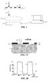
- FIG. 1 schematically shows the operation of a sensor for determining one or more characteristics of particle beams, in particular one or more characteristics of charged particle beamlets.
- the sensor comprises a converter element 1 and a photon receptor 5.
- the converter element is provided with a pattern comprising charged particle blocking regions 8 and charged particle transmissive regions 7, further referred to as non-blocking regions.
- the converter element 1 is arranged for receiving charged particles 2 and generating photons 3 in response.
- the photons 3 may be directed towards the photon receptor 5 by means of an optical system 11.
- the photon receptor 5 is communicatively coupled to a calculation unit, e.g. a computer 13 for determining one or more characteristics of the charged particles 2.
- the converter element 1 may take the form of a fluorescent element, for example a fluorescent screen, or a scintillating element, for example a substrate of a doped yttrium aluminum garnet (YAG) material.
- YAG yttrium aluminum garnet
- the photon receptor 5 may include any suitable light sensitive detector, such as a plurality of diodes, charged coupled device (CCD) cameras or complementary metal-oxide semiconductor (CMOS) cameras.
- CCD charged coupled device
- CMOS complementary metal-oxide semiconductor
- the photon receptor 5 may be referred to as camera 5.
- embodiments of the invention may be used for any type of (charged) particles or light beams 2, hereafter, embodiments of the invention will be discussed with reference to electrons.
- FIG. 2A schematically shows a cross-section of a YAG 1 comprising an electron beamlet receiving surface provided with an electron blocking structure.
- the electron blocking structure comprises electron blocking regions provided with a layer 18 capable of blocking electrons.
- the blocking layer 18 may be a metal layer.
- a suitable metal for blocking electrons is tungsten. In between the blocking regions are non-blocking regions.
- An electron beam 22 impinging onto a non-blocking region of the electron blocking structure actually impinges onto the surface of the YAG 1 or a coating on the surface of the YAG.
- the additional layer 21 serves the purpose of increasing the uniformity of the blocking layer 18.
- the additional layer 21 may be a metal layer.
- An example of a particularly suitable material for use in the additional layer 21 is chromium.
- the YAG 1 is coated with a coating layer 20.
- the coating layer 20 may be a metal layer for blocking background radiation.
- the coating layer 20 is substantially permeable to charged particles on the one hand, while being substantially impermeable for ambient light on the other hand. For this reason, the thickness of the coating layer 20 is sufficient to establish both functions.
- Suitable materials for the coating layer 20 include aluminum and titanium.
- the electron beam 22 may be scanned over a blocking structure provided on the YAG 1 (in FIG. 2A in a direction denoted as X-direction).
- photons generated within the YAG 1 may be detected by a camera.
- An exemplary result of such scanning and detection action is schematically depicted in FIG. 2B .
- FIG. 2B shows a graph representing intensity of light emitted by a converter element 1 as a function of x-position of an electron beam 22 over the surface of the converter element 1.
- a maximum response is observed when electron beam 22 is entirely positioned in a non-blocking region, and minimal light is generated if the electron beam 22 is positioned entirely on top of a blocking region. The crossing of a knife edge results in a steep change of light intensity.
- intensity levels exceeding a higher threshold value T h are provided as high level signal values to a processor.
- detected intensity levels below a lower threshold value T l may be provided as low level signal values.
- the use of threshold values T h , T l may enable the use of digital processing.
- the electron beamlet may encounter two types of situations while crossing a knife edge. In a first situation, the beamlet experiences a transition from a blocking region to a non-blocking region. In a second situation, the beamlet experiences a transition from a non-blocking region to a blocking region.
- Knife edges being encountered during a transition that corresponds to the first situation may be referred to as knife edges of a first type.
- knife edges being encountered during a transition that corresponds to the second situation may be referred to as knife edges of a second type.
- the type of knife edge is thus dependent on the scanning direction of the beamlet to be measured. If reference is made to "knife edges of similar type", this means that all the knife edges involved either relate to knife edges of the first type or relate to knife edges of the second type.
- Kni edge pattern provided on the electron-receiving surface of the converter element surface allows for the determination of one or more characteristics of a beamlet.
- Characteristics that can be measured by using a sensor as described with reference to FIG. 1 , and a knife edge pattern as described with reference to FIG. 2A include beamlet position and beamlet spot size, where the spot size relates to the size of the electron beamlet on the surface of the converter element 1.
- beamlet position can be measured by scanning the beamlet across the surface of the converter element in the x-direction and measuring the position at which the intensity of light emitted by a converter element changes from a maximum to a minimum value or from a minimum to a maximum value, as shown in FIG. 2B .
- the intensity changes from maximum to minimum value this indicates that the beamlet is scanned over a knife edge transitioning from a non-blocking region to a blocking region in the x direction.
- the size of the beamlet can be determined, for example, by measuring the distance between the point at which the intensity begins to decrease from a maximum value and the point at which the intensity reaches a minimum value as the beamlet is scanned across a knife edge. This indicates the distance over which the beamlet is partly blocked and partly un-blocked.
- the beamlet size can be determined by measuring the time between sensing a maximum intensity and sensing a minimum intensity as the beamlet is scanned across a knife edge, and multiplying by the scanning speed of the beamlet. These measurements can also be performed on the opposite knife edge, the beamlet moving from minimum to maximum intensity.
- the measurement shown in FIG. 2B and the discussion of beamlet position and beamlet size measurements relates to a beamlet having dimensions that are smaller than the widths of the blocking and non-blocking regions involved. These dimensions and widths are preferably taken along a direction parallel to the scan direction being used.
- FIG. 2D schematically illustrates a problem related to LER.
- a sensor is arranged to detect the intensity of a beamlet being moved across a knife edge 31 separating an electron blocking region 33 and an electron non-blocking region 34.
- the knife edge 31 is designed to have the orientation and shape as denoted by the dotted line 32.
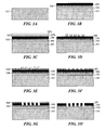
- FIGS. 3A-3H schematically show different stages of a method of manufacturing a converter element, for example a converter element as discussed with reference to FIG. 2A .
- the converter element is arranged for selectively converting impinging charged particles into photons.
- a substrate 101 is provided for supporting further layers of the sensor.
- the substrate 101 comprises a conversion material for converting charged particles into photons.
- Such conversion material may be a scintillating material.
- a suitable scintillating material may be a material comprising an yttrium aluminum garnet (YAG).
- a surface side of the substrate 101 arranged for reception of charged particles is coated with one or more layers, typically being metal layers.
- the layers comprise a first layer 103 comprising an electrically conductive material.
- the first layer 103 is substantially impermeable for ambient light, that is the layer is arranged for blocking background radiation. Such background light blocking layer enhances quality of the sensor by preventing background light from interfering with the light generated by the converter element.
- the first layer 103 is further substantially permeable for charged particle beamlets. For this reason, the first layer 103 generally has a thickness within the range of about 30 to about 80 nm. Suitable materials for the first metal include titanium and aluminum, Ti being preferred as less prone to oxidizing over time and hence more conducive to maintaining lasting surface uniformity of said layer.
- the layers comprise a second layer 104 comprising a second material.
- the second material is an etch stop material that serves the purpose of stopping an etching process, preferably for both wet etching and dry etching processes.
- the use of the second layer can result in improved etching quality, in particular if the material has a high etch sensitivity.
- the second layer may be particularly useful for the realization of sharper edges.
- a suitable material for the second metal is chrome.
- the layers further comprise a third layer 105 comprising a third material.
- the third material serves the purpose of blocking charged particle beamlets.
- a suitable material for the third material is a material that blocks charged particles as well as ambient light while having a layer of limited thickness.
- a suitable material is tungsten, in which case a suitable thickness would lie within the range of 50 to 500 nm. Such thickness is thick enough to sufficiently block incoming charged particles. On the other hand, such thickness has a negligible influence on effects like defocus and edge roughness.
- a resist layer 107 is provided on top of the number of layers 103, 104, 105.
- the resist layer 107 may be a single resist layer or, alternatively, a double resist layer comprising an upper layer 107a, and a lower layer 107b respectively. Further reference will be made to a single resist layer 107.
- the resist layer 107 is then patterned in correspondence to a first predetermined pattern. After patterning, the resist layer 107 undergoes developing and etching steps in a fashion generally known in the art. The etching is performed until the third layer 105 is exposed. An exemplary end result of patterning, developing and etching the resist layer 107 is schematically shown in FIG. 3D .
- the exposed third layer 105 is coated with a fourth layer 109, for example by means of evaporation, as is schematically shown in FIG. 3E .
- the fourth layer 109 is a metal layer.
- the fourth layer 109 may serve as an etch stopping layer and may improve etching quality.
- the layer 109 may comprise the same material as used in the second layer 104, for example chrome.
- the developed resist is removed by lift off such that the third layer 105 is exposed in accordance with a second predetermined pattern, as schematically shown in FIG. 3F .
- the second predetermined pattern is an inversion of the first predetermined pattern.
- the exposed third layer 105 is etched in accordance with the second predetermined pattern until the second layer 104 is exposed.
- a schematic drawing of the converter element at this stage of the manufacturing process is shown in FIG. 3G .
- the fourth layer 109 as well as the second layer 104 in accordance with the second predetermined pattern are removed, the latter one until the first layer 103 is exposed. Removal may be performed by techniques known in the art, for example etching.
- the resulting converter element is similar to the converter element described with reference to FIG. 2A .
- substrate 1 and layers 18, 20, and 21 in FIG. 2A correspond to substrate 101 and layers 105, 103, and 104 respectively.
- the invention has been described by reference to certain embodiments discussed above. It will be recognized that these embodiments are susceptible to various modifications and alternative forms well known to those of skill in the art. Further modifications in addition to those described above may be made to the structures and techniques described herein without departing from the scope of the invention. Accordingly, although specific embodiments have been described, these are examples only and are not limiting upon the scope of the invention, which is defined in the accompanying claims.
Landscapes
- Chemical & Material Sciences (AREA)
- Engineering & Computer Science (AREA)
- Analytical Chemistry (AREA)
- Nanotechnology (AREA)
- Crystallography & Structural Chemistry (AREA)
- Physics & Mathematics (AREA)
- Theoretical Computer Science (AREA)
- Mathematical Physics (AREA)
- Condensed Matter Physics & Semiconductors (AREA)
- General Physics & Mathematics (AREA)
- Manufacturing & Machinery (AREA)
- Measurement Of Radiation (AREA)
- Electron Sources, Ion Sources (AREA)
- Electron Beam Exposure (AREA)
Applications Claiming Priority (2)
| Application Number | Priority Date | Filing Date | Title |
|---|---|---|---|
| NL1037820A NL1037820C2 (en) | 2010-03-22 | 2010-03-22 | Lithography system, sensor, sensor surface element and method of manufacture. |
| PCT/EP2011/054372 WO2011117253A1 (en) | 2010-03-22 | 2011-03-22 | Lithography system, sensor, converter element and method of manufacture |
Publications (2)
| Publication Number | Publication Date |
|---|---|
| EP2550671A1 EP2550671A1 (en) | 2013-01-30 |
| EP2550671B1 true EP2550671B1 (en) | 2016-03-16 |
Family
ID=43034143
Family Applications (1)
| Application Number | Title | Priority Date | Filing Date |
|---|---|---|---|
| EP11709423.5A Active EP2550671B1 (en) | 2010-03-22 | 2011-03-22 | Lithography system, sensor, converter element and method of manufacture |
Country Status (9)
| Country | Link |
|---|---|
| US (2) | US8357906B2 (enExample) |
| EP (1) | EP2550671B1 (enExample) |
| JP (1) | JP5738973B2 (enExample) |
| KR (1) | KR101667770B1 (enExample) |
| CN (1) | CN102906850B (enExample) |
| NL (1) | NL1037820C2 (enExample) |
| RU (1) | RU2562126C2 (enExample) |
| TW (1) | TWI533350B (enExample) |
| WO (1) | WO2011117253A1 (enExample) |
Families Citing this family (11)
| Publication number | Priority date | Publication date | Assignee | Title |
|---|---|---|---|---|
| NL1037820C2 (en) | 2010-03-22 | 2011-09-23 | Mapper Lithography Ip Bv | Lithography system, sensor, sensor surface element and method of manufacture. |
| TWI545611B (zh) | 2010-11-13 | 2016-08-11 | 瑪波微影Ip公司 | 多射束曝光裝置以及用於決定其內的兩射束之間的距離之方法與感測器 |
| NL2008174C2 (en) * | 2012-01-24 | 2013-08-21 | Mapper Lithography Ip Bv | Device for spot size measurement at wafer level using a knife edge and a method for manufacturing such a device. |
| WO2013132064A2 (en) * | 2012-03-08 | 2013-09-12 | Mapper Lithography Ip B.V. | Charged particle lithography system with alignment sensor and beam measurement sensor |
| USRE49483E1 (en) * | 2012-05-14 | 2023-04-04 | Asml Netherlands B.V. | Method for determining a beamlet position and method for determining a distance between two beamlets in a multi-beamlet exposure apparatus |
| KR102126061B1 (ko) | 2013-11-28 | 2020-06-23 | 삼성전자주식회사 | 이미지 센서 및 그 제조 방법 |
| WO2017023574A1 (en) * | 2015-07-31 | 2017-02-09 | Pulsetor, Llc | Segmented detector for a charged particle beam device |
| US10714427B2 (en) | 2016-09-08 | 2020-07-14 | Asml Netherlands B.V. | Secure chips with serial numbers |
| NL2019503B1 (en) | 2016-09-08 | 2018-08-31 | Mapper Lithography Ip Bv | Fabricating unique chips using a charged particle multi-beamlet lithography system |
| US10418324B2 (en) | 2016-10-27 | 2019-09-17 | Asml Netherlands B.V. | Fabricating unique chips using a charged particle multi-beamlet lithography system |
| WO2018117275A1 (en) | 2016-12-23 | 2018-06-28 | Mapper Lithography Ip B.V. | Fabricating unique chips using a charged particle multi-beamlet lithography system |
Family Cites Families (32)
| Publication number | Priority date | Publication date | Assignee | Title |
|---|---|---|---|---|
| EP0049799B1 (en) * | 1980-10-09 | 1986-02-12 | Dai Nippon Insatsu Kabushiki Kaisha | Photomask blank and photomask |
| JPS62260335A (ja) * | 1986-05-06 | 1987-11-12 | Hitachi Ltd | パタ−ン検査方法および装置 |
| US4902898A (en) * | 1988-04-26 | 1990-02-20 | Microelectronics Center Of North Carolina | Wand optics column and associated array wand and charged particle source |
| US5136169A (en) | 1991-04-05 | 1992-08-04 | Massachusetts Institute Of Technology | Energy beam locating |
| JP2701764B2 (ja) * | 1994-12-28 | 1998-01-21 | 日本電気株式会社 | 荷電粒子ビームの寸法測定装置および測定方法 |
| US5872618A (en) | 1996-02-28 | 1999-02-16 | Nikon Corporation | Projection exposure apparatus |
| JPH09306400A (ja) * | 1996-05-15 | 1997-11-28 | Nippon Telegr & Teleph Corp <Ntt> | 電子ビ―ム計測用ナイフエッジ及びその製法並びに電子ビ―ム計測用ナイフエッジを用いた電子ビ―ム計測法 |
| US5910827A (en) * | 1997-02-26 | 1999-06-08 | Kwan; Katherine W. | Video signal decoding arrangement and method for improved error concealment |
| US5892230A (en) * | 1997-05-29 | 1999-04-06 | Massachusetts Institute Of Technology | Scintillating fiducial patterns |
| JPH11246300A (ja) | 1997-10-30 | 1999-09-14 | Canon Inc | チタンナノ細線、チタンナノ細線の製造方法、構造体及び電子放出素子 |
| US6429090B1 (en) * | 1999-03-03 | 2002-08-06 | Nikon Corporation | Fiducial mark bodies for charged-particle-beam (CPB) microlithography, methods for making same, and CPB microlithography apparatus comprising same |
| JP4505662B2 (ja) * | 1999-03-03 | 2010-07-21 | 株式会社ニコン | 基準マーク構造体、その製造方法及びそれを用いた荷電粒子線露光装置 |
| JP2000315785A (ja) | 1999-04-30 | 2000-11-14 | Canon Inc | ナノ構造体の製造方法及びナノ構造体デバイス |
| US6791094B1 (en) * | 1999-06-24 | 2004-09-14 | Varian Semiconductor Equipment Associates, Inc. | Method and apparatus for determining beam parallelism and direction |
| WO2001048560A1 (en) * | 1999-12-28 | 2001-07-05 | Toshiba Tec Kabushiki Kaisha | Image forming device and fixing device |
| DE10307545A1 (de) * | 2002-02-22 | 2003-11-06 | Hoya Corp | Zuschnitt für halbtonartige Phasenverschiebungsmaske und zugehörige Phasenverschiebungsmaske |
| CN1936703B (zh) * | 2002-06-18 | 2011-12-07 | Hoya株式会社 | 灰调掩模及其制造方法 |
| EP2302457B1 (en) | 2002-10-25 | 2016-03-30 | Mapper Lithography Ip B.V. | Lithography system |
| US6919570B2 (en) * | 2002-12-19 | 2005-07-19 | Advanced Electron Beams, Inc. | Electron beam sensor |
| JP2004251764A (ja) * | 2003-02-20 | 2004-09-09 | Tokyo Seimitsu Co Ltd | 電子ビーム像用tdiセンサ及びマスク検査装置 |
| JP4738723B2 (ja) * | 2003-08-06 | 2011-08-03 | キヤノン株式会社 | マルチ荷電粒子線描画装置、荷電粒子線の電流の測定方法及びデバイス製造方法 |
| US20050088633A1 (en) | 2003-10-24 | 2005-04-28 | Intel Corporation | Composite optical lithography method for patterning lines of unequal width |
| JP3962778B2 (ja) | 2004-06-02 | 2007-08-22 | 株式会社日立ハイテクノロジーズ | 電子ビーム検出器、並びにそれを用いた電子ビーム描画方法及び電子ビーム描画装置 |
| CN1907191A (zh) | 2005-07-25 | 2007-02-07 | 株式会社泉精器制作所 | 饮料制作器 |
| JP2007042803A (ja) | 2005-08-02 | 2007-02-15 | Honda Motor Co Ltd | イオン注入マスクおよびその製造方法、並びにイオン注入マスクを用いた炭化珪素半導体装置およびその製造方法 |
| TWI407260B (zh) * | 2005-09-15 | 2013-09-01 | Mapper Lithography Ip Bv | 微影系統,感測器及測量方法 |
| US7868300B2 (en) * | 2005-09-15 | 2011-01-11 | Mapper Lithography Ip B.V. | Lithography system, sensor and measuring method |
| KR101433385B1 (ko) * | 2005-09-15 | 2014-08-26 | 마퍼 리쏘그라피 아이피 비.브이. | 리소그래피 시스템, 센서 및 측정 방법 |
| US7521685B2 (en) | 2006-01-18 | 2009-04-21 | General Electric Company | Structured scintillator and systems employing structured scintillators |
| JP2008041890A (ja) * | 2006-08-04 | 2008-02-21 | Canon Inc | マルチ荷電粒子ビームの計測方法、露光装置、及びデバイス製造方法 |
| JP5301312B2 (ja) * | 2008-03-21 | 2013-09-25 | 株式会社ニューフレアテクノロジー | 荷電粒子ビーム描画装置の較正用基板及び描画方法 |
| NL1037820C2 (en) | 2010-03-22 | 2011-09-23 | Mapper Lithography Ip Bv | Lithography system, sensor, sensor surface element and method of manufacture. |
-
2010
- 2010-03-22 NL NL1037820A patent/NL1037820C2/en not_active IP Right Cessation
-
2011
- 2011-03-21 TW TW100109513A patent/TWI533350B/zh active
- 2011-03-22 WO PCT/EP2011/054372 patent/WO2011117253A1/en not_active Ceased
- 2011-03-22 RU RU2012144624/07A patent/RU2562126C2/ru active
- 2011-03-22 EP EP11709423.5A patent/EP2550671B1/en active Active
- 2011-03-22 CN CN201180025381.3A patent/CN102906850B/zh active Active
- 2011-03-22 US US13/053,488 patent/US8357906B2/en not_active Ceased
- 2011-03-22 JP JP2013500473A patent/JP5738973B2/ja active Active
- 2011-03-22 KR KR1020127027493A patent/KR101667770B1/ko active Active
-
2015
- 2015-01-22 US US14/602,294 patent/USRE47287E1/en active Active
Also Published As
| Publication number | Publication date |
|---|---|
| USRE47287E1 (en) | 2019-03-12 |
| JP5738973B2 (ja) | 2015-06-24 |
| KR20130067252A (ko) | 2013-06-21 |
| NL1037820C2 (en) | 2011-09-23 |
| CN102906850B (zh) | 2015-09-09 |
| RU2562126C2 (ru) | 2015-09-10 |
| RU2012144624A (ru) | 2014-04-27 |
| US8357906B2 (en) | 2013-01-22 |
| WO2011117253A1 (en) | 2011-09-29 |
| US20110253900A1 (en) | 2011-10-20 |
| EP2550671A1 (en) | 2013-01-30 |
| JP2013522923A (ja) | 2013-06-13 |
| TWI533350B (zh) | 2016-05-11 |
| TW201301332A (zh) | 2013-01-01 |
| CN102906850A (zh) | 2013-01-30 |
| KR101667770B1 (ko) | 2016-10-19 |
Similar Documents
| Publication | Publication Date | Title |
|---|---|---|
| EP2550671B1 (en) | Lithography system, sensor, converter element and method of manufacture | |
| KR101959945B1 (ko) | 빔렛 위치를 결정하기 위한 방법 및 멀티 빔렛 노출 장치에서 2개의 빔렛들 간의 거리를 결정하기 위한 방법 | |
| JP5882348B2 (ja) | マルチ小ビーム露光装置における2つの小ビーム間の距離を決定する方法 | |
| US7868300B2 (en) | Lithography system, sensor and measuring method | |
| JP5199097B2 (ja) | リソグラフィシステム、センサ、測定方法 | |
| US7560693B2 (en) | Electron-beam size measuring apparatus and size measuring method with electron beams | |
| JP6237048B2 (ja) | パターン計測方法及び装置 |
Legal Events
| Date | Code | Title | Description |
|---|---|---|---|
| PUAI | Public reference made under article 153(3) epc to a published international application that has entered the european phase |
Free format text: ORIGINAL CODE: 0009012 |
|
| 17P | Request for examination filed |
Effective date: 20121005 |
|
| AK | Designated contracting states |
Kind code of ref document: A1 Designated state(s): AL AT BE BG CH CY CZ DE DK EE ES FI FR GB GR HR HU IE IS IT LI LT LU LV MC MK MT NL NO PL PT RO RS SE SI SK SM TR |
|
| DAX | Request for extension of the european patent (deleted) | ||
| GRAP | Despatch of communication of intention to grant a patent |
Free format text: ORIGINAL CODE: EPIDOSNIGR1 |
|
| INTG | Intention to grant announced |
Effective date: 20150430 |
|
| GRAP | Despatch of communication of intention to grant a patent |
Free format text: ORIGINAL CODE: EPIDOSNIGR1 |
|
| INTG | Intention to grant announced |
Effective date: 20150914 |
|
| GRAS | Grant fee paid |
Free format text: ORIGINAL CODE: EPIDOSNIGR3 |
|
| GRAA | (expected) grant |
Free format text: ORIGINAL CODE: 0009210 |
|
| AK | Designated contracting states |
Kind code of ref document: B1 Designated state(s): AL AT BE BG CH CY CZ DE DK EE ES FI FR GB GR HR HU IE IS IT LI LT LU LV MC MK MT NL NO PL PT RO RS SE SI SK SM TR |
|
| REG | Reference to a national code |
Ref country code: GB Ref legal event code: FG4D |
|
| REG | Reference to a national code |
Ref country code: FR Ref legal event code: PLFP Year of fee payment: 6 |
|
| REG | Reference to a national code |
Ref country code: CH Ref legal event code: EP |
|
| REG | Reference to a national code |
Ref country code: IE Ref legal event code: FG4D |
|
| REG | Reference to a national code |
Ref country code: AT Ref legal event code: REF Ref document number: 781875 Country of ref document: AT Kind code of ref document: T Effective date: 20160415 |
|
| REG | Reference to a national code |
Ref country code: DE Ref legal event code: R096 Ref document number: 602011024030 Country of ref document: DE |
|
| REG | Reference to a national code |
Ref country code: NL Ref legal event code: FP |
|
| REG | Reference to a national code |
Ref country code: LT Ref legal event code: MG4D |
|
| PG25 | Lapsed in a contracting state [announced via postgrant information from national office to epo] |
Ref country code: FI Free format text: LAPSE BECAUSE OF FAILURE TO SUBMIT A TRANSLATION OF THE DESCRIPTION OR TO PAY THE FEE WITHIN THE PRESCRIBED TIME-LIMIT Effective date: 20160316 Ref country code: GR Free format text: LAPSE BECAUSE OF FAILURE TO SUBMIT A TRANSLATION OF THE DESCRIPTION OR TO PAY THE FEE WITHIN THE PRESCRIBED TIME-LIMIT Effective date: 20160617 Ref country code: NO Free format text: LAPSE BECAUSE OF FAILURE TO SUBMIT A TRANSLATION OF THE DESCRIPTION OR TO PAY THE FEE WITHIN THE PRESCRIBED TIME-LIMIT Effective date: 20160616 Ref country code: HR Free format text: LAPSE BECAUSE OF FAILURE TO SUBMIT A TRANSLATION OF THE DESCRIPTION OR TO PAY THE FEE WITHIN THE PRESCRIBED TIME-LIMIT Effective date: 20160316 |
|
| PG25 | Lapsed in a contracting state [announced via postgrant information from national office to epo] |
Ref country code: BE Free format text: LAPSE BECAUSE OF NON-PAYMENT OF DUE FEES Effective date: 20160331 Ref country code: LT Free format text: LAPSE BECAUSE OF FAILURE TO SUBMIT A TRANSLATION OF THE DESCRIPTION OR TO PAY THE FEE WITHIN THE PRESCRIBED TIME-LIMIT Effective date: 20160316 Ref country code: LV Free format text: LAPSE BECAUSE OF FAILURE TO SUBMIT A TRANSLATION OF THE DESCRIPTION OR TO PAY THE FEE WITHIN THE PRESCRIBED TIME-LIMIT Effective date: 20160316 Ref country code: RS Free format text: LAPSE BECAUSE OF FAILURE TO SUBMIT A TRANSLATION OF THE DESCRIPTION OR TO PAY THE FEE WITHIN THE PRESCRIBED TIME-LIMIT Effective date: 20160316 Ref country code: SE Free format text: LAPSE BECAUSE OF FAILURE TO SUBMIT A TRANSLATION OF THE DESCRIPTION OR TO PAY THE FEE WITHIN THE PRESCRIBED TIME-LIMIT Effective date: 20160316 |
|
| PG25 | Lapsed in a contracting state [announced via postgrant information from national office to epo] |
Ref country code: PL Free format text: LAPSE BECAUSE OF FAILURE TO SUBMIT A TRANSLATION OF THE DESCRIPTION OR TO PAY THE FEE WITHIN THE PRESCRIBED TIME-LIMIT Effective date: 20160316 Ref country code: IS Free format text: LAPSE BECAUSE OF FAILURE TO SUBMIT A TRANSLATION OF THE DESCRIPTION OR TO PAY THE FEE WITHIN THE PRESCRIBED TIME-LIMIT Effective date: 20160716 Ref country code: EE Free format text: LAPSE BECAUSE OF FAILURE TO SUBMIT A TRANSLATION OF THE DESCRIPTION OR TO PAY THE FEE WITHIN THE PRESCRIBED TIME-LIMIT Effective date: 20160316 |
|
| REG | Reference to a national code |
Ref country code: CH Ref legal event code: PL |
|
| PG25 | Lapsed in a contracting state [announced via postgrant information from national office to epo] |
Ref country code: ES Free format text: LAPSE BECAUSE OF FAILURE TO SUBMIT A TRANSLATION OF THE DESCRIPTION OR TO PAY THE FEE WITHIN THE PRESCRIBED TIME-LIMIT Effective date: 20160316 Ref country code: SK Free format text: LAPSE BECAUSE OF FAILURE TO SUBMIT A TRANSLATION OF THE DESCRIPTION OR TO PAY THE FEE WITHIN THE PRESCRIBED TIME-LIMIT Effective date: 20160316 Ref country code: SM Free format text: LAPSE BECAUSE OF FAILURE TO SUBMIT A TRANSLATION OF THE DESCRIPTION OR TO PAY THE FEE WITHIN THE PRESCRIBED TIME-LIMIT Effective date: 20160316 Ref country code: PT Free format text: LAPSE BECAUSE OF FAILURE TO SUBMIT A TRANSLATION OF THE DESCRIPTION OR TO PAY THE FEE WITHIN THE PRESCRIBED TIME-LIMIT Effective date: 20160718 Ref country code: RO Free format text: LAPSE BECAUSE OF FAILURE TO SUBMIT A TRANSLATION OF THE DESCRIPTION OR TO PAY THE FEE WITHIN THE PRESCRIBED TIME-LIMIT Effective date: 20160316 Ref country code: CZ Free format text: LAPSE BECAUSE OF FAILURE TO SUBMIT A TRANSLATION OF THE DESCRIPTION OR TO PAY THE FEE WITHIN THE PRESCRIBED TIME-LIMIT Effective date: 20160316 |
|
| REG | Reference to a national code |
Ref country code: DE Ref legal event code: R097 Ref document number: 602011024030 Country of ref document: DE |
|
| PG25 | Lapsed in a contracting state [announced via postgrant information from national office to epo] |
Ref country code: BE Free format text: LAPSE BECAUSE OF FAILURE TO SUBMIT A TRANSLATION OF THE DESCRIPTION OR TO PAY THE FEE WITHIN THE PRESCRIBED TIME-LIMIT Effective date: 20160316 Ref country code: IT Free format text: LAPSE BECAUSE OF FAILURE TO SUBMIT A TRANSLATION OF THE DESCRIPTION OR TO PAY THE FEE WITHIN THE PRESCRIBED TIME-LIMIT Effective date: 20160316 |
|
| PLBE | No opposition filed within time limit |
Free format text: ORIGINAL CODE: 0009261 |
|
| STAA | Information on the status of an ep patent application or granted ep patent |
Free format text: STATUS: NO OPPOSITION FILED WITHIN TIME LIMIT |
|
| PG25 | Lapsed in a contracting state [announced via postgrant information from national office to epo] |
Ref country code: LI Free format text: LAPSE BECAUSE OF NON-PAYMENT OF DUE FEES Effective date: 20160331 Ref country code: DK Free format text: LAPSE BECAUSE OF FAILURE TO SUBMIT A TRANSLATION OF THE DESCRIPTION OR TO PAY THE FEE WITHIN THE PRESCRIBED TIME-LIMIT Effective date: 20160316 Ref country code: CH Free format text: LAPSE BECAUSE OF NON-PAYMENT OF DUE FEES Effective date: 20160331 |
|
| 26N | No opposition filed |
Effective date: 20161219 |
|
| PG25 | Lapsed in a contracting state [announced via postgrant information from national office to epo] |
Ref country code: BG Free format text: LAPSE BECAUSE OF FAILURE TO SUBMIT A TRANSLATION OF THE DESCRIPTION OR TO PAY THE FEE WITHIN THE PRESCRIBED TIME-LIMIT Effective date: 20160616 |
|
| REG | Reference to a national code |
Ref country code: FR Ref legal event code: PLFP Year of fee payment: 7 |
|
| PG25 | Lapsed in a contracting state [announced via postgrant information from national office to epo] |
Ref country code: SI Free format text: LAPSE BECAUSE OF FAILURE TO SUBMIT A TRANSLATION OF THE DESCRIPTION OR TO PAY THE FEE WITHIN THE PRESCRIBED TIME-LIMIT Effective date: 20160316 |
|
| PG25 | Lapsed in a contracting state [announced via postgrant information from national office to epo] |
Ref country code: MT Free format text: LAPSE BECAUSE OF FAILURE TO SUBMIT A TRANSLATION OF THE DESCRIPTION OR TO PAY THE FEE WITHIN THE PRESCRIBED TIME-LIMIT Effective date: 20160316 |
|
| REG | Reference to a national code |
Ref country code: AT Ref legal event code: UEP Ref document number: 781875 Country of ref document: AT Kind code of ref document: T Effective date: 20160316 |
|
| REG | Reference to a national code |
Ref country code: FR Ref legal event code: PLFP Year of fee payment: 8 |
|
| PG25 | Lapsed in a contracting state [announced via postgrant information from national office to epo] |
Ref country code: CY Free format text: LAPSE BECAUSE OF FAILURE TO SUBMIT A TRANSLATION OF THE DESCRIPTION OR TO PAY THE FEE WITHIN THE PRESCRIBED TIME-LIMIT Effective date: 20160316 Ref country code: HU Free format text: LAPSE BECAUSE OF FAILURE TO SUBMIT A TRANSLATION OF THE DESCRIPTION OR TO PAY THE FEE WITHIN THE PRESCRIBED TIME-LIMIT; INVALID AB INITIO Effective date: 20110322 |
|
| PG25 | Lapsed in a contracting state [announced via postgrant information from national office to epo] |
Ref country code: TR Free format text: LAPSE BECAUSE OF FAILURE TO SUBMIT A TRANSLATION OF THE DESCRIPTION OR TO PAY THE FEE WITHIN THE PRESCRIBED TIME-LIMIT Effective date: 20160316 Ref country code: MC Free format text: LAPSE BECAUSE OF FAILURE TO SUBMIT A TRANSLATION OF THE DESCRIPTION OR TO PAY THE FEE WITHIN THE PRESCRIBED TIME-LIMIT Effective date: 20160316 Ref country code: MT Free format text: LAPSE BECAUSE OF FAILURE TO SUBMIT A TRANSLATION OF THE DESCRIPTION OR TO PAY THE FEE WITHIN THE PRESCRIBED TIME-LIMIT Effective date: 20160331 Ref country code: LU Free format text: LAPSE BECAUSE OF NON-PAYMENT OF DUE FEES Effective date: 20160322 Ref country code: MK Free format text: LAPSE BECAUSE OF FAILURE TO SUBMIT A TRANSLATION OF THE DESCRIPTION OR TO PAY THE FEE WITHIN THE PRESCRIBED TIME-LIMIT Effective date: 20160316 |
|
| PG25 | Lapsed in a contracting state [announced via postgrant information from national office to epo] |
Ref country code: AL Free format text: LAPSE BECAUSE OF FAILURE TO SUBMIT A TRANSLATION OF THE DESCRIPTION OR TO PAY THE FEE WITHIN THE PRESCRIBED TIME-LIMIT Effective date: 20160316 |
|
| REG | Reference to a national code |
Ref country code: NL Ref legal event code: PD Owner name: ASML NETHERLANDS B.V.; NL Free format text: DETAILS ASSIGNMENT: CHANGE OF OWNER(S), ASSIGNMENT; FORMER OWNER NAME: MAPPER LITHOGRAPHY IP B.V. Effective date: 20190425 |
|
| PGFP | Annual fee paid to national office [announced via postgrant information from national office to epo] |
Ref country code: IE Payment date: 20220321 Year of fee payment: 12 Ref country code: GB Payment date: 20220322 Year of fee payment: 12 |
|
| P01 | Opt-out of the competence of the unified patent court (upc) registered |
Effective date: 20230403 |
|
| GBPC | Gb: european patent ceased through non-payment of renewal fee |
Effective date: 20230322 |
|
| REG | Reference to a national code |
Ref country code: IE Ref legal event code: MM4A |
|
| PG25 | Lapsed in a contracting state [announced via postgrant information from national office to epo] |
Ref country code: GB Free format text: LAPSE BECAUSE OF NON-PAYMENT OF DUE FEES Effective date: 20230322 |
|
| PG25 | Lapsed in a contracting state [announced via postgrant information from national office to epo] |
Ref country code: IE Free format text: LAPSE BECAUSE OF NON-PAYMENT OF DUE FEES Effective date: 20230322 Ref country code: GB Free format text: LAPSE BECAUSE OF NON-PAYMENT OF DUE FEES Effective date: 20230322 |
|
| PGFP | Annual fee paid to national office [announced via postgrant information from national office to epo] |
Ref country code: DE Payment date: 20260320 Year of fee payment: 16 |
|
| PGFP | Annual fee paid to national office [announced via postgrant information from national office to epo] |
Ref country code: AT Payment date: 20260318 Year of fee payment: 16 |
|
| PGFP | Annual fee paid to national office [announced via postgrant information from national office to epo] |
Ref country code: NL Payment date: 20260323 Year of fee payment: 16 |
|
| PGFP | Annual fee paid to national office [announced via postgrant information from national office to epo] |
Ref country code: FR Payment date: 20260323 Year of fee payment: 16 |