EP2549299B1 - Radiation detection apparatus and detection system including same - Google Patents
Radiation detection apparatus and detection system including same Download PDFInfo
- Publication number
- EP2549299B1 EP2549299B1 EP12173101.2A EP12173101A EP2549299B1 EP 2549299 B1 EP2549299 B1 EP 2549299B1 EP 12173101 A EP12173101 A EP 12173101A EP 2549299 B1 EP2549299 B1 EP 2549299B1
- Authority
- EP
- European Patent Office
- Prior art keywords
- unit
- thin
- film transistor
- circuit
- input unit
- Prior art date
- Legal status (The legal status is an assumption and is not a legal conclusion. Google has not performed a legal analysis and makes no representation as to the accuracy of the status listed.)
- Active
Links
- 238000001514 detection method Methods 0.000 title claims description 57
- 230000005855 radiation Effects 0.000 title claims description 21
- 239000010409 thin film Substances 0.000 claims description 201
- 239000003990 capacitor Substances 0.000 claims description 47
- 238000006243 chemical reaction Methods 0.000 claims description 25
- 239000000758 substrate Substances 0.000 claims description 18
- 238000000034 method Methods 0.000 claims description 8
- 230000000977 initiatory effect Effects 0.000 claims description 5
- 230000005540 biological transmission Effects 0.000 claims description 2
- 239000011159 matrix material Substances 0.000 claims description 2
- 239000004065 semiconductor Substances 0.000 description 22
- 239000012535 impurity Substances 0.000 description 9
- 230000007423 decrease Effects 0.000 description 6
- 239000000463 material Substances 0.000 description 6
- 229910021420 polycrystalline silicon Inorganic materials 0.000 description 6
- 229910021417 amorphous silicon Inorganic materials 0.000 description 5
- 238000003384 imaging method Methods 0.000 description 5
- 238000004519 manufacturing process Methods 0.000 description 5
- 238000010586 diagram Methods 0.000 description 4
- 238000005516 engineering process Methods 0.000 description 4
- 230000003071 parasitic effect Effects 0.000 description 4
- 239000010408 film Substances 0.000 description 2
- 239000011521 glass Substances 0.000 description 2
- 238000007689 inspection Methods 0.000 description 2
- 229910021421 monocrystalline silicon Inorganic materials 0.000 description 2
- 239000002245 particle Substances 0.000 description 2
- 238000002161 passivation Methods 0.000 description 2
- 239000007787 solid Substances 0.000 description 2
- XUIMIQQOPSSXEZ-UHFFFAOYSA-N Silicon Chemical compound [Si] XUIMIQQOPSSXEZ-UHFFFAOYSA-N 0.000 description 1
- JJWKPURADFRFRB-UHFFFAOYSA-N carbonyl sulfide Chemical compound O=C=S JJWKPURADFRFRB-UHFFFAOYSA-N 0.000 description 1
- 239000004020 conductor Substances 0.000 description 1
- 230000008878 coupling Effects 0.000 description 1
- 238000010168 coupling process Methods 0.000 description 1
- 238000005859 coupling reaction Methods 0.000 description 1
- 238000007667 floating Methods 0.000 description 1
- 230000014509 gene expression Effects 0.000 description 1
- 229910052732 germanium Inorganic materials 0.000 description 1
- GNPVGFCGXDBREM-UHFFFAOYSA-N germanium atom Chemical compound [Ge] GNPVGFCGXDBREM-UHFFFAOYSA-N 0.000 description 1
- 239000011810 insulating material Substances 0.000 description 1
- 239000004973 liquid crystal related substance Substances 0.000 description 1
- 230000003287 optical effect Effects 0.000 description 1
- 229920001296 polysiloxane Polymers 0.000 description 1
- 230000005258 radioactive decay Effects 0.000 description 1
- 229910052710 silicon Inorganic materials 0.000 description 1
- 239000010703 silicon Substances 0.000 description 1
Images


Classifications
-
- H—ELECTRICITY
- H04—ELECTRIC COMMUNICATION TECHNIQUE
- H04N—PICTORIAL COMMUNICATION, e.g. TELEVISION
- H04N5/00—Details of television systems
- H04N5/30—Transforming light or analogous information into electric information
- H04N5/32—Transforming X-rays
-
- H—ELECTRICITY
- H04—ELECTRIC COMMUNICATION TECHNIQUE
- H04N—PICTORIAL COMMUNICATION, e.g. TELEVISION
- H04N25/00—Circuitry of solid-state image sensors [SSIS]; Control thereof
- H04N25/70—SSIS architectures; Circuits associated therewith
- H04N25/71—Charge-coupled device [CCD] sensors; Charge-transfer registers specially adapted for CCD sensors
- H04N25/745—Circuitry for generating timing or clock signals
-
- H—ELECTRICITY
- H01—ELECTRIC ELEMENTS
- H01L—SEMICONDUCTOR DEVICES NOT COVERED BY CLASS H10
- H01L27/00—Devices consisting of a plurality of semiconductor or other solid-state components formed in or on a common substrate
- H01L27/14—Devices consisting of a plurality of semiconductor or other solid-state components formed in or on a common substrate including semiconductor components sensitive to infrared radiation, light, electromagnetic radiation of shorter wavelength or corpuscular radiation and specially adapted either for the conversion of the energy of such radiation into electrical energy or for the control of electrical energy by such radiation
- H01L27/144—Devices controlled by radiation
- H01L27/146—Imager structures
- H01L27/14601—Structural or functional details thereof
- H01L27/14609—Pixel-elements with integrated switching, control, storage or amplification elements
-
- H—ELECTRICITY
- H01—ELECTRIC ELEMENTS
- H01L—SEMICONDUCTOR DEVICES NOT COVERED BY CLASS H10
- H01L27/00—Devices consisting of a plurality of semiconductor or other solid-state components formed in or on a common substrate
- H01L27/14—Devices consisting of a plurality of semiconductor or other solid-state components formed in or on a common substrate including semiconductor components sensitive to infrared radiation, light, electromagnetic radiation of shorter wavelength or corpuscular radiation and specially adapted either for the conversion of the energy of such radiation into electrical energy or for the control of electrical energy by such radiation
- H01L27/144—Devices controlled by radiation
- H01L27/146—Imager structures
- H01L27/14643—Photodiode arrays; MOS imagers
- H01L27/14658—X-ray, gamma-ray or corpuscular radiation imagers
- H01L27/14663—Indirect radiation imagers, e.g. using luminescent members
-
- H—ELECTRICITY
- H01—ELECTRIC ELEMENTS
- H01L—SEMICONDUCTOR DEVICES NOT COVERED BY CLASS H10
- H01L27/00—Devices consisting of a plurality of semiconductor or other solid-state components formed in or on a common substrate
- H01L27/14—Devices consisting of a plurality of semiconductor or other solid-state components formed in or on a common substrate including semiconductor components sensitive to infrared radiation, light, electromagnetic radiation of shorter wavelength or corpuscular radiation and specially adapted either for the conversion of the energy of such radiation into electrical energy or for the control of electrical energy by such radiation
- H01L27/144—Devices controlled by radiation
- H01L27/146—Imager structures
- H01L27/14683—Processes or apparatus peculiar to the manufacture or treatment of these devices or parts thereof
- H01L27/14692—Thin film technologies, e.g. amorphous, poly, micro- or nanocrystalline silicon
Definitions
- the present invention relates to a radiation detection apparatus according to claim 1 and a detection system that are applied to medical image diagnostic apparatuses, nondestructive inspection apparatuses, analytical apparatuses that use radiation, and the like.
- a technique for manufacturing thin-film semiconductors is utilized in the manufacture of a detection apparatus including an array of pixels (pixel array).
- switch elements such as thin-film transistors (TFTs) and conversion elements such as photoelectric conversion elements are combined.
- TFTs thin-film transistors
- a substrate having a size of 43 ⁇ 43 cm on which pixels are arranged in an array at a pitch of 150 to 200 ⁇ m has been used to manufacture a radiation detection apparatus.
- a driving circuit drives the pixel array in units of rows through driving wires, and a read circuit outputs signals from the pixel array driven in units of rows parallel to one another through signal wires as serial signals.
- the driving and read circuits are typically prepared in an integrated circuit composed of monocrystalline silicon, and subsequently mounted onto the substrate using chip-on-glass (CoG) technology to configure the detection apparatus.
- CoG chip-on-glass
- the pitch of the pixels is desired to be smaller while the size of the substrate in the related art remains the same. More specifically, a pixel array having a pitch of 50 to 80 ⁇ m is expected. Therefore, it would be difficult to mount, using chip-on-glass technology, the driving circuit prepared in the integrated circuit composed of monocrystalline silicon on the substrate on which the pixel array is provided.
- a system-on-panel technology is expected in which the driving circuit and the like are formed integrally on the substrate as a unit using a TFT process, in order to reduce the number of components used, and to increase the area of the substrate occupied by the pixel array.
- the first input unit is a portion to which a start signal or an output signal of a unit circuit in the previous stage is input
- the output unit is a portion connected to a driving wire to supply an output signal including conducting voltage and non-conducting voltage of a switch element to the driving wire.
- the second input unit is a portion to which a clock signal is input
- the third input unit is a portion to which the non-conducting voltage of the switch element is input
- the fourth input unit is a portion to which a reset signal or an output signal of a unit circuit in the next stage is input.
- Each unit circuit also includes a first capacitor, one end of which is connected to the output unit, a first thin-film transistor connected between the first input unit and another end of the first capacitor in series with the first capacitor, and a second thin-film transistor provided between the second input unit and the output unit. Either a source or a drain and a gate of the first thin-film transistor are connected to the first input unit, and the other of the source and the drain of the first thin-film transistor is connected to the other end of the first capacitor at a first node P.
- a gate of the second thin-film transistor is connected to the first node P, either a source or a drain of the second thin-film transistor is connected to the second input unit, and the other of the source and the drain of the second thin-film transistor is connected to the output unit.
- Each unit circuit also includes a third thin-film transistor connected between the third input unit and the other end of the first capacitor in series with the first capacitor and a fourth thin-film transistor provided between the third input unit and the output unit.
- a gate of the third thin-film transistor is connected to a second node Q, either a source or a drain of the third thin-film transistor is connected to the third input unit, and the other of the source and the drain of the third thin-film transistor is connected to the other end of the first capacitor at the first node P.
- a gate of the fourth thin-film transistor is connected to the second node Q, either a source or a drain of the fourth thin-film transistor is connected to the third input unit, and the other of the source and the drain of the fourth-thin film transistor is connected to the output unit.
- Each unit circuit also includes a second capacitor provided between the third input unit and the gate of the fourth thin-film transistor.
- each unit circuit includes a fifth thin-film transistor provided between the fourth input unit and the gates of the second and fourth thin-film transistors and a sixth thin-film transistor provided parallel to the second capacitor.
- One end of the second capacitor is connected to the third input unit, and another end of the second capacitor is connected to the gate of the fourth thin-film transistor at the second node Q.
- Either a source or a drain and a gate of the fifth thin-film transistor are connected to the fourth input unit, and the other of the source and the drain of the fifth thin-film transistor is connected to the second node Q.
- a gate of the sixth thin-film transistor is connected to the first input unit, either a source or a drain of the sixth thin-film transistor is connected to the third input unit, and the other of the source and the drain of the sixth thin-film transistor is connected to the second node Q.
- the threshold voltage of each of the first to sixth thin-film transistors is denoted by Vth
- the maximum and minimum values of voltage of signals input to the components of the unit circuit other than the third input unit are denoted by V DD and V SS , respectively.
- the non-conducting voltage supplied to the second input unit is also denoted by V SS .
- this unit circuit can execute a so-called bootstrap operation, in which the maximum value of voltage of the clock signal input to the second input unit, namely V DD , is output by the first and second thin-film transistors and the first capacitor.
- the unit circuit can output the non-conducting voltage using the fifth and sixth thin-film transistors and the second capacitor. That is, when the unit circuit has been selected, the first and second thin-film transistors and the first capacitor serve as a circuit that supplies the maximum value of voltage of the clock signal input to the second input unit, namely V DD , to the output unit as the conducting voltage of the switch element of a pixel.
- the third to sixth thin-film transistors and the second capacitor serve as a circuit that supplies the non-conducting voltage V SS to the output unit.
- a circuit is said to "float" when the circuit is not grounded and stays at some potential other than a ground reference potential; that is, the conductor(s) of the circuit are isolated from ground.
- a floating circuit can have safety issues because there is no low-impedance path to ground.
- this type of circuit can also help isolate a system from interference problems, for example.
- the second input unit and the output unit directly form capacitive coupling due to gate-to-drain capacitance Cgd or gate-to-source capacitance Cgs and the parasitic capacitance of a region in which a wire that supplies the clock signal and a driving wire intersects.
- the driving wire has parasitic capacitance in the region in which the driving wire intersects with the signal wire, and the variation in the potential of the driving wire affects the potential of the signal wire through the parasitic capacitance, thereby mixing the variation in the potential of the driving wire into a signal output from a pixel through the signal wire. Therefore, a noise component caused by the variation in the potential of the driving wire becomes large in the signal output from the pixel through the signal wire, and accordingly the signal-to-noise ratio (S/N) of a signal obtained from the detection apparatus can undesirably decrease.
- S/N signal-to-noise ratio
- the present invention provides a detection apparatus in which a driving circuit is formed on a substrate as a unit using a TFT process and that can suppress a decrease in the S/N ratio caused by variation in the potential of a driving wire.
- the present invention in its first aspect provides a detection apparatus as specified in claims 1 to 10.
- the present invention in its second aspect provides a detection system as specified in claim 11.
- the first aspect of the present invention it is possible to provide a detection apparatus in which a driving circuit is formed on a substrate as a unit using a TFT process and that can suppress a decrease in the S/N ratio caused by variation in the potential of a driving wire.
- Variation in the potential of driving wires is a new challenge that can be posed by a detection apparatus.
- the period of time for which non-conducting voltage needs to be remain unchanged (constant) when a unit circuit has not been selected is short, namely 1/30 to 1/60 second, and therefore it is unlikely that an output unit of the unit circuit floats.
- the period of time for which non-conducting voltage needs to remain unchanged (constant) when a unit circuit has not been selected can be long in a certain operation mode, namely 1 to 3 seconds, and therefore an output unit of the unit circuit can float.
- radiation herein includes alpha rays, beta rays, and gamma rays, which are beams configured by particles (include photons) discharged as a result of radioactive decay, as well as beams having visible light, X-rays, particle beams, and cosmic rays, among others.
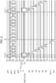
- Fig. 1A illustrates a schematic equivalent circuit of the detection apparatus
- Fig. 1B illustrates a schematic equivalent circuit of a unit circuit provided in a driving circuit unit of the detection apparatus.
- a detection apparatus 100 includes a pixel array in which a plurality of pixels 110 are provided on an insulating substrate 101 in a matrix of m rows by n columns.
- the pixel array has m rows and n columns.
- Each pixel 110 includes a conversion element 111 that converts radiation or light into electric charge and a switch element 112 that outputs an electrical signal according to the converted electric charge. Either a source or a drain of the switch element 112 is electrically connected to a first electrode of the conversion element 111, and a second electrode of the conversion element 111 is electrically connected to an electrode wire 180.
- the electrode wire 180 is connected to a power supply unit 140 through a connection terminal VS.
- a signal wire 170 is electrically connected to the other of the source and the drain of the switch element 112.
- a plurality of (n) signal wires 170 are arranged in a row direction, and each signal wire 170 is connected to the other of the sources and the drains of the plurality of switch elements 112 arranged in a column direction and to an external read circuit unit 130 through one of connection terminals S1 to Sn.
- a driving wire 160 is electrically connected to a control electrode of each switch element 112.
- a plurality of (m) driving wires 160 are arranged in the column direction, and each driving wire 160 is connected to gates of the plurality of switch elements 112 arranged in the row direction and to a driving circuit unit 120 provided on the insulating substrate 101.
- the driving circuit unit 120 is connected to the power supply unit 140 through a connection terminal V SS , and to a control unit 150 through connection terminals CL1, CL2, ST, and LH.
- the power supply unit 140 supplies voltage V S to be supplied to the conversion elements 111 to the electrode wire 180 and non-conducting voltage V SS of the switch elements 112 to the driving circuit unit 120.
- the control unit 150 supplies, to the driving circuit unit 120, a start signal ⁇ ST for the driving circuit unit 120 to begin to supply conducting voltage V DD of the switch elements 112 to the driving wires 160.
- the control unit 150 also supplies clock signals ⁇ CL1 and ⁇ CL2 that define the timing of the supply of the conducting voltage V DD and the non-conducting voltage V SS to the driving circuit unit 120.
- the control unit 150 also supplies, to the driving circuit unit 120, a reset signal for terminating the supply of the conducting voltage V DD to the driving wire 160 and a control signal ⁇ LH for continuing to supply the non-conducting voltage V SS to the driving wire 160.
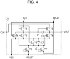
- the driving circuit unit 120 includes a unit circuit 121, which is provided on the insulating substrate 101, for each driving wire 160. As a whole, the driving circuit unit 120 includes a plurality of (m) unit circuits 121 corresponding to the plurality of driving wires 160. Each unit circuit 121 supplies an output signal Vg including the conducting voltage V DD and the non-conducting voltage V SS to each driving wire 160.
- each unit circuit 121 includes an output unit VOUT, a first input unit SET, a second input unit CLK, a third input unit VSS, a fourth input unit RESET, and a fifth input unit LHLD.
- the first input unit SET is a portion to which the start signal ⁇ ST or the output signal Vg of a previous unit circuit 121 is input
- the output unit VOUT is a portion connected to the driving wire 160 to supply the output signal Vg to the driving wire 160.
- the start signal ⁇ ST and the output signal Vg of the previous unit circuit 121 herein are defined as initiation signals input to the unit circuit 121 to begin to supply the conducting voltage V DD of the switch element 112.
- the second input unit CLK is a portion to which the clock signal ⁇ CL1 or ⁇ CL2 is input
- the third input unit VSS is a portion to which the non-conducting voltage V SS is input.
- the fourth input unit RESET is a portion to which the reset signal or the output signals Vg of a next unit circuit 121 is input
- the fifth input unit LHLD is a portion to which the control signal ⁇ LH is input.
- the reset signal and the output signal Vg of the next unit circuit 121 herein are defined as termination signals input to the unit circuit 121 to stop supplying the conducting voltage V DD of the switch element 112.
- the unit circuit 121 includes first, second, and third circuits.
- the first circuit includes a first thin-film transistor T1, a second thin-film transistor T2, and a first capacitor C1.
- the first circuit is a circuit that supplies the conducting voltage V DD to the output unit VOUT on the basis of a maximum value V DD of the clock signal ⁇ CL input to the second input unit CLK when a certain unit circuit 121 has been selected.
- One end of the first capacitor C1 is connected to the output unit VOUT.
- the first thin-film transistor T1 is connected between the first input unit SET and another end of the first capacitor C1 in series with the first capacitor C1.
- Either a source or a drain and a gate of the first thin-film transistor T1 are connected to the first input unit SET, and the other of the source and the drain of the first thin-film transistor T1 is connected to the other end of the first capacitor C1 at a first node P.
- the second thin-film transistor T2 is provided between the second input unit CLK and the output unit VOUT. A gate of the second thin-film transistor T2 is connected to the first node P.
- Either a source or a drain of the second thin-film transistor T2 is connected to the second input unit CLK, and the other of the source and the drain of the second thin-film transistor T2 is connected to the output unit VOUT.
- the second circuit includes a third thin-film transistor T3, a fourth thin-film transistor T4, a second capacitor C2, a fifth thin-film transistor T5, and a sixth thin-film transistor T6.
- the second circuit is a circuit that supplies the non-conducting voltage V SS to the driving wire 160 in accordance with the reset signal or the output signal Vg of the next unit circuit 121 to stop supplying the conducting voltage V DD to the driving wire 160.
- the third thin-film transistor T3 is connected between the third input unit VSS and the other end of the first capacitor C1 in series with the first capacitor C1. A gate of the third thin-film transistor T3 is connected to the fourth input unit RESET.
- Either a source or a drain of the third thin-film transistor T3 is connected to the third input unit VSS, and the other of the source and the drain of the third thin-film transistor T3 is connected to the other end of the first capacitor C1 at the first node P.
- the fourth thin-film transistor T4 is provided between the third input unit VSS and the output unit VOUT.
- a gate of the fourth thin-film transistor T4 is connected to the fourth input unit RESET.
- Either a source or a drain of the fourth thin-film transistor T4 is connected to the third input unit VSS, and the other of the source and the drain of the fourth thin-film transistor T4 is connected to the output unit VOUT.
- the second capacitor C2 is provided between the third input unit VSS and the gate of the fourth thin-film transistor T4.
- the fifth thin-film transistor T5 is provided between the fourth input unit RESET and both the gate of the third thin-film transistor T3 and the gate of the fourth thin-film transistor T4. Either a source or a drain and a gate of the fifth thin-film transistor T5 are connected to the fourth input unit RESET, and the other of the source and the drain of the fifth thin-film transistor T5 is connected to the second node Q.
- the sixth thin-film transistor T6 is provided parallel to the second capacitor C2. A gate of the sixth thin-film transistor T6 is connected to the first input unit SET. Either a source or a drain of the sixth thin-film transistor T6 is connected to the third input unit VSS, and the other of the source and the drain of the sixth thin-film transistor T6 is connected to the second node Q.
- the third circuit includes at least a seventh thin-film transistor T7.
- the third circuit is a circuit that continues to supply the non-conducting voltage V SS to the driving wire 160 in accordance with the voltage V DD of the control signal ⁇ LH.
- the voltage V DD of the control signal ⁇ LH herein will be referred to as "control voltage" herein.
- the seventh thin-film transistor T7 is provided between the third input unit VSS, the fifth input unit LHLD, and the output unit VOUT, in order to continue to supply the non-conducting voltage V SS to the output unit VOUT in accordance with the voltage V DD of the control signal ⁇ LH.
- a gate of the seventh thin-film transistor T7 is connected to the fifth input unit LHLD.
- Either a source or a drain of the seventh thin-film transistor T7 is connected to the third input unit VSS, and the other of the source and the drain of the seventh thin-film transistor T7 is connected to the output unit VOUT.
- the control unit 150 supplies the voltage V DD of the control signal ⁇ LH to the seventh thin-film transistors T7 of the plurality of the unit circuits 121, the supply of the non-conducting voltage V SS to the driving wires 160 connected to the unit circuits 121 to which the voltage V DD is supplied is continued.
- the third circuit according to the present embodiment includes an eighth thin-film transistor T8 in addition to the seventh thin-film transistor T7.
- the eighth thin-film transistor is provided between the third input unit VSS, the fifth input unit LHLD, and the first node P, in order to keep the first node P at the non-conducting voltage V SS in accordance with the control signal ⁇ LH.
- a gate of the eighth thin-film transistor T8 is connected to the fifth input unit LHLD.
- Either a source or a drain of the eighth thin-film transistor T8 is connected to the third input unit VSS, and the other of the source and the drain of the eighth thin-film transistors T8 is connected to the first node P.
- the control unit 150 supplies the voltage V DD of the control signal ⁇ LH to the eighth thin-film transistor T8 of the plurality of the unit circuits 121, the supply of the non-conducting voltage V SS to the first nodes P of the unit circuits 121 to which the voltage V DD is supplied is continued.
- the voltage V DD of the control signal ⁇ LH is used as the control voltage in the present embodiment, the present invention is not limited to this.
- the voltage V SS of the control signal ⁇ LH may be used instead as the control voltage, and, in that case, a polarity reversing circuit may be provided between the control unit 150 and the fifth input unit LHLD, or any other appropriate design may be applied.
- Each thin-film transistor included in the driving circuit unit 120 according to the first exemplary embodiment of the present invention may be composed of an amorphous semiconductor material such as amorphous silicon, a polycrystalline semiconductor material such as polycrystalline silicon, an organic semiconductor material, or an oxide semiconductor material.
- a top-gate TFT composed of polycrystalline silicon is used as the switch element 112
- a top-gate TFT composed of polycrystalline silicone is desirably also used as the driving circuit unit 120.
- a bottom-gate TFT composed of amorphous silicon is used as the switch element 112
- a top-gate TFT composed of polycrystalline silicon may be used as the driving circuit unit 120.
- the threshold voltage of the thin-film transistors T1 to T8 is denoted by Vth herein.
- the maximum and minimum values of voltage of the start signal ⁇ ST, the clock signals ⁇ CL1 and ⁇ CL2, and the control signal ⁇ LH are denoted by V DD and V SS , respectively.
- the phases of the clock signals ⁇ CL1 and ⁇ CL2 are different from each other by 180 degrees.
- the clock signal ⁇ CL1 is supplied to the unit circuits 121 in the odd rows, and the clock signal ⁇ CL2 is supplied to the unit circuits 121 in the even rows.
- the conducting voltage V DD , the non-conducting voltage V SS , and the threshold voltage Vth are set such that expressions
- the voltage V DD of the start signal ⁇ ST is input to supplied to the first input unit SET of a first-stage unit circuit 121
- the voltage V SS of the clock signal ⁇ CL1 is supplied to the second input unit CLK of the first-stage unit circuit 121
- the voltage V SS of the control signal ⁇ LH is supplied to the fifth input unit LHLD of the first-stage unit circuit 121 from the control unit 150.
- the voltage V SS is supplied to the third input unit VSS of the first-stage unit circuit 121 from the power supply unit 140, and the voltage V SS is supplied to the fourth input unit RESET of the first-stage unit circuit 121 as an output signal Vg2 of a second-stage unit circuit 121. Therefore, in the first-stage unit circuit 121, the first thin-film transistor T1 and the sixth thin-film transistor T6 become conductive. In the first-stage unit circuit 121, the third thin-film transistor T3, the fourth thin-film transistor T4, the fifth thin-film transistor T5, the seventh thin-film transistor T7, and the eighth thin-film transistor T8 become non-conductive.
- the potential of the first node P becomes
- the voltage V SS of the start signal ⁇ ST is supplied to the first input unit SET of the first-stage unit circuit 121
- the voltage V DD of the clock signal ⁇ CL1 is supplied to the second input unit CLK of the first-stage unit circuit 121
- the voltage V SS of the control signal ⁇ LH is supplied to the fifth input unit LHLD of the first-stage unit circuit 121 from the control unit 150.
- the voltage V SS is supplied to the third input unit VSS of the first-stage unit circuit 121 from the power supply unit 140
- the voltage V SS of the output signal Vg2 of the second-stage unit circuit 121 is supplied to the fourth input unit RESET of the first-stage unit circuit 121.
- the thin-film transistors other than the second thin-film transistor T2 become non-conductive.
- the potential of the first node P becomes
- the voltage V DD is supplied to the driving wire 160 in the first row from the first-stage unit circuit 121 as an output signal Vg1, and the plurality of switch elements 112 in the first row become conductive.
- the voltage V SS is supplied to the third input unit VSS of the second-stage unit circuit 121 from the power supply unit 140, and the voltage V SS of an output signal Vg3 of a third-stage unit circuit 121 is supplied to the fourth input unit RESET of the second-stage unit circuit 121. Therefore, in the second-stage unit circuit 121, as with the first-stage unit circuit 121 at the time t1, the potential of the first node P becomes
- the voltage V SS of the start signal ⁇ ST is supplied to the first input unit SET of the first-stage unit circuit 121
- the voltage V SS of the clock signal ⁇ CL1 is supplied to the second input unit CLK of the first-stage unit circuit 121
- the voltage V SS of the control signal ⁇ LH is supplied to the fifth input unit LHLD of the first-stage unit circuit 121 from the control unit 150.
- the voltage V SS is supplied to the third input unit VSS of the first-stage unit circuit 121 from the power supply unit 140, and the voltage V DD of the output signal Vg2 of the second-stage unit circuit 121, which will be described later, is supplied to the fourth input unit RESET of the first-stage unit circuit 121.
- the first thin-film transistor T1 the sixth thin-film transistor T6, the seventh thin-film transistor T7, and the eighth thin-film transistor T8 are non-conductive.
- the fifth thin-film transistor T5 becomes conductive. Therefore, in the first-stage unit circuit 121, the potential of the first node P becomes V SS , and the potential of the second node Q becomes
- the second thin-film transistor T2 becomes non-conductive
- the third thin-film transistor T3 and the fourth thin-film transistor T4 become conductive, and the potential of the output unit VOUT becomes V SS .
- the voltage V SS of the output signal Vg1 of the first-stage unit circuit 121 is supplied to the first input unit SET of the second-stage unit circuit 121, the voltage V DD of the clock signal ⁇ CL2 is supplied to the second input unit CLK of the second-stage unit circuit 121, and the voltage V SS of the control signal ⁇ LH is supplied to the fifth input unit LHLD of the second-stage unit circuit 121.
- the voltage V SS is supplied to the third input unit VSS of the second-stage unit circuit 121 from the power supply unit 140, and the voltage V SS of an output signal Vg3 of the third-stage unit circuit 121 is supplied to the fourth input unit RESET of the second-stage unit circuit 121.
- the second-stage (next stage) unit circuit 121 executes the same operation as the first-stage (previous stage) unit circuit 121 half the period (t3 - t2) of the clock signal later than the first-stage (previous stage) unit circuit 121 using the voltage V DD of the output signal Vg1 of the first-stage (previous stage) unit circuit 121 as a trigger.
- Such an operation is sequentially executed up to the m-th-stage unit circuit 121, and the conducting voltage V DD is sequentially supplied to the plurality of driving wires 160 arranged in the column direction from the driving circuit unit 120.
- the voltage V SS of the output signal Vgm-1 of an (m - 1)th-stage unit circuit 121 is supplied to the first input unit SET of an m-th-stage unit circuit 121 and the voltage V SS of the clock signal ⁇ CL1 is supplied to the second input unit CLK of the m-th-stage unit circuit 121 from the control unit 150.
- the voltage V DD of the control signal ⁇ LH is supplied to the fourth input unit RESET and the fifth input unit LHLD of the first-stage unit circuit 121 from the control unit 150.
- the voltage V SS is supplied to the third input unit VSS of the first-stage unit circuit 121 from the power supply unit 140.
- the first thin-film transistor T1 and the sixth thin-film transistor T6 are non-conductive.
- the fifth thin-film transistor T5, the seventh thin-film transistor T7, and the eighth thin-film transistor T8 become conductive.
- the potential of the first node P becomes V SS
- the potential of the second node Q becomes
- the potential of the output unit VOUT becomes V SS .
- the second thin-film transistor T2 becomes non-conductive
- the third thin-film transistor T3 and the fourth thin-film transistor T4 become conductive
- the potential of the output unit VOUT becomes V SS .
- the voltage V DD of the control signal ⁇ LH is supplied to the fifth input units LHLD of the other unit circuits 121 from the control unit 150. Therefore, the seventh thin-film transistors T7 and the eighth thin-film transistors T8 become conductive in the other unit circuits 121.
- the potential of the first nodes P become V SS
- the potential of the output units VOUT become V SS .
- the control signal ⁇ LH changes from the voltage V DD to the voltage V SS , and the seventh thin-film transistor T7 and the eighth thin-film transistor T8 in each unit circuit 121 become non-conductive.
- the voltage V DD of the start signal ⁇ ST is supplied to the first input unit SET of the first-stage unit circuit 121 and the voltage V SS of the clock signal ⁇ CL1 is supplied to the second input unit CLK of the first-stage unit circuit 121 from the control unit 150.
- the voltage V SS is supplied to the third input unit VSS of the first-stage unit circuit 121 from the power supply unit 140, and the voltage V SS is supplied to the fourth input unit RESET of the first-stage unit circuit 121 as the output signal Vg2 of the second-stage unit circuit 121. Therefore, like at the time t1, in the first-stage unit circuit 121, the potential of the first node P becomes
- the potential of the output unit VOUT becomes V DD in the first-stage unit circuit 121
- the potential of the output unit VOUT becomes V DD in the second-stage unit circuit 121.
- the control signal ⁇ LH is V DD from the time t4 to the time t5, and, meanwhile, the potential of the output units VOUT of all the unit circuits 121 to which the control signal ⁇ LH is supplied is kept at V SS . Therefore, the unit circuits 121 continue to supply the non-conducting voltage V SS to the corresponding driving wires 160 in accordance with the voltage V DD of the control signal ⁇ LH. If there is channel leakage in the fifth thin-film transistor T5 or the sixth thin-film transistor T6, the supply of the voltage equal to or higher than Vth to the gate of the fourth thin-film transistor T4 might not be possible depending on the elapsed time.
- the potential of the output unit VOUT cannot be kept at V SS by the fourth thin-film transistor T4.
- radiation or light needs to be radiated during a period between the time t4 and the time t5, and it takes 1 to 3 seconds to radiate the radiation or the light in the case of general image capture (still image capture).
- the switch elements 112 need to be non-conductive at least during this period, and therefore the potential of the output units VOUT needs to be kept at the non-conductive voltage V SS for an extended period of time of 1 to 3 seconds. If an output unit VOUT floats, variation in the potential of the clock signal ⁇ CL input to the second input unit CLK affects the driving wire 160, and accordingly the potential of the driving wire 160 varies.
- the variation in the potential of the driving wire 160 affects the potential of the signal wire 170 through the parasitic capacitance of a region in which the driving wire 160 and the signal wire 170 intersect, and therefore the variation in the potential of the driving wire 160 is mixed into a signal output from the corresponding pixel.
- the supply of the non-conducting voltage V SS to the output unit VOUT can be continued by the seventh thin-film transistor T7, to which the voltage V DD of the control signal ⁇ LH continues to be supplied. Therefore, a detection apparatus can be provided that can suppress a decrease in the S/N ratio caused by the variation in the potential of the driving wires 160.
- Fig. 3A is a plan view
- Fig. 3B is a cross-sectional view taken along line IIIB-IIIB illustrated in Fig. 3A .
- a top-gate, double-gate polycrystalline silicon TFT is used as a switch element 112.
- Each switch element 112 has a configuration in which a polycrystalline silicon layer including intrinsic semiconductor regions 301 and impurity semiconductor regions 302 of a first conductivity type, a first insulating layer 303, and first conductive layers 304 are stacked in this order from the insulating substrate 101 side.
- the intrinsic semiconductor regions 301 serve as channels of the TFT
- the impurity semiconductor regions 302 serve as a source and a drain, respectively
- the first insulating layer 303 serves as a gate insulating layer
- the first conductive layers 304 serve as a gate and the driving wire 160, respectively.
- the switch element 112 is covered by a second insulating layer 305.
- the second insulating layer 305 serves as a passivation layer of the switch element 112.
- Second conductive layers 306 provided on the second insulating layer 305 are connected to the impurity semiconductor regions 302 through contact holes provided in the second insulating layer 305 and the first insulating layer 303.
- One of the second conductive layers 306 connected to the impurity semiconductor region 302 that serves either the source or the drain serves as a connection terminal to the conversion element 111, and the other second conductive layer 306 connected to the impurity semiconductor region 302 that serves as the other of the source and the drain serves as the signal wire 170.
- the second conductive layer 306 is covered by a third insulating layer 307.
- the third insulating layer 307 serves as a passivation layer of the switch element 112 and the signal wire 170.
- the third insulating layer 307 is covered by a fourth insulating layer 308.
- the fourth insulating layer 308 is composed of an organic insulating material, and serves as a planarizing layer when configured to have a large thickness.
- the conversion element 111 is provided on the fourth insulating layer 308. In the present embodiment, as the conversion element 111, an element including a scintillator 317 that converts radiation into light and a photoelectric conversion element that converts the light into electric charge is used.
- the photoelectric conversion element has a configuration in which a third conductive layer 310, an impurity semiconductor layer 311 of a first conductivity type, an intrinsic semiconductor layer 312, an impurity semiconductor layer 313 of a second conductivity type, and a fourth conductive layer 314 are stacked in this order from the insulating substrate 101 side.
- the third conductive layer 310 serves as a first electrode of the conversion element 111 and is connected to the second conductive layer 306 through a contact hole 309 provided in the third insulating layer 307 and the fourth insulating layer 308.
- Amorphous silicon is used for the impurity semiconductor layer 311 of the first conductivity type, the intrinsic semiconductor layer 312, and the impurity semiconductor layer 313 of the second conductivity type.
- the fourth insulating layer 314 serves as a second electrode of the conversion element 111 and is connected to a fifth conductive layer 315 that serves as the electrode wire 180.
- the photoelectric conversion element and the electrode wire 180 are covered by the fifth insulating layer 316, and the scintillator 317 is provided on the fifth insulating layer 316.
- the present invention is not limited to this.
- a direct conversion element that directly converts radiation into electric charge may be used instead.
- a polycrystalline silicon TFT is used as the switch element 112
- the present invention is not limited to this.
- An amorphous silicon TFT, an oxide TFT using an oxide semiconductor, or an organic TFT using an organic semiconductor may be used instead.
- silicon is used as a semiconductor material here, the present invention is not limited to this. Another semiconductor material such as germanium may be used instead.
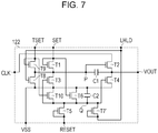
- the seventh thin-film transistor T7 whose gate is connected to the fifth input unit LHLD, source or gate is connected to the third input unit VSS, and the other of the source and the drain is connected to the output unit VOUT is used in the third circuit.
- a seventh thin-film transistor T7' may be used instead of the seventh thin-film transistor T7 illustrated in Fig. 1B .
- a gate and either a source or a drain of the seventh thin-film transistor T7' are connected to the fifth input unit LHLD, and the other of the source and the drain is connected to the second node Q.
- the fourth thin-film transistor T4 belongs not only to the second circuit but also to the third circuit.
- voltage equal to or higher than Vth continues to be supplied to the gate of the third thin-film transistor T3, and accordingly the non-conducting voltage V SS is continued to be supplied to the first node P by the third thin-film transistor T3.
- the third thin-film transistor T3 belongs not only to the second circuit but also to the third circuit.
- Fig. 5A illustrates a schematic equivalent circuit of the detection apparatus
- Fig. 5B illustrates a schematic equivalent circuit of a unit circuit provided in a driving circuit unit of the detection apparatus.
- the same components as those described in the first exemplary embodiment are given the same reference numerals, and therefore detailed description thereof is omitted.
- a driving circuit unit 120' includes a plurality of unit circuit groups, each including a plurality of unit circuits 121.
- X unit circuit groups each including three stages of unit circuits are provided.
- a control unit 150' is configured to be able to independently supply control signals ⁇ LH1 to ⁇ LHx to the plurality of unit circuit groups, respectively. Therefore, it is possible to independently control the supply of the non-conducting voltage V SS to the driving wire 160 in each unit circuit group.
- the control unit 150' is configured to be able to independently supply a start signal ⁇ ST1 and selection signals ⁇ ST2 to ⁇ STx to the plurality of unit circuit groups, respectively.
- a unit circuit 122 illustrated in Fig. 5B is used as an initial-stage unit circuit in each unit circuit group except for the first-stage unit circuit 121.
- the unit circuit 122 further includes a sixth input unit TSET and a fourth circuit in addition to the components of the unit circuit 121.
- the fourth circuit is a circuit that causes the first circuit to supply the conducting voltage V DD to the driving wire 160 in accordance with any of the selection signals ⁇ ST2 to ⁇ STx, and includes a ninth thin-film transistor T9 and a tenth thin-film transistor T10.
- the ninth thin-film transistor T9 is connected between the sixth input unit TSET and the other end of the first capacitor C1 in series with the first capacitor C1. Either a source or a drain and a gate of the ninth thin-film transistor T9 are connected to the sixth input unit TSET, and the other of the source and the drain of the ninth thin-film transistor T9 is connected to the first node P.
- the tenth thin-film transistor T10 is provided parallel to the second capacitor C2 and the sixth thin-film transistor T6.
- a gate of the tenth thin-film transistor T10 is connected to the sixth input unit TSET, either a source or a drain of the tenth thin-film transistor T10 is connected to the third input unit VSS, and the other of the source and the drain of the tenth thin-film transistor T10 is connected to the second node Q.
- the voltage V SS of the start signal ⁇ ST1 is supplied to the first input unit SET of the first-stage unit circuit 121 and the voltage V SS of the clock signal ⁇ CL1 is supplied to the second input unit CLK from the control unit 150'.
- the voltage V DD of the control signal ⁇ LH1 is supplied to the fifth input units LHLD of all the unit circuits 121 in the first group from the control unit 150'.
- the voltage V SS of the selection signal ⁇ STx is supplied to the first input unit SET of an (m - 2)th unit circuit 121, which is the initial-stage unit circuit 121 in the X-th unit circuit group, and the voltage V SS of the clock signal ⁇ CL1 is supplied to the second input unit CLK of the (m - 2)th unit circuit 121 from the control unit 150'.
- the voltage V DD of the control signal ⁇ LHx is supplied to the fifth input units LHLD of all the unit circuits 121 and the unit circuit 122 in the X-th unit circuit group from the control unit 150'.
- the potential of the output units VOUT of all the unit circuits 121 and the unit circuit 122 in the first and the X-th unit circuit groups becomes V SS .
- the control signals ⁇ LH1 and ⁇ LHx are kept at V DD until a time t5, which will be described later, and the potential of the output units VOUT of all the unit circuits 121 and the unit circuit 122 in the first and the X-th unit circuit groups is kept at V SS until the time t5.
- the output units VOUT of the unit circuits 121 and the unit circuit 122 in the unit circuit groups (the first and the X-th unit circuit groups) among the plurality of unit circuit groups except for unit circuit groups including the unit circuits 121 connected to the plurality of driving wires 160 to which the conducting voltage is to be selectively supplied are kept at the non-conducting voltage V SS .
- the voltage V SS of the output signal Vg3 of the third-stage unit circuit 121 is supplied to the first input unit SET of the fourth-stage unit circuit 122, which is the initial-stage unit circuit in the second unit circuit group, the voltage V DD of the clock signal ⁇ CL2 is supplied to the second input unit CLK of the fourth-stage unit circuit 122, and the voltage V SS of the control signal ⁇ LH is supplied to the fifth input unit LHLD of the fourth-stage unit circuit 122 from the control unit 150'.
- the voltage V SS is supplied to the third input unit VSS of the fourth-stage unit circuit 122 from the power supply unit 140, and the voltage V SS of an output signal Vg5 of a fifth-stage unit circuit 121 is supplied to the fourth input unit RESET of the fourth-stage unit circuit 122. Furthermore, the voltage V DD of the selection signal ⁇ ST2 is supplied to the sixth input unit TSET of the fourth-stage unit circuit 122. Therefore, in the fourth-stage unit circuit 122, the ninth thin-film transistor T9 and the tenth thin-film transistor T10 become conductive. In the fourth-stage unit circuit 122, the first thin-film transistor T1 to the eighth thin-film transistor T8 become non-conductive.
- the fourth-stage unit circuit 122 As a result, in the fourth-stage unit circuit 122, the potential of the first node P becomes
- the voltage V SS of the output signal Vg3 of the third-stage unit circuit 121 is supplied to the first input unit SET of the fourth-stage unit circuit 122, the voltage V DD of the clock signal ⁇ CL2 is supplied to the second input unit CLK of the fourth-stage unit circuit 122, and the voltage V SS of the control signal ⁇ LH2 is supplied to the fifth input unit LHLD of the fourth-stage unit circuit 122 from the control unit 150'.
- the voltage V SS is supplied to the third input unit VSS of the fourth-stage unit circuit 122 from the power supply unit 140, and the voltage V SS of the output signal Vg2 of the second-stage unit circuit 121 is supplied to the fourth input unit RESET.
- the voltage V SS of the selection signal ⁇ ST2 is supplied to the sixth input unit TSET from the control unit 150'. Therefore, in the fourth-stage unit circuit 122, the thin-film transistors other than the second thin-film transistor T2 become non-conductive. At this time, since the other of the source and the drain and the gate of the second thin-film transistor T2 are connected to each other through the first capacitor C1, the potential of the first node P becomes
- the voltage V DD is supplied to the driving wire 160 in the fourth row from the fourth-stage unit circuit 122 as an output signal Vg4, and accordingly the plurality of switch elements 112 in the fourth row become conductive. Therefore, electrical signals according to the electric charge of the plurality of conversion elements 111 in the fourth row are output parallel to one another to the plurality of signal wires 170, respectively, arranged in the row direction.
- the voltage V DD of the output signal Vg4 of the fourth-stage unit circuit 122 is supplied to the first input unit SET of the fifth-stage unit circuit 121
- the voltage V SS of the clock signal ⁇ CL1 is supplied to the second input unit CLK of the fifth-stage unit circuit 121
- the voltage V SS of the control signal ⁇ LH2 is supplied to the fifth input unit LHLD of the fifth-stage circuit unit 121 from the control unit 150'.
- the voltage V SS is supplied to the third input unit VSS of the fifth-stage unit circuit 121 from the power supply unit 140
- the voltage V SS of an output signal Vg6 is supplied to the fourth input unit RESET of the fifth-stage unit circuit 121.
- the potential of the first node P becomes
- the potential of the second node Q becomes V SS
- the second thin-film transistor T2 becomes conductive
- the potential of the output unit VOUT becomes V SS .
- the voltage of the output signal Vg3 of the third-stage unit circuit 121 is supplied to the first input unit SET of the fourth-stage unit circuit 122, the voltage V SS of the clock signal ⁇ CL2 is supplied to the second input unit CLK of the fourth-stage unit circuit 122, and the voltage V SS of the control signal ⁇ LH2 is supplied to the fifth input unit LHLD from the control unit 150'.
- the voltage V SS is supplied to the third input unit VSS of the fourth-stage unit circuit 122 from the power supply unit 140, and the voltage V DD of the output signal Vg2 of the fifth-stage unit circuit 121, which will be described later, is supplied to the fourth input unit RESET of the fourth-stage unit circuit 122.
- the voltage V SS of the selection signal ⁇ ST2 is supplied to the sixth input unit TSET of the fourth-stage unit circuit 122 from the control unit 150'. Therefore, in the fourth-stage unit circuit 122, the first thin-film transistor T1 and the sixth thin-film transistor T6 to the tenth thin-film transistor T10 are non-conductive. In the fourth-stage unit circuit 122, the fifth thin-film transistor T5 becomes conductive. Therefore, in the fourth-stage unit circuit 122, the potential of the first node P becomes V SS , and the potential of the second node Q becomes
- the second thin-film transistor T2 becomes non-conductive
- the third thin-film transistor T3 and the fourth thin-film transistor T4 become conductive
- the potential of the output unit VOUT becomes V SS .
- the voltage V SS of the output signal Vg4 of the first-stage unit circuit 121 is supplied to the first input unit SET of the fifth-stage unit circuit 121
- the voltage V DD of the clock signal ⁇ CL1 is supplied to the second input unit CLK of the fifth-stage unit circuit 121
- the voltage V SS of the control signal ⁇ LH2 is supplied to the fifth input unit LHLD of the fifth-stage unit circuit 121 from the control unit 150'.
- the voltage V SS is supplied to the third input unit VSS of the fifth-stage unit circuit 121 from the power supply unit 140, and the voltage V SS of the output signal Vg6 of the sixth-stage unit circuit 121 is supplied to the fourth input unit RESET of the fifth-stage unit circuit 121. Therefore, as with the fourth-stage unit circuit 122 at the time t2, in the fifth-stage unit circuit 121, the potential of the first node P becomes
- the fifth-stage (next stage) unit circuit 121 executes the same operation as the fourth-stage (previous stage) unit circuit 122 half the period (t3 - t2) of the clock signal later than the fourth-stage (previous stage) unit circuit 122 using the voltage V DD of the output signal Vg4 of the fourth-stage (previous stage) unit circuit 122 as a trigger.
- Such an operation is sequentially executed up to an (m - 3)th unit circuit 121, and the conducting voltage V DD is sequentially supplied to the plurality of driving wires 160, which are arranged in the column direction, up to an (m - 3)th driving wire 160 from the driving circuit unit 120.
- the voltage V DD of the control signal ⁇ LH2 is supplied to the fifth input units LHLD of all the unit circuits 121 and the unit circuit 122 in the second unit circuit group from the control unit 150'. Therefore, the potential of the output units VOUT of the all the unit circuits 121 and the unit circuit 122 in the second unit circuit group becomes V SS .
- the control signal ⁇ LH2 is kept at V DD until the time t5, and the potential of the output units VOUT of all the unit circuits 121 and the unit circuit 122 in the second unit circuit group is kept at V SS until the time t5.
- the operation at the time t5 and later is the same as that according to the first exemplary embodiment, except that the voltage V SS of the control signals ⁇ LH2 to ⁇ LHx is supplied to the fifth input units LHLD of the initial-stage unit circuits 122, respectively, other than the initial-stage unit circuit 121 in the first unit circuit group from the control unit 150'. Therefore, detailed description of the operation is omitted.
- unit circuit groups selected from among the plurality of unit circuit groups it is possible to operate unit circuit groups selected from among the plurality of unit circuit groups. Furthermore, even when unit circuit groups are operated by selecting the unit circuit groups from among the plurality of unit circuit groups, it is possible to provide a detection apparatus that can suppress a decrease in the S/N ratio caused by variation in the potential of the driving wires 160.
- the seventh thin-film transistor T7 whose gate is connected to the fifth input unit LHLD, source or drain is connected to the third input unit VSS, and the other of the source and the drain is connected to the output unit VOUT is used in the third circuit.
- a seventh thin-film transistor T7' may be used as illustrated in Fig. 7 .
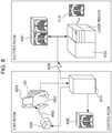
- An X-ray 6060 generated by an X-ray tube 6050 which is a radiation source, propagates through a chest 6062 of a patient or subject 6061 and is incident on each conversion element of a conversion unit included in a radiation detection apparatus.
- the incident X-ray includes information regarding the inside of the chest 6062 of the patient 6061.
- the radiation is converted into electric charge by the conversion unit in accordance with the incident X-ray to obtain electrical information.
- This information is converted into digital data and then subjected to image processing in an image processor 6070.
- the information after the image processing can be observed on a display 6080, which serves as a display unit in a control room.
- this information can be transferred to a distant place by a transmission process unit such as a telephone network 6090 to display the information on a display 6081, which serves as a display unit, or to save the information to a recording medium such as an optical disk in a doctor's room or the like located in the distance place, and can be seen by the doctor in the distant place.
- the information can also be recorded on a film 6110, which serves as a recording medium, by a film processor 6100, which serves as a recording unit.
Landscapes
- Engineering & Computer Science (AREA)
- Physics & Mathematics (AREA)
- Power Engineering (AREA)
- Computer Hardware Design (AREA)
- Microelectronics & Electronic Packaging (AREA)
- Electromagnetism (AREA)
- Condensed Matter Physics & Semiconductors (AREA)
- General Physics & Mathematics (AREA)
- Multimedia (AREA)
- Signal Processing (AREA)
- Chemical & Material Sciences (AREA)
- Health & Medical Sciences (AREA)
- Toxicology (AREA)
- Materials Engineering (AREA)
- Nanotechnology (AREA)
- Solid State Image Pick-Up Elements (AREA)
- Control Of Indicators Other Than Cathode Ray Tubes (AREA)
- Measurement Of Radiation (AREA)
- Apparatus For Radiation Diagnosis (AREA)
- Transforming Light Signals Into Electric Signals (AREA)
Applications Claiming Priority (1)
| Application Number | Priority Date | Filing Date | Title |
|---|---|---|---|
| JP2011159011A JP5847472B2 (ja) | 2011-07-20 | 2011-07-20 | 検出装置及び検出システム |
Publications (3)
| Publication Number | Publication Date |
|---|---|
| EP2549299A2 EP2549299A2 (en) | 2013-01-23 |
| EP2549299A3 EP2549299A3 (en) | 2015-04-01 |
| EP2549299B1 true EP2549299B1 (en) | 2019-10-30 |
Family
ID=46980707
Family Applications (1)
| Application Number | Title | Priority Date | Filing Date |
|---|---|---|---|
| EP12173101.2A Active EP2549299B1 (en) | 2011-07-20 | 2012-06-22 | Radiation detection apparatus and detection system including same |
Country Status (4)
| Country | Link |
|---|---|
| US (1) | US8680478B2 (ja) |
| EP (1) | EP2549299B1 (ja) |
| JP (1) | JP5847472B2 (ja) |
| CN (1) | CN102885632B (ja) |
Families Citing this family (11)
| Publication number | Priority date | Publication date | Assignee | Title |
|---|---|---|---|---|
| JP2014192320A (ja) * | 2013-03-27 | 2014-10-06 | Sony Corp | 撮像装置および撮像表示システム |
| FR3013546B1 (fr) * | 2013-11-15 | 2017-05-19 | Trixell | Mise en commun de deux colonnes de pixels d'un detecteur d'images |
| JP6339853B2 (ja) * | 2014-05-01 | 2018-06-06 | キヤノン株式会社 | 放射線撮像装置および放射線撮像システム |
| KR102509203B1 (ko) * | 2014-08-29 | 2023-03-14 | 가부시키가이샤 한도오따이 에네루기 켄큐쇼 | 촬상 장치 및 전자 기기 |
| US10163948B2 (en) * | 2015-07-23 | 2018-12-25 | Semiconductor Energy Laboratory Co., Ltd. | Imaging device and electronic device |
| US10356027B2 (en) * | 2016-10-03 | 2019-07-16 | HYP3R Inc | Location resolution of social media posts |
| US10527728B2 (en) * | 2017-01-27 | 2020-01-07 | Samsung Electronics Co., Ltd | Apparatus and method for range measurement |
| KR102462071B1 (ko) * | 2017-12-27 | 2022-11-01 | 엘지디스플레이 주식회사 | 시프트 레지스터, 게이트 구동 회로, 엑스선 탐지 패널 및 엑스선 탐지 장치 |
| JP7088686B2 (ja) * | 2018-02-15 | 2022-06-21 | Tianma Japan株式会社 | イメージセンサ及びイメージセンサの駆動方法 |
| CN110853591A (zh) * | 2019-11-11 | 2020-02-28 | 福建华佳彩有限公司 | 一种gip驱动电路及其控制方法 |
| KR20230047392A (ko) * | 2020-08-03 | 2023-04-07 | 가부시키가이샤 한도오따이 에네루기 켄큐쇼 | 반도체 장치 및 전자 기기 |
Citations (1)
| Publication number | Priority date | Publication date | Assignee | Title |
|---|---|---|---|---|
| WO2010113809A1 (ja) * | 2009-04-01 | 2010-10-07 | 浜松ホトニクス株式会社 | 固体撮像素子及びその製造方法、放射線撮像装置及びその製造方法、並びに固体撮像素子の検査方法 |
Family Cites Families (12)
| Publication number | Priority date | Publication date | Assignee | Title |
|---|---|---|---|---|
| JPS6449381A (en) * | 1987-08-20 | 1989-02-23 | Fuji Photo Film Co Ltd | Solid-state image pickup device |
| JPH04114395A (ja) * | 1990-09-05 | 1992-04-15 | Nec Corp | 半導体記憶回路 |
| JPH09163244A (ja) * | 1995-12-05 | 1997-06-20 | Olympus Optical Co Ltd | 固体撮像装置 |
| JP2001056382A (ja) * | 1999-06-07 | 2001-02-27 | Toshiba Corp | 放射線検出器及び放射線診断装置 |
| JP2001273785A (ja) * | 2000-03-29 | 2001-10-05 | Casio Comput Co Ltd | シフトレジスタ及び電子装置 |
| JP4670834B2 (ja) * | 2007-05-21 | 2011-04-13 | エプソンイメージングデバイス株式会社 | 電気光学装置、電気光学装置の駆動回路及び電気機器 |
| JP4991459B2 (ja) * | 2007-09-07 | 2012-08-01 | キヤノン株式会社 | 撮像装置及び放射線撮像システム |
| JP5188221B2 (ja) * | 2008-03-14 | 2013-04-24 | キヤノン株式会社 | 固体撮像装置 |
| JP5392533B2 (ja) * | 2008-10-10 | 2014-01-22 | ソニー株式会社 | 固体撮像素子、光学装置、信号処理装置及び信号処理システム |
| JP2011015158A (ja) * | 2009-07-01 | 2011-01-20 | Toshiba Corp | 固体撮像装置 |
| JP5436121B2 (ja) * | 2009-09-28 | 2014-03-05 | キヤノン株式会社 | 撮像装置および放射線撮像システム |
| US8054935B2 (en) * | 2009-11-13 | 2011-11-08 | Au Optronics Corporation | Shift register with low power consumption |
-
2011
- 2011-07-20 JP JP2011159011A patent/JP5847472B2/ja active Active
-
2012
- 2012-06-22 EP EP12173101.2A patent/EP2549299B1/en active Active
- 2012-07-09 US US13/544,105 patent/US8680478B2/en active Active
- 2012-07-19 CN CN201210250693.0A patent/CN102885632B/zh active Active
Patent Citations (1)
| Publication number | Priority date | Publication date | Assignee | Title |
|---|---|---|---|---|
| WO2010113809A1 (ja) * | 2009-04-01 | 2010-10-07 | 浜松ホトニクス株式会社 | 固体撮像素子及びその製造方法、放射線撮像装置及びその製造方法、並びに固体撮像素子の検査方法 |
Also Published As
| Publication number | Publication date |
|---|---|
| JP2013026780A (ja) | 2013-02-04 |
| JP5847472B2 (ja) | 2016-01-20 |
| US8680478B2 (en) | 2014-03-25 |
| US20130020494A1 (en) | 2013-01-24 |
| CN102885632B (zh) | 2014-09-24 |
| EP2549299A3 (en) | 2015-04-01 |
| EP2549299A2 (en) | 2013-01-23 |
| CN102885632A (zh) | 2013-01-23 |
Similar Documents
| Publication | Publication Date | Title |
|---|---|---|
| EP2549299B1 (en) | Radiation detection apparatus and detection system including same | |
| JP5173234B2 (ja) | 放射線撮像装置及び放射線撮像システム | |
| JP5963551B2 (ja) | アクティブマトリクスパネル、検出装置、及び、検出システム | |
| US7205568B2 (en) | Solid state image pickup apparatus and radiation image pickup apparatus | |
| US8878972B2 (en) | Imaging apparatus, radiation imaging system, and method for driving imaging apparatus | |
| CN105282462B (zh) | 图像传感器及其驱动方法 | |
| US20100148080A1 (en) | Imaging apparatus and radiation imaging system | |
| US20130342514A1 (en) | Detection apparatus, detection system, and detection apparatus drive method | |
| US8822939B2 (en) | Matrix substrate, detection device, detection system, and method for driving detection device | |
| US20120080605A1 (en) | Detection apparatus and radiation detection system | |
| US9018590B2 (en) | Device for addressing lines of a control circuit for an active detection matrix | |
| US8405039B2 (en) | Detection apparatus and radiation detection system | |
| US9564461B2 (en) | Radiation image-pickup device and radiation image-pickup display system | |
| US20130187837A1 (en) | Matrix substrate, detecting device, and detecting system | |
| CN109087925B (zh) | 阵列基板、x射线平板探测器及x射线探测方法 | |
| US20130075621A1 (en) | Radiation detection apparatus and detection system including same | |
| US9536921B2 (en) | Radiation image-pickup device and radiation image-pickup display system | |
| JP6138319B2 (ja) | 検出装置、及び、検出システム | |
| JP2013033945A (ja) | 検出装置及び検出システム |
Legal Events
| Date | Code | Title | Description |
|---|---|---|---|
| PUAI | Public reference made under article 153(3) epc to a published international application that has entered the european phase |
Free format text: ORIGINAL CODE: 0009012 |
|
| AK | Designated contracting states |
Kind code of ref document: A2 Designated state(s): AL AT BE BG CH CY CZ DE DK EE ES FI FR GB GR HR HU IE IS IT LI LT LU LV MC MK MT NL NO PL PT RO RS SE SI SK SM TR |
|
| AX | Request for extension of the european patent |
Extension state: BA ME |
|
| PUAL | Search report despatched |
Free format text: ORIGINAL CODE: 0009013 |
|
| AK | Designated contracting states |
Kind code of ref document: A3 Designated state(s): AL AT BE BG CH CY CZ DE DK EE ES FI FR GB GR HR HU IE IS IT LI LT LU LV MC MK MT NL NO PL PT RO RS SE SI SK SM TR |
|
| AX | Request for extension of the european patent |
Extension state: BA ME |
|
| RIC1 | Information provided on ipc code assigned before grant |
Ipc: G01T 1/24 20060101AFI20150223BHEP |
|
| 17P | Request for examination filed |
Effective date: 20151001 |
|
| RBV | Designated contracting states (corrected) |
Designated state(s): AL AT BE BG CH CY CZ DE DK EE ES FI FR GB GR HR HU IE IS IT LI LT LU LV MC MK MT NL NO PL PT RO RS SE SI SK SM TR |
|
| STAA | Information on the status of an ep patent application or granted ep patent |
Free format text: STATUS: EXAMINATION IS IN PROGRESS |
|
| 17Q | First examination report despatched |
Effective date: 20171204 |
|
| GRAP | Despatch of communication of intention to grant a patent |
Free format text: ORIGINAL CODE: EPIDOSNIGR1 |
|
| STAA | Information on the status of an ep patent application or granted ep patent |
Free format text: STATUS: GRANT OF PATENT IS INTENDED |
|
| INTG | Intention to grant announced |
Effective date: 20190510 |
|
| RAP1 | Party data changed (applicant data changed or rights of an application transferred) |
Owner name: CANON KABUSHIKI KAISHA |
|
| RIN1 | Information on inventor provided before grant (corrected) |
Inventor name: FUJIYOSHI, KENTARO Inventor name: MOCHIZUKI, CHIORI Inventor name: YOKOYAMA, KEIGO Inventor name: WATANABE, MINORU Inventor name: OFUJI, MASATO Inventor name: WAYAMA, HIROSHI Inventor name: KAWANABE, JUN |
|
| GRAS | Grant fee paid |
Free format text: ORIGINAL CODE: EPIDOSNIGR3 |
|
| GRAA | (expected) grant |
Free format text: ORIGINAL CODE: 0009210 |
|
| STAA | Information on the status of an ep patent application or granted ep patent |
Free format text: STATUS: THE PATENT HAS BEEN GRANTED |
|
| AK | Designated contracting states |
Kind code of ref document: B1 Designated state(s): AL AT BE BG CH CY CZ DE DK EE ES FI FR GB GR HR HU IE IS IT LI LT LU LV MC MK MT NL NO PL PT RO RS SE SI SK SM TR |
|
| REG | Reference to a national code |
Ref country code: GB Ref legal event code: FG4D |
|
| REG | Reference to a national code |
Ref country code: CH Ref legal event code: EP |
|
| REG | Reference to a national code |
Ref country code: AT Ref legal event code: REF Ref document number: 1196752 Country of ref document: AT Kind code of ref document: T Effective date: 20191115 |
|
| REG | Reference to a national code |
Ref country code: DE Ref legal event code: R096 Ref document number: 602012065207 Country of ref document: DE |
|
| REG | Reference to a national code |
Ref country code: IE Ref legal event code: FG4D |
|
| REG | Reference to a national code |
Ref country code: LT Ref legal event code: MG4D |
|
| PG25 | Lapsed in a contracting state [announced via postgrant information from national office to epo] |
Ref country code: NO Free format text: LAPSE BECAUSE OF FAILURE TO SUBMIT A TRANSLATION OF THE DESCRIPTION OR TO PAY THE FEE WITHIN THE PRESCRIBED TIME-LIMIT Effective date: 20200130 Ref country code: PT Free format text: LAPSE BECAUSE OF FAILURE TO SUBMIT A TRANSLATION OF THE DESCRIPTION OR TO PAY THE FEE WITHIN THE PRESCRIBED TIME-LIMIT Effective date: 20200302 Ref country code: FI Free format text: LAPSE BECAUSE OF FAILURE TO SUBMIT A TRANSLATION OF THE DESCRIPTION OR TO PAY THE FEE WITHIN THE PRESCRIBED TIME-LIMIT Effective date: 20191030 Ref country code: BG Free format text: LAPSE BECAUSE OF FAILURE TO SUBMIT A TRANSLATION OF THE DESCRIPTION OR TO PAY THE FEE WITHIN THE PRESCRIBED TIME-LIMIT Effective date: 20200130 Ref country code: LV Free format text: LAPSE BECAUSE OF FAILURE TO SUBMIT A TRANSLATION OF THE DESCRIPTION OR TO PAY THE FEE WITHIN THE PRESCRIBED TIME-LIMIT Effective date: 20191030 Ref country code: SE Free format text: LAPSE BECAUSE OF FAILURE TO SUBMIT A TRANSLATION OF THE DESCRIPTION OR TO PAY THE FEE WITHIN THE PRESCRIBED TIME-LIMIT Effective date: 20191030 Ref country code: PL Free format text: LAPSE BECAUSE OF FAILURE TO SUBMIT A TRANSLATION OF THE DESCRIPTION OR TO PAY THE FEE WITHIN THE PRESCRIBED TIME-LIMIT Effective date: 20191030 Ref country code: GR Free format text: LAPSE BECAUSE OF FAILURE TO SUBMIT A TRANSLATION OF THE DESCRIPTION OR TO PAY THE FEE WITHIN THE PRESCRIBED TIME-LIMIT Effective date: 20200131 Ref country code: ES Free format text: LAPSE BECAUSE OF FAILURE TO SUBMIT A TRANSLATION OF THE DESCRIPTION OR TO PAY THE FEE WITHIN THE PRESCRIBED TIME-LIMIT Effective date: 20191030 Ref country code: LT Free format text: LAPSE BECAUSE OF FAILURE TO SUBMIT A TRANSLATION OF THE DESCRIPTION OR TO PAY THE FEE WITHIN THE PRESCRIBED TIME-LIMIT Effective date: 20191030 Ref country code: NL Free format text: LAPSE BECAUSE OF FAILURE TO SUBMIT A TRANSLATION OF THE DESCRIPTION OR TO PAY THE FEE WITHIN THE PRESCRIBED TIME-LIMIT Effective date: 20191030 |
|
| REG | Reference to a national code |
Ref country code: NL Ref legal event code: MP Effective date: 20191030 |
|
| PG25 | Lapsed in a contracting state [announced via postgrant information from national office to epo] |
Ref country code: RS Free format text: LAPSE BECAUSE OF FAILURE TO SUBMIT A TRANSLATION OF THE DESCRIPTION OR TO PAY THE FEE WITHIN THE PRESCRIBED TIME-LIMIT Effective date: 20191030 Ref country code: HR Free format text: LAPSE BECAUSE OF FAILURE TO SUBMIT A TRANSLATION OF THE DESCRIPTION OR TO PAY THE FEE WITHIN THE PRESCRIBED TIME-LIMIT Effective date: 20191030 Ref country code: IS Free format text: LAPSE BECAUSE OF FAILURE TO SUBMIT A TRANSLATION OF THE DESCRIPTION OR TO PAY THE FEE WITHIN THE PRESCRIBED TIME-LIMIT Effective date: 20200229 |
|
| PG25 | Lapsed in a contracting state [announced via postgrant information from national office to epo] |
Ref country code: AL Free format text: LAPSE BECAUSE OF FAILURE TO SUBMIT A TRANSLATION OF THE DESCRIPTION OR TO PAY THE FEE WITHIN THE PRESCRIBED TIME-LIMIT Effective date: 20191030 |
|
| PG25 | Lapsed in a contracting state [announced via postgrant information from national office to epo] |
Ref country code: DK Free format text: LAPSE BECAUSE OF FAILURE TO SUBMIT A TRANSLATION OF THE DESCRIPTION OR TO PAY THE FEE WITHIN THE PRESCRIBED TIME-LIMIT Effective date: 20191030 Ref country code: EE Free format text: LAPSE BECAUSE OF FAILURE TO SUBMIT A TRANSLATION OF THE DESCRIPTION OR TO PAY THE FEE WITHIN THE PRESCRIBED TIME-LIMIT Effective date: 20191030 Ref country code: RO Free format text: LAPSE BECAUSE OF FAILURE TO SUBMIT A TRANSLATION OF THE DESCRIPTION OR TO PAY THE FEE WITHIN THE PRESCRIBED TIME-LIMIT Effective date: 20191030 Ref country code: CZ Free format text: LAPSE BECAUSE OF FAILURE TO SUBMIT A TRANSLATION OF THE DESCRIPTION OR TO PAY THE FEE WITHIN THE PRESCRIBED TIME-LIMIT Effective date: 20191030 |
|
| REG | Reference to a national code |
Ref country code: DE Ref legal event code: R097 Ref document number: 602012065207 Country of ref document: DE |
|
| REG | Reference to a national code |
Ref country code: AT Ref legal event code: MK05 Ref document number: 1196752 Country of ref document: AT Kind code of ref document: T Effective date: 20191030 |
|
| PG25 | Lapsed in a contracting state [announced via postgrant information from national office to epo] |
Ref country code: SM Free format text: LAPSE BECAUSE OF FAILURE TO SUBMIT A TRANSLATION OF THE DESCRIPTION OR TO PAY THE FEE WITHIN THE PRESCRIBED TIME-LIMIT Effective date: 20191030 Ref country code: IT Free format text: LAPSE BECAUSE OF FAILURE TO SUBMIT A TRANSLATION OF THE DESCRIPTION OR TO PAY THE FEE WITHIN THE PRESCRIBED TIME-LIMIT Effective date: 20191030 Ref country code: SK Free format text: LAPSE BECAUSE OF FAILURE TO SUBMIT A TRANSLATION OF THE DESCRIPTION OR TO PAY THE FEE WITHIN THE PRESCRIBED TIME-LIMIT Effective date: 20191030 |
|
| PLBE | No opposition filed within time limit |
Free format text: ORIGINAL CODE: 0009261 |
|
| STAA | Information on the status of an ep patent application or granted ep patent |
Free format text: STATUS: NO OPPOSITION FILED WITHIN TIME LIMIT |
|
| 26N | No opposition filed |
Effective date: 20200731 |
|
| PG25 | Lapsed in a contracting state [announced via postgrant information from national office to epo] |
Ref country code: AT Free format text: LAPSE BECAUSE OF FAILURE TO SUBMIT A TRANSLATION OF THE DESCRIPTION OR TO PAY THE FEE WITHIN THE PRESCRIBED TIME-LIMIT Effective date: 20191030 Ref country code: SI Free format text: LAPSE BECAUSE OF FAILURE TO SUBMIT A TRANSLATION OF THE DESCRIPTION OR TO PAY THE FEE WITHIN THE PRESCRIBED TIME-LIMIT Effective date: 20191030 |
|
| PG25 | Lapsed in a contracting state [announced via postgrant information from national office to epo] |
Ref country code: MC Free format text: LAPSE BECAUSE OF FAILURE TO SUBMIT A TRANSLATION OF THE DESCRIPTION OR TO PAY THE FEE WITHIN THE PRESCRIBED TIME-LIMIT Effective date: 20191030 |
|
| REG | Reference to a national code |
Ref country code: CH Ref legal event code: PL |
|
| GBPC | Gb: european patent ceased through non-payment of renewal fee |
Effective date: 20200622 |
|
| PG25 | Lapsed in a contracting state [announced via postgrant information from national office to epo] |
Ref country code: LU Free format text: LAPSE BECAUSE OF NON-PAYMENT OF DUE FEES Effective date: 20200622 |
|
| REG | Reference to a national code |
Ref country code: BE Ref legal event code: MM Effective date: 20200630 |
|
| PG25 | Lapsed in a contracting state [announced via postgrant information from national office to epo] |
Ref country code: CH Free format text: LAPSE BECAUSE OF NON-PAYMENT OF DUE FEES Effective date: 20200630 Ref country code: IE Free format text: LAPSE BECAUSE OF NON-PAYMENT OF DUE FEES Effective date: 20200622 Ref country code: LI Free format text: LAPSE BECAUSE OF NON-PAYMENT OF DUE FEES Effective date: 20200630 Ref country code: FR Free format text: LAPSE BECAUSE OF NON-PAYMENT OF DUE FEES Effective date: 20200630 Ref country code: GB Free format text: LAPSE BECAUSE OF NON-PAYMENT OF DUE FEES Effective date: 20200622 |
|
| PG25 | Lapsed in a contracting state [announced via postgrant information from national office to epo] |
Ref country code: BE Free format text: LAPSE BECAUSE OF NON-PAYMENT OF DUE FEES Effective date: 20200630 |
|
| PG25 | Lapsed in a contracting state [announced via postgrant information from national office to epo] |
Ref country code: TR Free format text: LAPSE BECAUSE OF FAILURE TO SUBMIT A TRANSLATION OF THE DESCRIPTION OR TO PAY THE FEE WITHIN THE PRESCRIBED TIME-LIMIT Effective date: 20191030 Ref country code: MT Free format text: LAPSE BECAUSE OF FAILURE TO SUBMIT A TRANSLATION OF THE DESCRIPTION OR TO PAY THE FEE WITHIN THE PRESCRIBED TIME-LIMIT Effective date: 20191030 Ref country code: CY Free format text: LAPSE BECAUSE OF FAILURE TO SUBMIT A TRANSLATION OF THE DESCRIPTION OR TO PAY THE FEE WITHIN THE PRESCRIBED TIME-LIMIT Effective date: 20191030 |
|
| PG25 | Lapsed in a contracting state [announced via postgrant information from national office to epo] |
Ref country code: MK Free format text: LAPSE BECAUSE OF FAILURE TO SUBMIT A TRANSLATION OF THE DESCRIPTION OR TO PAY THE FEE WITHIN THE PRESCRIBED TIME-LIMIT Effective date: 20191030 |
|
| PGFP | Annual fee paid to national office [announced via postgrant information from national office to epo] |
Ref country code: DE Payment date: 20230523 Year of fee payment: 12 |