EP2546732A2 - Eingabegerät - Google Patents
Eingabegerät Download PDFInfo
- Publication number
- EP2546732A2 EP2546732A2 EP12175979A EP12175979A EP2546732A2 EP 2546732 A2 EP2546732 A2 EP 2546732A2 EP 12175979 A EP12175979 A EP 12175979A EP 12175979 A EP12175979 A EP 12175979A EP 2546732 A2 EP2546732 A2 EP 2546732A2
- Authority
- EP
- European Patent Office
- Prior art keywords
- magnetic field
- shielding layer
- magnetic
- input device
- geo
- Prior art date
- Legal status (The legal status is an assumption and is not a legal conclusion. Google has not performed a legal analysis and makes no representation as to the accuracy of the status listed.)
- Ceased
Links
Images


Classifications
-
- G—PHYSICS
- G06—COMPUTING OR CALCULATING; COUNTING
- G06F—ELECTRIC DIGITAL DATA PROCESSING
- G06F3/00—Input arrangements for transferring data to be processed into a form capable of being handled by the computer; Output arrangements for transferring data from processing unit to output unit, e.g. interface arrangements
- G06F3/01—Input arrangements or combined input and output arrangements for interaction between user and computer
- G06F3/03—Arrangements for converting the position or the displacement of a member into a coded form
- G06F3/033—Pointing devices displaced or positioned by the user, e.g. mice, trackballs, pens or joysticks; Accessories therefor
- G06F3/0354—Pointing devices displaced or positioned by the user, e.g. mice, trackballs, pens or joysticks; Accessories therefor with detection of two-dimensional [2D] relative movements between the device, or an operating part thereof, and a plane or surface, e.g. 2D mice, trackballs, pens or pucks
- G06F3/03545—Pens or stylus
-
- G—PHYSICS
- G01—MEASURING; TESTING
- G01V—GEOPHYSICS; GRAVITATIONAL MEASUREMENTS; DETECTING MASSES OR OBJECTS; TAGS
- G01V3/00—Electric or magnetic prospecting or detecting; Measuring magnetic field characteristics of the earth, e.g. declination, deviation
- G01V3/40—Electric or magnetic prospecting or detecting; Measuring magnetic field characteristics of the earth, e.g. declination, deviation specially adapted for measuring magnetic field characteristics of the earth
-
- G—PHYSICS
- G06—COMPUTING OR CALCULATING; COUNTING
- G06F—ELECTRIC DIGITAL DATA PROCESSING
- G06F3/00—Input arrangements for transferring data to be processed into a form capable of being handled by the computer; Output arrangements for transferring data from processing unit to output unit, e.g. interface arrangements
- G06F3/01—Input arrangements or combined input and output arrangements for interaction between user and computer
- G06F3/03—Arrangements for converting the position or the displacement of a member into a coded form
- G06F3/041—Digitisers, e.g. for touch screens or touch pads, characterised by the transducing means
- G06F3/046—Digitisers, e.g. for touch screens or touch pads, characterised by the transducing means by electromagnetic means
-
- H—ELECTRICITY
- H01—ELECTRIC ELEMENTS
- H01F—MAGNETS; INDUCTANCES; TRANSFORMERS; SELECTION OF MATERIALS FOR THEIR MAGNETIC PROPERTIES
- H01F1/00—Magnets or magnetic bodies characterised by the magnetic materials therefor; Selection of materials for their magnetic properties
- H01F1/01—Magnets or magnetic bodies characterised by the magnetic materials therefor; Selection of materials for their magnetic properties of inorganic materials
- H01F1/03—Magnets or magnetic bodies characterised by the magnetic materials therefor; Selection of materials for their magnetic properties of inorganic materials characterised by their coercivity
- H01F1/032—Magnets or magnetic bodies characterised by the magnetic materials therefor; Selection of materials for their magnetic properties of inorganic materials characterised by their coercivity of hard-magnetic materials
- H01F1/04—Magnets or magnetic bodies characterised by the magnetic materials therefor; Selection of materials for their magnetic properties of inorganic materials characterised by their coercivity of hard-magnetic materials metals or alloys
- H01F1/047—Alloys characterised by their composition
-
- H—ELECTRICITY
- H01—ELECTRIC ELEMENTS
- H01F—MAGNETS; INDUCTANCES; TRANSFORMERS; SELECTION OF MATERIALS FOR THEIR MAGNETIC PROPERTIES
- H01F1/00—Magnets or magnetic bodies characterised by the magnetic materials therefor; Selection of materials for their magnetic properties
- H01F1/01—Magnets or magnetic bodies characterised by the magnetic materials therefor; Selection of materials for their magnetic properties of inorganic materials
- H01F1/40—Magnets or magnetic bodies characterised by the magnetic materials therefor; Selection of materials for their magnetic properties of inorganic materials of magnetic semiconductor materials, e.g. CdCr2S4
- H01F1/401—Magnets or magnetic bodies characterised by the magnetic materials therefor; Selection of materials for their magnetic properties of inorganic materials of magnetic semiconductor materials, e.g. CdCr2S4 diluted
-
- G—PHYSICS
- G06—COMPUTING OR CALCULATING; COUNTING
- G06F—ELECTRIC DIGITAL DATA PROCESSING
- G06F2203/00—Indexing scheme relating to G06F3/00 - G06F3/048
- G06F2203/041—Indexing scheme relating to G06F3/041 - G06F3/045
- G06F2203/04103—Manufacturing, i.e. details related to manufacturing processes specially suited for touch sensitive devices
-
- G—PHYSICS
- G06—COMPUTING OR CALCULATING; COUNTING
- G06F—ELECTRIC DIGITAL DATA PROCESSING
- G06F2203/00—Indexing scheme relating to G06F3/00 - G06F3/048
- G06F2203/041—Indexing scheme relating to G06F3/041 - G06F3/045
- G06F2203/04107—Shielding in digitiser, i.e. guard or shielding arrangements, mostly for capacitive touchscreens, e.g. driven shields, driven grounds
Definitions
- the present invention relates generally to a pointing input device, and more particularly, although not exclusively, to a pointing input device having a magnetic field shielding layer which transmits Earth's magnetic field sensed by a geo-magnetic sensor.
- a touch screen is widely used as an input device of a mobile terminal and generally includes a transparent electrode.
- the touch screen of a capacitive type which measures a change in electrostatic capacity occurring due to a touch is commonly used.
- a user in the capacitive-type touch screen, a user must provide a predetermined pressure or displacement by contacting the touch screen, and cannot perform an input operation by using a pen.
- a touch screen using electromagnetic waves has recently become popular.
- a pointing input device using this scheme can be classified into various types, an example of which is an Electro-Magnetic Resonance (EMR) type.
- EMR Electro-Magnetic Resonance
- an electronic device such as a mobile terminal, etc., often includes a tool for mounting a pointing input device, a battery, various circuit units, etc., which may block or disturb a magnetic field. As a result, the performance of the pointing input device is negatively affected. To prevent such a negative influence, a magnetic field shielding layer is used.
- a mobile terminal employs various additional functions to improve convenience and entertainment of a user. For example, a screen changes according to the amount of movement of the mobile terminal. To sense the movement, the mobile terminal is equipped with a geo-magnetic sensor. However, if the geo-magnetic sensor is provided in the pointing input device, the operation of the geo-magnetic sensor may be affected by the magnetic field shielding layer.
- a mobile terminal In addition, in a mobile terminal are mounted parts having strong magnets, such as a speaker, a camera, etc., as well as the geo-magnetic sensor. Such magnetic parts generate a strong low-frequency magnetic field, and thus there is a need for a magnetic field shielding layer.
- the magnetic field shielding layer prevents an eddy current from being induced, allowing accurate tracking of a position of an electromagnetic pen.
- a low-frequency magnetic field such as the Earth's magnetic field is blocked or disturbed by the magnetic field shielding layer, making it difficult to perform an accurate geo-magnetic sensing operation.
- a magnetic field shielding layer which prevents attenuation of the magnetic field by blocking the magnetic field generated by the tool, the battery, the various circuits, etc., disposed under the magnetic field shielding layer, while transmitting Earth's magnetic field sensed by the geo-magnetic sensor and not affecting the operation of the geo-magnetic sensor.
- a magnetic field shielding layer is required which effectively blocks a strong low-frequency magnetic field signal, and at the same time, transmits a low-frequency magnetic field guaranteeing an operation of the geo-magnetic sensor.
- an aim of certain embodiments of the present invention is to provide a pointing input device having a magnetic field shielding layer, which does not affect an operation of a geo-magnetic sensor.
- Another aim of certain embodiments of the present invention is to provide a pointing input device having a magnetic field shielding layer, which partially transmits an applied magnetic field to allow a geo-magnetic sensor to sense Earth's magnetic field.
- Another aim of certain embodiments of the present invention is to provide a pointing input device having a magnetic field shielding layer, which allows a geo-magnetic sensor to sense Earth's magnetic field and effectively blocks a magnetic field signal generated by magnetic parts.
- an input device including a display unit for outputting (e.g. displaying) a display screen, an electromagnetic sensing unit disposed under the display unit to sense a magnetic field generated from an electromagnetic pen upon approaching or contacting a surface (e.g. a top surface) of the display unit, a magnetic field partial shielding layer disposed under the electromagnetic sensing unit, in which magnetic powder is distributed (e.g. scattered), and a sensor (e.g. a geo-magnetic sensor) disposed in the input device to sense a magnetic field applied through the magnetic field partial shielding layer.
- a display unit for outputting (e.g. displaying) a display screen
- an electromagnetic sensing unit disposed under the display unit to sense a magnetic field generated from an electromagnetic pen upon approaching or contacting a surface (e.g. a top surface) of the display unit
- a magnetic field partial shielding layer disposed under the electromagnetic sensing unit, in which magnetic powder is distributed (e.g. scattered)
- a sensor e.g. a geo-magne
- the present invention provides a magnetic field shielding layer that does not affect operation of a geo-magnetic sensor in a pointing input device of a touch screen type using an electromagnetic pen.
- the magnetic field shielding layer includes a metal powder material.
- the magnetic field shielding layer may be formed directly on the pointing input device without a separate adhesive layer, by mixing magnetic powder and an adhesive and applying the mixture.
- the operation principles of a pointing input device of an Electro-Magnetic Resonance (EMR) type used in embodiments of the present invention is described briefly.
- the pointing input device of this type includes a touch screen.
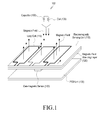
- a loop coil 110 is disposed on an electromagnetic sensing unit 115 and current is applied to the loop coil 110, such that a magnetic field is generated and the generated magnetic field is absorbed by the electromagnetic pen 102.
- the electromagnetic pen 102 includes a capacitor 100 and a coil 105 and emits the absorbed magnetic field at a predetermined frequency.
- the magnetic field generated by the loop coil 110 induces a current in the resonant circuit of the pen, and that induced current flowing in the pen's coil 105 generates a corresponding magnetic field.
- the magnetic field emitted by the electromagnetic pen 102 is absorbed by the loop coil 110 of the electromagnetic sensing unit 115, such that the electromagnetic sensing unit 115 determines which position of the pointing input device the electromagnetic pen 102 is close to.
- the electromagnetic sensing unit 115 includes a plurality of loop coils 110 which interact with the electromagnetic pen 102, and the plurality of loop coils 110 are disposed to overlap each other.
- the plurality of loop coils 110 senses a magnetic field generated from the electromagnetic pen 102.
- each of the plurality of loop coils 110 outputs a current induced by the sensed magnetic field.
- the loop coil 110 is disposed closer to the electromagnetic pen 102, it senses a magnetic field having a larger amplitude and emits a corresponding induced current.
- the plurality of loop coils 110 output induced currents of various magnitudes, such that by measuring the outputs of the loop coils 110, the position of the electromagnetic pen 102 is tracked.
- the pen's magnetic field (generated as a result of current induced in the pen by a magnetic field generated by a loop coil) affects (i.e. changes) the current in a loop coil over which the pen is positioned. This effect (change) can be detected, and is used as an indication of pen position.
- a magnetic field shielding layer 120 Under the electromagnetic sensing unit 115 is provided a magnetic field shielding layer 120. Under the magnetic field shielding layer 120 is provided a Printed Circuit Board (PCB) unit 130 in which a tool (which can be described as mounting means) for firmly mounting the pointing input device, a battery, and various circuit units, etc., are disposed.
- the magnetic field shielding layer 120 blocks a magnetic field generated from the circuit units, etc., disposed on the PCB unit 130 under the magnetic field shielding layer 120 to prevent magnetic field attenuation.
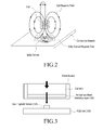
- FIG. 2 illustrates the principle of a magnetic field shielding layer.
- FIG. 2 assumes that a magnetic field is applied to metal, which is a conductive material having a low resistance, without a magnetic field shielding layer.
- metal which is a conductive material having a low resistance
- an eddy current is generated.
- the eddy current generates a magnetic field opposing the applied coil magnetic field, thus generating an eddy current magnetic field.
- the coil magnetic field is attenuated by the eddy current magnetic field and thus is reduced. Consequently, when a intensity of the magnetic field emitted by the electromagnetic pen 102 is reduced, a maximum distance required for sensing the magnetic field is reduced, increasing the probability of malfunction. That is, the electromagnetic pen 102 can be sensed within the maximum distance by the electromagnetic sensing unit 115.
- the magnetic field shielding layer 120 is used.
- the coil magnetic field does not reach under the magnetic field shielding layer 120, such that the eddy current is not generated even when a conductor exists under the magnetic field shielding layer 120, thereby preventing magnetic field attenuation. Consequently, the coil magnetic field reaches the electromagnetic sensing unit 115 near the magnetic field shielding layer 120, without magnetic field attenuation, such that the magnetic field induced by the electromagnetic pen 102 can be sensed.
- the magnetic field shielding layer for the pointing input device an alloy thin film composed of silicon (Si) based on iron (Fe) is used. Recently, amorphous metal made by mixing iron (Fe), Silicon (Si), and boron (B), while altering a crystal structure of the mixture, has been used.
- the amorphous metal is a material that has superior magnetic field shielding performance with high permeability and conductivity with respect to a magnetic field in a band of several hundreds of kHz and a low-frequency band that are generally used for a pointing input device.
- the amorphous metal has much higher permeability than other materials in DC (Direct Current).
- a geo-magnetic sensor 125 when a geo-magnetic sensor 125 is positioned near the magnetic field shielding layer 120 composed of the amorphous metal illustrated in FIG. 3 , Earth's magnetic field sensed by the geo-magnetic sensor 125 may be blocked or disturbed by the magnetic field shielding layer 120. In other words, due to the amorphous metal having high permeability in DC, the geo-magnetic sensor 125 has difficulty sensing Earth's magnetic field, which is a DC magnetic field.
- FIG. 4B An evaluation of characteristics of a geo-magnetic sensor when the amorphous metal is used is illustrated in FIG. 4B .
- graphs show outputs of the geo-magnetic sensor without and with an amorphous metal present, respectively, when a DC magnetic field is applied by rotating around the geo-magnetic sensor.
- the direction of the applied magnetic field is determined by a ratio of direction components of the geo-magnetic sensor output, that is, a ratio of outputs along X and Y axes of the graph. Therefore, to know an accurate magnetic field direction, the geo-magnetic sensor needs to have the same sensitivity for the magnetic field direction along the X and Y axes. For example, when the magnetic field is applied in a direction of 45 degrees, the strengths of the magnetic field measured on the respective axes have to be equal.
- the strengths of the magnetic field in the X and Y directions are such that one decreases if the other increases, and thus a vector sum of the two strengths forms a predetermined shape, i.e., a circle, as illustrated in FIG. 4A .
- FIG. 4B When a magnetic body exists near the geo-magnetic sensor, a center of the circle shown in FIG. 4A moves or the shape of the circle shown in FIG. 4A changes into an oval shape as illustrated in FIG. 4B .
- the graph shown in FIG. 4B indicates that the geo-magnetic sensor malfunctions due to blocking or disturbance of the Earth's magnetic field caused by the amorphous metal.
- the amorphous metal has a strong residual field, such that when a strong magnetic field is applied to the amorphous metal, the amorphous metal maintains a magnetized condition, thus serving as a permanent magnet. Subsequently, an influence upon the geo-magnetic sensor is continuously maintained.
- FIG. 5 illustrates permeability characteristics of amorphous metal with respect to frequency. Permeability shown in FIG. 5 is higher than 1,000 ⁇ 0 in a band of a frequency of 100 kHz or less. The ⁇ 0 is defined as the permeability in vacuum. It can be seen from FIG. 5 that an influence of amorphous metal upon the geo-magnetic sensor is significant.
- a pointing input device having a magnetic field sensing function such as in a geo-magnetic sensor, needs a magnetic field shielding layer that can perform a magnetic field shielding function without affecting the geo-magnetic sensor.
- An embodiment of the present invention provides a magnetic field shielding layer composed of a magnetic powder material.
- FIG. 6 illustrates characteristics of a magnetic powder material, the amorphous metal has a permeability of 170 ⁇ 0 or more in a 500 kHz band and has a permeability of 10,000 ⁇ 0 or more in a band of a frequency less than 500 kHz, as illustrated in FIG. 5 .
- Earth's magnetic field is blocked or disturbed by amorphous metal, such that the geo-magnetic sensor cannot operate to sense Earth's magnetic field.
- the magnetic powder material used in an embodiment of the present invention has a permeability of 100 ⁇ 0 in the 500kHz band and maintains this permeability over a large frequency area. Moreover, a similar permeability is provided in the DC band. Therefore, considering that the DC permeability of amorphous metal is higher than 10,000 ⁇ 0, the permeability of the magnetic powder material is 1/100 of that of the amorphous metal, such that the influence of the magnetic powder upon the geo-magnetic sensor is minimized.
- a magnetic field shielding layer may be formed to have a permeability of 150 ⁇ 0 by using the magnetic powder material.
- the magnetic field shielding layer has a permeability similar to that of the amorphous metal in a primary band without having a large influence upon the performance of the pointing input device, thereby blocking a magnetic field induced by an electromagnetic pen.
- the permeability of the magnetic powder material is maintained at a relatively low level across a large frequency area, such that Earth's magnetic field sensed by the geo-magnetic sensor is transmitted.
- FIG. 7 illustrates a form in which the magnetic field shielding layer composed of the magnetic powder material is disposed according to an embodiment of the present invention.
- FIG. 7 is a cross-sectional view of the pointing input device shown in FIG. 1 .
- the pointing input device includes a display unit 700, the electromagnetic sensing unit 115, the magnetic field shielding layer 120, the geo-magnetic sensor 125, and the PCB unit 130.
- the display unit 700 is a region for displaying visual information recognizable by a user.
- the display unit 700 receives an external input of a control signal or a graphic signal and displays a display screen corresponding to the control signal or the graphic signal.
- the display unit 700 is preferably a Liquid Crystal Display (LCD) module, but there is no limit on a type of the display unit 700, as can be easily understood by those of ordinary skill in the art.
- LCD Liquid Crystal Display
- the electromagnetic sensing unit 115 is disposed adjacent to a bottom surface of the display unit 700.
- a structure of the electromagnetic sensing unit 115 is the same as described above with reference to FIG. 1 .
- the electromagnetic sensing unit 115 senses electromagnetism incident from an electromagnetic pen, which approaches or contacts a top surface of the display unit 700, thereby determining a point selected by the user.
- the geo-magnetic sensor 125 is disposed in the pointing input device, and senses a part of Earth's magnetic field applied through the magnetic field shielding layer 120.
- the geo-magnetic sensor 125 is positioned under the magnetic field shielding layer 120 which is not affected by the magnetic field of the electromagnetic pen.
- the geo-magnetic sensor 125 is disposed on the PCB unit 130.
- the PCB unit 130 includes various electronic components capable of electrically operating and controlling the pointing input device.
- the magnetic field including electromagnetic waves generated from the various electronic parts of the PCB unit 130 is blocked by the magnetic field shielding layer 120 composed of the magnetic powder material.
- the magnetic field shielding layer 120 is composed of a magnetic powder material, and is disposed under the electromagnetic sensing unit 115.
- the magnetic field shielding layer 120 is a partial shielding layer capable of partially transmitting the applied magnetic field, and is formed by distributing (e.g. scattering) the magnetic powder.
- Magnetic metal powder called ferrite, MolyPermalloy Powder (MPP), a Fe-Si-Al-based material (Sandust), a Ni-Fe-based material (Highflux), or the like may be used.
- the magnetic powder is in the form of a powder, it is spread after being mixed with an adhesive such as a polymer (ex: PP(Polypropylene), PE(Polyethylene), etc.)
- an adhesive such as a polymer (ex: PP(Polypropylene), PE(Polyethylene), etc.)
- Amorphous metal powder and the magnetic powder are preferably used together, and the magnetic metal powder and the amorphous metal powder are mixed with an adhesive to form the magnetic field shielding layer 120.
- the magnetic field shielding layer 120 formed of the magnetic powder has a different permeability and a different density of the magnetic powder. As the density of the magnetic powder increases, the permeability of the magnetic field shielding layer 120 increases. Thus, the density of the magnetic powder of the magnetic field shielding layer 120 is adjusted to obtain a permeability similar to that when a metal thin film is used, but unlike when the metal thin film is used, Earth's magnetic field is transmitted, such that the operation of the geo-magnetic sensor 125 is not affected.
- the permeability of the magnetic field shielding layer 120 differs according to a mixing ratio of magnetic powder mixed with polymer to form the magnetic field shielding layer 120, i.e., a density of the magnetic powder.
- the density of the magnetic powder i.e., the mixing ratio is preferably set such that the permeability of the magnetic field shielding layer 120 is 100 - 200 ⁇ 0 in the DC band.
- Such a magnetic powder is mixed with an adhesive, and adhered to the electromagnetic sensing unit 115.
- the magnetic field shielding layer 120 does not need a separate adhesive layer, contributing to a reduction in thickness.
- the magnetic powder material is in a liquid state when mixed with the adhesive, and can thus be uniformly spread on the electromagnetic sensing unit 115.
- the magnetic powder material is uniformly spread, such that uniform shielding performance can be obtained over the entire surface of the magnetic field shielding layer 120.
- the magnetic field shielding layer 120 is directly adhered to the pointing input device without a separate adhesive layer, simplifying processing and reducing an extra thickness corresponding to the thickness of the conventional adhesive layer.
- the magnetic powder material may be coated to, e.g., a surface of the electromagnetic sensing unit 115 in the pointing input device.
- the magnetic powder material may be coated onto an adhesive film having adhesion and then onto a surface in the pointing input device.
- a residual magnetic field of the magnetic powder material is not strong, unlike when using the amorphous metal thin film, such that even when a strong magnetic field is applied to the magnetic powder material, the magnetic powder material does not affect the operation of the geo-magnetic sensor.
- the pointing input device having the magnetic field shielding layer 120 using the magnetic powder material when placed on a magnetic field disturbing material such as a conductor, may experience degradation in sensitivity due to an influence of an eddy current, generation of a magnetic field, or degradation of absorbing characteristics.
- sensitivity degradation is relative to the amorphous metal thin film, and has a proper level of sensitivity for the pointing input device illustrated in FIG. 11 .
- FIG. 11 is a graph illustrating sensitivity comparison when amorphous metal and magnetic powder are used according to an embodiment of the present invention.
- a signal strength of a touch screen which uses a magnetic powder material having a permeability of 150 ⁇ 0 and a thickness of 50 ⁇ m and a amorphous metal thin film having a thickness of 25 ⁇ m is measured.
- the magnetic powder material may have a lower sensitivity than the amorphous metal thin film, but its sensitivity may be adjusted by adjusting a thickness to obtain a desired sensitivity.
- the thickness of the magnetic field shielding layer 120 is preferably 50 ⁇ m or more. Since the permeability of the magnetic field shielding layer 120 varies according to the thickness of the magnetic field shielding layer 120, the thickness is be set as according to the desired permeability.
- a magnetic field shielding layer is formed as illustrated in FIG. 8 .
- a magnetic field shielding layer 805 using magnetic powder i.e., a magnetic powder shielding layer
- a magnetic field shielding layer 810 using an amorphous metal thin film i.e., an amorphous metal shielding layer
- the magnetic powder shielding layer 805 is disposed around the geo-magnetic sensor 800 to guarantee the normal operation of the geo-magnetic sensor 800 and the amorphous metal shielding layer 810 is disposed on the other area to improve sensitivity.
- FIG. 9 illustrates a cross-section of the arrangement of the magnetic powder shielding layer 805 and the amorphous metal shielding layer 810, including a display unit 815.
- the magnetic field shielding layer includes the magnetic powder shielding layer 805 in which magnetic powder for partially transmitting the applied Earth's magnetic field is scattered, and the amorphous metal shielding layer 810, which uses the amorphous metal thin film for blocking the applied magnetic field.
- the positions of the magnetic powder shielding layer 805 and the amorphous metal shielding layer 810 change according to the position of the geo-magnetic sensor 800.
- a portion of the entire magnetic field shielding layer corresponding to the position of the geo-magnetic sensor 800 is formed as the magnetic powder shielding layer 805 using the magnetic powder.
- the low-frequency magnetic field such as Earth's magnetic field
- sensed by the geo-magnetic sensor 800 is transmitted, but transmission of a magnetic field of a frequency used for pointing is restricted.
- the other portion of the magnetic field shielding layer is formed of the amorphous metal shielding layer 810 preventing a magnetic field generated according to arrangement of a tool, a battery, various circuit units, and so forth, on which the pointing input device is mounted.
- the amorphous metal shielding layer 810 is formed in a region other than a region where the magnetic powder shielding layer 805 is formed, as shown in FIGs. 8 and 9 , such that Earth's magnetic field is partially blocked by the amorphous metal shielding layer 810, degrading the performance of the geo-magnetic sensor 800 when compared to the structure of the magnetic field shielding layer 120 shown in FIG. 7 .
- the entire magnetic field shielding layer 120 is formed of the magnetic powder, regardless of the position of the geo-magnetic sensor 125, such that the magnetic powder shielding layer 120 does not block the Earth's magnetic field and therefore does not affect the performance of the geo-magnetic sensor 125.
- an embodiment of the present invention provides a structure of a magnetic field shielding layer illustrated in FIG. 12 .
- the embodiment of the present invention illustrated in FIG. 12 provides a structure of a magnetic field shielding layer where a magnetic part for generating a strong low-frequency magnetic field, other than a geo-magnetic sensor, is mounted.
- a speaker and a camera 1230 are mounted as examples of the magnetic parts 1230 on a side of the PCB unit 130 in FIG. 12
- the magnetic parts 1230 are also disposed on the PCB unit 130.
- a magnetic field generated in the magnetic parts 1230 passes through the magnetic powder shielding layer, thus affecting the performance of the pointing input device.
- a magnetic field generated in a magnetic part changes frequency and strength of a signal generated in a pen, interrupting the operation of the pen.
- a magnetic field shielding layer having a superior shielding property such as amorphous metal
- replaces the magnetic powder shielding layer 120 shown in FIG. 7 to block the magnetic field generated in the magnetic part the amorphous metal shielding layer affects the performance of the geo-magnetic sensor 125.
- the embodiment of the present invention illustrated in FIG. 12 provides a structure, which effectively blocks the magnetic field generated by the magnetic parts 1230 without affecting the performance of the geo-magnetic sensor 800.
- a structure of the magnetic field shielding layer illustrated in FIG. 12 is different from the structure of the magnetic field shielding layer shown in FIG. 7 in that an amorphous metal shielding layer 1220 is disposed under a magnetic powder shielding layer 1210 and in proximity to a magnetic part which generates a strong low-frequency magnetic field, e.g., a speaker/camera 1230.
- the amorphous metal shielding layer 1220 is disposed under the magnetic powder shielding layer 1210 formed on a surface of the electromagnetic sensing unit 115 and in proximity to the speaker/camera 1230 by closely contacting the magnetic powder shielding layer 1210.
- the amorphous metal shielding layer 1220 closely contacts a portion of the surface of the magnetic powder shielding layer 1210 rather than the entire surface thereof, and the size and position of the amorphous metal shielding layer 1220 is such that it can block the magnetic field generated by the magnetic parts 1230, and thus varies according to the size and position of the magnetic part.
- the magnetic field shielding layer prevents a magnetic field generated by the electromagnetic pen from reaching a conductor positioned under the magnetic field shielding layer, and minimizes influence upon an operation of the geo-magnetic sensor installed in the pointing input device.
- the electromagnetic shielding layer is formed directly in the pointing input device without a separate adhesive layer, thereby reducing the thickness of the pointing input device.
- embodiments of the present invention minimize influence upon the geo-magnetic sensor and maximize sensitivity of the geo-magnetic sensor by using a mixture of different magnetic powders.
- the magnetic field shielding layer having a low magnetic field shielding property such as a magnetic powder material and the magnetic field shielding layer having a superior shielding property such as amorphous metal are arranged according to the positions of the geo-magnetic sensor, the speaker, and the camera, guaranteeing both the performance of the geo-magnetic sensor and the performance of the pointing input device.
Landscapes
- Engineering & Computer Science (AREA)
- General Engineering & Computer Science (AREA)
- Theoretical Computer Science (AREA)
- Physics & Mathematics (AREA)
- General Physics & Mathematics (AREA)
- Human Computer Interaction (AREA)
- Remote Sensing (AREA)
- Power Engineering (AREA)
- Life Sciences & Earth Sciences (AREA)
- Electromagnetism (AREA)
- Environmental & Geological Engineering (AREA)
- Geology (AREA)
- General Life Sciences & Earth Sciences (AREA)
- Geophysics (AREA)
- Shielding Devices Or Components To Electric Or Magnetic Fields (AREA)
- Position Input By Displaying (AREA)
Applications Claiming Priority (2)
| Application Number | Priority Date | Filing Date | Title |
|---|---|---|---|
| KR20110068641 | 2011-07-11 | ||
| KR1020110105362A KR101804579B1 (ko) | 2011-07-11 | 2011-10-14 | 입력 장치 |
Publications (2)
| Publication Number | Publication Date |
|---|---|
| EP2546732A2 true EP2546732A2 (de) | 2013-01-16 |
| EP2546732A3 EP2546732A3 (de) | 2015-12-09 |
Family
ID=47002511
Family Applications (1)
| Application Number | Title | Priority Date | Filing Date |
|---|---|---|---|
| EP12175979.9A Ceased EP2546732A3 (de) | 2011-07-11 | 2012-07-11 | Eingabegerät |
Country Status (4)
| Country | Link |
|---|---|
| US (2) | US9001088B2 (de) |
| EP (1) | EP2546732A3 (de) |
| CN (1) | CN102879830B (de) |
| WO (1) | WO2013009071A2 (de) |
Cited By (1)
| Publication number | Priority date | Publication date | Assignee | Title |
|---|---|---|---|---|
| EP2830074A3 (de) * | 2013-07-26 | 2015-02-25 | Wacom Co., Ltd. | Elektromagnetischer Induktionssensor, Überzugselement für einen elektromagnetischen Induktionssensor, und Herstellungsverfahren für einen elektromagnetischen Induktionssensor |
Families Citing this family (18)
| Publication number | Priority date | Publication date | Assignee | Title |
|---|---|---|---|---|
| KR101703842B1 (ko) * | 2013-03-05 | 2017-02-08 | 주식회사 아모센스 | 자기장 및 전자파 차폐용 복합시트 및 이를 구비하는 안테나 모듈 |
| KR102027246B1 (ko) * | 2013-03-14 | 2019-10-01 | 삼성전자주식회사 | 디지타이저 및 그 제조 방법 |
| US9952703B2 (en) | 2013-03-15 | 2018-04-24 | Apple Inc. | Force sensing of inputs through strain analysis |
| US20140320369A1 (en) * | 2013-04-24 | 2014-10-30 | Broadcom Corporation | Shielding layer for a device having a plurality of antennas |
| TWI489327B (zh) * | 2013-07-25 | 2015-06-21 | Waltop Int Corp | 電磁感應壓力階度的修正方法 |
| KR102213899B1 (ko) * | 2013-12-03 | 2021-02-08 | 삼성전자주식회사 | 전자 디바이스 및 전자 디바이스의 커버와 전자 디바이스에서 기능 실행 방법 |
| AU2015100011B4 (en) | 2014-01-13 | 2015-07-16 | Apple Inc. | Temperature compensating transparent force sensor |
| KR102178558B1 (ko) * | 2014-01-22 | 2020-11-16 | 삼성디스플레이 주식회사 | 접촉 감지 장치 및 접촉 감지 방법 |
| CN106515126B (zh) * | 2016-11-08 | 2018-11-02 | 广东小天才科技有限公司 | 磁性叠层结构、磁性叠层结构的制备方法及输入装置 |
| CN107066165B (zh) * | 2017-02-13 | 2018-06-12 | 深圳市华鼎星科技有限公司 | 一种阵列编码磁信号定位感应装置 |
| US10444091B2 (en) | 2017-04-11 | 2019-10-15 | Apple Inc. | Row column architecture for strain sensing |
| US10309846B2 (en) * | 2017-07-24 | 2019-06-04 | Apple Inc. | Magnetic field cancellation for strain sensors |
| JP6487089B2 (ja) * | 2018-03-16 | 2019-03-20 | 株式会社ワコム | 電磁誘導方式のセンサの製法 |
| US10782818B2 (en) | 2018-08-29 | 2020-09-22 | Apple Inc. | Load cell array for detection of force input to an electronic device enclosure |
| KR20230006141A (ko) | 2021-07-02 | 2023-01-10 | 삼성전자주식회사 | 차폐 부재 및 차폐 부재를 포함하는 전자 장치 |
| EP4332737A4 (de) | 2021-07-27 | 2024-10-30 | Samsung Electronics Co., Ltd. | Digitalisierer und elektronische vorrichtung damit |
| KR20230158864A (ko) * | 2022-05-12 | 2023-11-21 | 주식회사 하이딥 | 스타일러스 펜 |
| US12307062B2 (en) * | 2023-05-30 | 2025-05-20 | Cirque Corporation | Coil shield of a capacitance module |
Family Cites Families (30)
| Publication number | Priority date | Publication date | Assignee | Title |
|---|---|---|---|---|
| US3458802A (en) * | 1966-05-02 | 1969-07-29 | Bunker Ramo | Magnetic vehicle detection system including feedback means for eliminating spurious presence indications |
| JP2566295B2 (ja) | 1988-08-12 | 1996-12-25 | 松下電工株式会社 | Gps受信用アンテナ |
| JPH1049287A (ja) * | 1996-07-29 | 1998-02-20 | Wacom Co Ltd | 位置検出装置のタブレット |
| JP2001337614A (ja) * | 2000-05-29 | 2001-12-07 | Nitto Denko Corp | プラズマデイスプレイパネル用フイルタ、プラズマデイスプレイパネル用前面板およびプラズマデイスプレイパネル表示装置 |
| US6673199B1 (en) * | 2001-03-07 | 2004-01-06 | Applied Materials, Inc. | Shaping a plasma with a magnetic field to control etch rate uniformity |
| JP3721141B2 (ja) * | 2002-03-25 | 2005-11-30 | 松下電器産業株式会社 | 携帯端末装置 |
| US7142197B2 (en) | 2002-10-31 | 2006-11-28 | Microsoft Corporation | Universal computing device |
| JP2004272365A (ja) * | 2003-03-05 | 2004-09-30 | Seiko Epson Corp | 電気光学パネル、電気光学装置、電気光学パネルの製造方法、電気光学装置の製造方法および電磁誘導センサ、並びに電子機器 |
| CN2731554Y (zh) * | 2004-07-12 | 2005-10-05 | 金昊 | 智能电磁式电子白板 |
| KR100963045B1 (ko) * | 2006-04-27 | 2010-06-14 | 삼성코닝정밀소재 주식회사 | 디스플레이 장치용 광학 필터 및 이를 포함하는 디스플레이장치 |
| JP2008211169A (ja) * | 2007-02-02 | 2008-09-11 | Tdk Corp | シート状磁性体およびシート状磁性体の製造方法 |
| US7511487B2 (en) * | 2007-02-27 | 2009-03-31 | Schlumberger Technology Corporation | Logging method for determining characteristic of fluid in a downhole measurement region |
| JP4972782B2 (ja) * | 2007-06-22 | 2012-07-11 | 株式会社ワコム | 位置検出装置 |
| US8922160B2 (en) * | 2007-08-21 | 2014-12-30 | Kabushiki Kaisha Toshiba | Non-contact type power receiving apparatus, electronic equipment and charging system using the power receiving apparatus |
| CN101408816B (zh) * | 2007-10-12 | 2010-12-29 | 群康科技(深圳)有限公司 | 触摸屏、触摸屏的驱动方法和触摸屏显示装置 |
| CN101226801A (zh) * | 2007-11-27 | 2008-07-23 | 浙江大学 | 铁基合金抗电磁干扰材料的制备方法 |
| JP5104426B2 (ja) * | 2008-03-13 | 2012-12-19 | パナソニック株式会社 | 画像表示装置 |
| RU75077U1 (ru) | 2008-03-28 | 2008-07-20 | Общество с ограниченной ответственностью "Технические системы - сервис, качество и надежность" | Промышленный защищенный карманный компьютер |
| US8042949B2 (en) * | 2008-05-02 | 2011-10-25 | Microsoft Corporation | Projection of images onto tangible user interfaces |
| KR101244022B1 (ko) * | 2008-09-04 | 2013-03-14 | 쓰리엠 이노베이티브 프로퍼티즈 캄파니 | 전자기파간섭 억제용 복합시트 |
| US8253713B2 (en) * | 2008-10-23 | 2012-08-28 | At&T Intellectual Property I, L.P. | Tracking approaching or hovering objects for user-interfaces |
| JP5159696B2 (ja) | 2009-05-12 | 2013-03-06 | 日本写真印刷株式会社 | 位置検知入力装置および位置検知算出方法 |
| JP5556101B2 (ja) | 2009-09-17 | 2014-07-23 | ソニー株式会社 | 方位算出装置、補正値初期化方法及び方位算出機能付携帯電話機 |
| CN102053770A (zh) * | 2009-11-03 | 2011-05-11 | 太瀚科技股份有限公司 | 电磁手写功能显示器 |
| JP5427070B2 (ja) * | 2010-03-05 | 2014-02-26 | 株式会社ワコム | 位置検出装置 |
| TWI424386B (zh) * | 2010-03-19 | 2014-01-21 | Prime View Int Co Ltd | 雙態顯示器 |
| KR101148531B1 (ko) * | 2010-04-26 | 2012-05-21 | 삼성전기주식회사 | 터치스크린 |
| US8390411B2 (en) * | 2010-09-17 | 2013-03-05 | Apple Inc. | Tablet device |
| US8344836B2 (en) * | 2010-09-17 | 2013-01-01 | Apple Inc. | Protective cover for a tablet computer |
| JP5459795B2 (ja) * | 2011-06-06 | 2014-04-02 | 株式会社ワコム | 電子機器 |
-
2012
- 2012-07-10 WO PCT/KR2012/005460 patent/WO2013009071A2/en not_active Ceased
- 2012-07-11 CN CN201210240680.5A patent/CN102879830B/zh not_active Expired - Fee Related
- 2012-07-11 EP EP12175979.9A patent/EP2546732A3/de not_active Ceased
- 2012-07-11 US US13/546,608 patent/US9001088B2/en active Active
-
2015
- 2015-04-02 US US14/677,598 patent/US9626038B2/en not_active Expired - Fee Related
Non-Patent Citations (1)
| Title |
|---|
| None |
Cited By (3)
| Publication number | Priority date | Publication date | Assignee | Title |
|---|---|---|---|---|
| EP2830074A3 (de) * | 2013-07-26 | 2015-02-25 | Wacom Co., Ltd. | Elektromagnetischer Induktionssensor, Überzugselement für einen elektromagnetischen Induktionssensor, und Herstellungsverfahren für einen elektromagnetischen Induktionssensor |
| US9441992B2 (en) | 2013-07-26 | 2016-09-13 | Wacom Co., Ltd. | Electromagnetic induction sensor, overlay member for electromagnetic induction sensor, and manufacturing method of electromagnetic induction sensor |
| US10054466B2 (en) | 2013-07-26 | 2018-08-21 | Wacom Co., Ltd. | Electromagnetic induction sensor, overlay member for electromagnetic induction sensor, and manufacturing method of electromagnetic induction sensor |
Also Published As
| Publication number | Publication date |
|---|---|
| US9001088B2 (en) | 2015-04-07 |
| US20130016073A1 (en) | 2013-01-17 |
| WO2013009071A3 (en) | 2013-03-14 |
| US20150212651A1 (en) | 2015-07-30 |
| WO2013009071A2 (en) | 2013-01-17 |
| US9626038B2 (en) | 2017-04-18 |
| EP2546732A3 (de) | 2015-12-09 |
| CN102879830A (zh) | 2013-01-16 |
| CN102879830B (zh) | 2018-04-27 |
Similar Documents
| Publication | Publication Date | Title |
|---|---|---|
| US9001088B2 (en) | Input device | |
| AU2012281363B2 (en) | Input device | |
| US10168848B2 (en) | Radiofrequency-wave-transparent capacitive sensor pad | |
| KR101975596B1 (ko) | 입력 감지 신호 왜곡 보상 구조를 가지는 터치스크린 장치 | |
| EP2015030B1 (de) | Positionsdetektor und Anzeigevorrichtung | |
| EP2533139B1 (de) | Positionserkennungsvorrichtung, Anzeigevorrichtung und tragbare Vorrichtung | |
| US8487905B2 (en) | Electrode arrangement for display device | |
| US20190384449A1 (en) | Method and apparatus for limiting a sensing region of a capacitive sensing electrode | |
| US9939956B2 (en) | Capacitive sensing device comprising perforated electrodes | |
| JP5153890B2 (ja) | タッチパネルおよびタッチパネルを備えた電子機器 | |
| US20250364172A1 (en) | Grounded Ferrite in Wireless Power Systems | |
| US12535888B2 (en) | Capacitance module with an antenna and haptics | |
| CN113376701A (zh) | 天线模组、温度变化的检测方法及装置和相关应用 | |
| JP7233856B2 (ja) | 位置検出センサ | |
| CN113994307B (zh) | 位置检测装置 | |
| KR102158709B1 (ko) | 접촉 감지 장치 및 이의 컨트롤러 ic | |
| US12248648B2 (en) | Magnetically conductive electrically insulating material in a capacitance module | |
| KR20150017224A (ko) | 입력 장치 및 그를 포함하는 전자 장치 | |
| US10814589B1 (en) | Items having leatherboard layers with modified portions | |
| KR20130131092A (ko) | 좌표 표시 장치의 입력 좌표를 측정하는 좌표 측정 장치 | |
| Ko et al. | Alignment Free Power Transfer System for IoT Devices |
Legal Events
| Date | Code | Title | Description |
|---|---|---|---|
| PUAI | Public reference made under article 153(3) epc to a published international application that has entered the european phase |
Free format text: ORIGINAL CODE: 0009012 |
|
| AK | Designated contracting states |
Kind code of ref document: A2 Designated state(s): AL AT BE BG CH CY CZ DE DK EE ES FI FR GB GR HR HU IE IS IT LI LT LU LV MC MK MT NL NO PL PT RO RS SE SI SK SM TR |
|
| AX | Request for extension of the european patent |
Extension state: BA ME |
|
| PUAL | Search report despatched |
Free format text: ORIGINAL CODE: 0009013 |
|
| AK | Designated contracting states |
Kind code of ref document: A3 Designated state(s): AL AT BE BG CH CY CZ DE DK EE ES FI FR GB GR HR HU IE IS IT LI LT LU LV MC MK MT NL NO PL PT RO RS SE SI SK SM TR |
|
| AX | Request for extension of the european patent |
Extension state: BA ME |
|
| RIC1 | Information provided on ipc code assigned before grant |
Ipc: G06F 3/033 20130101ALI20151104BHEP Ipc: G06F 3/046 20060101AFI20151104BHEP Ipc: G06F 3/0354 20130101ALI20151104BHEP |
|
| 17P | Request for examination filed |
Effective date: 20160609 |
|
| STAA | Information on the status of an ep patent application or granted ep patent |
Free format text: STATUS: REQUEST FOR EXAMINATION WAS MADE |
|
| R17P | Request for examination filed (corrected) |
Effective date: 20160609 |
|
| STAA | Information on the status of an ep patent application or granted ep patent |
Free format text: STATUS: EXAMINATION IS IN PROGRESS |
|
| 17Q | First examination report despatched |
Effective date: 20170822 |
|
| STAA | Information on the status of an ep patent application or granted ep patent |
Free format text: STATUS: THE APPLICATION HAS BEEN REFUSED |
|
| 18R | Application refused |
Effective date: 20190304 |