EP2546621A1 - Vorrichtung und Verfahren zum Detektieren von Licht - Google Patents
Vorrichtung und Verfahren zum Detektieren von Licht Download PDFInfo
- Publication number
- EP2546621A1 EP2546621A1 EP12174314A EP12174314A EP2546621A1 EP 2546621 A1 EP2546621 A1 EP 2546621A1 EP 12174314 A EP12174314 A EP 12174314A EP 12174314 A EP12174314 A EP 12174314A EP 2546621 A1 EP2546621 A1 EP 2546621A1
- Authority
- EP
- European Patent Office
- Prior art keywords
- spads
- light
- sipm
- array
- spad
- Prior art date
- Legal status (The legal status is an assumption and is not a legal conclusion. Google has not performed a legal analysis and makes no representation as to the accuracy of the status listed.)
- Granted
Links
Images





Classifications
-
- G—PHYSICS
- G01—MEASURING; TESTING
- G01J—MEASUREMENT OF INTENSITY, VELOCITY, SPECTRAL CONTENT, POLARISATION, PHASE OR PULSE CHARACTERISTICS OF INFRARED, VISIBLE OR ULTRAVIOLET LIGHT; COLORIMETRY; RADIATION PYROMETRY
- G01J3/00—Spectrometry; Spectrophotometry; Monochromators; Measuring colours
- G01J3/02—Details
- G01J3/027—Control of working procedures of a spectrometer; Failure detection; Bandwidth calculation
-
- G—PHYSICS
- G01—MEASURING; TESTING
- G01J—MEASUREMENT OF INTENSITY, VELOCITY, SPECTRAL CONTENT, POLARISATION, PHASE OR PULSE CHARACTERISTICS OF INFRARED, VISIBLE OR ULTRAVIOLET LIGHT; COLORIMETRY; RADIATION PYROMETRY
- G01J1/00—Photometry, e.g. photographic exposure meter
- G01J1/02—Details
- G01J1/0228—Control of working procedures; Failure detection; Spectral bandwidth calculation
-
- G—PHYSICS
- G01—MEASURING; TESTING
- G01J—MEASUREMENT OF INTENSITY, VELOCITY, SPECTRAL CONTENT, POLARISATION, PHASE OR PULSE CHARACTERISTICS OF INFRARED, VISIBLE OR ULTRAVIOLET LIGHT; COLORIMETRY; RADIATION PYROMETRY
- G01J1/00—Photometry, e.g. photographic exposure meter
- G01J1/10—Photometry, e.g. photographic exposure meter by comparison with reference light or electric value provisionally void
- G01J1/16—Photometry, e.g. photographic exposure meter by comparison with reference light or electric value provisionally void using electric radiation detectors
- G01J1/18—Photometry, e.g. photographic exposure meter by comparison with reference light or electric value provisionally void using electric radiation detectors using comparison with a reference electric value
-
- G—PHYSICS
- G01—MEASURING; TESTING
- G01J—MEASUREMENT OF INTENSITY, VELOCITY, SPECTRAL CONTENT, POLARISATION, PHASE OR PULSE CHARACTERISTICS OF INFRARED, VISIBLE OR ULTRAVIOLET LIGHT; COLORIMETRY; RADIATION PYROMETRY
- G01J1/00—Photometry, e.g. photographic exposure meter
- G01J1/42—Photometry, e.g. photographic exposure meter using electric radiation detectors
- G01J1/44—Electric circuits
-
- G—PHYSICS
- G01—MEASURING; TESTING
- G01J—MEASUREMENT OF INTENSITY, VELOCITY, SPECTRAL CONTENT, POLARISATION, PHASE OR PULSE CHARACTERISTICS OF INFRARED, VISIBLE OR ULTRAVIOLET LIGHT; COLORIMETRY; RADIATION PYROMETRY
- G01J3/00—Spectrometry; Spectrophotometry; Monochromators; Measuring colours
- G01J3/28—Investigating the spectrum
- G01J3/2803—Investigating the spectrum using photoelectric array detector
-
- G—PHYSICS
- G01—MEASURING; TESTING
- G01J—MEASUREMENT OF INTENSITY, VELOCITY, SPECTRAL CONTENT, POLARISATION, PHASE OR PULSE CHARACTERISTICS OF INFRARED, VISIBLE OR ULTRAVIOLET LIGHT; COLORIMETRY; RADIATION PYROMETRY
- G01J3/00—Spectrometry; Spectrophotometry; Monochromators; Measuring colours
- G01J3/28—Investigating the spectrum
- G01J3/30—Measuring the intensity of spectral lines directly on the spectrum itself
- G01J3/36—Investigating two or more bands of a spectrum by separate detectors
-
- G—PHYSICS
- G02—OPTICS
- G02B—OPTICAL ELEMENTS, SYSTEMS OR APPARATUS
- G02B21/00—Microscopes
- G02B21/0004—Microscopes specially adapted for specific applications
- G02B21/002—Scanning microscopes
- G02B21/0024—Confocal scanning microscopes (CSOMs) or confocal "macroscopes"; Accessories which are not restricted to use with CSOMs, e.g. sample holders
- G02B21/008—Details of detection or image processing, including general computer control
Definitions
- the invention relates to a device for detecting light, in particular for use in a microscope, in a spectrometer or in a camera. Furthermore, the invention relates to a corresponding method, preferably using the device.
- the invention is generally concerned with the detection of light, for example for use in a microscope, in a spectrometer or in a camera.
- the claimed device is not application specific. It is to be understood in the broadest sense as a detector for light.
- photomultipliers have been known in practice, which are special electron tubes, with the task of detecting weak light signals down to individual photons by generating and amplifying an electrical signal.
- a photomultiplier consists of a photocathode and a downstream photomultiplier placed in an evacuated glass envelope. Since the photomultiplier is a tube device, it builds relatively large, so it is not suitable for miniaturization.
- avalanche photodiodes or avalanche photodiodes (APDs) are known in practice, these being highly sensitive and fast photodiodes. They use the internal photoelectric effect to generate charge carriers and avalanche breakdown (avalanche effect) for internal amplification. APDs are considered the semiconductor equivalent to photomultipliers and find among others. Application in the detection of very low radiation power with cut-off frequencies up to the gigahertz range.
- APDs are operated in Geiger mode, whereby one speaks regularly of single photon avalanche diodes (SPAD).
- SiPM silicone photomultipliers
- PDE photon detection probability
- Photomultiplier tubes are more complex in construction than detectors made with Si technology.
- photomultipliers typically have a lower photon detection probability than avalanche photodiodes, for example.
- the dark noise is significantly dependent on the total detection area, the quality of the photocathode material and the operating temperature of the detector.
- the present invention is based on the object of specifying a device for detecting light and a corresponding method, according to which a high image quality or the highest possible signal-to-noise ratio can be achieved for a given illumination / light intensity.
- the device should be as small as possible and inexpensive to manufacture.
- the device for detecting light in particular in a microscope, in a spectrometer or in a camera, is equipped with at least one silicon photomultiplier (SiPM).
- the silicon photomultiplier consists of an arrangement or an array of several single photon avalanche diodes (SPAD).
- SPAD single photon avalanche diodes
- Essential to the invention is that the array has a larger area than the incident light, and only those SPADs are activated and / or evaluated that are actually acted upon or taken with a certain - high-minimum intensity of light.
- the device comprises a specially adapted SiPM, wherein the structure of the SiPM has a high photon detection probability (PDE), namely as in single photon avalanche diodes (SPAD).
- PDE photon detection probability
- SPAD single photon avalanche diodes
- the dynamics of a single pixel is determined by the number of SPADs combined per pixel and the dead time of a single SPAD.
- the dead time can be kept very short by means of "active quenching", namely in the range> 100 SPAD per pixel and ⁇ 50 ns dead time.
- the SiPMs used here offer the option of selectively activating or deactivating individual SPADs of a pixel.
- a SiPM with digital evaluation electronics is suitable for this purpose.
- an addressable static memory can be used to selectively activate individual SPADs directly on a chip.
- SiPMs can be produced in a conventional CMOS process. Accordingly, such silicon photomultipliers are extremely robust, especially with respect to high or too high light outputs.
- the device according to the invention comprises a plurality of silicon photomultipliers, each consisting of an array of several single photon avalanche diodes.
- the plurality of SiPMs may be arranged in a matrix, for example for use in a camera, or linearly adjacent to one another, for example for use in a spectrometer.
- the arrangement of the SiPMs overall has a larger area than the incident light, wherein only those SPADs of the different SiPMs within the arrangement are activated and / or evaluated, which impinges or illuminates with a certain - high - minimum intensity of light become.
- the device may comprise a single silicon photomultiplier with an array of SPADs or an array of multiple SiPMs, each with an array of SPADs.
- the minimum intensity of light can be determined from one or more sample measurements or a calibration at the respective preset system setting.
- the dark noise is caused to a very particular degree by defects in the photosensitive layer of the SPADs.
- a defective SPAD provides an electronic signal, although no light has hit the photosensitive area of the diode.
- the probability of such misconduct is called the dark count rate, which should be kept as low as possible.
- the teaching of the invention also relates to a device for detecting light, in particular for use in a microscope, in a spectrometer or in a camera, with at least one silicon photomultiplier (SiPM), the arrangement of an array of single photon avalanche diodes (SPAD), whereby for each SiPM those SPADs are deactivated or not evaluated whose function is insufficient or erroneous, which thus does not perform properly.
- SiPM silicon photomultiplier
- SPAD single photon avalanche diodes
- the inadequate or erroneous function of individual SPADs can be predefined by a lower threshold value of the ratio of useful signal to dark noise, whereby here it does not depend on a fixed threshold value.
- the insufficiently illuminated or insufficiently or incorrectly functioning SPADs can be determined by means of sample / calibration measurements so that deactivation of the defective SPADs is possible over the entire service life of the SiPM. It is further possible to create a type of illumination intensity map or dark noise map of the chip, for example sequentially activating only a portion of the SPADs per pixel and preferably only one SPAD per pixel at a time, so that the dark count rate is based on the pixel count rate individual SPADs can be assigned. In order to keep the areal proportion of the pixels to be deactivated as small as possible, it may be advantageous to use as many small SPADs as possible instead of less large SPADs per pixel.
- the SPADs to be deactivated are deactivated via a controller, preferably by programming technology, so that no mechanical intervention in the arrangement is required.
- the photosensitive content of the total illuminated area is significantly less than 100%, typically in the range between 50% and 70%. This results in a lower photon detection probability, namely due to the light-insensitive areas.
- the SPADs of a SiPM microlens or a microlens array tuned to the arrangement of the SPADs can be assigned in a particularly advantageous manner.
- the microlenses focus the incident on the entire array light on the respective photosensitive areas of the SPADs, so that can be increased by this measure, the fill factor.
- the geometry of the incident light given a SiPM geometry, it may also be useful to disable individual SPADs that would no longer be hit by the focused light, regardless of microlens precautions.
- the SPADs can be arranged on a chip, preferably made of a silicon substrate.
- a chip preferably made of a silicon substrate.
- An application of the device according to the invention in confocal microscopes is of particular advantage, wherein there, for example, fluorescence light coming from a sample is spectrally selective to detect.
- fluorescence light coming from a sample is spectrally selective to detect.
- the device according to the invention can also be used in a spectrometer, it being known in the context of such an application which diode belongs to the respective desired spectral range. Accordingly, only those pixels can be activated on which actually detection light in the respective spectral range is expected.
- the use of the device according to the invention in a camera is possible, namely on the basis of the aforementioned properties of an array of SiPMs, each consisting of arrays of individual SPADs.
- Fig. 1 shows the example of a confocal scanning microscope, the use of a device according to the invention for the detection of light returning from the sample.
- Fig. 1 the schematic structure of a confocal scanning microscope 1, in which an array 19 of SPADs 26 for detecting the signals from the scanning microscope 1 is used.
- the illuminating light beam 3 coming from a light source 2 is guided by a beam splitter or a suitable deflection means 5 to a scanning device 7. Before the illumination light beam 3 strikes the deflection means 5, it passes an illumination pinhole 6.
- the scanning device 7 comprises a - in this example - gimbaled scanning mirror 9, which guides the illumination light beam 3 through a scan optics 12 and a microscope optics 13 over or through an object 15.
- the illumination light beam 3 is guided over the object surface with non-transparent objects 15.
- non-luminous preparations are optionally prepared with a suitable dye.
- the dyes possibly present in the object 15 are excited by the illumination light beam 3 and emit light in a characteristic region of the spectrum which is their own.
- the light emanating from the object 15 defines a detection light beam 17. This passes through the microscope optics 13, the scanning optics 12 and via the scan module 7 to the deflection 5, passes this and passes through a detection pinhole 18 on the array 19.
- the emanating from the object 15 or defined detection light beam 17 is in Fig. 1 shown as a dashed line.
- electrical detection signals are generated, which depend on the power of the object 15 outgoing light. Since light of not only one wavelength is emitted by the object 15, it may be useful to dispose a dispersive element 20 in front of the array 19.
- the dispersive element 20 spectrally splits the detection light beam 17 so that the individual wavelengths of the detection light are spatially separated spectrally.
- the dispersive element 20 may be preceded by a lens 21, which expands and parallelizes the detection light beam 17.
- the dispersive element 20 can also be followed by a detector optics 22 which focuses the spectrally separated beams 24, 25 of the detection light beam 17 onto the array 19.
- the spectrally separated beams 24, 25 differ with respect to the wavelength and thus strike different areas on the array 19.
- an expansion optics 23 is provided in front of the dispersive element 20.
- the expansion optics 23 can be designed such that the numerical aperture the detector optics 22 is independent of the numerical aperture of the detection light beam 17 at the detection pinhole 18.
- Fig. 2 shows a schematic view of the basic structure of an array 19 of a device according to the invention, wherein the array 19 comprises a plurality of SPADs 26. Together, the SPADs 26 form the SiPM 19, in this embodiment a pixel.
- Fig. 2 also shows the basic interconnection of the SiPM 19 and the SPAD 26 in analog evaluation 27 and digital evaluation 28, wherein in the context of the analog evaluation 27, the signal is supplied to an AD converter 29 and a corresponding evaluation.
- the signals of a digital Ausncelogik 30 (on chip read out) supplied.
- the SPADs 26 are individually addressable.
- Fig. 3 shows a basic spectrometer design, wherein the light to be detected after a diaphragm / pinhole 32 is parallelized via an optical system 33 and spectrally split by a dispersive element, such as a prism, grating 34 or hologram becomes. Via a further optics 35, the spectrally split light passes to a detector array 31, which is constructed as a multipixel array with a plurality of SiPMs, consisting of SPADs.
- a dispersive element such as a prism, grating 34 or hologram
- Fig. 4 shows possible arrangements of SiPMs 19, each consisting of arrays of SPADs 26.
- the SiPMs 19 can be linearly ( Fig. 4b ) can be arranged. In both cases, 16 pixels each are shown or depicted. Other pixel numbers and pixel arrangements are possible in the light of the invention.
- Fig. 5a shows the use of conventional photomultiplier 36, for example in confocal microscopy, where there the detection light 37 passes through various dichroic beam splitters 38 to the respective photomultipliers 36 for the detection of specific spectral regions.
- FIG. 5b Figure 12 shows the replacement of the conventional photomultipliers by arrangements of SPADs 26, wherein 26 SP can be assigned to the SPADs.
- the detection light passes through detectors via dichroic beam splitters 38, in this case to the arrays of SPADs 26, namely the various SiPMs 19 comprising SPAD arrays.
- Fig. 6 shows a schematic view of the arrangement of SPADs 26, which together form a SiPM 19.
- the SPADs 26 may have a pitch (subpixel pitch) of 50 ⁇ m x 50 ⁇ m, the pixel size being slightly smaller, due to the spacing between the pixels.
- the photosensitive area may be 40 ⁇ 40 subpixels, which corresponds to the size of a photosensitive area in the range of 2 mm ⁇ 2 mm.
- Fig. 6b is indicated which SPADs 26 are activated or deactivated according to the teaching of the invention.
- the SPADs 26 within the indicated circle and the SPADs 26 cut by the circle are activated.
- the outside or not in contact with the circular SPADs 26 are deactivated, as claimed in the teaching of the invention.
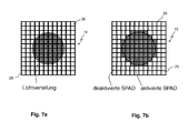
- Fig. 7 shows the same arrangement as in Fig. 6 but with a smaller light spot, resulting in a smaller pinhole size.
- Fig. 7a shows the basic light distribution and Fig. 7b the ratio of activated to deactivated SPADs 26.
- Fig. 8 shows as shown Fig. 5 on the one hand, the basic arrangement in a so-called SP detector with variable aperture, wherein in Fig. 8a the conventional application of photomultipliers 36 is indicated while Fig. 8b shows the use of arrangements of SPADs 26, namely SiPMs 19, which in turn may be equipped with and without microlenses.
- the detection light 37 passes through an optic 33 and a prism 39, split accordingly - via variable gap or pinhole apertures 40 - and beam splitter to the photomultipliers 36th According to Fig. 8b
- the photomultipliers are replaced by arrays of SPADs 26, namely, arrays of SiPMs 19.
- Fig. 9a shows the state of the art in so far as there photomultiplier 36 are used in variable gap or orifice plates 40. According to Fig. 9b these are replaced by an array 19 of SPADs 26.
- the detection light 37 accordingly passes through an optical system 33 and a prism 39 to the array (SiPM) consisting of individual SPADs 26.
- Fig. 10a again shows the light distribution.
- Fig. 10b is indicated by the indicated circle, the activation and deactivation of individual SPADs 26.
- Fig. 10 shows an array of SPADs for the detection of a first detection wavelength in the context of an application Fig. 8 ,
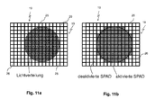
- Fig. 11 shows a corresponding arrangement of SPADs 26, namely, on the one hand the light distribution and on the other hand, the activation and deactivation of individual SPADs 26, but with respect to a second detection wavelength in the context of use in an SP detector as shown in FIG Fig. 8 ,
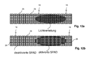
- FIG. 12 shows the structure of an array of SiPMs 19, each SiPM in turn comprising a plurality of SPADs 26.
- Fig. 12a shows in concrete terms the light distribution at corresponding spot in the context of a spectrometer as in Fig. 9b shown.
- Fig. 12b shows the deactivation and activation of a SPAD according to the light distribution.
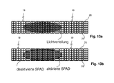
- FIG. 12 shows a structure of an array of SiPMs 19 accordingly Fig. 12 but with a different light distribution resulting from a different wavelength, for example the fluorescence light.
- Fig. 14 is of the fundamental structure as in the Fig. 12 and 13 , wherein the light distribution of the fluorescent light is in turn different. As shown in Fig. 14a the arrangement of the SiPMs 19 is applied to the illuminating light 41 of interest for evaluation and to stray light. Individual SPADs 26 are deactivated on the one hand because of the stray light and on the other hand due to a lack of illumination. The activated SPADs 26 are used for evaluation.
- the wavelength range in the spectrometer is deactivated at which unwanted stray light, for example reflection or scattered light of the excitation laser wavelengths, impinges. If necessary, adjacent areas are deactivated, namely due to so-called crosstalk.
- the deactivation of these areas is particularly important because the stray light is usually much stronger than the useful light (fluorescent light). Since the light distribution of the useful light depends on the fluorophores used by the user, all SPADs or pixels are activated on which no excitation light is incident (unless they are defect or dark noise pixels as described above), so that irrespective of the fluorophores used can be detected. A disturbance of excitation light is excluded. Likewise, with several Laser lines are stimulated simultaneously, then correspondingly more areas are hidden.
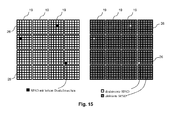
- Fig. 15 shows the arrangement of several SiPMs in the sense of a matrix-like array 19, wherein each SiPM 19 consists of several SPADs 26. Defective or insufficiently well working SPADs 26 causing high dark noise are disabled.
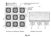
- Fig. 16 Finally, the arrangement of several SiPMs 19, each consisting of several SPADs 26, on a chip. Due to the unusable intermediate regions 43, the arrays of SiPMs 19 are associated with 19 microlenses 44, which in Fig. 16 are shown in side view. By using the microlenses 44 results in a more favorable light distribution, each focused on the usable areas of the SiPMs 19th
- FIG. 16 Also shows Fig. 16 the disabled SPADs that do not receive detection light.
Landscapes
- Physics & Mathematics (AREA)
- Spectroscopy & Molecular Physics (AREA)
- General Physics & Mathematics (AREA)
- Chemical & Material Sciences (AREA)
- Analytical Chemistry (AREA)
- Engineering & Computer Science (AREA)
- General Engineering & Computer Science (AREA)
- Optics & Photonics (AREA)
- Computer Vision & Pattern Recognition (AREA)
- Light Receiving Elements (AREA)
- Spectrometry And Color Measurement (AREA)
- Photometry And Measurement Of Optical Pulse Characteristics (AREA)
- Microscoopes, Condenser (AREA)
Abstract
Description
- Die Erfindung betrifft eine Vorrichtung zum Detektieren von Licht, insbesondere zur Anwendung in einem Mikroskop, in einem Spektrometer oder in einer Kamera. Des Weiteren betrifft die Erfindung ein entsprechendes Verfahren, vorzugsweise unter Nutzung der Vorrichtung.
- Die Erfindung beschäftigt sich ganz allgemein mit dem Detektieren von Licht, beispielsweise zur Anwendung in einem Mikroskop, in einem Spektrometer oder in einer Kamera. Die beanspruchte Vorrichtung ist nicht anwendungsgebunden. Sie ist im weitesten Sinne als Detektor für Licht zu verstehen.
- Aus der Praxis sind seit vielen Jahren Photomultiplier (PMT) bekannt, wobei es sich dabei um spezielle Elektronenröhren handelt, mit der Aufgabe, schwache Lichtsignale bis hin zu einzelnen Photonen durch Erzeugung und Verstärkung eines elektrischen Signals zu detektieren. Typischerweise besteht ein Photomultiplier aus einer Photokathode und einem nachgeschalteten Sekundärelektronenvervielfacher, angeordnet in einem evakuierten Glaskolben. Da es sich bei dem Photomultiplier um ein Röhrengerät handelt, baut dieser relativ groß, eignet sich daher nicht zur Miniaturisierung.
- Des Weiteren sind aus der Praxis Avalanche-Photodioden bzw. Lawinenphotodioden (APD) bekannt, wobei es sich dabei um hochempfindliche und schnelle Photodioden handelt. Sie nutzen den inneren photoelektrischen Effekt zur Ladungsträgererzeugung und den Lawinendurchbruch (Avalanche-Effekt) zur internen Verstärkung. APDs werden als das Halbleiteräquivalent zu Photomultipliern betrachtet und finden u.a. Anwendung bei der Detektierung sehr geringer Strahlungsleistungen mit Grenzfrequenzen bis in den Gigahertz-Bereich.
- Zur Photonenzählung werden APDs im Geiger-Modus betrieben, wobei man dabei regelmäßig von Single Photonen Avalanche Dioden (SPAD) spricht. Als neuere Entwicklungen sind Silicon-Photomultiplier (SiPM) bekannt, bei denen mehrere SPADs miteinander zu einer größeren Detektionsfläche analog oder digital kombiniert sind. Lediglich beispielhaft sei dazu auf die
US 2010/0214654 A1 verwiesen. - Bei der Auswahl der Detektionssysteme geht es regelmäßig um eine möglichst große Photonendetektionswahrscheinlichkeit (PDE), ein möglichst geringes Dunkelrauschen (hervorgerufen durch einen sogenannten Dunkelstrom einzelner lichtempfindlicher Elemente) und eine möglichst große bzw. maximale Photonenrate, d.h. um eine große Dynamik des Detektors.
- Photomultiplier-Röhren sind in der Konstruktion aufwändiger als Detektoren, die mit Si-Technologie gefertigt werden. Außerdem haben Photomultiplier in der Regel eine geringere Photonendetektionswahrscheinlichkeit als beispielsweise Avalanche-Photodioden. Bei sämtlichen Detektortypen hängt das Dunkelrauschen maßgeblich von der gesamten Detektionsfläche, der Qualität des Photokathodenmaterials sowie von der Betriebstemperatur des Detektors ab.
- Der vorliegenden Erfindung liegt die Aufgabe zu Grunde, eine Vorrichtung zum Detektieren von Licht und ein entsprechendes Verfahren anzugeben, wonach bei gegebener Beleuchtungs-/Lichtstärke eine hohe Bildqualität bzw. ein möglichst hohes Signal-Rauschverhältnis realisierbar ist. Die Vorrichtung soll möglichst klein bauen und kostengünstig in der Herstellung sein. Entsprechend ausgestattete Mikroskope, Spektrometer oder Kameras sollen angegeben werden.
- Voranstehende Aufgabe ist in Bezug auf die erfindungsgemäße Vorrichtung durch die Merkmale der nebengeordneten Patentansprüche 1 und 4 gelöst. In Bezug auf das erfindungsgemäße Verfahren ist die Aufgabe durch die Merkmale des nebengeordneten Patentanspruchs 16 gelöst. Mit den weiter nebengeordneten Patentansprüchen 13, 14 und 15 sind entsprechend ausgestattete Mikroskope, Spektrometer und Kameras beansprucht.
- Erfindungsgemäß ist die Vorrichtung zum Detektieren von Licht, insbesondere in einem Mikroskop, in einem Spektrometer oder in einer Kamera, mit mindestens einem Silicon-Photomultiplier (SiPM) ausgestattet. Der Silicon-Photomultiplier besteht aus einer Anordnung bzw. einem Array mehrerer Single Photonen Avalanche Dioden (SPAD). Erfindungswesentlich ist dabei, dass das Array eine größere Fläche als das auftreffende Licht hat, wobei nur diejenigen SPADs aktiviert und/oder ausgewertet werden, die mit einer bestimmten - hohen -Mindestintensität von Licht auch tatsächlich beaufschlagt bzw. getroffen werden.
- Erfindungsgemäß umfasst die Vorrichtung einen speziell angepassten SiPM, wobei der Aufbau des SiPM eine hohe Photonendetektionswahrscheinlichkeit (PDE) aufweist, nämlich wie bei den Single Photonen Avalanche Dioden (SPAD). Die Dynamik eines einzelnen Pixels ergibt sich aus der Anzahl der pro Pixel kombinierten SPADs sowie aus der Totzeit einer einzelnen SPAD. Die Totzeit kann mittels "active quenching" sehr kurz gehalten werden, nämlich im Bereich > 100 SPAD pro Pixel und < 50 ns Totzeit.
- Die hier verwendeten SiPM bieten die Möglichkeit, einzelne SPADs eines Pixels gezielt zu aktivieren bzw. zu deaktivieren. Dazu eignet sich insbesondere ein SiPM mit digitaler Auswertelektronik. So kann ein adressierbarer statischer Speicher dazu benutzt werden, einzelne SPADs direkt auf einem Chip - selektiv - zu aktivieren.
- Des Weiteren ist von ganz besonderem Vorteil, dass SiPMs in einem konventionellen CMOS-Prozess herstellbar sind. Entsprechend sind solche Silicon-Photomultiplier äußerst robust, insbesondere gegenüber hohen bzw. zu hohen Lichtleistungen.
- In vorteilhafter Weise umfasst die erfindungsgemäße Vorrichtung mehrere Silicon-Photomultiplier, jeweils bestehend aus einem Array mehrerer Single Photonen Avalanche Dioden. Die mehreren SiPMs können matrixartig, beispielsweise zur Anwendung in einer Kamera, oder linear nebeneinander, beispielsweise zur Anwendung in einem Spektrometer, angeordnet sein. Entsprechend der erfindungsgemäßen Lehre weist die Anordnung der SiPMs insgesamt eine größere Fläche als das auftreffende Licht auf, wobei nur diejenigen SPADs der verschiedenen SiPMs innerhalb der Anordnung aktiviert und/oder ausgewertet werden, die mit einer bestimmten - hohen - Mindestintensität von Licht beaufschlagt bzw. beleuchtet werden.
- Für die erfindungsgemäße Lehre ist wesentlich, dass die Vorrichtung einen einzigen Silicon-Photomultiplier mit einem Array aus SPADs oder eine Anordnung mehrerer SiPMs, jeweils mit einem Array aus SPADs, umfassen kann.
- Die Mindestintensität von Licht lässt sich aus einer oder mehreren Probemessungen bzw. einer Kalibrierung bei jeweils vorgegebener Systemeinstellung ermitteln.
- Nach der erfindungsgemäßen Lehre geht es grundsätzlich darum, das Dunkelrauschen der Vorrichtung bzw. eines entsprechend aufgebauten Detektors zu minimieren, indem nur diejenigen SPADs aktiviert werden, die zu einem hohen Signal-Rausch-Verhältnis beitragen. Folglich werden nur diejenigen SPADs bzw. Pixel aktiviert, auf denen auch tatsächlich Detektionslicht erwartet wird. Entsprechend liefern auch nur diese - aktivierten - SPADs einen Beitrag zum Dunkelrauschen.
- Des Weiteren ist - unabhängig von der voranstehend erwähnten Problematik - in weiter erfindungsgemäßer Weise erkannt worden, dass das Dunkelrauschen in ganz besonderem Maße von Defekten in der lichtempfindlichen Schicht der SPADs verursacht wird. So kommt es beispielsweise vor, dass eine schadhafte SPAD ein elektronisches Signal liefert, wenngleich kein Licht auf den lichtempfindlichen Bereich der Diode aufgetroffen ist. Die Wahrscheinlichkeit für ein solches Fehlverhalten wird Dunkelzählrate genannt, die es so gering wie möglich zu halten gilt.
- Da sich die zuvor erwähnten - größeren - Detektorflächen nicht völlig defektfrei herstellen lassen, sind bei SiPMs einige wenige, nicht ordnungsgemäß arbeitende SPADs (regelmäßig weniger als 5 %) vorhanden, die - ungeachtet ihrer geringen Anzahl - auf Grund einer nicht unerheblichen Dunkelzählrate für den Hauptanteil des Dunkelrauschens verantwortlich sind. Insoweit betrifft die erfindungsgemäße Lehre auch eine Vorrichtung zum Detektieren von Licht, insbesondere zur Anwendung in einem Mikroskop, in einem Spektrometer oder in einer Kamera, mit mindestens einem Silicon-Photomultiplier (SiPM), der aus einer Anordnung (Array) mehrerer Single Photonen Avalanche Dioden (SPAD) besteht, wobei je SiPM diejenigen SPADs deaktiviert oder nicht ausgewertet werden, deren Funktion unzureichend bzw. fehlerhaft ist, die somit nicht einwandfrei "performen". So ist in weiter erfindungsgemäßer Weise erkannt worden, dass durch Deaktivieren einzelner SPADs mit hohem Dunkelrauschen sich das Signal-Rausch-Verhältnis der gesamten Anordnung erheblich verbessert, auch wenn man auf das jeweilige Detektionssignal der fehlerhaften und somit in erfindungsgemäßer Weise deaktivierte SPAD verzichtet.
- Die unzureichende oder fehlerhafte Funktion einzelner SPADs lässt sich durch einen unteren Schwellwert des Verhältnisses von Nutzsignal zu Dunkelrauschen vorgeben, wobei es hier nicht auf einen festen Schwellwert ankommt.
- Die unzureichend ausgeleuchteten oder unzureichend oder fehlerhaft arbeitenden SPADs lassen sich durch Probe-/Kalibriermessungen ermitteln, so dass über die gesamte Betriebsdauer des SiPM hinweg eine Deaktivierung der fehlerhaften SPADs möglich ist. Dabei ist es weiter möglich, eine Art Beleuchtungsintensitätskarte bzw. Dunkelrauschkarte des Chips zu erstellen, wobei dazu zum Beispiel sequentiell jeweils nur ein Teil der SPADs pro Pixel und bevorzugt nur eine SPAD pro Pixel auf einmal aktiviert wird, so dass anhand der Pixelzählrate die Dunkelzählrate den einzelnen SPADs zugeordnet werden kann. Um den flächenmäßigen Anteil der zu deaktivierenden Pixel möglichst klein zu halten, kann es von Vorteil sein, möglichst viele kleine SPADs anstelle weniger großer SPADs pro Pixel zu verwenden.
- Grundsätzlich ist es denkbar, dass die zu deaktivierenden SPADs schlichtweg "abgeklemmt" werden, so dass diese innerhalb der gesamten Anordnung des SiPM keine Funktion haben.
- Auch ist es denkbar, dass die zu deaktivierenden SPADs über eine Steuerung, vorzugsweise progammiertechnisch, deaktiviert werden, so dass kein mechanischer Eingriff in die Anordnung erforderlich ist.
- Schließlich ist es auch denkbar, dass die elektrischen Ausgangssignale der nicht zu berücksichtigenden SPADs bei der Auswertung der Signale verworfen werden. An dieser Stelle sei angemerkt, dass die voranstehend genannten Methoden zur Deaktivierung bzw. zur Nicht-Berücksichtigung sowohl in Bezug auf die ermittelte Mindestintensität des Lichts als auch in Bezug auf fehlerhafte SPADs Anwendung finden können.
- In Bezug auf die Anordnung der einzelnen SPADs zur Bildung eines SiPM ist problematisch, dass auf Grund fertigungstechnischer Zwänge zwischen den einzelnen SPADs und vor allem auch zwischen den einzelnen Pixeln lichtunempfindliche Bereiche vorhanden sind, nämlich Randbereiche der SPADs und Zwischenräume zwischen den SPADs. Entsprechend ist der lichtempfindliche Anteil der gesamten beleuchteten Fläche, Füllfaktor genannt, erheblich geringer als 100 %, typischerweise im Bereich zwischen 50 % und 70 %. Daraus resultiert eine geringere Photonendetektionswahrscheinlichkeit, nämlich auf Grund der lichtunempfindlichen Bereiche. Um die damit einhergehende geringe Photonendetektionswahrscheinlichkeit im Vergleich zu einer einzelnen Single Photonen Avalanche Diode zu kompensieren, lassen sich in ganz besonders vorteilhafter Weise den SPADs eines SiPM Mikrolinsen bzw. ein auf die Anordnung der SPADs abgestimmtes Mikrolinsenarray zuordnen. Die Mikrolinsen fokussieren das auf die gesamte Anordnung auftreffende Licht auf die jeweils lichtempfindlichen Bereiche der SPADs, so dass sich durch diese Maßnahme der Füllfaktor erhöhen lässt. Je nach Geometrie des auftreffenden Lichts kann es bei gegebener SiPM-Geometrie auch sinnvoll sein, einzelne SPADs, die von dem fokussierten Licht nicht mehr getroffen würden, zu deaktivieren, und zwar ungeachtet der Vorkehrungen von Mikrolinsen.
- Insbesondere im Hinblick auf eine einfache Herstellung und kompakte Bauweise eines SiPM lassen sich dazu die SPADs auf einem Chip, vorzugsweise aus einem Silizium-Substrat, anordnen. Zur Reduzierung der Dunkelzählrate ist es möglich, den SiPM-Chip zu kühlen, beispielsweise mittels thermoselektiver Kühlung. Eine Kühlung unter -40° C ist möglich und von Vorteil.
- Eine Anwendung der erfindungsgemäßen Vorrichtung in konfokalen Mikroskopen ist von besonderem Vorteil, wobei dort, beispielsweise von einer Probe kommendes Fluoreszenz-Licht spektral selektiv zu detektieren ist. Hier bietet es sich an, die erfindungsgemäße Vorrichtung im Sinne eines Detektor-Arrays auszulegen.
- Auch lässt sich die erfindungsgemäße Vorrichtung in einem Spektrometer verwenden, wobei im Rahmen einer solchen Anwendung bekannt ist, welche Diode zu dem jeweils gewünschten Spektralbereich gehört. Entsprechend lassen sich nur diejenigen Pixel aktivieren, auf denen auch tatsächlich Detektionslicht im jeweiligen Spektralbereich erwartet wird.
- Auch die Verwendung der erfindungsgemäßen Vorrichtung in einer Kamera ist möglich, nämlich auf Grund der zuvor bereits genannten Eigenschaften einer Anordnung von SiPMs, jeweils bestehend aus Arrays einzelner SPADs.
- Zu den Merkmalen des erfindungsgemäßen Verfahrens sei zur Vermeidung von Wiederholungen auf die Ausführungen zu der erfindungsgemäßen Vorrichtung verwiesen, aus denen sich die das Verfahren betreffenden Merkmale ergeben. Auch hier ist wesentlich, dass nur diejenigen SPADs aktiviert und/oder ausgewertet werden, die mit einer bestimmten Mindestintensität von Licht auch tatsächlich beaufschlagt werden. Je SiPM werden - alternativ oder ergänzend - diejenigen SPADs aktiviert oder nicht ausgewertet, deren Funktion unzureichend bzw. fehlerhaft ist, die jedenfalls keine saubere Performance aufweisen.
- Es gibt nun verschiedene Möglichkeiten, die Lehre der vorliegenden Erfindung in vorteilhafter Weise auszugestalten und weiterzubilden. Dazu ist einerseits auf die den Hauptansprüchen nachgeordneten Patentansprüche und andererseits auf die nachfolgende Erläuterung bevorzugter Ausführungsbeispiele der Erfindung anhand der Zeichnung zu verweisen. In Verbindung mit der Erläuterung der bevorzugten Ausführungsbeispiele der Erfindung anhand der Zeichnung werden auch im Allgemeinen bevorzugte Ausgestaltungen und Weiterbildungen der Lehre erläutert. In der Zeichnung zeigen
- Fig. 1
- in einer schematischen Ansicht die grundsätzliche Anordnung eines konfokalen Mikroskops mit den wesentlichen Bauteilen, wobei eine erfindungsgemäße Vorrichtung als Detektor-Array ausgelegt ist,
- Fig. 2
- in einer schematischen Ansicht den grundsätzlichen Aufbau eines erfindungsgemäßen Arrays mit SPADs und deren Möglichkeit zur analogen oder digitalen Verschaltung/Auswertung,
- Fig. 3
- in einer schematischen Ansicht den grundsätzlichen Aufbau eines Spektrometers mit einer erfindungsgemäßen Vorrichtung als Detektor-Array,
- Fig. 4
- in schematischen Ansichten Anordnungen mehrerer SiPMs als Multipixel-SiPMs, beispielsweise zur Anwendung in einer Kamera (
Fig. 4a ) oder in einem Spektrometer (Fig. 4b ), - Fig. 5
- in schematischen Ansichten den Einsatz von SPAD-Anordnungen (Arrays) als Ersatz herkömmlicher Photomultiplier,
- Fig. 6
- in schematischen Ansichten die Lichtverteilung (
Fig. 6a ) und die Aktivierung/Deaktivierung einzelner SPADs (Fig. 6b ), - Fig. 7
- in schematischen Ansichten die Lichtverteilung (
Fig. 7a ) und die Aktivierung/Deaktivierung einzelner SPADs (Fig. 7b ), gegenüber der Darstellung inFig. 6 mit einem kleineren Lichtspot, - Fig. 8
- in schematischen Ansichten den Einsatz von SPAD-Anordnungen (Arrays) als Ersatz herkömmlicher Photomultiplier bei sogenannten SP-Detektoren mit variabler Blende,
- Fig. 9
- in schematischen Ansichten den Einsatz von SPAD-Anordnungen (Arrays) als Ersatz herkömmlicher Photomultiplier bei sogenannten SP-Detektoren mit variabler Blende, wobei die im Stand der Technik verwendeten Photomultiplier durch ein Array aus SPADs ersetzt ist
- Fig. 10
- in schematischen Ansichten die Lichtverteilung (
Fig. 10a ) und die Aktivierung/Deaktivierung einzelner SPADs (Fig. 10b ), - Fig. 11
- in schematischen Ansichten die Lichtverteilung (
Fig. 11a ) und die Aktivierung/Deaktivierung einzelner SPADs (Fig. 11b ), im Vergleich zu der Darstellung inFig. 10 in Bezug auf eine andere Detektionswellenlänge, - Fig. 12
- in einer schematischen Ansicht den Aufbau eines Arrays aus SiPMs, wobei
Fig. 12a die Lichtverteilung undFig. 12b die Aktivierung/Deaktivierung einzelner SPADs zeigt, - Fig. 13
- in einer schematischen Ansicht den Aufbau eines Arrays aus SiPMs, wobei
Fig. 13a die Lichtverteilung undFig. 13b die Aktivierung/Deaktivierung einzelner SPADs zeigt, jedoch in Bezug auf eine andere Wellenlänge, - Fig. 14
- in einer schematischen Ansicht die Lichtverteilung (
Fig. 14a ) und die Deaktivierung/Aktivierung einzelner SPADs (Fig. 14b ), wobei die SiPMs linear angeordnet sind, - Fig. 15
- in einer schematischen Ansicht die matrixartige Anordnung mehrerer SiPMs mit integrierten SPADs, wobei dort SPADs mit hohem Dunkelrauschen deaktiviert sind (
Fig. 15b ), - Fig. 16
- in einer schematischen Ansicht matrixartig angeordnete SiPMs, wobei dort zur Begünstigung der Lichtverteilung Mikrolinsen vorgesehen sind.
-
Fig. 1 zeigt am Beispiel eines konfokalen Scanmikroskops die Nutzung einer erfindungsgemäßen Vorrichtung zur Detektion von der Probe zurückkommenden Lichts. Im Konkreten zeigtFig. 1 den schematischen Aufbau eines konfokalen Scanmikroskops 1, bei dem ein Array 19 aus SPADs 26 zur Detektion der Signale vom Scanmikroskop 1 genutzt wird. Der von einer Lichtquelle 2 kommende Beleuchtungslichtstrahl 3 wird von einem Strahlteiler oder einem geeigneten Umlenkmittel 5 zu einer Scaneinrichtung 7 geleitet. Bevor der Beleuchtungslichtstrahl 3 auf das Umlenkmittel 5 trifft, passiert dieser ein Beleuchtungspinhole 6. - Die Scaneinrichtung 7 umfasst einen - bei diesem Beispiel - kardanisch aufgehängten Scanspiegel 9, der den Beleuchtungslichtstrahl 3 durch eine Scanoptik 12 und eine Mikroskopoptik 13 hindurch über bzw. durch ein Objekt 15 führt. Der Beleuchtungslichtstrahl 3 wird bei nicht transparenten Objekten 15 über die Objektoberfläche geführt. Bei biologischen bzw. transparenten Objekten 15 kann der Beleuchtungslichtstrahl 3 durch das Objekt geführt werden. Zu diesen Zwecken werden nichtleuchtende Präparate ggf. mit einem geeigneten Farbstoff präpariert.
- Die in dem Objekt 15 ggf. vorhandenen Farbstoffe werden durch den Beleuchtungslichtstrahl 3 angeregt und senden Licht in einem ihnen eigenen charakteristischen Bereich des Spektrums aus. Das vom Objekt 15 ausgehende Licht definiert einen Detektionslichtstrahl 17. Dieser gelangt durch die Mikroskopoptik 13, die Scanoptik 12 und über das Scanmodul 7 zum Umlenkmittel 5, passiert dieses und gelangt über eine Detektionslochblende 18 auf das Array 19. Der vom Objekt 15 ausgehende bzw. definierte Detektionslichtstrahl 17 ist in
Fig. 1 als gestrichelte Linie dargestellt. - Im Array 19 werden elektrische Detektionssignale erzeugt, die von der Leistung des vom Objekt 15 ausgehenden Lichts abhängen. Da vom Objekt 15 Licht nicht nur einer Wellenlänge ausgesandt wird, kann es sinnvoll sein, vor dem Array 19 ein dispersives Element 20 anzuordnen. Das dispersive Element 20 spaltet den Detektionslichtstrahl 17 spektral auf, so dass die einzelnen Wellenlängen des Detektionslichts räumlich spektral getrennt sind. Dem dispersiven Element 20 kann eine Linse 21 vorgeschaltet sein, die den Detektionslichtstrahl 17 aufweitet und parallelisiert. Dem dispersiven Element 20 kann außerdem eine Detektoroptik 22 nachgeschaltet sein, die die spektral getrennten Strahlen 24, 25 des Detektionslichtstrahl 17 auf das Array 19 fokussiert. Die spektral getrennten Strahlen 24, 25 unterscheiden sich hinsichtlich der Wellenlänge und treffen somit auf unterschiedliche Bereiche auf dem Array 19. In der hier dargestellten Ausführungsform ist vor dem dispersiven Element 20 eine Aufweitungsoptik 23 vorgesehen Die Aufweitungsoptik 23 kann derart ausgebildet sein, dass die numerische Apertur der Detektoroptik 22 unabhängig von der numerischen Apertur des Detektionslichtstrahls 17 an der Detektionslochblende 18 ist.
-
Fig. 2 zeigt in einer schematischen Ansicht den grundsätzlichen Aufbau eines Arrays 19 einer erfindungsgemäßen Vorrichtung, wobei das Array 19 mehrere SPADs 26 umfasst. Gemeinsam bilden die SPADs 26 den SiPM 19, bei diesem Ausführungsbeispiel für ein Pixel. -
Fig. 2 zeigt darüber hinaus die grundsätzliche Verschaltung des SiPM 19 bzw. des SPADs 26 bei analoger Auswertung 27 und digitaler Auswertung 28, wobei im Rahmen der analogen Auswertung 27 das Signal einem AD-Wandler 29 und einer entsprechenden Auswertung zugeführt wird. Im Rahmen der digitalen Auswertung 28 werden die Signale einer digitalen Auswertelogik 30 (on chip read out) zugeführt. Die SPADs 26 sind dabei einzeln adressierbar. -
Fig 3 . zeigt einen grundsätzlichen Spektrometer-Aufbau, wobei das zu detektierende Licht nach einer Blende/Pinhole 32 über eine Optik 33 parallelisiert und durch ein dispersives Element, z.B. ein Prisma, Gitter 34 oder Hologramm spektral aufgespalten wird. Über eine weitere Optik 35 gelangt das spektral aufgespaltene Licht zu einem Detektor-Array 31, welches als Multipixel-Array mit mehreren SiPMs, bestehend aus SPADs, aufgebaut ist. -
Fig. 4 zeigt mögliche Anordnungen von SiPMs 19, jeweils bestehend aus Arrays von SPADs 26. Die Anordnung des SiPMs 19 kann beispielsweise zur Anwendung in einer Kamera matrixartig (Fig. 4a ) ausgebildet sein. Zur Anwendung in einem Spektrometer können die SiPMs 19 linear (Fig. 4b ) angeordnet sein. In beiden Fällen sind jeweils 16 Pixel dargestellt bzw. abgebildet. Andere Pixelzahlen und Pixelanordnungen sind im Lichte der Erfindung möglich. -
Fig. 5a zeigt den Einsatz herkömmlicher Photomultiplier 36, beispielsweise in der Konfokalmikroskopie, wobei dort das Detektionslicht 37 über verschiedene dichroitische Strahlteiler 38 zu den jeweiligen Photomultipliern 36 zur Detektion konkreter Spektralbereiche gelangt. -
Fig. 5b zeigt den Ersatz der konventionellen Photomultiplier durch Anordnungen von SPADs 26, wobei den SPADs 26 Mikrolinsen zugeordnet sein können. Auch hier gelangt das Detektionslicht über dichroitische Strahlteiler 38 zu Detektoren, in diesem Fallen zu den Anordnungen von SPADs 26, nämlich zu den verschiedenen SiPMs 19, die SPAD-Arrays umfassen. -
Fig. 6 zeigt in schematischer Ansicht die Anordnung von SPADs 26, die gemeinsam ein SiPM 19 bilden. Im Konkreten ist inFig. 6a die Lichtverteilung angedeutet. Die SPADs 26 können einen Abstand (Subpixelabstand) von 50 µm x 50 µm aufweisen, wobei die Pixelgröße etwas kleiner ist, nämlich auf Grund des Zwischenabstands zwischen den Pixeln. Die photosensitive Fläche kann beispielsweise 40 x 40 Subpixel betragen, wobei dies der Größe einer photosensitiven Fläche im Bereich von 2 mm x 2 mm entspricht. - In
Fig. 6b ist angedeutet, welche SPADs 26 entsprechend der erfindungsgemäßen Lehre aktiviert bzw. deaktiviert sind. Die innerhalb des angedeuteten Kreises befindlichen SPADs 26 und die von der Kreislinie geschnittenen SPADs 26 sind aktiviert. Die außerhalb bzw. nicht in Berührung zu dem im Kreis befindlichen SPADs 26 sind deaktiviert, wie dies die erfindungsgemäße Lehre beansprucht. -
Fig. 7 zeigt die gleiche Anordnung wie inFig. 6 , jedoch mit einem kleineren Lichtspot, resultierend aus einer kleineren Pinhole-Größe.Fig. 7a zeigt die grundsätzliche Lichtverteilung undFig. 7b das Verhältnis von aktivierten zu deaktivierten SPADs 26. -
Fig. 8 zeigt entsprechend der Darstellung ausFig. 5 zum einen die grundsätzliche Anordnung bei einem sogenannten SP-Detektor mit variabler Blende, wobei inFig. 8a die herkömmliche Anwendung von Photomultipliern 36 angedeutet ist, währendFig. 8b den Einsatz von Anordnungen von SPADs 26, nämlich SiPMs 19, zeigt, wobei diese wiederum mit und ohne Mikrolinsen ausgestattet sein können. - Das Detektionslicht 37 gelangt über eine Optik 33 und ein Prisma 39, entsprechend aufgespalten - über variable Spalt- oder Lochblenden 40 - und Strahlteiler zu den Photomultipliern 36. Gemäß
Fig. 8b sind die Photomultiplier ersetzt durch Anordnungen von SPADs 26, nämlich durch Arrays von SiPMs 19. -
Fig. 9a zeigt den Stand der Technik insoweit, als dort Photomultiplier 36 bei variablen Spalt- oder Lochblenden 40 zum Einsatz kommen. GemäßFig. 9b sind diese durch ein Array 19 aus SPADs 26 ersetzt. Das Detektionslicht 37 gelangt entsprechend über eine Optik 33 und ein Prisma 39 zu dem Array (SiPM) bestehend aus einzelnen SPADs 26. - Die Anordnung aus SPADs entsprechend der Darstellung in
Fig. 8b ist im Detail inFig. 10 gezeigt, wobei dort die SPADs 26 - in ihrer Gesamtheit - ein 1-Pixel-SiPM 19 bilden. -
Fig. 10a zeigt hier wiederum die Lichtverteilung. InFig. 10b ist durch den angedeuteten Kreis die Aktivierung und Deaktivierung einzelner SPADs 26 angedeutet. - An dieser Stelle sei angemerkt, dass die in
Fig. 10 dargestellte Anordnung von SPADs 26 zum Ersatz einzelner Photomultiplier 36 dient, nämlich im Rahmen eines sogenannten SP-Detektors mit variabler Bandbreit des zu detektierenden Lichts.Fig. 10 zeigt dabei ein Array aus SPADs zur Detektion einer ersten Detektionswellenlänge im Rahmen einer Anwendung nachFig. 8 . -
Fig. 11 zeigt eine entsprechende Anordnung von SPADs 26, nämlich einerseits wiederum die Lichtverteilung und andererseits die Aktivierung und Deaktivierung einzelner SPADs 26, jedoch in Bezug auf eine zweite Detektionswellenlänge im Rahmen des Einsatzes bei einem SP-Detektor entsprechend der Darstellung inFig. 8 . -
Fig. 12 zeigt den Aufbau eines Arrays aus SiPMs 19, wobei jedes SiPM wiederum mehrere SPADs 26 umfasst.Fig. 12a zeigt im Konkreten die Lichtverteilung bei entsprechenden Spot im Rahmen eines Spektrometers wie inFig. 9b gezeigt.Fig. 12b zeigt die Deaktivierung und Aktivierung eines SPADs entsprechend der Lichtverteilung. -
Fig. 13 zeigt einen Aufbau eines Arrays aus SiPMs 19 entsprechendFig. 12 , jedoch mit einer anderen Lichtverteilung, resultierend aus einer anderen Wellenlänge, beispielsweise des Fluoreszenzlichts. -
Fig. 14 wird vom grundsätzlichen Aufbau wie in denFig. 12 und13 , wobei die Lichtverteilung des Fluoreszenzlichts wiederum anders ist. Entsprechend der Darstellung inFig. 14a wird die Anordnung der SiPMs 19 mit dem zur Auswertung interessierenden Beleuchtungslicht 41 und mit Störlicht beaufschlagt. Es werden einzelne SPADs 26 zum einen wegen des Störlichts und zum anderen auf Grund mangelnder Ausleuchtung deaktiviert. Die aktivierten SPADs 26 dienen zur Auswertung. - Bei der Anwendung in einem Spektrometer wird speziell der Wellenlängenbereich im Spektrometer deaktiviert, an dem unerwünschten Störlicht, beispielsweise Reflexions- oder Streulicht der Anregungs-Laserwellenlängen, auftrifft. Gegebenenfalls werden auch Nachbarbereiche deaktiviert, nämlich auf Grund von sogenanntem Übersprechen. Die Deaktivierung dieser Bereiche ist besonders wichtig, da das Störlicht in der Regel deutlich stärker als das Nutzlicht (Fluoreszenzlicht) ist. Da die Lichtverteilung des Nutzlichts von den vom Benutzer eingesetzten Fluorophoren abhängt, werden alle SPADs bzw. Pixel aktiviert, auf die kein Anregungslicht fällt (sofern es sich nicht um Defekt- bzw. Dunkelrauschpixel wie zuvor beschrieben handelt), so dass unabhängig von den eingesetzten Fluorophoren detektiert werden kann. Eine Störung von Anregungslicht ist ausgeschlossen. Ebenso kann mit mehreren Laserlinien gleichzeitig angeregt werden, wobei dann entsprechend mehrere Bereiche ausgeblendet werden.
- Im Rahmen der Darstellung von
Fig. 14 gibt es drei Gründe, einzelne SPADs bzw. Subpixel zu deaktivieren, nämlich nur dann, wenn zu wenig Beleuchtungslicht auf die SPADs bzw. Subpixel fällt, wenn einzelne SPADs bzw. Subpixel unzureichend bzw. schlecht arbeiten (Dunkelrauschen o.ä.) oder wenn auf die SPADs bzw. Subpixel Störlicht fällt. -
Fig. 15 zeigt die Anordnung mehrere SiPMs im Sinne eines matrixartigen Arrays 19, wobei jedes SiPM 19 aus mehreren SPADs 26 besteht. Defekte bzw. nicht hinreichend gut arbeitende SPADs 26, die ein hohes Dunkelrauschen verursachen, sind deaktiviert. -
Fig. 16 zeigt schließlich die Anordnung mehrerer SiPMs 19, jeweils bestehend aus mehreren SPADs 26, auf einem Chip. Auf Grund der nicht nutzbaren Zwischenbereiche 43 sind den Arrays von SiPMs 19 Mikrolinsen 44 zugeordnet, die inFig. 16 in Seitenansicht gezeigt sind. Unter Nutzung der Mikrolinsen 44 ergibt sich eine günstigere Lichtverteilung, jeweils fokussiert auf die nutzbaren Bereiche der SiPMs 19. - Außerdem zeigt
Fig. 16 die deaktivierten SPADs, auf die kein Detektionslicht fällt. - Hinsichtlich weiterer Merkmale, die sich den Figuren nicht entnehmen lassen, sei zur Vermeidung von Wiederholungen auf den allgemeinen Teil der Beschreibung sowie auf die beigefügten Patentansprüche verwiesen.
- Schließlich sei ausdrücklich darauf hingewiesen, dass die voranstehend beschriebenen Ausführungsbeispiele der erfindungsgemäßen Vorrichtung lediglich zur Erörterung der beanspruchten Lehre dienen, diese jedoch nicht auf die Ausführungsbeispiele einschränken.
-
- 1
- konfokales Scanmikroskop
- 2
- Lichtquelle
- 3
- Beleuchtungslichtstrahl
- 5
- Umlenkmittel
- 6
- Beleuchtungspinhole
- 7
- Scaneinrichtung
- 9
- Scanspielgel
- 12
- Scanoptik
- 13
- Mikroskopoptik
- 15
- Objekt
- 17
- Detektionslichtstrahl
- 18
- Detektionslochblende
- 19
- Array, SiPM
- 20
- dispersives Element
- 21
- Linse
- 22
- Detektoroptik
- 23
- Aufweitungsoptik
- 24
- Stahlen
- 25
- Strahlen
- 26
- SPAD
- 27
- analoge Auswertung
- 28
- digitale Auswertung
- 29
- AD-Wandler
- 30
- digitale Auswertelogik
- 31
- Detektor-Array
- 32
- Blende/Pinhole
- 33
- Optik
- 34
- Prisma/Gitter
- 35
- Optik
- 36
- Photomultiplier
- 37
- Detektionslicht
- 38
- dichroitischer Strahlteiler
- 39
- Prisma
- 40
- variable Lochblende
- 41
- Beleuchtungslicht
- 42
- Streulicht
- 43
- Zwischenbereich
- 44
- Mikrolinse
Claims (15)
- Vorrichtung zum Detektieren von Licht, insbesondere zur Anwendung in einem Mikroskop, einem Spektrometer oder einer Kamera, mit mindestens einem Silicon Photomultiplier (SiPM), der aus einer Anordnung (Array) mehrerer Single Photon Avalanche Dioden (SPAD) besteht, wobei das Array eine größere Fläche als das auftreffende Licht aufweist und wobei nur diejenigen SPADs aktiviert und/oder ausgewertet werden, die mit einer bestimmten Mindestintensität von Licht beaufschlagt werden.
- Vorrichtung nach Anspruch 1, dadurch gekennzeichnet, dass eine Anordnung mehrerer Silicon Photomultiplier (SiPM) vorgesehen ist, wobei jeder SiPM aus einem Array von Single Photon Avalanche Dioden (SPAD) besteht, wobei die Anordnung eine größere Fläche als das auftreffende Licht aufweist und wobei nur diejenigen SPADs innerhalb der Anordnung von SiPMs aktiviert und/oder ausgewertet werden, die mit einer bestimmten Mindestintensität von Licht beaufschlagt werden.
- Vorrichtung nach Anspruch 1 oder 2, dadurch gekennzeichnet, dass die Mindestintensität des Lichts aus einer oder mehreren Probemessungen bzw. einer Kalibrierung bei jeweils vorgegebener Systemeinstellung resultiert.
- Vorrichtung zum Detektieren von Licht, insbesondere zur Anwendung in einem Mikroskop, einem Spektrometer oder einer Kamera, mit mindestens einem Silicon Photomultiplier (SiPM), der aus einer Anordnung (Array) mehrerer Single Photon Avalanche Dioden (SPAD) besteht, insbesondere mit den Merkmalen der Ansprüche 1 bis 3, wobei je SiPM diejenigen SPADs deaktiviert oder nicht ausgewertet werden, deren Funktion unzureichend bzw. fehlerhaft ist, wobei die unzureichende oder fehlerhafte Funktion einzelner SPADs durch einen unteren Schwellwert des Verhältnisses von Nutzsignal zu Dunkelrauschen vorgebbar sein kann, und/oder wobei durch Probe-/Kalibriermessungen die unzureichend oder fehlerhaft arbeitenden SPADs ermittelbar, und über die Betriebsdauer des SiPM hinweg deaktivierbar sein können.
- Vorrichtung nach einem der Ansprüche 1 bis 4, dadurch gekennzeichnet, dass die zu deaktivierenden SPADs abgeklemmt werden oder über die Steuerung, vorzugsweise programmiertechnisch, deaktiviert werden.
- Verfahren nach einem der Ansprüche 1 bis 4, dadurch gekennzeichnet, dass die elektrischen Ausgangssignale der nicht zu berücksichtigenden SPADs bei der Auswertung der Signale verworfen werden.
- Vorrichtung nach einem der Ansprüche 1 bis 6, dadurch gekennzeichnet, dass den einzelnen SPADs eines SiPM Mikrolinsen bzw. ein auf die Anordnung der SPADs abgestimmtes Mikrolinsenarray zugeordnet sind/ist, die das Licht auf die lichtempfindlichen Bereiche der SPADs fokussieren.
- Vorrichtung nach einem der Ansprüche 1 bis 7, dadurch gekennzeichnet, dass die SPADs eines SiPM auf einem Chip, vorzugsweise aus einem Siliziumsubstrat, angeordnet sind, wobei der Chip vorzugsweise thermoelektrisch gekühlt sein kann.
- Mikroskop, insbesondere Konfokalmikroskop, gekennzeichnet durch eine Vorrichtung zur Detektion von der Probe zurückkehrenden Lichts nach einem der Ansprüche 1 bis 8.
- Spektrometer, gekennzeichnet durch eine Vorrichtung zur Detektion der Spektralbereiche von Licht nach einem der Ansprüche 1 bis 8.
- Kamera, gekennzeichnet durch eine Vorrichtung zur Aufnahme von Licht zur Bilderzeugung nach einem der Ansprüche 1 bis 8.
- Verfahren zum Detektieren von Licht, insbesondere zur Anwendung in einem Mikroskop, einem Spektrometer oder einer Kamera, vorzugsweise unter Nutzung einer Vorrichtung nach einem der Ansprüche 1 bis 8, mit mindestens einem Silicon Photomultiplier (SiPM), der aus einer Anordnung (Array) mehrerer Single Photon Avalanche Dioden (SPAD) besteht, wobei das Array eine größere Fläche als das auftreffende Licht aufweist und wobei nur diejenigen SPADs aktiviert und/oder ausgewertet werden, die mit einer bestimmten Mindestintensität von Licht beaufschlagt werden und/oder wobei je SiPM diejenigen SPADs deaktiviert oder nicht ausgewertet werden, deren Funktion unzureichend bzw. fehlerhaft ist.
- Verfahren nach Anspruch 12, dadurch gekennzeichnet, dass die Mindestintensität der Beaufschlagung mit Licht aus einer oder mehreren Probemessungen bzw. einer Kalibrierung bei vorgegebener Systemeinstellung resultiert.
- Verfahren nach Anspruch 12 oder 13, dadurch gekennzeichnet, dass durch Probe-/ Kalibriermessungen die unzureichend oder fehlerhaft arbeitenden SPADs ermittelt werden und über die gesamte Betriebsdauer des SiPM deaktiviert werden.
- Verfahren nach Anspruch 14, dadurch gekennzeichnet, dass zur Ermittlung unzureichender oder fehlerhafter SPADs vorzugsweise jedes einzelne SPAD je SiPM aktiviert wird und anhand der Pixelzählrate die Dunkelzählrate den einzelnen SPAD zugeordnet wird.
Applications Claiming Priority (1)
| Application Number | Priority Date | Filing Date | Title |
|---|---|---|---|
| DE102011107645A DE102011107645A1 (de) | 2011-07-12 | 2011-07-12 | Vorrichtung und Verfahren zum Detektieren von Licht |
Publications (2)
| Publication Number | Publication Date |
|---|---|
| EP2546621A1 true EP2546621A1 (de) | 2013-01-16 |
| EP2546621B1 EP2546621B1 (de) | 2021-10-06 |
Family
ID=46516542
Family Applications (1)
| Application Number | Title | Priority Date | Filing Date |
|---|---|---|---|
| EP12174314.0A Active EP2546621B1 (de) | 2011-07-12 | 2012-06-29 | Vorrichtung und Verfahren zum Detektieren von Licht |
Country Status (5)
| Country | Link |
|---|---|
| US (1) | US10101203B2 (de) |
| EP (1) | EP2546621B1 (de) |
| JP (1) | JP6420941B2 (de) |
| CN (1) | CN102879088B (de) |
| DE (1) | DE102011107645A1 (de) |
Cited By (7)
| Publication number | Priority date | Publication date | Assignee | Title |
|---|---|---|---|---|
| LU92664B1 (de) * | 2015-02-24 | 2016-08-25 | Leica Microsystems | Vorrichtung und verfahren zum detektieren von licht |
| LU92665B1 (de) * | 2015-02-24 | 2016-08-25 | Leica Microsystems | Verfahren zur verbesserung des dynamikbereichs einer vorrichtung zum detektieren von licht |
| CN107422392A (zh) * | 2017-08-08 | 2017-12-01 | 中国科学院西安光学精密机械研究所 | 一种基于单光子探测的绕角定位与追踪系统及方法 |
| WO2022043429A1 (en) * | 2020-08-28 | 2022-03-03 | Ams International Ag | Dynamic range extension of spad-based devices |
| WO2022043456A1 (en) * | 2020-08-28 | 2022-03-03 | Ams International Ag | Dynamic range extension of spad-based devices |
| WO2023057123A1 (de) * | 2021-10-08 | 2023-04-13 | Heidelberg Engineering Gmbh | Anordnung mit einem detektor |
| PL453524A1 (pl) * | 2025-10-21 | 2026-08-03 | Politechnika Warszawska | Układ pomiarowy do odczytu dozymetrów pasywnych z optycznie stymulowaną luminescencją oraz sposób odczytu dawki promieniowania |
Families Citing this family (101)
| Publication number | Priority date | Publication date | Assignee | Title |
|---|---|---|---|---|
| US20110095192A1 (en) * | 2009-10-26 | 2011-04-28 | Johnson Kurtis F | Method to increase dynamic range of segmented non-linear devices |
| JP2014139564A (ja) * | 2012-12-20 | 2014-07-31 | Sony Corp | 撮像装置および電子機器 |
| ITTO20130538A1 (it) * | 2013-06-28 | 2014-12-28 | St Microelectronics Srl | Sistema e metodo di misura di frequenza di oscillazione per un sensore mems e corrispondente sensore mems |
| GB201317968D0 (en) * | 2013-10-10 | 2013-11-27 | Univ Glasgow | Endoscopy capsule |
| DE102014207599B4 (de) * | 2014-04-23 | 2024-09-26 | Robert Bosch Gmbh | Verfahren und Computerprogramm zum Betreiben eines Fotodetektors |
| JP6408796B2 (ja) * | 2014-06-11 | 2018-10-17 | オリンパス株式会社 | レーザ顕微鏡装置 |
| JP6435154B2 (ja) | 2014-10-14 | 2018-12-05 | 株式会社ジョブ | 光子計数型検出器 |
| JP6657242B2 (ja) * | 2014-10-29 | 2020-03-04 | モレキュラー デバイシーズ, エルエルシー | 顕微鏡システムにおいて並行撮像を用いることにより合焦画像を生成するための装置および方法 |
| US9854231B2 (en) * | 2014-12-18 | 2017-12-26 | General Electric Company | Silicon photomultipliers with internal calibration circuitry |
| JP6333189B2 (ja) * | 2015-02-09 | 2018-05-30 | 三菱電機株式会社 | レーザ受信装置 |
| US9819144B2 (en) | 2015-05-14 | 2017-11-14 | Apple Inc. | High-efficiency vertical emitters with improved heat sinking |
| US10034375B2 (en) | 2015-05-21 | 2018-07-24 | Apple Inc. | Circuit substrate with embedded heat sink |
| CN105072358A (zh) * | 2015-06-04 | 2015-11-18 | 南京瑞派宁信息科技有限公司 | 一种少像素相机成像方法及装置 |
| US9735539B2 (en) | 2015-07-20 | 2017-08-15 | Apple Inc. | VCSEL structure with embedded heat sink |
| US10620300B2 (en) | 2015-08-20 | 2020-04-14 | Apple Inc. | SPAD array with gated histogram construction |
| US10324171B2 (en) | 2015-12-20 | 2019-06-18 | Apple Inc. | Light detection and ranging sensor |
| US9997551B2 (en) | 2015-12-20 | 2018-06-12 | Apple Inc. | Spad array with pixel-level bias control |
| CN108292579B (zh) | 2015-12-22 | 2019-12-20 | 株式会社日立高新技术 | 带电粒子束装置 |
| CN105628197A (zh) * | 2015-12-26 | 2016-06-01 | 武汉京邦科技有限公司 | 一种照度计 |
| DK3442911T3 (da) * | 2016-04-13 | 2022-06-07 | Emerging Compounds Treat Technologies Inc | Bæredygtigt system og fremgangsmåde til fjernelse og koncentration af per- og polyfluoralkylstoffer (pfas) fra vand |
| US9985071B2 (en) | 2016-04-15 | 2018-05-29 | Qualcomm Incorporated | Active area selection for LIDAR receivers |
| US10948344B2 (en) * | 2016-08-26 | 2021-03-16 | Halliburton Energy Services, Inc. | Optical fiber spectroscopy using single photon detectors (SPDs) |
| US10502830B2 (en) * | 2016-10-13 | 2019-12-10 | Waymo Llc | Limitation of noise on light detectors using an aperture |
| DE102016224162A1 (de) * | 2016-12-05 | 2018-06-07 | Continental Automotive Gmbh | Head-Up-Display |
| JP6639427B2 (ja) | 2017-01-13 | 2020-02-05 | 株式会社東芝 | 受光装置 |
| JP6929671B2 (ja) * | 2017-03-17 | 2021-09-01 | キヤノン株式会社 | 撮像装置及び撮像システム |
| JP6867212B2 (ja) * | 2017-03-31 | 2021-04-28 | 株式会社デンソー | 光検出器及び測距装置 |
| US10830879B2 (en) | 2017-06-29 | 2020-11-10 | Apple Inc. | Time-of-flight depth mapping with parallax compensation |
| EP3428574A1 (de) | 2017-07-11 | 2019-01-16 | Fondazione Bruno Kessler | Vorrichtung zur abstandsmessung und verfahren zur messung des abstands |
| KR101938984B1 (ko) | 2017-08-09 | 2019-04-10 | 연세대학교 산학협력단 | Spad 거리측정 센서 기반의 2단계 트래킹을 이용한 거리 측정 장치 및 방법 |
| US10955552B2 (en) | 2017-09-27 | 2021-03-23 | Apple Inc. | Waveform design for a LiDAR system with closely-spaced pulses |
| JP7096658B2 (ja) * | 2017-10-12 | 2022-07-06 | キヤノン株式会社 | 固体撮像素子及び撮像装置 |
| FR3073050B1 (fr) | 2017-11-02 | 2023-06-30 | Centre Nat Rech Scient | Appareil et procede de microscopie a fluorescence a super-resolution et de mesure de temps de vie de fluorescence |
| JP6929760B2 (ja) | 2017-11-07 | 2021-09-01 | キヤノン株式会社 | 電子線検出素子、電子顕微鏡、透過型電子顕微鏡 |
| JP6961465B2 (ja) * | 2017-11-07 | 2021-11-05 | キヤノン株式会社 | 電子線検出素子、電子顕微鏡、および、透過型電子顕微鏡 |
| KR102403544B1 (ko) | 2017-12-18 | 2022-05-30 | 애플 인크. | 방출기들의 어드레스가능 어레이를 사용하는 비행 시간 감지 |
| CN111758019B (zh) * | 2018-01-23 | 2024-06-28 | 贝克顿·迪金森公司 | 用于动态光检测遮蔽的系统及其使用方法 |
| CN108375417B (zh) * | 2018-02-28 | 2024-05-10 | 深圳市纽创信安科技开发有限公司 | 一种单光子检测设备 |
| JP6954228B2 (ja) * | 2018-05-22 | 2021-10-27 | 株式会社デンソー | 光検出器およびその制御方法 |
| JP6969504B2 (ja) * | 2018-06-08 | 2021-11-24 | 株式会社デンソー | 測距装置 |
| CO2018007716A1 (es) | 2018-07-25 | 2020-01-31 | Univ Antonio Narino | Receptor para señales ópticas de baja potencia con funcionamiento en condiciones de alta incidencia de luz de fondo y aplicación en comunicación con luz visible |
| EP3914950A1 (de) * | 2019-01-25 | 2021-12-01 | Carl Zeiss Microscopy GmbH | Lichtmikroskop mit photonenzählenden detektorelementen und abbildungsverfahren |
| WO2020167338A1 (en) | 2019-02-11 | 2020-08-20 | Apple Inc. | Depth sensing using a sparse array of pulsed beams |
| JP6949067B2 (ja) * | 2019-03-05 | 2021-10-13 | キヤノン株式会社 | 撮像素子及びその制御方法、撮像装置、及び、画像処理装置 |
| JP7095626B2 (ja) * | 2019-03-06 | 2022-07-05 | 株式会社デンソー | 光学的測距装置 |
| JP7273565B2 (ja) | 2019-03-19 | 2023-05-15 | 株式会社東芝 | 受光装置及び距離測定装置 |
| US11500094B2 (en) | 2019-06-10 | 2022-11-15 | Apple Inc. | Selection of pulse repetition intervals for sensing time of flight |
| WO2020261278A1 (en) * | 2019-06-25 | 2020-12-30 | 5D Sensing Ltd. | Digital readout enabling 2d and 3d analysis for silicon photo multiplier |
| US10881028B1 (en) | 2019-07-03 | 2020-12-29 | Apple Inc. | Efficient heat removal from electronic modules |
| US11555900B1 (en) | 2019-07-17 | 2023-01-17 | Apple Inc. | LiDAR system with enhanced area coverage |
| US11131781B2 (en) | 2019-09-20 | 2021-09-28 | Waymo Llc | Programmable SiPM arrays |
| US11733359B2 (en) * | 2019-12-03 | 2023-08-22 | Apple Inc. | Configurable array of single-photon detectors |
| CN112909033A (zh) | 2019-12-04 | 2021-06-04 | 半导体元件工业有限责任公司 | 半导体器件 |
| US11764314B2 (en) | 2019-12-04 | 2023-09-19 | Semiconductor Components Industries, Llc | Scattering structures for single-photon avalanche diodes |
| CN112909034A (zh) | 2019-12-04 | 2021-06-04 | 半导体元件工业有限责任公司 | 半导体器件 |
| CN112909032A (zh) | 2019-12-04 | 2021-06-04 | 半导体元件工业有限责任公司 | 半导体器件 |
| CN112909031A (zh) | 2019-12-04 | 2021-06-04 | 半导体元件工业有限责任公司 | 半导体器件 |
| CN113132581A (zh) * | 2019-12-31 | 2021-07-16 | 深圳市灵明光子科技有限公司 | 成像方法、成像装置和电子设备 |
| KR20210087349A (ko) | 2020-01-02 | 2021-07-12 | 삼성전자주식회사 | 라이다 장치 및 그 동작 방법 |
| US11953625B2 (en) * | 2020-01-27 | 2024-04-09 | The Charles Stark Draper Laboratory, Inc. | Beamsplitter architecture for monostatic LiDAR |
| US11646335B2 (en) | 2020-01-30 | 2023-05-09 | Semiconductor Components Industries, Llc | Semiconductor devices with single-photon avalanche diodes and rectangular microlenses |
| US11969259B2 (en) | 2020-02-21 | 2024-04-30 | Hi Llc | Detector assemblies for a wearable module of an optical measurement system and including spring-loaded light-receiving members |
| WO2021167893A1 (en) | 2020-02-21 | 2021-08-26 | Hi Llc | Integrated detector assemblies for a wearable module of an optical measurement system |
| US11950879B2 (en) | 2020-02-21 | 2024-04-09 | Hi Llc | Estimation of source-detector separation in an optical measurement system |
| US11630310B2 (en) | 2020-02-21 | 2023-04-18 | Hi Llc | Wearable devices and wearable assemblies with adjustable positioning for use in an optical measurement system |
| US11883181B2 (en) | 2020-02-21 | 2024-01-30 | Hi Llc | Multimodal wearable measurement systems and methods |
| US12029558B2 (en) | 2020-02-21 | 2024-07-09 | Hi Llc | Time domain-based optical measurement systems and methods configured to measure absolute properties of tissue |
| US12144653B2 (en) | 2020-02-21 | 2024-11-19 | Hi Llc | Systems, circuits, and methods for reducing common-mode noise in biopotential recordings |
| WO2021188496A1 (en) * | 2020-03-20 | 2021-09-23 | Hi Llc | Photodetector calibration of an optical measurement system |
| US11187575B2 (en) | 2020-03-20 | 2021-11-30 | Hi Llc | High density optical measurement systems with minimal number of light sources |
| US11877825B2 (en) | 2020-03-20 | 2024-01-23 | Hi Llc | Device enumeration in an optical measurement system |
| US11864867B2 (en) | 2020-03-20 | 2024-01-09 | Hi Llc | Control circuit for a light source in an optical measurement system by applying voltage with a first polarity to start an emission of a light pulse and applying voltage with a second polarity to stop the emission of the light pulse |
| US11245404B2 (en) | 2020-03-20 | 2022-02-08 | Hi Llc | Phase lock loop circuit based signal generation in an optical measurement system |
| US12059262B2 (en) | 2020-03-20 | 2024-08-13 | Hi Llc | Maintaining consistent photodetector sensitivity in an optical measurement system |
| US11857348B2 (en) | 2020-03-20 | 2024-01-02 | Hi Llc | Techniques for determining a timing uncertainty of a component of an optical measurement system |
| US11645483B2 (en) | 2020-03-20 | 2023-05-09 | Hi Llc | Phase lock loop circuit based adjustment of a measurement time window in an optical measurement system |
| WO2021188488A1 (en) | 2020-03-20 | 2021-09-23 | Hi Llc | Bias voltage generation in an optical measurement system |
| WO2021188487A1 (en) | 2020-03-20 | 2021-09-23 | Hi Llc | Temporal resolution control for temporal point spread function generation in an optical measurement system |
| US11819311B2 (en) | 2020-03-20 | 2023-11-21 | Hi Llc | Maintaining consistent photodetector sensitivity in an optical measurement system |
| US12138068B2 (en) | 2020-03-20 | 2024-11-12 | Hi Llc | Techniques for characterizing a nonlinearity of a time-to-digital converter in an optical measurement system |
| US11876109B2 (en) | 2020-05-06 | 2024-01-16 | Semiconductor Components Industries, Llc | Semiconductor devices with single-photon avalanche diodes and light spreading lenses |
| US11710945B2 (en) | 2020-05-25 | 2023-07-25 | Apple Inc. | Projection of patterned and flood illumination |
| CN113916376B (zh) * | 2020-07-08 | 2025-07-08 | 高利通科技(深圳)有限公司 | 一种光谱仪控制方法及系统 |
| US11699715B1 (en) | 2020-09-06 | 2023-07-11 | Apple Inc. | Flip-chip mounting of optoelectronic chips |
| JP7423485B2 (ja) * | 2020-09-18 | 2024-01-29 | 株式会社東芝 | 距離計測装置 |
| JP7374937B2 (ja) | 2021-01-13 | 2023-11-07 | 株式会社アドバンテスト | 試験装置、試験方法およびプログラム |
| JP7386190B2 (ja) | 2021-01-21 | 2023-11-24 | 株式会社アドバンテスト | 試験装置、試験方法およびプログラム |
| US12442926B2 (en) | 2021-02-04 | 2025-10-14 | Apple Inc. | Time-of-flight depth sensing with improved linearity |
| CN113009292B (zh) * | 2021-02-25 | 2021-12-28 | 西安交通大学 | 局部放电微光光谱探测器 |
| JP7355773B2 (ja) | 2021-02-26 | 2023-10-03 | 株式会社アドバンテスト | 試験装置、試験方法およびプログラム |
| US12196860B2 (en) | 2021-03-02 | 2025-01-14 | Apple Inc. | Depth sensor calibration using internal reflections |
| US11681028B2 (en) | 2021-07-18 | 2023-06-20 | Apple Inc. | Close-range measurement of time of flight using parallax shift |
| JP7355789B2 (ja) | 2021-09-08 | 2023-10-03 | 株式会社アドバンテスト | 試験装置、試験方法およびプログラム |
| JP7862233B2 (ja) | 2022-06-13 | 2026-05-19 | 株式会社エビデント | レーザ走査型顕微鏡、画像処理装置、レーザ走査型顕微鏡の動作方法、及び、プログラム |
| US12313812B2 (en) | 2022-09-20 | 2025-05-27 | Apple Inc. | MOE-based illumination projector |
| US12663596B2 (en) | 2023-05-22 | 2026-06-23 | Apple Inc. | Pattern projector |
| US12123589B1 (en) | 2023-05-22 | 2024-10-22 | Apple Inc. | Flood projector with microlens array |
| DE102023206048A1 (de) | 2023-06-27 | 2025-01-02 | Carl Zeiss Microscopy Gmbh | Verfahren zur Korrektur von Messwerten eines optischen Detektionskanals |
| CN122029411A (zh) | 2023-10-16 | 2026-05-12 | 特里纳米克斯股份有限公司 | 用于评估光电检测器的劣化的方法 |
| EP4718138A1 (de) * | 2024-09-25 | 2026-04-01 | Leica Microsystems CMS GmbH | Detektionsanordnung, kaskadierte detektionsanordnung und optisches scanmikroskop |
| CN121855687B (zh) * | 2026-03-17 | 2026-07-17 | 江苏鲁德科技有限公司 | 光电探测装置和光学检测装置 |
Citations (3)
| Publication number | Priority date | Publication date | Assignee | Title |
|---|---|---|---|---|
| US20070182949A1 (en) * | 2005-12-21 | 2007-08-09 | Cristiano Niclass | Method and arrangement for measuring the distance to an object |
| DE102006013290A1 (de) * | 2006-03-23 | 2007-09-27 | Robert Bosch Gmbh | Vorrichtung zur optischen Distanzmessung sowie Verfahren zum Betrieb einer solchen Vorrichtung |
| US20100214654A1 (en) | 2007-05-22 | 2010-08-26 | Leica Microsystems Cms Gmbh | Apparatus for the detection of light in a scanning microscope |
Family Cites Families (11)
| Publication number | Priority date | Publication date | Assignee | Title |
|---|---|---|---|---|
| JP3315938B2 (ja) * | 1998-11-20 | 2002-08-19 | 理化学研究所 | 半導体暗像位置検出素子 |
| US6995841B2 (en) * | 2001-08-28 | 2006-02-07 | Rice University | Pulsed-multiline excitation for color-blind fluorescence detection |
| DE10332193A1 (de) * | 2003-07-15 | 2005-02-03 | Leica Microsystems Heidelberg Gmbh | Detektionsvorrichtung |
| US8077309B2 (en) * | 2007-01-29 | 2011-12-13 | Applied Instrument Technologies, Inc. | Chemical analyzer for industrial process control |
| US7403589B1 (en) * | 2007-03-27 | 2008-07-22 | General Electric Company | Photon counting CT detector using solid-state photomultiplier and scintillator |
| US8193815B2 (en) * | 2007-06-25 | 2012-06-05 | Koninklijke Philips Electronics N.V. | Photodiode self-test |
| JP2011501189A (ja) * | 2007-10-25 | 2011-01-06 | ザ・リサーチ・ファウンデーション・オブ・ステイト・ユニバーシティー・オブ・ニューヨーク | 単一光子分光計 |
| CN101910868B (zh) * | 2008-01-15 | 2016-08-10 | 皇家飞利浦电子股份有限公司 | 固态辐射探测器元件和磁性硬硅光电倍增管 |
| EP3667391B1 (de) * | 2009-10-28 | 2026-01-14 | Carl Zeiss Microscopy GmbH | Mikroskopisches verfahren und mikroskop mit gesteigerter auflösung |
| DE102010055882A1 (de) * | 2010-12-22 | 2012-06-28 | Carl Zeiss Microlmaging Gmbh | Pinhole für ein konfokales Laser-Scanning Mikroskop |
| ITTO20110298A1 (it) * | 2011-04-01 | 2012-10-02 | St Microelectronics Srl | Rilevatore ottico confocale, schiera di rilevatori e relativo procedimento di fabbricazione |
-
2011
- 2011-07-12 DE DE102011107645A patent/DE102011107645A1/de active Pending
-
2012
- 2012-06-29 EP EP12174314.0A patent/EP2546621B1/de active Active
- 2012-07-11 CN CN201210240807.3A patent/CN102879088B/zh active Active
- 2012-07-11 US US13/545,999 patent/US10101203B2/en active Active
- 2012-07-11 JP JP2012155433A patent/JP6420941B2/ja active Active
Patent Citations (3)
| Publication number | Priority date | Publication date | Assignee | Title |
|---|---|---|---|---|
| US20070182949A1 (en) * | 2005-12-21 | 2007-08-09 | Cristiano Niclass | Method and arrangement for measuring the distance to an object |
| DE102006013290A1 (de) * | 2006-03-23 | 2007-09-27 | Robert Bosch Gmbh | Vorrichtung zur optischen Distanzmessung sowie Verfahren zum Betrieb einer solchen Vorrichtung |
| US20100214654A1 (en) | 2007-05-22 | 2010-08-26 | Leica Microsystems Cms Gmbh | Apparatus for the detection of light in a scanning microscope |
Non-Patent Citations (1)
| Title |
|---|
| FRACH T ET AL: "The digital silicon photomultiplier â Principle of operation and intrinsic detector performance", 2009 IEEE NUCLEAR SCIENCE SYMPOSIUM AND MEDICAL IMAGING CONFERENCE (NSS/MIC 2009), ORLANDO, FL, USA, IEEE, PISCATAWAY, NJ, USA, 24 October 2009 (2009-10-24), pages 1959 - 1965, XP031826762, ISBN: 978-1-4244-3961-4 * |
Cited By (14)
| Publication number | Priority date | Publication date | Assignee | Title |
|---|---|---|---|---|
| US10488251B2 (en) | 2015-02-24 | 2019-11-26 | Leica Microsystems Cms Gmbh | Method for improving the dynamic range of a device for detecting light |
| LU92665B1 (de) * | 2015-02-24 | 2016-08-25 | Leica Microsystems | Verfahren zur verbesserung des dynamikbereichs einer vorrichtung zum detektieren von licht |
| WO2016135178A1 (de) * | 2015-02-24 | 2016-09-01 | Leica Microsystems Cms Gmbh | Verfahren zur verbesserung des dynamikbereichs einer vorrichtung zum detektieren von licht |
| WO2016135177A1 (de) * | 2015-02-24 | 2016-09-01 | Leica Microsystems Cms Gmbh | Vorrichtung und verfahren zum detektieren von licht |
| US10527835B2 (en) | 2015-02-24 | 2020-01-07 | Leica Microsystems Cms Gmbh | Device and method for detecting light using a silicon photomultiplier and flat-top optical system |
| LU92664B1 (de) * | 2015-02-24 | 2016-08-25 | Leica Microsystems | Vorrichtung und verfahren zum detektieren von licht |
| CN107422392A (zh) * | 2017-08-08 | 2017-12-01 | 中国科学院西安光学精密机械研究所 | 一种基于单光子探测的绕角定位与追踪系统及方法 |
| CN107422392B (zh) * | 2017-08-08 | 2019-03-08 | 中国科学院西安光学精密机械研究所 | 一种基于单光子探测的绕角定位与追踪系统及方法 |
| US12493129B2 (en) | 2020-08-28 | 2025-12-09 | Ams International Ag | Dynamic range extension of SPAD-based devices |
| WO2022043456A1 (en) * | 2020-08-28 | 2022-03-03 | Ams International Ag | Dynamic range extension of spad-based devices |
| WO2022043429A1 (en) * | 2020-08-28 | 2022-03-03 | Ams International Ag | Dynamic range extension of spad-based devices |
| WO2023057123A1 (de) * | 2021-10-08 | 2023-04-13 | Heidelberg Engineering Gmbh | Anordnung mit einem detektor |
| US20240389903A1 (en) * | 2021-10-08 | 2024-11-28 | Heidelberg Engineering Gmbh | Assembly having a detector |
| PL453524A1 (pl) * | 2025-10-21 | 2026-08-03 | Politechnika Warszawska | Układ pomiarowy do odczytu dozymetrów pasywnych z optycznie stymulowaną luminescencją oraz sposób odczytu dawki promieniowania |
Also Published As
| Publication number | Publication date |
|---|---|
| DE102011107645A1 (de) | 2013-01-17 |
| JP2013020972A (ja) | 2013-01-31 |
| US20130015331A1 (en) | 2013-01-17 |
| CN102879088A (zh) | 2013-01-16 |
| EP2546621B1 (de) | 2021-10-06 |
| US10101203B2 (en) | 2018-10-16 |
| JP6420941B2 (ja) | 2018-11-07 |
| CN102879088B (zh) | 2017-04-12 |
Similar Documents
| Publication | Publication Date | Title |
|---|---|---|
| EP2546621B1 (de) | Vorrichtung und Verfahren zum Detektieren von Licht | |
| DE102007024074B4 (de) | Mikroskop | |
| EP3526634B1 (de) | Optikgruppe für detektionslicht für ein mikroskop, verfahren zur mikroskopie und mikroskop | |
| DE102007039111B4 (de) | STED-Fluoreszenzmikroskopie mit Zweiphotonen-Anregung | |
| EP3262452B1 (de) | Vorrichtung und verfahren zum detektieren von licht | |
| EP4151988B1 (de) | Verfahren und vorrichtung zum hochaufgelösten optischen abtasten einer probe | |
| DE102009060793A1 (de) | Hochauflösendes Mikroskop und Verfahren zur zwei- oder dreidimensionalen Positionsbestimmung von Objekten | |
| DE102014002328A1 (de) | Multifokales Fluoreszenzrastermikroskop | |
| EP1186882A2 (de) | Verfahren und Vorrichtung zur Detektion von Fluoreszenzlicht bei der konfokalen Rastermikroskopie | |
| EP2535756A1 (de) | Mikroskop und Verfahren zur bildgebenden Fluoreszenzmikroskopie | |
| EP1664889B1 (de) | Vorrichtung zum nachweis von photonen eines lichtstrahls | |
| EP2418532B1 (de) | Verfahren zum Trennen von Detektionssignalen im Strahlengang einer optischen Einrichtung | |
| DE102013005927B4 (de) | Verfahren zum optisch hochaufgelösten Rasterscanning eines Objekts und Verwendung des Verfahrens | |
| DE102015102631A1 (de) | Vorrichtung und Verfahren zum Detektieren von Licht | |
| DE102004003993A1 (de) | Vorrichtung zum Nachweis von Photonen eines Lichtstrahls | |
| DE102010052701A1 (de) | Vorrichtung zum Messen einer Ladungsträgerlebensdauer in einem Halbleitersubstrat | |
| EP1821509A2 (de) | Vorrichtung, Mikroskop mit Vorrichtung und Verfahren zum Kalibrieren eines Photosensor-Chips | |
| DE102016123258B4 (de) | Lumineszenzdetektoranordnung, Fluoreszenzmikroskop und Verfahren zum Detektieren eines Lumineszenzsignals | |
| DE10252005B4 (de) | Rauscharmes Mikroskop | |
| EP1803157B1 (de) | Emccd-detektor sowie ein spektrometer und mikroskop | |
| EP1930706A1 (de) | Detektor mit Mikrolinsen-Anordnung | |
| EP2336817B2 (de) | Vorrichtung zum Untersuchen einer Probe umfassend ein Mikroskop | |
| EP1929256A1 (de) | Photosensor-chip, laser-mikroskop mit photosensor-chip und verfahren zum auslesen eines photosensor-chips | |
| EP4414670A1 (de) | Detektionsvorrichtung und verfahren zur detektion von licht in einem wellenlängenbereich und lichtmikroskop mit einer detektionsvorrichtung | |
| DE102018132212A1 (de) | Verfahren und Mikroskop zur hochaufgelösten lichtmikroskopischen Abbildung einer Probe |
Legal Events
| Date | Code | Title | Description |
|---|---|---|---|
| PUAI | Public reference made under article 153(3) epc to a published international application that has entered the european phase |
Free format text: ORIGINAL CODE: 0009012 |
|
| AK | Designated contracting states |
Kind code of ref document: A1 Designated state(s): AL AT BE BG CH CY CZ DE DK EE ES FI FR GB GR HR HU IE IS IT LI LT LU LV MC MK MT NL NO PL PT RO RS SE SI SK SM TR |
|
| AX | Request for extension of the european patent |
Extension state: BA ME |
|
| 17P | Request for examination filed |
Effective date: 20130711 |
|
| RBV | Designated contracting states (corrected) |
Designated state(s): AL AT BE BG CH CY CZ DE DK EE ES FI FR GB GR HR HU IE IS IT LI LT LU LV MC MK MT NL NO PL PT RO RS SE SI SK SM TR |
|
| STAA | Information on the status of an ep patent application or granted ep patent |
Free format text: STATUS: EXAMINATION IS IN PROGRESS |
|
| 17Q | First examination report despatched |
Effective date: 20180803 |
|
| REG | Reference to a national code |
Ref country code: DE Ref legal event code: R079 Ref document number: 502012016915 Country of ref document: DE Free format text: PREVIOUS MAIN CLASS: G01J0001180000 Ipc: G02B0021000000 |
|
| RIC1 | Information provided on ipc code assigned before grant |
Ipc: G02B 21/00 20060101AFI20210329BHEP Ipc: G01J 1/18 20060101ALI20210329BHEP Ipc: G01J 3/28 20060101ALI20210329BHEP Ipc: G01J 3/02 20060101ALI20210329BHEP Ipc: G01J 1/02 20060101ALI20210329BHEP Ipc: G01J 1/44 20060101ALI20210329BHEP Ipc: G01J 3/36 20060101ALI20210329BHEP |
|
| GRAP | Despatch of communication of intention to grant a patent |
Free format text: ORIGINAL CODE: EPIDOSNIGR1 |
|
| STAA | Information on the status of an ep patent application or granted ep patent |
Free format text: STATUS: GRANT OF PATENT IS INTENDED |
|
| INTG | Intention to grant announced |
Effective date: 20210512 |
|
| GRAS | Grant fee paid |
Free format text: ORIGINAL CODE: EPIDOSNIGR3 |
|
| GRAA | (expected) grant |
Free format text: ORIGINAL CODE: 0009210 |
|
| STAA | Information on the status of an ep patent application or granted ep patent |
Free format text: STATUS: THE PATENT HAS BEEN GRANTED |
|
| AK | Designated contracting states |
Kind code of ref document: B1 Designated state(s): AL AT BE BG CH CY CZ DE DK EE ES FI FR GB GR HR HU IE IS IT LI LT LU LV MC MK MT NL NO PL PT RO RS SE SI SK SM TR |
|
| REG | Reference to a national code |
Ref country code: GB Ref legal event code: FG4D Free format text: NOT ENGLISH |
|
| REG | Reference to a national code |
Ref country code: CH Ref legal event code: EP Ref country code: AT Ref legal event code: REF Ref document number: 1436716 Country of ref document: AT Kind code of ref document: T Effective date: 20211015 |
|
| REG | Reference to a national code |
Ref country code: IE Ref legal event code: FG4D Free format text: LANGUAGE OF EP DOCUMENT: GERMAN |
|
| REG | Reference to a national code |
Ref country code: DE Ref legal event code: R096 Ref document number: 502012016915 Country of ref document: DE |
|
| REG | Reference to a national code |
Ref country code: LT Ref legal event code: MG9D |
|
| REG | Reference to a national code |
Ref country code: NL Ref legal event code: MP Effective date: 20211006 |
|
| PG25 | Lapsed in a contracting state [announced via postgrant information from national office to epo] |
Ref country code: RS Free format text: LAPSE BECAUSE OF FAILURE TO SUBMIT A TRANSLATION OF THE DESCRIPTION OR TO PAY THE FEE WITHIN THE PRESCRIBED TIME-LIMIT Effective date: 20211006 Ref country code: LT Free format text: LAPSE BECAUSE OF FAILURE TO SUBMIT A TRANSLATION OF THE DESCRIPTION OR TO PAY THE FEE WITHIN THE PRESCRIBED TIME-LIMIT Effective date: 20211006 Ref country code: FI Free format text: LAPSE BECAUSE OF FAILURE TO SUBMIT A TRANSLATION OF THE DESCRIPTION OR TO PAY THE FEE WITHIN THE PRESCRIBED TIME-LIMIT Effective date: 20211006 Ref country code: BG Free format text: LAPSE BECAUSE OF FAILURE TO SUBMIT A TRANSLATION OF THE DESCRIPTION OR TO PAY THE FEE WITHIN THE PRESCRIBED TIME-LIMIT Effective date: 20220106 |
|
| PG25 | Lapsed in a contracting state [announced via postgrant information from national office to epo] |
Ref country code: IS Free format text: LAPSE BECAUSE OF FAILURE TO SUBMIT A TRANSLATION OF THE DESCRIPTION OR TO PAY THE FEE WITHIN THE PRESCRIBED TIME-LIMIT Effective date: 20220206 Ref country code: SE Free format text: LAPSE BECAUSE OF FAILURE TO SUBMIT A TRANSLATION OF THE DESCRIPTION OR TO PAY THE FEE WITHIN THE PRESCRIBED TIME-LIMIT Effective date: 20211006 Ref country code: PT Free format text: LAPSE BECAUSE OF FAILURE TO SUBMIT A TRANSLATION OF THE DESCRIPTION OR TO PAY THE FEE WITHIN THE PRESCRIBED TIME-LIMIT Effective date: 20220207 Ref country code: PL Free format text: LAPSE BECAUSE OF FAILURE TO SUBMIT A TRANSLATION OF THE DESCRIPTION OR TO PAY THE FEE WITHIN THE PRESCRIBED TIME-LIMIT Effective date: 20211006 Ref country code: NO Free format text: LAPSE BECAUSE OF FAILURE TO SUBMIT A TRANSLATION OF THE DESCRIPTION OR TO PAY THE FEE WITHIN THE PRESCRIBED TIME-LIMIT Effective date: 20220106 Ref country code: NL Free format text: LAPSE BECAUSE OF FAILURE TO SUBMIT A TRANSLATION OF THE DESCRIPTION OR TO PAY THE FEE WITHIN THE PRESCRIBED TIME-LIMIT Effective date: 20211006 Ref country code: LV Free format text: LAPSE BECAUSE OF FAILURE TO SUBMIT A TRANSLATION OF THE DESCRIPTION OR TO PAY THE FEE WITHIN THE PRESCRIBED TIME-LIMIT Effective date: 20211006 Ref country code: HR Free format text: LAPSE BECAUSE OF FAILURE TO SUBMIT A TRANSLATION OF THE DESCRIPTION OR TO PAY THE FEE WITHIN THE PRESCRIBED TIME-LIMIT Effective date: 20211006 Ref country code: GR Free format text: LAPSE BECAUSE OF FAILURE TO SUBMIT A TRANSLATION OF THE DESCRIPTION OR TO PAY THE FEE WITHIN THE PRESCRIBED TIME-LIMIT Effective date: 20220107 Ref country code: ES Free format text: LAPSE BECAUSE OF FAILURE TO SUBMIT A TRANSLATION OF THE DESCRIPTION OR TO PAY THE FEE WITHIN THE PRESCRIBED TIME-LIMIT Effective date: 20211006 |
|
| REG | Reference to a national code |
Ref country code: DE Ref legal event code: R097 Ref document number: 502012016915 Country of ref document: DE |
|
| PG25 | Lapsed in a contracting state [announced via postgrant information from national office to epo] |
Ref country code: SM Free format text: LAPSE BECAUSE OF FAILURE TO SUBMIT A TRANSLATION OF THE DESCRIPTION OR TO PAY THE FEE WITHIN THE PRESCRIBED TIME-LIMIT Effective date: 20211006 Ref country code: SK Free format text: LAPSE BECAUSE OF FAILURE TO SUBMIT A TRANSLATION OF THE DESCRIPTION OR TO PAY THE FEE WITHIN THE PRESCRIBED TIME-LIMIT Effective date: 20211006 Ref country code: RO Free format text: LAPSE BECAUSE OF FAILURE TO SUBMIT A TRANSLATION OF THE DESCRIPTION OR TO PAY THE FEE WITHIN THE PRESCRIBED TIME-LIMIT Effective date: 20211006 Ref country code: EE Free format text: LAPSE BECAUSE OF FAILURE TO SUBMIT A TRANSLATION OF THE DESCRIPTION OR TO PAY THE FEE WITHIN THE PRESCRIBED TIME-LIMIT Effective date: 20211006 Ref country code: DK Free format text: LAPSE BECAUSE OF FAILURE TO SUBMIT A TRANSLATION OF THE DESCRIPTION OR TO PAY THE FEE WITHIN THE PRESCRIBED TIME-LIMIT Effective date: 20211006 Ref country code: CZ Free format text: LAPSE BECAUSE OF FAILURE TO SUBMIT A TRANSLATION OF THE DESCRIPTION OR TO PAY THE FEE WITHIN THE PRESCRIBED TIME-LIMIT Effective date: 20211006 |
|
| PLBE | No opposition filed within time limit |
Free format text: ORIGINAL CODE: 0009261 |
|
| STAA | Information on the status of an ep patent application or granted ep patent |
Free format text: STATUS: NO OPPOSITION FILED WITHIN TIME LIMIT |
|
| 26N | No opposition filed |
Effective date: 20220707 |
|
| PG25 | Lapsed in a contracting state [announced via postgrant information from national office to epo] |
Ref country code: AL Free format text: LAPSE BECAUSE OF FAILURE TO SUBMIT A TRANSLATION OF THE DESCRIPTION OR TO PAY THE FEE WITHIN THE PRESCRIBED TIME-LIMIT Effective date: 20211006 |
|
| PG25 | Lapsed in a contracting state [announced via postgrant information from national office to epo] |
Ref country code: SI Free format text: LAPSE BECAUSE OF FAILURE TO SUBMIT A TRANSLATION OF THE DESCRIPTION OR TO PAY THE FEE WITHIN THE PRESCRIBED TIME-LIMIT Effective date: 20211006 |
|
| PG25 | Lapsed in a contracting state [announced via postgrant information from national office to epo] |
Ref country code: MC Free format text: LAPSE BECAUSE OF FAILURE TO SUBMIT A TRANSLATION OF THE DESCRIPTION OR TO PAY THE FEE WITHIN THE PRESCRIBED TIME-LIMIT Effective date: 20211006 |
|
| REG | Reference to a national code |
Ref country code: BE Ref legal event code: MM Effective date: 20220630 |
|
| PG25 | Lapsed in a contracting state [announced via postgrant information from national office to epo] |
Ref country code: LU Free format text: LAPSE BECAUSE OF NON-PAYMENT OF DUE FEES Effective date: 20220629 Ref country code: IE Free format text: LAPSE BECAUSE OF NON-PAYMENT OF DUE FEES Effective date: 20220629 |
|
| PG25 | Lapsed in a contracting state [announced via postgrant information from national office to epo] |
Ref country code: IT Free format text: LAPSE BECAUSE OF FAILURE TO SUBMIT A TRANSLATION OF THE DESCRIPTION OR TO PAY THE FEE WITHIN THE PRESCRIBED TIME-LIMIT Effective date: 20211006 Ref country code: BE Free format text: LAPSE BECAUSE OF NON-PAYMENT OF DUE FEES Effective date: 20220630 |
|
| P01 | Opt-out of the competence of the unified patent court (upc) registered |
Effective date: 20230414 |
|
| REG | Reference to a national code |
Ref country code: AT Ref legal event code: MM01 Ref document number: 1436716 Country of ref document: AT Kind code of ref document: T Effective date: 20220629 |
|
| PG25 | Lapsed in a contracting state [announced via postgrant information from national office to epo] |
Ref country code: AT Free format text: LAPSE BECAUSE OF NON-PAYMENT OF DUE FEES Effective date: 20220629 |
|
| PG25 | Lapsed in a contracting state [announced via postgrant information from national office to epo] |
Ref country code: HU Free format text: LAPSE BECAUSE OF FAILURE TO SUBMIT A TRANSLATION OF THE DESCRIPTION OR TO PAY THE FEE WITHIN THE PRESCRIBED TIME-LIMIT; INVALID AB INITIO Effective date: 20120629 |
|
| PG25 | Lapsed in a contracting state [announced via postgrant information from national office to epo] |
Ref country code: MK Free format text: LAPSE BECAUSE OF FAILURE TO SUBMIT A TRANSLATION OF THE DESCRIPTION OR TO PAY THE FEE WITHIN THE PRESCRIBED TIME-LIMIT Effective date: 20211006 Ref country code: CY Free format text: LAPSE BECAUSE OF FAILURE TO SUBMIT A TRANSLATION OF THE DESCRIPTION OR TO PAY THE FEE WITHIN THE PRESCRIBED TIME-LIMIT Effective date: 20211006 |
|
| PG25 | Lapsed in a contracting state [announced via postgrant information from national office to epo] |
Ref country code: TR Free format text: LAPSE BECAUSE OF FAILURE TO SUBMIT A TRANSLATION OF THE DESCRIPTION OR TO PAY THE FEE WITHIN THE PRESCRIBED TIME-LIMIT Effective date: 20211006 |
|
| PG25 | Lapsed in a contracting state [announced via postgrant information from national office to epo] |
Ref country code: MT Free format text: LAPSE BECAUSE OF FAILURE TO SUBMIT A TRANSLATION OF THE DESCRIPTION OR TO PAY THE FEE WITHIN THE PRESCRIBED TIME-LIMIT Effective date: 20211006 |
|
| PGFP | Annual fee paid to national office [announced via postgrant information from national office to epo] |
Ref country code: CH Payment date: 20250701 Year of fee payment: 14 |
|
| REG | Reference to a national code |
Ref country code: CH Ref legal event code: U11 Free format text: ST27 STATUS EVENT CODE: U-0-0-U10-U11 (AS PROVIDED BY THE NATIONAL OFFICE) Effective date: 20260701 |
|
| PGFP | Annual fee paid to national office [announced via postgrant information from national office to epo] |
Ref country code: GB Payment date: 20260622 Year of fee payment: 15 |
|
| PGFP | Annual fee paid to national office [announced via postgrant information from national office to epo] |
Ref country code: DE Payment date: 20260623 Year of fee payment: 15 |
|
| PGFP | Annual fee paid to national office [announced via postgrant information from national office to epo] |
Ref country code: FR Payment date: 20260622 Year of fee payment: 15 |