US10101203B2 - Device and method for detecting light - Google Patents
Device and method for detecting light Download PDFInfo
- Publication number
- US10101203B2 US10101203B2 US13/545,999 US201213545999A US10101203B2 US 10101203 B2 US10101203 B2 US 10101203B2 US 201213545999 A US201213545999 A US 201213545999A US 10101203 B2 US10101203 B2 US 10101203B2
- Authority
- US
- United States
- Prior art keywords
- spads
- array
- light
- recited
- sipm
- Prior art date
- Legal status (The legal status is an assumption and is not a legal conclusion. Google has not performed a legal analysis and makes no representation as to the accuracy of the status listed.)
- Active, expires
Links
Images



Classifications
-
- G—PHYSICS
- G01—MEASURING; TESTING
- G01J—MEASUREMENT OF INTENSITY, VELOCITY, SPECTRAL CONTENT, POLARISATION, PHASE OR PULSE CHARACTERISTICS OF INFRARED, VISIBLE OR ULTRAVIOLET LIGHT; COLORIMETRY; RADIATION PYROMETRY
- G01J3/00—Spectrometry; Spectrophotometry; Monochromators; Measuring colours
- G01J3/02—Details
- G01J3/027—Control of working procedures of a spectrometer; Failure detection; Bandwidth calculation
-
- G—PHYSICS
- G01—MEASURING; TESTING
- G01J—MEASUREMENT OF INTENSITY, VELOCITY, SPECTRAL CONTENT, POLARISATION, PHASE OR PULSE CHARACTERISTICS OF INFRARED, VISIBLE OR ULTRAVIOLET LIGHT; COLORIMETRY; RADIATION PYROMETRY
- G01J1/00—Photometry, e.g. photographic exposure meter
- G01J1/02—Details
- G01J1/0228—Control of working procedures; Failure detection; Spectral bandwidth calculation
-
- G—PHYSICS
- G01—MEASURING; TESTING
- G01J—MEASUREMENT OF INTENSITY, VELOCITY, SPECTRAL CONTENT, POLARISATION, PHASE OR PULSE CHARACTERISTICS OF INFRARED, VISIBLE OR ULTRAVIOLET LIGHT; COLORIMETRY; RADIATION PYROMETRY
- G01J1/00—Photometry, e.g. photographic exposure meter
- G01J1/10—Photometry, e.g. photographic exposure meter by comparison with reference light or electric value provisionally void
- G01J1/16—Photometry, e.g. photographic exposure meter by comparison with reference light or electric value provisionally void using electric radiation detectors
- G01J1/18—Photometry, e.g. photographic exposure meter by comparison with reference light or electric value provisionally void using electric radiation detectors using comparison with a reference electric value
-
- G—PHYSICS
- G01—MEASURING; TESTING
- G01J—MEASUREMENT OF INTENSITY, VELOCITY, SPECTRAL CONTENT, POLARISATION, PHASE OR PULSE CHARACTERISTICS OF INFRARED, VISIBLE OR ULTRAVIOLET LIGHT; COLORIMETRY; RADIATION PYROMETRY
- G01J1/00—Photometry, e.g. photographic exposure meter
- G01J1/42—Photometry, e.g. photographic exposure meter using electric radiation detectors
- G01J1/44—Electric circuits
-
- G—PHYSICS
- G01—MEASURING; TESTING
- G01J—MEASUREMENT OF INTENSITY, VELOCITY, SPECTRAL CONTENT, POLARISATION, PHASE OR PULSE CHARACTERISTICS OF INFRARED, VISIBLE OR ULTRAVIOLET LIGHT; COLORIMETRY; RADIATION PYROMETRY
- G01J3/00—Spectrometry; Spectrophotometry; Monochromators; Measuring colours
- G01J3/28—Investigating the spectrum
- G01J3/2803—Investigating the spectrum using photoelectric array detector
-
- G—PHYSICS
- G01—MEASURING; TESTING
- G01J—MEASUREMENT OF INTENSITY, VELOCITY, SPECTRAL CONTENT, POLARISATION, PHASE OR PULSE CHARACTERISTICS OF INFRARED, VISIBLE OR ULTRAVIOLET LIGHT; COLORIMETRY; RADIATION PYROMETRY
- G01J3/00—Spectrometry; Spectrophotometry; Monochromators; Measuring colours
- G01J3/28—Investigating the spectrum
- G01J3/30—Measuring the intensity of spectral lines directly on the spectrum itself
- G01J3/36—Investigating two or more bands of a spectrum by separate detectors
-
- G—PHYSICS
- G02—OPTICS
- G02B—OPTICAL ELEMENTS, SYSTEMS OR APPARATUS
- G02B21/00—Microscopes
- G02B21/0004—Microscopes specially adapted for specific applications
- G02B21/002—Scanning microscopes
- G02B21/0024—Confocal scanning microscopes (CSOMs) or confocal "macroscopes"; Accessories which are not restricted to use with CSOMs, e.g. sample holders
- G02B21/008—Details of detection or image processing, including general computer control
Definitions
- the present invention relates to a device for detecting light, in particular, for use in a microscope, a spectrometer, or a camera and a method that is preferably carried out using the device.
- Photomultipliers have been known in the field for many years, these being special electron tubes whose task is to detect weak light signals down to single photons by generating and amplifying an electrical signal.
- a photomultiplier is typically composed of a photocathode and a downstream secondary electron multiplier, configured in an evacuated glass bulb. Since the photomultiplier is a vacuum tube, it is relatively large in size and is, therefore, not suited for miniaturization.
- Avalanche photodiodes are also known in the field, these being highly sensitive and fast photodiodes. They exploit the internal photoelectric effect to generate charge carriers and the avalanche breakdown (avalanche effect) for internal amplification.
- APDs are regarded as the semiconductor equivalent of photomultipliers and are used, inter alia, in the detection of very low optical power levels and have cut-off frequencies up to the gigahertz range.
- APDs are operated in Geiger mode, single-photon avalanche diodes (SPADs) generally being referred to in this context. More recent developments include silicon photomultipliers (SiPM), where a plurality of SPADs are combined in analog or digital fashion to form a larger detection area.
- SiPM silicon photomultipliers
- PDE photon detection efficiency
- dark current of individual light-sensitive elements a lowest possible dark noise level
- maximum photon rate i.e., a high dynamic response of the detector.
- Photomultiplier tubes have a costlier design than detectors fabricated using Si technology. Moreover, photomultipliers generally have a lower photon detection efficiency than avalanche photodiodes, for example. In all types of detectors, the dark noise depends to a significant degree on the total detection area, the quality of the photocathode material, as well as on the operating temperature of the detector.
- the present invention provides device for detecting light that includes at least one silicon photomultiplier (SiPM) having an array of a plurality of single-photon avalanche diodes (SPADs), the array being larger in area than an incident light.
- SiPM silicon photomultiplier
- SPADs single-photon avalanche diodes
- the device being configured so as to at least one of activate and analyze only the SPADs upon which a specific minimum intensity of light impinges.
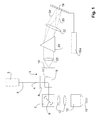
- FIG. 1 shows a schematic view of the basic configuration of a confocal microscope including the essential components, a device according to the present invention being designed as a detector array;
- FIG. 2 shows a schematic view of the basic configuration of an array according to the present invention including SPADs and the option relating thereto for analog or digital circuitry/evaluation;
- FIG. 3 shows a schematic view of the basic configuration of a spectrometer including a device according to the present invention as a detector array;
- FIG. 4 shows schematic views of arrays of a plurality of SiPMs as multipixel SiPMs, for example, for use in a camera ( FIG. 4 a ) or in a spectrometer ( FIG. 4 b );
- FIG. 5 shows schematic views of the use of SPAD arrays as a replacement for conventional photomultipliers
- FIG. 6 shows schematic views of the light distribution ( FIG. 6 a ) and the activation/deactivation of individual SPADs ( FIG. 6 b );
- FIG. 7 shows schematic views of the light distribution ( FIG. 7 a ) and the activation/deactivation of individual SPADs ( FIG. 7 b ), including a smaller light spot in comparison with the representation in FIG. 6 ;
- FIG. 8 shows schematic views of the use of SPAD arrays as a replacement for conventional photomultipliers when working with what are known as SP detectors having a variable aperture;
- FIG. 9 shows schematic views of the use of SPAD arrays as a replacement for conventional photomultipliers when working with what are known as SP detectors having a variable aperture; related-art photomultipliers being replaced by an array of SPADs;
- FIG. 10 shows schematic views of the light distribution ( FIG. 10 a ) and the activation/deactivation of individual SPADs ( FIG. 10 b );
- FIG. 11 shows schematic views of the light distribution ( FIG. 11 a ) and the activation/deactivation of individual SPADs ( FIG. 11 b ) in comparison to the representation in FIG. 10 for a different detection wavelength;
- FIG. 12 shows a schematic view of the basic configuration of an array of SiPMs, FIG. 12 a illustrating the light distribution, and FIG. 12 b the activation/deactivation of individual SPADs;
- FIG. 13 shows a schematic view of the basic configuration of an array of SiPMs, FIG. 13 a illustrating the light distribution, and FIG. 13 b the activation/deactivation of individual SPADs, however, for a different wavelength;
- FIG. 14 shows a schematic view of the light distribution ( FIG. 14 a ) and the activation/deactivation of individual SPADs ( FIG. 14 b ), the SiPMs being linearly arrayed;
- FIG. 15 shows a schematic view of the matrix-type array of a plurality of SiPMs having integrated SPADs, SPADs therein having high dark noise levels being deactivated;
- FIG. 16 shows a schematic view of matrix-like arrayed SiPMs, microlenses being provided there to facilitate light distribution.
- the present invention generally relates to the detection of light, for example, for use in a microscope, a spectrometer, or a camera.
- the device is not limited to a particular application. In the broadest sense, it is to be understood as a detector for light.
- the present invention provides a device for detecting light and a corresponding method, whereby a high image quality, respectively a high signal-to-noise ratio may be achieved at a given illumination/light intensity. It is intended that the device be small in size and inexpensive to manufacture. It is also intended to provide microscopes, spectrometers and cameras that are equipped accordingly.
- the device for detecting light in particular in a microscope, a spectrometer, or a camera, is equipped with at least one silicon photomultiplier (SiPM).
- the silicon photomultiplier is composed of an array of a plurality of single-photon avalanche diodes (SPADs).
- SPADs single-photon avalanche diodes
- the array be larger in area than the incident light, only those SPADs being activated and/or analyzed upon which a specific—high—minimum intensity of light also actually impinges or strikes.
- the device includes a specially adapted SiPM, the SiPM design featuring a high photon detection efficiency (PDE), namely, as in the case of single-photon avalanche diodes (SPADs).
- PDE photon detection efficiency
- SPADs single-photon avalanche diodes
- the response of one single pixel is derived from the number of SPADs combined per pixel, as well as from the dead time of one single SPAD.
- the dead time may be kept very short by “active quenching,” namely within the range of >100 SPAD per pixel and ⁇ 50 ns dead time.
- the SiPMs used here allow selective activation, respectively deactivation of individual SPADs of one pixel.
- An SiPM having digital evaluation electronics is suited for this, in particular.
- an addressable static memory may be used for—selectively—activating individual SPADs directly on a chip.
- SiPMs be able to be manufactured using a conventional CMOS process. Accordingly, such silicon photomultipliers are extremely rugged, particularly under conditions of optical power levels that are high or too high.
- the device advantageously includes a plurality of silicon photomultipliers, each composed of an array of a plurality of single-photon avalanche diodes (SPADs).
- the plurality of SiPMs may be arranged in a matrix, for example, for use in a camera, or linearly side-by-side, for example, for use in a spectrometer.
- the array of the SiPMs is altogether larger in area than the incident light, only those SPADs of the various SiPMs being activated and/or analyzed within the array which are impinged upon, respectively illuminated by a specific—high—minimum intensity of light.
- the device prefferably includes a single silicon photomultiplier having an array of SPADs or an array of a plurality of SiPMs, each having an array of SPADs.
- the minimum intensity of light may be ascertained from one or a plurality of test measurements, respectively from a calibration, at a defined system setting in each case.
- An advantageous aspect of embodiments of the present invention involve minimizing the dark noise of the device, respectively of a correspondingly designed detector, in that only those SPADs are activated which contribute to a high signal-to-noise ratio. Therefore, only those SPADs, respectively pixels are activated upon which detection light is also actually expected. Accordingly, it is also only these—activated—SPADs which contribute to the dark noise.
- the dark noise is caused to a significant degree by defects in the light-sensitive layer of the SPADs.
- the situation may arise where a defective SPAD emits an electronic signal even though no light is incident on the light-sensitive region of the diode.
- the probability of such a false event is referred to as dark count rate, and it should be kept as low as possible.
- the teaching according to the present invention also relates to a device for detecting light, in particular, for use in a microscope, a spectrometer, or a camera, having at least one silicon photomultiplier (SiPM) that is composed of an array of a plurality of single-photon avalanche diodes (SPADs); per SiPM, those SPADs being deactivated or not analyzed, whose operation is less than satisfactory or faulty and, which, therefore, do not “perform” perfectly.
- SiPM silicon photomultiplier
- SPADs single-photon avalanche diodes
- the signal-to-noise ratio of the entire array is substantially improved by deactivating individual SPADs having high dark noise levels, even disregarding the respective detection signal of the SPAD, which is faulty and has, therefore, been deactivated in accordance with the present invention.
- the less than satisfactory or faulty operation of individual SPADs may be defined by a lower threshold value of the ratio of useful signal to dark noise; it not being a matter of a fixed threshold value in this case.
- Test/calibration measurements may be used to ascertain the SPADs which are insufficiently illuminated or whose operation is less than satisfactory or faulty, so that a deactivation of the faulty SPADs over the entire lifetime of the SiPM is possible.
- the SPADs to be deactivated are deactivated via a control, preferably by software, obviating the need for any mechanical intervention into the array.
- the light-sensitive portion of the entire illuminated area referred to as fill factor, is considerably less than 100%, typically within the range of between 50% and 70%.
- a lower photon detection efficiency results therefrom, due, namely, to the light-insensitive regions.
- microlenses respectively a microlens array adapted to the array of the SPADs may be assigned very advantageously to the SPADs of an SiPM.
- the microlenses focus the light, which is incident to the total array, at the respective light-sensitive regions of the SPADs; the fill factor being able to be increased by this measure.
- the SPADs may be arranged on a chip, preferably of a silicon substrate.
- the SiPM chip may be cooled, for example, using thermoselective cooling. A cooling to below ⁇ 40° C. is possible and advantageous.
- a use of the device according to embodiments of the present invention in confocal microscopes is especially beneficial; it being a matter therein of the spectrally selective detection, for example, of fluorescent light coming from a sample. It is useful in this case for the device according to the present invention to be designed along the lines of a detector array.
- the device according to the present invention may also be used in a spectrometer; in the context of such a use, it being known which diode belongs to the respective desired spectral region. Accordingly, only those pixels may be activated upon which detection light is also actually expected in the particular spectral region.
- the use of the device according to the present invention in a camera is also possible, due namely to the previously mentioned properties of an array of SiPMs, composed in each case of arrays of individual SPADs.
- FIG. 1 illustrates the use of a device according to the present invention for detecting light returning from the sample.
- FIG. 1 shows the schematic configuration of a confocal scanning microscope 1 , where an array 19 of SPADs 26 is used for detecting the signals from scanning microscope 1 .
- Illuminating light beam 3 coming from a light source 2 is directed by a beamsplitter or a suitable path-folding means 5 to a scanning device 7 .
- illumination light beam 3 Before striking path-folding means 5 , illumination light beam 3 passes through an illumination pinhole 6 .
- scanning device 7 includes a gimbal-mounted scanning mirror 9 , which directs illuminating light beam 3 through a scanning optical system 12 and a microscope optical system 13 over or through an object 15 .
- illuminating light beam 3 is guided over the object surface.
- illuminating light beam 3 may be directed through the object. If indicated, non-luminous preparations are prepared for these purposes using a suitable dye.
- the dyes optionally present in object 15 are excited by illuminating light beam 3 and emit light in their own characteristic region of the spectrum.
- the light emanating from object 15 defines a detection light beam 17 . It passes through microscope optical system 15 , scanning optical system 12 , and via scanning module 7 to path-folding means 5 , passing therethrough and, via a detection pinhole 18 , to reach array 19 .
- Detection light beam 17 emanating from or defined by object 15 is shown as a dashed line in FIG. 1 .
- Dispersive element 20 spectrally splits detection light beam 17 , thereby spatially and spectrally separating the individual wavelengths of the detection light.
- a lens 21 which expands and parallelizes detection light beam 17 , may be disposed upstream of dispersive element 20 .
- a detector optical system 22 which focuses spectrally separated beams 24 , 25 of detection light beam 17 onto array 19 , may be disposed downstream of dispersive element 20 .
- Spectrally separated beams 24 , 25 differ by wavelength and, therefore, strike different regions on array 19 .
- an expanding optical system 23 is provided upstream of dispersive element 20 . Expanding optical system 23 may be designed in such a way that the numerical aperture of detector optical system 22 is independent of the numerical aperture of detection light beam 17 incident on detection pinhole 18 .
- FIG. 2 shows the basic configuration of an array 19 of a device according to the present invention, array 19 including a plurality of SPADs 26 . Together, SPADs 26 form SiPM 19 ; in this exemplary embodiment, for one pixel.
- FIG. 2 shows the basic circuitry of SiPM 19 , respectively of SPAD 26 in the case of analog evaluation 27 and digital evaluation 28 ; during analog evaluation 27 , the signal being fed to an AD converter 29 and to a corresponding evaluation. During digital evaluation 28 , the signals are fed to a digital evaluation logic 30 (on-chip read out).
- SPADs 26 are individually addressable.
- FIG. 3 shows a basic spectrometer configuration, the light to be detected being parallelized downstream of an aperture/pinhole 32 by an optical system 33 and spectrally split by a dispersive element, for example, a prism, grating 34 or a hologram. Via a further optical system 35 , the spectrally split light reaches a detector array 31 that is designed as a multipixel array having a plurality of SiPMs, composed of SPADs.
- a dispersive element for example, a prism, grating 34 or a hologram.
- the spectrally split light reaches a detector array 31 that is designed as a multipixel array having a plurality of SiPMs, composed of SPADs.
- FIG. 4 shows possible arrangements of SiPMs 19 , each composed of arrays of SPADs 26 .
- SiPMs 19 may, for example, be configured in a matrix-type array for use in a camera ( FIG. 4 a ).
- SiPMs 19 may be linearly arrayed ( FIG. 4 b ) for use in a spectrometer. In each of the two cases, 16 pixels are illustrated, respectively depicted. Other pixel numbers and pixel arrays are possible in light of the present invention.
- FIG. 5 a illustrates the use of conventional photomultipliers 36 , for example, in confocal microscopy, detection light 37 there reaching particular intended photomultipliers 36 via various dichroic beamsplitters 38 to allow detection of specific spectral regions.
- FIG. 5 b shows the replacement of the conventional photomultipliers by arrays of SPADs 26 , it being possible for microlenses to be assigned to SPADs 26 .
- the detection light reaches detectors, in these cases, the arrays of SPADs 26 , namely the various SiPMs 19 which include the SPAD arrays.
- FIG. 6 shows the array of SPADs 26 , which, together, form an SiPM 19 .
- the light distribution is indicated in FIG. 6 a .
- SPADs 26 may feature a distance (subpixel distance) of 50 ⁇ m ⁇ 50 ⁇ m, the pixel size being somewhat smaller, due, namely, to the interpixel distance.
- the photosensitive area may include 40 ⁇ 40 subpixels, for example, this corresponding to the size of a photosensitive area in the range of 2 mm ⁇ 2 mm.
- FIG. 6 b indicates which SPADs 26 are activated, respectively deactivated in accordance with the inventive teaching. SPADs 26 located within the indicated circle and SPADs 26 intersected by the circumference of the circle are activated. SPADs 26 located outside of the circle, respectively not in contact with those within the circle are deactivated, as is claimed by the inventive teaching.
- FIG. 7 shows the same array as in FIG. 6 , however, with a smaller light spot, resulting from a smaller pinhole size.
- FIG. 7 a shows the basic light distribution
- FIG. 7 b the ratio of activated to deactivated SPADs 26 .
- FIG. 8 shows, on the one hand, the basic array in the case of what is known as an SP detector having a variable aperture; FIG. 8 a indicating the conventional use of photomultipliers 36 , while FIG. 8 b shows the use of arrays of SPADs 26 , namely SiPMs 19 , these being able to be equipped, in turn, with or without microlenses.
- Detection light 37 passes an optical system 33 and a prism 39 , is split accordingly—by variable slit or pinhole apertures 40 —and beamsplitters to reach photomultipliers 36 .
- the photomultipliers are replaced by arrays of SPADs 26 , namely by arrays of SiPMs 19 .
- FIG. 9 a illustrates the related art in so far as photomultipliers 36 therein are used along with variable slit or pinhole apertures 40 .
- they are replaced by an array 19 of SPADs 26 .
- Detection light 37 passes accordingly through an optical system 33 and a prism 39 to reach the array (SiPM) composed of individual SPADs 26 .
- the array of SPADs corresponding to the representation in FIG. 8 b is shown in detail in FIG. 10 ; SPADs 26 therein collectively forming a single-pixel SiPM 19 .
- FIG. 10 a again shows the light distribution.
- FIG. 10 b schematically illustrates the activation and deactivation of individual SPADs 26 by the indicated circle.
- FIG. 10 shows an array of SPADs for detecting a first detection wavelength in the context of a use in accordance with FIG. 8 .
- FIG. 11 shows a corresponding array of SPADs 26 , namely, on the one hand, the light distribution, in turn, and, on the other hand, the activation and deactivation of individual SPADs 26 , here, however, with regard to a second detection wavelength in the context an application using an SP detector in accordance with the representation in FIG. 8 .
- FIG. 12 shows the basic configuration of an array of SiPMs 19 , each SiPM including, in turn, a plurality of SPADs 26 .
- FIG. 12 a illustrates the light distribution for a corresponding spot in the context of a spectrometer as shown in FIG. 9 b .
- FIG. 12 b shows the deactivation and activation of an SPAD in accordance with the light distribution.
- FIG. 13 shows the basic configuration of an array of SiPMs 19 in accordance with FIG. 12 , however, having a different light distribution, resulting from a different wavelength, for example, that of fluorescent light.
- FIG. 14 is comparable to that in FIGS. 12 and 13 , the light distribution of the fluorescent light again being different.
- illuminating light 41 of interest for the evaluation and stray light impinge on the array of SiPMs 19 .
- Individual SPADs 26 are deactivated, on the one hand, due to the stray light and, on the other hand, due to the lack of illumination. Activated SPADs 26 are used for the evaluation.
- stray light When used in a spectrometer, specifically that wavelength range in the spectrometer is deactivated in which unwanted stray light, such as reflected or stray light of the excitation laser wavelengths, strikes. If indicated, adjacent ranges are also deactivated due, namely, to what is known as crosstalk. The deactivation of these ranges is particularly important since the stray light is generally much higher in intensity than the useful light (fluorescent light). Since the light distribution of the useful light is dependent on the fluorophores used by the user, all SPADs, respectively pixels are activated upon which no excitation light impinges (provided that they are not defective or dark noise pixels as previously described), so that detection is possible independently of the fluorophores used. Any interference by excitation light is ruled out. In the same way, excitation may be carried out using a plurality of laser lines; a plurality of ranges then being blocked accordingly.
- FIG. 15 shows the configuration of a plurality of SiPMs in the sense of a matrix-type array 19 , each SiPM 19 being composed of a plurality of SPADs 26 . Defective, respectively less than satisfactorily performing SPADs 26 , which cause high dark noise levels, are deactivated.
- FIG. 16 shows the configuration of a plurality of SiPMs 19 , composed in each case of a plurality of SPADs 26 on one chip. Due to the unusable intermediate regions 43 , microlenses 44 , shown in a lateral view in FIG. 16 , are assigned to the arrays of SiPMs 19 . Using microlenses 44 , a more favorable light distribution is derived, in each instance, focused at the usable regions of SiPMs 19 .
- FIG. 16 shows the deactivated SPADs, upon which no detection light impinges.
Landscapes
- Physics & Mathematics (AREA)
- Spectroscopy & Molecular Physics (AREA)
- General Physics & Mathematics (AREA)
- Chemical & Material Sciences (AREA)
- Computer Vision & Pattern Recognition (AREA)
- General Engineering & Computer Science (AREA)
- Engineering & Computer Science (AREA)
- Analytical Chemistry (AREA)
- Optics & Photonics (AREA)
- Spectrometry And Color Measurement (AREA)
- Light Receiving Elements (AREA)
- Photometry And Measurement Of Optical Pulse Characteristics (AREA)
- Microscoopes, Condenser (AREA)
Applications Claiming Priority (3)
| Application Number | Priority Date | Filing Date | Title |
|---|---|---|---|
| DE102011107645.3 | 2011-07-12 | ||
| DE102011107645A DE102011107645A1 (de) | 2011-07-12 | 2011-07-12 | Vorrichtung und Verfahren zum Detektieren von Licht |
| DE102011107645 | 2011-07-12 |
Publications (2)
| Publication Number | Publication Date |
|---|---|
| US20130015331A1 US20130015331A1 (en) | 2013-01-17 |
| US10101203B2 true US10101203B2 (en) | 2018-10-16 |
Family
ID=46516542
Family Applications (1)
| Application Number | Title | Priority Date | Filing Date |
|---|---|---|---|
| US13/545,999 Active 2034-01-15 US10101203B2 (en) | 2011-07-12 | 2012-07-11 | Device and method for detecting light |
Country Status (5)
| Country | Link |
|---|---|
| US (1) | US10101203B2 (de) |
| EP (1) | EP2546621B1 (de) |
| JP (1) | JP6420941B2 (de) |
| CN (1) | CN102879088B (de) |
| DE (1) | DE102011107645A1 (de) |
Cited By (6)
| Publication number | Priority date | Publication date | Assignee | Title |
|---|---|---|---|---|
| WO2020151838A1 (en) * | 2019-01-25 | 2020-07-30 | Carl Zeiss Microscopy Gmbh | Light microscope with photon-counting detector elements and imaging method |
| US10948344B2 (en) * | 2016-08-26 | 2021-03-16 | Halliburton Energy Services, Inc. | Optical fiber spectroscopy using single photon detectors (SPDs) |
| US20210231780A1 (en) * | 2020-01-27 | 2021-07-29 | The Charles Stark Draper Laboratory, Inc. | Beamsplitter Architecture for Monostatic LiDAR |
| US11174175B2 (en) * | 2016-04-13 | 2021-11-16 | Emerging Compounds Treatment Technologies, Inc. | Sustainable system and method for removing and concentrating per- and polyfluoroalkyl substances (PFAS) from water |
| US11520021B2 (en) | 2019-03-19 | 2022-12-06 | Kabushiki Kaisha Toshiba | Light receiving device and range finding device including a switch circuit which re-arranges the order of signals output from a light receiver |
| US12506983B2 (en) | 2023-06-27 | 2025-12-23 | Carl Zeiss Microscopy Gmbh | Method for correcting measurement values of an optical detection channel |
Families Citing this family (98)
| Publication number | Priority date | Publication date | Assignee | Title |
|---|---|---|---|---|
| US20110095192A1 (en) * | 2009-10-26 | 2011-04-28 | Johnson Kurtis F | Method to increase dynamic range of segmented non-linear devices |
| JP2014139564A (ja) * | 2012-12-20 | 2014-07-31 | Sony Corp | 撮像装置および電子機器 |
| ITTO20130538A1 (it) * | 2013-06-28 | 2014-12-28 | St Microelectronics Srl | Sistema e metodo di misura di frequenza di oscillazione per un sensore mems e corrispondente sensore mems |
| GB201317968D0 (en) * | 2013-10-10 | 2013-11-27 | Univ Glasgow | Endoscopy capsule |
| DE102014207599B4 (de) | 2014-04-23 | 2024-09-26 | Robert Bosch Gmbh | Verfahren und Computerprogramm zum Betreiben eines Fotodetektors |
| JP6408796B2 (ja) * | 2014-06-11 | 2018-10-17 | オリンパス株式会社 | レーザ顕微鏡装置 |
| JP6435154B2 (ja) * | 2014-10-14 | 2018-12-05 | 株式会社ジョブ | 光子計数型検出器 |
| EP3213139B1 (de) * | 2014-10-29 | 2021-11-24 | Molecular Devices, LLC | Vorrichtung und verfahren zur erzeugung von fokussierten bildern mit paralleler bildgebung in einem mikroskopsystem |
| US9854231B2 (en) * | 2014-12-18 | 2017-12-26 | General Electric Company | Silicon photomultipliers with internal calibration circuitry |
| JP6333189B2 (ja) * | 2015-02-09 | 2018-05-30 | 三菱電機株式会社 | レーザ受信装置 |
| LU92665B1 (de) * | 2015-02-24 | 2016-08-25 | Leica Microsystems | Verfahren zur verbesserung des dynamikbereichs einer vorrichtung zum detektieren von licht |
| LU92664B1 (de) * | 2015-02-24 | 2016-08-25 | Leica Microsystems | Vorrichtung und verfahren zum detektieren von licht |
| US9819144B2 (en) | 2015-05-14 | 2017-11-14 | Apple Inc. | High-efficiency vertical emitters with improved heat sinking |
| US10034375B2 (en) | 2015-05-21 | 2018-07-24 | Apple Inc. | Circuit substrate with embedded heat sink |
| CN105072358A (zh) * | 2015-06-04 | 2015-11-18 | 南京瑞派宁信息科技有限公司 | 一种少像素相机成像方法及装置 |
| US9735539B2 (en) | 2015-07-20 | 2017-08-15 | Apple Inc. | VCSEL structure with embedded heat sink |
| US10620300B2 (en) | 2015-08-20 | 2020-04-14 | Apple Inc. | SPAD array with gated histogram construction |
| US10324171B2 (en) | 2015-12-20 | 2019-06-18 | Apple Inc. | Light detection and ranging sensor |
| US9997551B2 (en) | 2015-12-20 | 2018-06-12 | Apple Inc. | Spad array with pixel-level bias control |
| US10818471B2 (en) | 2015-12-22 | 2020-10-27 | Hitachi High-Tech Corporation | Charged particle beam device |
| CN105628197A (zh) * | 2015-12-26 | 2016-06-01 | 武汉京邦科技有限公司 | 一种照度计 |
| US9985071B2 (en) | 2016-04-15 | 2018-05-29 | Qualcomm Incorporated | Active area selection for LIDAR receivers |
| US10502830B2 (en) * | 2016-10-13 | 2019-12-10 | Waymo Llc | Limitation of noise on light detectors using an aperture |
| DE102016224162A1 (de) * | 2016-12-05 | 2018-06-07 | Continental Automotive Gmbh | Head-Up-Display |
| JP6639427B2 (ja) | 2017-01-13 | 2020-02-05 | 株式会社東芝 | 受光装置 |
| JP6929671B2 (ja) | 2017-03-17 | 2021-09-01 | キヤノン株式会社 | 撮像装置及び撮像システム |
| JP6867212B2 (ja) * | 2017-03-31 | 2021-04-28 | 株式会社デンソー | 光検出器及び測距装置 |
| US10830879B2 (en) | 2017-06-29 | 2020-11-10 | Apple Inc. | Time-of-flight depth mapping with parallax compensation |
| EP3428574A1 (de) | 2017-07-11 | 2019-01-16 | Fondazione Bruno Kessler | Vorrichtung zur abstandsmessung und verfahren zur messung des abstands |
| CN107422392B (zh) * | 2017-08-08 | 2019-03-08 | 中国科学院西安光学精密机械研究所 | 一种基于单光子探测的绕角定位与追踪系统及方法 |
| KR101938984B1 (ko) * | 2017-08-09 | 2019-04-10 | 연세대학교 산학협력단 | Spad 거리측정 센서 기반의 2단계 트래킹을 이용한 거리 측정 장치 및 방법 |
| US10955552B2 (en) | 2017-09-27 | 2021-03-23 | Apple Inc. | Waveform design for a LiDAR system with closely-spaced pulses |
| JP7096658B2 (ja) * | 2017-10-12 | 2022-07-06 | キヤノン株式会社 | 固体撮像素子及び撮像装置 |
| FR3073050B1 (fr) * | 2017-11-02 | 2023-06-30 | Centre Nat Rech Scient | Appareil et procede de microscopie a fluorescence a super-resolution et de mesure de temps de vie de fluorescence |
| JP6961465B2 (ja) * | 2017-11-07 | 2021-11-05 | キヤノン株式会社 | 電子線検出素子、電子顕微鏡、および、透過型電子顕微鏡 |
| JP6929760B2 (ja) * | 2017-11-07 | 2021-09-01 | キヤノン株式会社 | 電子線検出素子、電子顕微鏡、透過型電子顕微鏡 |
| KR102403544B1 (ko) | 2017-12-18 | 2022-05-30 | 애플 인크. | 방출기들의 어드레스가능 어레이를 사용하는 비행 시간 감지 |
| KR102838795B1 (ko) | 2018-01-23 | 2025-07-25 | 벡톤 디킨슨 앤드 컴퍼니 | 광 검출을 동적 차폐하기 위한 시스템 및 이를 사용하는 방법 |
| CN108375417B (zh) * | 2018-02-28 | 2024-05-10 | 深圳市纽创信安科技开发有限公司 | 一种单光子检测设备 |
| JP6954228B2 (ja) * | 2018-05-22 | 2021-10-27 | 株式会社デンソー | 光検出器およびその制御方法 |
| JP6969504B2 (ja) * | 2018-06-08 | 2021-11-24 | 株式会社デンソー | 測距装置 |
| CO2018007716A1 (es) | 2018-07-25 | 2020-01-31 | Univ Antonio Narino | Receptor para señales ópticas de baja potencia con funcionamiento en condiciones de alta incidencia de luz de fondo y aplicación en comunicación con luz visible |
| WO2020167338A1 (en) | 2019-02-11 | 2020-08-20 | Apple Inc. | Depth sensing using a sparse array of pulsed beams |
| JP6949067B2 (ja) * | 2019-03-05 | 2021-10-13 | キヤノン株式会社 | 撮像素子及びその制御方法、撮像装置、及び、画像処理装置 |
| JP7095626B2 (ja) * | 2019-03-06 | 2022-07-05 | 株式会社デンソー | 光学的測距装置 |
| US11500094B2 (en) | 2019-06-10 | 2022-11-15 | Apple Inc. | Selection of pulse repetition intervals for sensing time of flight |
| WO2020261278A1 (en) * | 2019-06-25 | 2020-12-30 | 5D Sensing Ltd. | Digital readout enabling 2d and 3d analysis for silicon photo multiplier |
| US10881028B1 (en) | 2019-07-03 | 2020-12-29 | Apple Inc. | Efficient heat removal from electronic modules |
| US11555900B1 (en) | 2019-07-17 | 2023-01-17 | Apple Inc. | LiDAR system with enhanced area coverage |
| US11131781B2 (en) | 2019-09-20 | 2021-09-28 | Waymo Llc | Programmable SiPM arrays |
| US11733359B2 (en) * | 2019-12-03 | 2023-08-22 | Apple Inc. | Configurable array of single-photon detectors |
| CN112909033A (zh) | 2019-12-04 | 2021-06-04 | 半导体元件工业有限责任公司 | 半导体器件 |
| CN112909031A (zh) | 2019-12-04 | 2021-06-04 | 半导体元件工业有限责任公司 | 半导体器件 |
| US11764314B2 (en) | 2019-12-04 | 2023-09-19 | Semiconductor Components Industries, Llc | Scattering structures for single-photon avalanche diodes |
| CN112909032A (zh) | 2019-12-04 | 2021-06-04 | 半导体元件工业有限责任公司 | 半导体器件 |
| CN112909034A (zh) | 2019-12-04 | 2021-06-04 | 半导体元件工业有限责任公司 | 半导体器件 |
| CN113132581A (zh) * | 2019-12-31 | 2021-07-16 | 深圳市灵明光子科技有限公司 | 成像方法、成像装置和电子设备 |
| KR20210087349A (ko) | 2020-01-02 | 2021-07-12 | 삼성전자주식회사 | 라이다 장치 및 그 동작 방법 |
| US11646335B2 (en) | 2020-01-30 | 2023-05-09 | Semiconductor Components Industries, Llc | Semiconductor devices with single-photon avalanche diodes and rectangular microlenses |
| US11969259B2 (en) | 2020-02-21 | 2024-04-30 | Hi Llc | Detector assemblies for a wearable module of an optical measurement system and including spring-loaded light-receiving members |
| US11883181B2 (en) | 2020-02-21 | 2024-01-30 | Hi Llc | Multimodal wearable measurement systems and methods |
| US12144653B2 (en) | 2020-02-21 | 2024-11-19 | Hi Llc | Systems, circuits, and methods for reducing common-mode noise in biopotential recordings |
| WO2021167893A1 (en) | 2020-02-21 | 2021-08-26 | Hi Llc | Integrated detector assemblies for a wearable module of an optical measurement system |
| US12029558B2 (en) | 2020-02-21 | 2024-07-09 | Hi Llc | Time domain-based optical measurement systems and methods configured to measure absolute properties of tissue |
| US11950879B2 (en) | 2020-02-21 | 2024-04-09 | Hi Llc | Estimation of source-detector separation in an optical measurement system |
| WO2021167892A1 (en) | 2020-02-21 | 2021-08-26 | Hi Llc | Wearable devices and wearable assemblies with adjustable positioning for use in an optical measurement system |
| US11857348B2 (en) | 2020-03-20 | 2024-01-02 | Hi Llc | Techniques for determining a timing uncertainty of a component of an optical measurement system |
| WO2021188486A1 (en) | 2020-03-20 | 2021-09-23 | Hi Llc | Phase lock loop circuit based adjustment of a measurement time window in an optical measurement system |
| US12085789B2 (en) | 2020-03-20 | 2024-09-10 | Hi Llc | Bias voltage generation in an optical measurement system |
| US11187575B2 (en) | 2020-03-20 | 2021-11-30 | Hi Llc | High density optical measurement systems with minimal number of light sources |
| US12138068B2 (en) | 2020-03-20 | 2024-11-12 | Hi Llc | Techniques for characterizing a nonlinearity of a time-to-digital converter in an optical measurement system |
| US11864867B2 (en) | 2020-03-20 | 2024-01-09 | Hi Llc | Control circuit for a light source in an optical measurement system by applying voltage with a first polarity to start an emission of a light pulse and applying voltage with a second polarity to stop the emission of the light pulse |
| US11607132B2 (en) | 2020-03-20 | 2023-03-21 | Hi Llc | Temporal resolution control for temporal point spread function generation in an optical measurement system |
| US11877825B2 (en) | 2020-03-20 | 2024-01-23 | Hi Llc | Device enumeration in an optical measurement system |
| US11245404B2 (en) | 2020-03-20 | 2022-02-08 | Hi Llc | Phase lock loop circuit based signal generation in an optical measurement system |
| WO2021188485A1 (en) | 2020-03-20 | 2021-09-23 | Hi Llc | Maintaining consistent photodetector sensitivity in an optical measurement system |
| US11903676B2 (en) * | 2020-03-20 | 2024-02-20 | Hi Llc | Photodetector calibration of an optical measurement system |
| US12059262B2 (en) | 2020-03-20 | 2024-08-13 | Hi Llc | Maintaining consistent photodetector sensitivity in an optical measurement system |
| US11876109B2 (en) | 2020-05-06 | 2024-01-16 | Semiconductor Components Industries, Llc | Semiconductor devices with single-photon avalanche diodes and light spreading lenses |
| US11710945B2 (en) | 2020-05-25 | 2023-07-25 | Apple Inc. | Projection of patterned and flood illumination |
| CN113916376B (zh) * | 2020-07-08 | 2025-07-08 | 高利通科技(深圳)有限公司 | 一种光谱仪控制方法及系统 |
| GB202013569D0 (en) * | 2020-08-28 | 2020-10-14 | Ams Int Ag | Dynamic range extension of spad-based devices |
| GB202013584D0 (en) | 2020-08-28 | 2020-10-14 | Ams Int Ag | Dynamic range extension of spad-based devices |
| US11699715B1 (en) | 2020-09-06 | 2023-07-11 | Apple Inc. | Flip-chip mounting of optoelectronic chips |
| JP7423485B2 (ja) * | 2020-09-18 | 2024-01-29 | 株式会社東芝 | 距離計測装置 |
| JP7374937B2 (ja) | 2021-01-13 | 2023-11-07 | 株式会社アドバンテスト | 試験装置、試験方法およびプログラム |
| JP7386190B2 (ja) | 2021-01-21 | 2023-11-24 | 株式会社アドバンテスト | 試験装置、試験方法およびプログラム |
| US12442926B2 (en) | 2021-02-04 | 2025-10-14 | Apple Inc. | Time-of-flight depth sensing with improved linearity |
| CN113009292B (zh) * | 2021-02-25 | 2021-12-28 | 西安交通大学 | 局部放电微光光谱探测器 |
| JP7355773B2 (ja) | 2021-02-26 | 2023-10-03 | 株式会社アドバンテスト | 試験装置、試験方法およびプログラム |
| US12196860B2 (en) | 2021-03-02 | 2025-01-14 | Apple Inc. | Depth sensor calibration using internal reflections |
| US11681028B2 (en) | 2021-07-18 | 2023-06-20 | Apple Inc. | Close-range measurement of time of flight using parallax shift |
| DE102021126145A1 (de) * | 2021-10-08 | 2023-04-13 | Heidelberg Engineering Gmbh | Anordnung mit einem Detektor |
| JP2023181737A (ja) | 2022-06-13 | 2023-12-25 | 株式会社エビデント | レーザ走査型顕微鏡、画像処理装置、レーザ走査型顕微鏡の動作方法、及び、プログラム |
| US12313812B2 (en) | 2022-09-20 | 2025-05-27 | Apple Inc. | MOE-based illumination projector |
| US12123589B1 (en) | 2023-05-22 | 2024-10-22 | Apple Inc. | Flood projector with microlens array |
| WO2025082966A1 (en) | 2023-10-16 | 2025-04-24 | Trinamix Gmbh | Method for evaluating degradation of a photodetector |
| EP4718138A1 (de) * | 2024-09-25 | 2026-04-01 | Leica Microsystems CMS GmbH | Detektionsanordnung, kaskadierte detektionsanordnung und optisches scanmikroskop |
Citations (9)
| Publication number | Priority date | Publication date | Assignee | Title |
|---|---|---|---|---|
| US6335523B1 (en) * | 1998-11-20 | 2002-01-01 | Riken | Semiconductor dark image position sensitive device |
| US6995841B2 (en) * | 2001-08-28 | 2006-02-07 | Rice University | Pulsed-multiline excitation for color-blind fluorescence detection |
| US20070182949A1 (en) | 2005-12-21 | 2007-08-09 | Cristiano Niclass | Method and arrangement for measuring the distance to an object |
| DE102006013290A1 (de) | 2006-03-23 | 2007-09-27 | Robert Bosch Gmbh | Vorrichtung zur optischen Distanzmessung sowie Verfahren zum Betrieb einer solchen Vorrichtung |
| US20080180661A1 (en) * | 2007-01-29 | 2008-07-31 | Brown Gordon C | Chemical analyzer for industrial process control |
| US20100214654A1 (en) | 2007-05-22 | 2010-08-26 | Leica Microsystems Cms Gmbh | Apparatus for the detection of light in a scanning microscope |
| US8193815B2 (en) * | 2007-06-25 | 2012-06-05 | Koninklijke Philips Electronics N.V. | Photodiode self-test |
| US20120248347A1 (en) * | 2011-04-01 | 2012-10-04 | Stmicroelectronics S.R.I. | Confocal optical detector, detector array, and manufacturing method thereof |
| US8582098B2 (en) * | 2007-10-25 | 2013-11-12 | The Research Foundation Of State University Of New York | Single photon spectrometer |
Family Cites Families (5)
| Publication number | Priority date | Publication date | Assignee | Title |
|---|---|---|---|---|
| DE10332193A1 (de) * | 2003-07-15 | 2005-02-03 | Leica Microsystems Heidelberg Gmbh | Detektionsvorrichtung |
| US7403589B1 (en) * | 2007-03-27 | 2008-07-22 | General Electric Company | Photon counting CT detector using solid-state photomultiplier and scintillator |
| JP5475686B2 (ja) * | 2008-01-15 | 2014-04-16 | コーニンクレッカ フィリップス エヌ ヴェ | ソリッドステート放射線検出器 |
| EP2317362B1 (de) * | 2009-10-28 | 2020-01-15 | Carl Zeiss Microscopy GmbH | Mikroskopisches Verfahren und Mikroskop mit gesteigerter Auflösung |
| DE102010055882A1 (de) * | 2010-12-22 | 2012-06-28 | Carl Zeiss Microlmaging Gmbh | Pinhole für ein konfokales Laser-Scanning Mikroskop |
-
2011
- 2011-07-12 DE DE102011107645A patent/DE102011107645A1/de active Pending
-
2012
- 2012-06-29 EP EP12174314.0A patent/EP2546621B1/de active Active
- 2012-07-11 JP JP2012155433A patent/JP6420941B2/ja active Active
- 2012-07-11 US US13/545,999 patent/US10101203B2/en active Active
- 2012-07-11 CN CN201210240807.3A patent/CN102879088B/zh active Active
Patent Citations (10)
| Publication number | Priority date | Publication date | Assignee | Title |
|---|---|---|---|---|
| US6335523B1 (en) * | 1998-11-20 | 2002-01-01 | Riken | Semiconductor dark image position sensitive device |
| US6995841B2 (en) * | 2001-08-28 | 2006-02-07 | Rice University | Pulsed-multiline excitation for color-blind fluorescence detection |
| US20070182949A1 (en) | 2005-12-21 | 2007-08-09 | Cristiano Niclass | Method and arrangement for measuring the distance to an object |
| DE102006013290A1 (de) | 2006-03-23 | 2007-09-27 | Robert Bosch Gmbh | Vorrichtung zur optischen Distanzmessung sowie Verfahren zum Betrieb einer solchen Vorrichtung |
| US7760335B2 (en) | 2006-03-23 | 2010-07-20 | Robert Bosch Gmbh | Device and method for optically measuring distance with detector having photosensitive surfaces |
| US20080180661A1 (en) * | 2007-01-29 | 2008-07-31 | Brown Gordon C | Chemical analyzer for industrial process control |
| US20100214654A1 (en) | 2007-05-22 | 2010-08-26 | Leica Microsystems Cms Gmbh | Apparatus for the detection of light in a scanning microscope |
| US8193815B2 (en) * | 2007-06-25 | 2012-06-05 | Koninklijke Philips Electronics N.V. | Photodiode self-test |
| US8582098B2 (en) * | 2007-10-25 | 2013-11-12 | The Research Foundation Of State University Of New York | Single photon spectrometer |
| US20120248347A1 (en) * | 2011-04-01 | 2012-10-04 | Stmicroelectronics S.R.I. | Confocal optical detector, detector array, and manufacturing method thereof |
Non-Patent Citations (1)
| Title |
|---|
| Frach T et al: "The digital silicon photomultiplier a principle of operation an intrinsic detector performance", Dec. 2009 IEEE Nuclear Science Symposium and Medical imaging Conference. |
Cited By (8)
| Publication number | Priority date | Publication date | Assignee | Title |
|---|---|---|---|---|
| US11174175B2 (en) * | 2016-04-13 | 2021-11-16 | Emerging Compounds Treatment Technologies, Inc. | Sustainable system and method for removing and concentrating per- and polyfluoroalkyl substances (PFAS) from water |
| US10948344B2 (en) * | 2016-08-26 | 2021-03-16 | Halliburton Energy Services, Inc. | Optical fiber spectroscopy using single photon detectors (SPDs) |
| WO2020151838A1 (en) * | 2019-01-25 | 2020-07-30 | Carl Zeiss Microscopy Gmbh | Light microscope with photon-counting detector elements and imaging method |
| US12055700B2 (en) | 2019-01-25 | 2024-08-06 | Carl Zeiss Microscopy Gmbh | Light microscope with photon-counting detector elements and imaging method |
| US11520021B2 (en) | 2019-03-19 | 2022-12-06 | Kabushiki Kaisha Toshiba | Light receiving device and range finding device including a switch circuit which re-arranges the order of signals output from a light receiver |
| US20210231780A1 (en) * | 2020-01-27 | 2021-07-29 | The Charles Stark Draper Laboratory, Inc. | Beamsplitter Architecture for Monostatic LiDAR |
| US11953625B2 (en) * | 2020-01-27 | 2024-04-09 | The Charles Stark Draper Laboratory, Inc. | Beamsplitter architecture for monostatic LiDAR |
| US12506983B2 (en) | 2023-06-27 | 2025-12-23 | Carl Zeiss Microscopy Gmbh | Method for correcting measurement values of an optical detection channel |
Also Published As
| Publication number | Publication date |
|---|---|
| JP2013020972A (ja) | 2013-01-31 |
| CN102879088A (zh) | 2013-01-16 |
| DE102011107645A1 (de) | 2013-01-17 |
| US20130015331A1 (en) | 2013-01-17 |
| CN102879088B (zh) | 2017-04-12 |
| EP2546621A1 (de) | 2013-01-16 |
| EP2546621B1 (de) | 2021-10-06 |
| JP6420941B2 (ja) | 2018-11-07 |
Similar Documents
| Publication | Publication Date | Title |
|---|---|---|
| US10101203B2 (en) | Device and method for detecting light | |
| US8503076B2 (en) | Apparatus for the detection of light in a scanning microscope | |
| US10488251B2 (en) | Method for improving the dynamic range of a device for detecting light | |
| CN107257935B (zh) | 用于探测光的装置和方法 | |
| JP6440622B2 (ja) | サンプル検査システム検出器 | |
| US12014896B2 (en) | Cost effective probing in high volume manufacture of micro LEDs | |
| JP7501532B2 (ja) | 光学測定装置及び光学測定システム | |
| US11982566B2 (en) | System, device, and method for quantum correlation measurement with single photon avalanche diode arrays | |
| JP2011513740A (ja) | 光子混合検出器を用いた時間分解分光分析方法およびシステム | |
| JP2025102913A (ja) | 高速高分解能の顕微鏡検査方法、および高速高分解能の顕微鏡 | |
| US7259366B2 (en) | Apparatus for the detection of photons of a light beam having a three-dimensional array of detectors | |
| CN116710828B (zh) | 具有多个光子计数探测器元件阵列的方法和光学显微镜 | |
| CN100437196C (zh) | 用于探测光束的光子的设备 | |
| US7576316B2 (en) | Apparatus, microscope with an apparatus, and method for calibration of a photosensor chip | |
| US6987274B1 (en) | Light detection and imaging system and method including an array of sensors | |
| US11977216B2 (en) | Light microscope and method of capturing images with a light microscope | |
| Ülkü | Large-format time-gated SPAD cameras for real-time phasor-based FLIM | |
| KR100998015B1 (ko) | 발광소자의 전류분산을 평가하는 방법 및 이를 이용한 평가시스템 | |
| KR101775615B1 (ko) | 고감도 영상 획득방법 | |
| FLIM | Arin Can ÜLKÜ |
Legal Events
| Date | Code | Title | Description |
|---|---|---|---|
| AS | Assignment |
Owner name: LEICA MICROSYSTEMS CMS GMBH, GERMANY Free format text: ASSIGNMENT OF ASSIGNORS INTEREST;ASSIGNORS:BIRK, HOLGER;SEYFRIED, VOLKER;REEL/FRAME:028992/0446 Effective date: 20120710 |
|
| STCF | Information on status: patent grant |
Free format text: PATENTED CASE |
|
| MAFP | Maintenance fee payment |
Free format text: PAYMENT OF MAINTENANCE FEE, 4TH YEAR, LARGE ENTITY (ORIGINAL EVENT CODE: M1551); ENTITY STATUS OF PATENT OWNER: LARGE ENTITY Year of fee payment: 4 |
|
| RR | Request for reexamination filed |
Effective date: 20250822 |
|
| MAFP | Maintenance fee payment |
Free format text: PAYMENT OF MAINTENANCE FEE, 8TH YEAR, LARGE ENTITY (ORIGINAL EVENT CODE: M1552); ENTITY STATUS OF PATENT OWNER: LARGE ENTITY Year of fee payment: 8 |