EP2544512B1 - Haltestromschaltung mit automatischer Auswahl - Google Patents
Haltestromschaltung mit automatischer Auswahl Download PDFInfo
- Publication number
- EP2544512B1 EP2544512B1 EP12156458.7A EP12156458A EP2544512B1 EP 2544512 B1 EP2544512 B1 EP 2544512B1 EP 12156458 A EP12156458 A EP 12156458A EP 2544512 B1 EP2544512 B1 EP 2544512B1
- Authority
- EP
- European Patent Office
- Prior art keywords
- current
- signal
- gate
- flip
- output end
- Prior art date
- Legal status (The legal status is an assumption and is not a legal conclusion. Google has not performed a legal analysis and makes no representation as to the accuracy of the status listed.)
- Active
Links
Images





Classifications
-
- H—ELECTRICITY
- H05—ELECTRIC TECHNIQUES NOT OTHERWISE PROVIDED FOR
- H05B—ELECTRIC HEATING; ELECTRIC LIGHT SOURCES NOT OTHERWISE PROVIDED FOR; CIRCUIT ARRANGEMENTS FOR ELECTRIC LIGHT SOURCES, IN GENERAL
- H05B39/00—Circuit arrangements or apparatus for operating incandescent light sources
- H05B39/04—Controlling
- H05B39/041—Controlling the light-intensity of the source
- H05B39/044—Controlling the light-intensity of the source continuously
-
- H—ELECTRICITY
- H05—ELECTRIC TECHNIQUES NOT OTHERWISE PROVIDED FOR
- H05B—ELECTRIC HEATING; ELECTRIC LIGHT SOURCES NOT OTHERWISE PROVIDED FOR; CIRCUIT ARRANGEMENTS FOR ELECTRIC LIGHT SOURCES, IN GENERAL
- H05B45/00—Circuit arrangements for operating light-emitting diodes [LED]
- H05B45/30—Driver circuits
- H05B45/31—Phase-control circuits
-
- H—ELECTRICITY
- H05—ELECTRIC TECHNIQUES NOT OTHERWISE PROVIDED FOR
- H05B—ELECTRIC HEATING; ELECTRIC LIGHT SOURCES NOT OTHERWISE PROVIDED FOR; CIRCUIT ARRANGEMENTS FOR ELECTRIC LIGHT SOURCES, IN GENERAL
- H05B45/00—Circuit arrangements for operating light-emitting diodes [LED]
- H05B45/30—Driver circuits
- H05B45/357—Driver circuits specially adapted for retrofit LED light sources
- H05B45/3574—Emulating the electrical or functional characteristics of incandescent lamps
- H05B45/3575—Emulating the electrical or functional characteristics of incandescent lamps by means of dummy loads or bleeder circuits, e.g. for dimmers
-
- H—ELECTRICITY
- H05—ELECTRIC TECHNIQUES NOT OTHERWISE PROVIDED FOR
- H05B—ELECTRIC HEATING; ELECTRIC LIGHT SOURCES NOT OTHERWISE PROVIDED FOR; CIRCUIT ARRANGEMENTS FOR ELECTRIC LIGHT SOURCES, IN GENERAL
- H05B45/00—Circuit arrangements for operating light-emitting diodes [LED]
- H05B45/30—Driver circuits
- H05B45/37—Converter circuits
- H05B45/3725—Switched mode power supply [SMPS]
-
- Y—GENERAL TAGGING OF NEW TECHNOLOGICAL DEVELOPMENTS; GENERAL TAGGING OF CROSS-SECTIONAL TECHNOLOGIES SPANNING OVER SEVERAL SECTIONS OF THE IPC; TECHNICAL SUBJECTS COVERED BY FORMER USPC CROSS-REFERENCE ART COLLECTIONS [XRACs] AND DIGESTS
- Y02—TECHNOLOGIES OR APPLICATIONS FOR MITIGATION OR ADAPTATION AGAINST CLIMATE CHANGE
- Y02B—CLIMATE CHANGE MITIGATION TECHNOLOGIES RELATED TO BUILDINGS, e.g. HOUSING, HOUSE APPLIANCES OR RELATED END-USER APPLICATIONS
- Y02B20/00—Energy efficient lighting technologies, e.g. halogen lamps or gas discharge lamps
-
- Y—GENERAL TAGGING OF NEW TECHNOLOGICAL DEVELOPMENTS; GENERAL TAGGING OF CROSS-SECTIONAL TECHNOLOGIES SPANNING OVER SEVERAL SECTIONS OF THE IPC; TECHNICAL SUBJECTS COVERED BY FORMER USPC CROSS-REFERENCE ART COLLECTIONS [XRACs] AND DIGESTS
- Y02—TECHNOLOGIES OR APPLICATIONS FOR MITIGATION OR ADAPTATION AGAINST CLIMATE CHANGE
- Y02B—CLIMATE CHANGE MITIGATION TECHNOLOGIES RELATED TO BUILDINGS, e.g. HOUSING, HOUSE APPLIANCES OR RELATED END-USER APPLICATIONS
- Y02B20/00—Energy efficient lighting technologies, e.g. halogen lamps or gas discharge lamps
- Y02B20/30—Semiconductor lamps, e.g. solid state lamps [SSL] light emitting diodes [LED] or organic LED [OLED]
-
- Y—GENERAL TAGGING OF NEW TECHNOLOGICAL DEVELOPMENTS; GENERAL TAGGING OF CROSS-SECTIONAL TECHNOLOGIES SPANNING OVER SEVERAL SECTIONS OF THE IPC; TECHNICAL SUBJECTS COVERED BY FORMER USPC CROSS-REFERENCE ART COLLECTIONS [XRACs] AND DIGESTS
- Y02—TECHNOLOGIES OR APPLICATIONS FOR MITIGATION OR ADAPTATION AGAINST CLIMATE CHANGE
- Y02B—CLIMATE CHANGE MITIGATION TECHNOLOGIES RELATED TO BUILDINGS, e.g. HOUSING, HOUSE APPLIANCES OR RELATED END-USER APPLICATIONS
- Y02B20/00—Energy efficient lighting technologies, e.g. halogen lamps or gas discharge lamps
- Y02B20/40—Control techniques providing energy savings, e.g. smart controller or presence detection
Definitions
- the disclosure relates to an auto-selecting holding current circuit, and more particularly to an auto-selecting holding current circuit capable of being coupled to different Triodes for Alternating Current (TRIACs).
- TRIACs Alternating Current
- illuminators power consumption of illuminators is usually too high. When strong illumination is not needed, energy can be saved effectively if the illumination of the illuminator can be lowered.
- Common dimmers include TRIAC dimmers, electronic dimmers, and remote control dimmers (such as infrared or radio frequency remote control dimmers).
- the TRIAC dimmer mainly includes a TRIAC for changing the input power of a light, and one of the TRIAC features is the holding-current value.
- the TRIAC When the TRIAC is triggered, the TRIAC maintains a conducting state. When the current flowing through the TRIAC drops below the holding-current value, the TRIAC is closed (or cut off).
- both the input voltage and the input current of the illuminator are decreased, which causes the TRIAC to be closed earlier than expected since the current flowing through the TRIAC is smaller than the holding-current value, and further causes the TRIAC misfire and illuminator to flicker.
- a conventional method for adding a bleeder circuit (or dummy load) in the TRIAC dimmable LED dirver is adopted, so that the current flowing through the TRIAC is higher than the holding-current value even when the TRIAC current is decreased, therefore maintaining normal functions of the TRIAC.
- a common bleeder circuit transmits an extra current extracted from an input voltage to the TRIAC by connecting a constant resistor to the input voltage in parallel, so that the current flowing through the TRIAC is greater than the holding-current value, therefore maintaining the TRIAC turned-on.
- the above method fails to achieve an effect of dynamically compensating for the exact amount of current that the TRIAC lacks. Therefore, a conventional adaptive bleeder circuit is provided to dynamically satisfy the current needed by the TRIAC.
- the adaptive bleeder circuit is merely applicable to the TRIAC having a specific holding-current value.
- the same adaptive bleeder circuit is not applicable to another TRIAC having a different holding-current value. Therefore, the conventional adaptive bleeder circuit is inconvenient in use.
- WO2011/050453 A1 discloses an holding current circuit which is adapted to selectively draw current from a dimmer.
- the disclosure is an auto-selecting holding current circuit, so as to solve a problem that the conventional adaptive bleeder circuit is not applicable to TRIACs having different holding-current values.
- An auto-selecting holding current circuit is applicable to a converter.
- an input voltage which is input into the primary side of the converter is adjusted by a TRIAC.
- the primary side is connected with the TRIAC having a holding-current value.
- a bleeder circuit is mounted at the primary side, and makes an input current flowing through the TRIAC be greater than or equal to the holding current value according to an input current detector signal and a reference current signal.
- the bleeder circuit will output a current to maintain the TRIAC turned-on.
- the different TRIACs have different holding current value.
- the auto-selecting holding current circuit is used to detect the TRIAC holding-current value and modify the bleeder reference voltage level.
- the auto-selecting holding current circuit comprises a first sensor module, a second sensor module and a reference voltage selecting circuit.
- the first sensor module senses a current drop time of the current detector signal or voltage drop time of the input voltage, so as to detect when the TRIAC is turned off and, therefore, outputs a sense signal.
- the second sensor module receives the current detector signal and outputs a critical current signal used to detect a current value range when the TRIAC is turned off.
- the current range stands for the TRIAC holding-current value.
- the reference voltage selecting circuit outputs the reference current signal to the bleeder circuit according to the sense signal and the critical current signal. Therefore, based on the reference current signal, the bleeder circuit maintains the input current of the converter be greater than or equal to the holding-current value.
- the reference voltage selecting circuit obtains a holding-current-value range of the TRIAC to output the corresponding reference current signal to the bleeder circuit, so that the bleeder circuit dynamically adjusts a pulse modulation signal to make the TRIAC operate normally.
- FIG. 1 is a circuit block diagram in which a bleeder circuit is applied in a converter according to an embodiment of the disclosure.
- a bleeder circuit 28 may be applied to a converter 50.
- the converter 50 may be, but is not limited to, an Isolated Converter. That is to say, the converter 50 may also be a Buck Converter, Boost Converter, Buck-boost Converter, Forward Converter, a Half-bridge Converter, a Full-bridge Converter, a Push-Pull Converter or a Flyback Converter.
- the converter 50 has a primary side 51 and a secondary side 52.
- the primary side 51 has an alternating current (AC) signal source 20, a TRIAC 22, a bridge rectifier 23, a current sensor 24, a low pass filter 26 and the bleeder circuit 28.
- the secondary side 52 has a load 30, and the load 30 may be, but is not limited to, Light-Emitting Diodes (LEDs).
- the primary side 51 is supplied with a voltage V IN_2 which is output by the low pass filter 26 with an input of an input voltage V IN .
- the input voltage V IN is the output of the AC signal source 20 passing through the TRIAC 22 and rectified by the bridge rectifier 23.
- FIG 2 is a circuit block diagram of an auto-selecting holding current circuit according to FIG. 1 .
- an auto-selecting holding current circuit 100 which is connected to the primary side 51 comprises a first sensor module 200, a second sensor module 300 and a reference voltage selecting circuit 400.
- the first sensor module 200 is connected to the current sensor 24.
- the first sensor module 200 senses a current drop time (i.e. a current drop when the TRIAC 22 is cut off, for example, the point P in FIG. 3 ) of a current detector signal V CS output by the current sensor 24 (referring to FIG. 3 , which is a schematic time-sequence oscillogram of a current detector signal of FIG.
- the second sensor module 300 receives the current detector signal V CS and outputs a critical current signal V th , in which the critical current signal V th is used to detect the holding-current value I H of the TRIAC 22..
- the reference voltage selecting circuit 400 outputs a reference current signal V Iref to the bleeder circuit 28 according to the sense signal V cd and the critical current signal V th .
- the reference current signal V Iref corresponds to the holding-current value I H of the TRIAC 22.
- the bleeder circuit 28 maintains the input current I IN of the converter, which flows through the TRIAC 22, to be greater than or equal to the holding-current value I H , so as to make the TRIAC 22 operates normally.
- the first sensor module 200 may also be used to sense a voltage drop time of the input voltage V IN (i.e. a voltage drop when the TRIAC 22 is turned off), and then output the sense signal V cd (referring to FIG. 4 , which is a circuit block diagram in which a bleeder circuit is applied in a converter according to another embodiment of the disclosure). It is taken as examples in the following embodiments that the first sensor module 200 senses the current drop of the current detector signal V CS , but these examples are not intended to limit the scope of the disclosure.
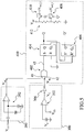
- FIG. 5 is a schematic structural view of a circuit of an auto-selecting holding current circuit according to a first embodiment of the disclosure.
- a first sensor module 200 comprises a differentiator 202 which senses a current drop time for outputting a sense signal V cd to a reference voltage selecting circuit 400.
- FIG. 6A is a schematic structural view of a circuit of a first sensor module according to another embodiment of the disclosure and
- FIG. 6B is a schematic time-sequence oscillogram of a reference voltage and a current detector signal according to FIG. 6A .
- the first sensor module 200 may also comprise a comparator 40.
- the comparator 40 receives a current detector signal V CS and compares the current detector signal V CS to a reference voltage V REF , and thereby, output the sense signal V cd .
- the reference voltage V REF is smaller than a feedback signal value of a holding-current value I H of the TRIAC 22, wherein the feedback signal value of the holding-current value I H is the current detector signal V CS output by a current sensor 24 while a current equal to the holding-current value I H flows through the current sensor 24.
- a second sensor module 300 comprises a comparator 302 and a first NOT gate 304.
- the comparator 302 receives the current detector signal V CS and outputs a comparison signal V C after comparing the current detector signal V CS with a preset current signal V p .
- the first NOT gate 304 receives the comparison signal V C and outputs a critical current signal V th to a reference voltage selecting circuit 400.
- the reference voltage selecting circuit 400 comprises a second AND gate 402, a first reset-set (RS) flip-flop 404, a second RS flip-flop 406, a switch element 408, a switch element 410 and a voltage divider 412.
- An input end 41 of the second AND gate 402 is coupled to the first sensor module 200, and an input end 42 of the second AND gate 402 is coupled to the second sensor module 300.
- An output end 43 of the second AND gate 402 is coupled to a set end S of the first RS flip-flop 404, and an output end Q of the first RS flip-flop 404 is coupled to a reset end R' of the second RS flip-flop 406.
- a reset end R of the first RS flip-flop 404 is grounded, and an output end Q 0 of the first RS flip-flop 404 is coupled to a set end S' of the second RS flip-flop 406.
- An output end Q' of the second RS flip-flop 406 and the output end Q of the first RS flip-flop 406 respectively control the switch elements 408 and 410, so that the voltage divider 412 outputs a reference current signal V Iref .
- the first RS flip-flop 404 and the second RS flip-flop 406 may be, but are not limited to, NAND gate RS flip-flops. However, the embodiment is not intended to limit the disclosure.
- the first RS flip-flop 404 and the second RS flip-flop 406 may be NOR gate RS flip-flops.
- FIG. 7A to FIG. 7D are respectively time-sequence oscillograms of the current detector signal V CS , the sense signal V cd , the critical current signal V th and the reference current signal V Iref in the case of the holding-current value of a TRIAC being greater than a preset current signal value.
- the differentiator 202 When sensing a current drop (namely the point Y in FIG. 7A ), the differentiator 202 outputs the sense signal V cd (namely a pulse signal in FIG. 7B ) to the input end 41 of the second AND gate 402.
- the differentiator 202 is used to detect a sudden drop time of the current detector signal V CS .
- the comparator 302 receives the current detector signal V CS and outputs the comparison signal V C after comparing the current detector signal V CS with the preset current signal V p which corresponds to the preset current signal value.
- the first NOT gate 304 receives the comparison signal V C and outputs the critical current signal V th to the input end 42 of the second AND gate 402. When the current detector signal V CS is greater than the preset current signal V p , the critical current signal V th is at a high level.
- the output end 43 of the second AND gate 402 outputs the high level to the set end S of the first RS flip-flop 404, so that the output end Q of the first RS flip-flop 404 outputs the high level, and the output end Q' of the second RS flip-flop 406 outputs a low level.
- the switch element 410 is actuated, and therefore the voltage divider 412 outputs a corresponding reference current signal V Iref_2 ⁇
- FIG. 8A to FIG. 8D are respectively time-sequence oscillograms of the current detector signal V CS , the sense signal V cd , the critical current signal V th and the reference current signal V I_ref in a case of the holding-current value of a TRIAC being smaller than the preset current signal value.
- the differentiator 202 When sensing a current drop (namely the point Y' in FIG. 8A ), the differentiator 202 outputs the sense signal V cd (namely a pulse signal in FIG. 8B ) to the input end 41 of the second AND gate 402.
- the differentiator 202 is used to detect a sudden drop time of the current detector signal V CS .
- the comparator 302 receives the current detector signal V CS and outputs the comparison signal V C after comparing the current detector signal V CS with the preset current signal V p .
- the first NOT gate 304 receives the comparison signal V C and outputs the critical current signal V th to the input end 42 of the second AND gate 402. When the current detector signal V CS is smaller than the preset current signal V p , the critical current signal V th is at the low level.
- the output end 43 of the second AND gate 402 When the critical current signal V th is at the low level and the differentiator 202 outputs the sense signal V cd , the output end 43 of the second AND gate 402 outputs the low level to the set end S of the first RS flip-flop 404, so that the output end Q of the first RS flip-flop 404 outputs the low level, and the output end Q' of the second RS flip-flop 406 outputs the high level.
- the switch element 408 As the output end Q of the first RS flip-flop 404 outputs the low level, and the output end Q' of the second RS flip-flop 406 outputs the high level, the switch element 408 is actuated, and therefore the voltage divider 412 outputs a corresponding reference current signal V Iref_1 .
- the sudden drop time of the current detector signal V CS is the moment when the input current I IN is smaller than the holding-current value I H which causes the TRIAC turned off. Accordingly, by setting the reference current signal V Iref (namely, V Iref_1 or V Iref_2 ) output by the reference voltage selecting circuit 400 to a value corresponding to the holding-current value I H of the TRIAC 22, the bleeder circuit 28 may control the input current I IN flowing through the TRIAC 22 to be greater than or equal to the holding-current value I H according to the reference current signal V Iref and the current detector signal V CS to make the TRIAC 22 operate normally.
- V Iref namely, V Iref_1 or V Iref_2
- the second sensor module 300 only can provide one single preset current signal, so the auto-selecting holding current circuit 100 is capable of providing two types of reference current signals V Iref .
- the auto-selecting holding current circuit 100 can provide more than two types of reference current signals V Iref , the auto-selecting holding current circuit 100 is capable of providing more than two types of reference current signals V Iref .
- the auto-selecting holding current circuit 100 provides four types of reference current signals V Iref .
- the second embodiment is not intended to limit the disclosure.
- the auto-selecting holding current circuit 100 can provide three types or more than four types of reference current signals V Iref .
- FIG. 9 is a schematic structural view of a circuit of an auto-selecting holding current circuit according to a second embodiment of the disclosure.
- a second sensor module 300 comprises a comparator 330, a comparator 331, a comparator 332, a first NOT gate 333, a first NOT gate 334, a first NOT gate 335, a first AND gate 336 and a first AND gate 337.
- the comparator 330, the comparator 331 and the comparator 332 respectively receive a current detector signal V CS output by a current sensor 24.
- An input end of the first NOT gate 333 is coupled to an output end of the comparator 330.
- An output end of the first NOT gate 333 is coupled to an input end of the first AND gate 336.
- Another input end of the first AND gate 336 is coupled to an output end of the comparator 331.
- An input end of the first NOT gate 334 is coupled to the output end of the comparator 331.
- An output end of the first NOT gate 334 is coupled to an input end of the first AND gate 337.
- Another input end of the first AND gate 337 is coupled to an output end of the comparator 332.
- An input end of the first NOT gate 335 is coupled to the output end of the comparator 332, and an output end of the first NOT gate 335 is coupled to the reference voltage selecting circuit 400.
- the output end of the first NOT gate 335, the output end of the first AND gate 336 and the output end of the first AND gate 337 respectively output a critical current signal V t4 , a critical current signal V t3 and a critical current signal V t2 to the reference voltage selecting circuit 400.
- the reference voltage selecting circuit 400 may comprise a second AND gate 420, a second AND gate 421, a second AND gate 422, an RS flip-flop 423, an RS flip-flop 424, an RS flip-flop 425, an RS flip-flop 426, a first OR gate 427, a first OR gate 428, a switch element 429, a switch element 430, a switch element 431, a switch element 432 and a voltage divider 433.
- An input end of the second AND gate 420 is coupled to an output end of the first AND gate 336; another input end of the second AND gate 420 is coupled to a first sensor module 200; and further another input end of the second AND gate 420 is coupled to an output end Q 03 of the RS flip-flop 425.
- An output end of the second AND gate 420 is coupled to a set end S 2 of the RS flip-flop 424.
- An input end of the second AND gate 421 is coupled to an output end of the first AND gate 337; another input end of the second AND gate 421 is coupled to the first sensor module 200; and further another input end of the second AND gate 421 is coupled to an output end Q 04 of the RS flip-flop 426.
- An output end of the second AND gate 421 is coupled to a set end S 3 of the RS flip-flop 425.
- An input end of the second AND gate 422 is coupled to the output end of the first NOT gate 335; another input end of the second AND gate 422 is coupled to the first sensor module 200.
- An output end of the second AND gate 422 is coupled to a set end S 4 of the RS flip-flop 426.
- An input end of the first OR gate 427 is coupled to an output end Q 2 of the RS flip-flop 424; another input end of the first OR gate 427 is coupled to an output end Q 3 of the RS flip-flop 425; and further another input end of the first OR gate 427 is coupled to an output end Q 4 of the RS flip-flop 426.
- An output end of the first OR gate 427 is coupled to a reset end R 1 of the RS flip-flop 427.
- An input end of the first OR gate 428 is coupled to the output end Q 3 of the RS flip-flop 425; another input end of the first OR gate 428 is coupled to the output end Q 4 of the RS flip-flop 426.
- An output end of the first OR gate 428 is coupled to a reset end R 2 of the RS flip-flop 424.
- an output end Q 02 of the RS flip-flop 424 is coupled to a set end S 1 of the RS flip-flop 423.
- the output end Q 4 of the RS flip-flop 426 is coupled to a reset end R 3 of the RS flip-flop 425.
- the reset end R 4 of the RS flip-flop 426 is grounded.
- An output end Q 1 of the RS flip-flop 423 controls the switch element 429; the output end Q 2 of the RS flip-flop 424 controls the switch element 430; the output end Q 3 of the RS flip-flop 425 controls the switch element 431; and the output end Q 4 of the RS flip-flop 426 controls the switch element 432, so that the voltage divider 433 outputs a corresponding reference current signal V Iref_1 , a reference current signal V Iref_2 , a reference current signal V Iref_3 or a reference current signal V Iref_4 .
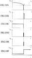
- FIG. 10A to FIG. 10F are respectively time-sequence oscillograms of the current detector signal V CS , the sense signal V cd , the critical current signals V t1 ⁇ V t4 and the reference current signal V Iref in a case of the holding-current value of the TRIAC is greater than a third preset current signal value.
- a current drop namely the point H in FIG. 10A
- the first sensor module 200 outputs a sense signal V cd (namely a pulse signal in FIG. 10B ) to the second AND gate 420, the second AND gate 421 and the second AND gate 422.
- the first sensor module 200 is used to detect a sudden drop time of the current detector signal V CS .
- the comparator 330 receives the current detector signal V CS and outputs a comparison signal V C1 after comparing the current detector signal V CS with a first preset current signal V p1 .
- the first NOT gate 333 receives the comparison signal V C1 and outputs a reversed phase of the comparison signal V C1 to the first AND gate 336.
- the comparator 331 receives the current detector signal V CS and outputs a comparison signal V C2 to the first AND gate 336 and the first NOT gate 334 after comparing the current detector signal V CS with a second preset current signal V p2 .
- the first NOT gate 334 receives the comparison signal V C2 and outputs a reversed phase of the comparison signal V C2 to the first AND gate 337.
- the comparator 332 receives the current detector signal V CS and outputs a comparison signal V C3 to the first AND gate 337 and the first NOT gate 335 after comparing the current detector signal V CS with a third preset current signal V p3 .
- the first NOT gate 335 receives the comparison signal V C3 and outputs a critical current signal V t4 to the second AND gate 422.
- the first AND gate 336 outputs a critical current signal V t2 to the second AND gate 420 according to the reversed phase of the comparison signal V C1 and the comparison signal V C2 .
- the first AND gate 337 outputs a critical current signal V t3 to the second AND gate 421 according to the reversed phase of the comparison signal V C2 and the comparison signal V C3 .
- the third preset current signal V p3 is greater than the second preset current signal V p2
- the second preset current signal V p2 is greater than the first present current signal V p1 .
- the critical current signal V t4 When the current detector signal V CS is greater than the third preset current signal V p3 , the critical current signal V t4 is at a high level.
- the second AND gate 422 When the critical current signal V t4 is at the high level and the first sensor module 200 outputs the sense signal V cd , the second AND gate 422 outputs the high level to the set end S 4 of the RS flip-flop 426, so that the output end Q 4 of the RS flip-flop 426 outputs the high level, the output end Q 3 of the RS flip-flop 425 outputs a low level, the output end Q 2 of the RS flip-flop 424 outputs the low level, and the output end Q 1 of the RS flip-flop 423 outputs the low level.
- the switch element 432 Since the output end Q 4 of the RS flip-flop 426 outputs the high level, the output end Q 3 of the RS flip-flop 425 outputs the low level, the output end Q 2 of the RS flip-flop 424 outputs the low level, and the output end Q 1 of the RS flip-flop 423 outputs the low level, the switch element 432 is actuated, and therefore the voltage divider 433 outputs the corresponding reference current signal V Iref_4 .
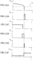
- FIG 11A to FIG.11F are respectively time-sequence oscillograms of the current detector signal V CS , the sense signal V cd , the critical current signals V t1 ⁇ V t4 and the reference current signal V Iref in a case of the holding-current value of the TRIAC being between a second preset current signal and a third preset current signal.
- the current detector signal V CS is greater than the second preset current signal V p2 and smaller than the third preset current signal V p3 , the critical current signal V t4 is at the low level and the critical current signal V t3 is at the high level.
- the second AND gate 422 When the critical current signal V t3 is at the high level and the first sensor module 200 outputs the sense signal V cd , the second AND gate 422 outputs the low level to the set end S 4 of the RS flip-flop 426, so that the output end Q 4 of the RS flip-flop 426 outputs the low level, the output end Q 3 of the RS flip-flop 425 outputs the high level, the output end Q 2 of the RS flip-flop 424 outputs the low level, and the output end Q 1 of the RS flip-flop 423 outputs the low level.
- the switch element 431 Since the output end Q 4 of the RS flip-flop 426 outputs the low level, the output end Q 3 of the RS flip-flop 425 outputs the high level, the output end Q 2 of the RS flip-flop 424 outputs the low level, and the output end Q 1 of the RS flip-flop 423 outputs the low level, the switch element 431 is actuated, and therefore the voltage divider 433 outputs the corresponding reference current signal V Iref_3 .
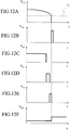
- FIG. 12A to FIG.12F are respectively time-sequence oscillograms of the current detector signal V CS , the sense signal V cd , the critical current signals V t1 ⁇ V t4 and the reference current signal V Iref in a case of the holding-current value of a TRIAC being between a first preset current signal and a second preset current signal.
- the critical current signal V t4 is at the low level
- the critical current signal V t3 is at the low level
- the critical current signal V t2 is at the high level.
- the second AND gate 422 When the critical current signal V t2 is at the high level and the first sensor module 200 outputs the sense signal V cd , the second AND gate 422 outputs the low level to the set end S 4 of the RS flip-flop 426, so that the output end Q 4 of the RS flip-flop 426 outputs the low level, the output end Q 3 of the RS flip-flop 425 outputs the low level, the output end Q 2 of the RS flip-flop 424 outputs the high level, and the output end Q 1 of the RS flip-flop 423 outputs the low level.
- the switch element 430 Since the output end Q 4 of the RS flip-flop 426 outputs the low level, the output end Q 3 of the RS flip-flop 425 outputs the low level, the output end Q 2 of the RS flip-flop 424 outputs the high level, and the output end Q 1 of the RS flip-flop 423 outputs the low level, the switch element 430 is actuated, and therefore the voltage divider 433 outputs the corresponding reference current signal V Iref_2 .
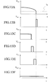
- FIG 13A to FIG 13F are respectively time-sequence oscillograms of the current detector signal V CS , the sense signal V cd , the critical current signals V t1 ⁇ V t4 and the reference current signal V Iref in a case of the holding-current value of the TRIAC being smaller than a first preset current signal.
- the current detector signal V CS is smaller than the first preset current signal V p1
- the critical current signal V t4 is at the low level
- the critical current signal V t3 is at the low level
- the critical current signal V t2 is at the low level.
- the second AND gate 422 When the critical current signal V t2 is at the low level and the first sensor module 200 outputs the sense signal V cd , the second AND gate 422 outputs the low level to the set end S 4 of the RS flip-flop 426, so that the output end Q 4 of the RS flip-flop 426 outputs the low level, the output end Q 3 of the RS flip-flop 425 outputs the low level, the output end Q 2 of the RS flip-flop 424 outputs the low level, and the output end Q 1 of the RS flip-flop 423 outputs the high level.
- the switch element 429 Since the output end Q 4 of the RS flip-flop 426 outputs the low level, the output end Q 3 of the RS flip-flop 425 outputs the low level, the output end Q 2 of the RS flip-flop 424 outputs the low level, and the output end Q 1 of the RS flip-flop 423 outputs the high level, the switch element 429 is actuated, and therefore the voltage divider 433 outputs the corresponding reference current signal V Iref_1 .
- the design of the counter, decoder and preset threshold voltage selecting circuit may be used to achieve the same effect.
- references may be made to the following description of the third embodiment and the fourth embodiment.
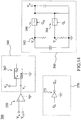
- FIG. 14 is a schematic structural view of a circuit of a auto-selecting holding current circuit according to a third embodiment of the disclosure.
- the first sensor module 200 and the reference voltage selecting circuit 400 are the same as those in the first embodiment, and a second sensor module 300 comprises a comparator 350, a counter 360, a decoder 370 and a preset threshold voltage selecting circuit 380.
- the comparator 350 receives a current detector signal V CS , and outputs a comparison signal V C after comparing the current detector signal V CS with a critical current signal V th (namely a critical current signal V t1 or a critical current signal V t2 , in which the critical current signal V t2 is greater than the critical current signal V t1 ).
- the counter 360 performs cycle count and receives the comparison signal V C to output a count value in real time.
- the decoder 370 continuously receives the count value from the counter 360 and outputs a state signal (in this embodiment, the state signal is an output of an output end Q nb of the second NOT gate 372).
- the preset threshold voltage selecting circuit 380 continuously receives the state signals output by the decoder 370 and outputs the critical current signal V th .
- the counter 360 may also comprise a T flip-flop 362. However, the embodiment is not intended to limit the disclosure; that is to say, the counter 360 may also comprise a D flip-flop.
- a clock end CLK of the T flip-flop 362 is coupled to an output end of the comparator 350.
- An input end T n of the T flip-flop 362 is coupled to a voltage V G which is at a high level.
- the decoder 370 comprises a second NOT gate 372.
- the preset threshold voltage selecting circuit 380 comprises a voltage dividing unit 382, a switch element 384 and a switch element 386.
- An output end of the counter 360 namely an output end Q n of the T flip-flop 362
- an output end Q nb of the second NOT gate 372 respectively control the switch element 384 and the switch element 386, so that the voltage dividing unit 382 outputs the corresponding critical current signal V th .
- the critical current signal is preset to V t2 , and the output end Q n of the T flip-flop 362 is preset to a low level and the output end Q nb of the second NOT gate 372 is preset to a high level, so the switch element 386 is actuated and switch element 384 is opened.
- the comparator 350 receives the current detector signal V CS , and outputs the comparison signal V C after comparing the current detector signal V CS and the critical current signal V t2 .
- the comparison signal V C is at the high level (that is, the current detector signal V CS is smaller than the critical current signal V t2 )
- the output end Q n of the T flip-flop 362 is at the high level
- the output end Q nb of the second NOT gate 372 is at the low level, so that the switch element 384 is actuated, the switch element 386 is opened, and the voltage dividing unit 382 outputs the corresponding critical current signal V t1 .
- the switch element 386 When the comparison signal V C is at the low level (that is, the current detector signal V CS is greater than the critical current signal V t1 ), the output end Q n of the T flip-flop 362 is at the low level (that is, the state signal Q n is at the low level) and the output end Q nb of the second NOT gate 372 is at the high level, so that the switch element 386 is actuated, the switch element 384 is opened, and the voltage dividing unit 382 outputs the corresponding critical current signal V t2 . Therefore, the switch element 384 and the switch element 386 can be actuated in order.
- the second sensor module 300 comprises two types of critical current signals. However, the second sensor module 300 may also comprise more than two types of critical current signals.
- an auto-selecting holding current circuit 100 provides four types of critical current signals. The fourth embodiment is not intended to limit the disclosure. The embodiments of the auto-selecting holding current circuit 100 may also accordingly provide three types or more than four types of reference current signals.
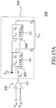
- FIG. 15A and FIG. 15B are respectively schematic structural views of circuits of a comparator, a counter, a decoder and a preset threshold voltage selecting circuit of a auto-selecting holding current circuit according to a fourth embodiment of the disclosure.
- the first sensor module 200 and the reference voltage selecting circuit 400 are the same as those in the second embodiment, and a second sensor module 300 comprises a comparator 350, a counter 360, a decoder 370 and a preset threshold voltage selecting circuit 380.
- the comparator 350 receives a current detector signal V CS , and outputs a comparison signal V C after comparing the current detector signal V CS with a critical current signal V th .
- the counter 360 performs cycle count and receives the comparison signal V C , so as to output a count value C o in real time.
- the decoder 370 continuously receives the count value C o and outputs a state signal (in this embodiment, the state signal is V b1 , V b2 , V b3 or V b4 ).
- the preset threshold voltage selecting circuit 380 continuously receives the state signal and outputs the critical current signal V th (namely, one of the critical current signal V t1 , the critical current signal V t2 , the critical current signal V t3 and the critical current signal V t4 , wherein the critical current signal V t4 is greater than the critical current signal V t3 , the critical current signal V t3 is greater than the critical current signal V t2 , and the critical current signal V t2 is greater than the critical current signal V t1 ).
- the counter 360 comprises a T flip-flop 365 and a T flip-flop 366.
- a clock end CLK 1 of the T flip-flop 365 is coupled to an output end of the comparator 350; an output end Q n1 of the T flip-flop 365 is coupled to a clock end CLK 2 of the T flip-flop 366, and an input end T n1 of the T flip-flop 365 and an input end T n2 of the T flip-flop 366 are coupled to a voltage source V G which is at a high level.
- the decoder 370 comprises a second NOT gate 374, a second NOT gate 375, a third AND gate 376, a third AND gate 377, a third AND gate 378 and a third AND gate 379.
- An input end of the second NOT gate 374 is coupled to an output end Q 1 of the T flip-flop 365, and an output end Q 1b of the second NOT gate 374 is coupled to an input end of the third AND gate 378 and an input end of the third AND gate 379.
- An input end of the second NOT gate 375 is coupled to an output end Q 2 of the T flip-flop 366, and an output end Q 2b of the second NOT gate 375 is coupled to an input end of the third AND gate 377 and an input end of the third AND gate 379.
- the output end Q 1 of the T flip-flop 365 is coupled to an input end of the third AND gate 376 and an input end of the third AND gate 377.
- the output end Q 2 of the T flip-flop 366 is coupled to an input end of the third AND gate 376 and an input end of the third AND gate 378.
- the preset threshold voltage selecting circuit 380 comprises a voltage dividing unit 75, a switch element 76, a switch element 77, a switch element 78 and a switch element 79.
- An output end of the third AND gate 376, an output end of the third AND gate 377, an output end of the third AND gate 378 and an output end of the third AND gate 379 respectively control the voltage dividing unit 75, the switch element 76, the switch element 77, the switch element 78 and the switch element 79, wherein the output end of the third AND gate 376 is used for output the state signal V b4 , the output end of the third AND gate 377 is used for output the state signal V b3 , the output end of the third AND gate 378 is used for output the state signal V b2 and the output end of the third AND gate 379 is used for output the state signal V b1 .
- the critical current signal is preset to V t4
- the output end Q 1 of the T flip-flop 365 is preset to the low level
- the output end Q 2 of the T flip-flop is preset to the low level, so the switch element 79 is actuated.
- the comparator 350 receives the current detector signal V CS , and outputs the comparison signal V C after comparing the current detector signal V CS and the critical current signal V t4 .
- the comparison signal V C is at the high level (that is, the current detector signal V CS is smaller than the critical current signal V t4 )
- the output end Q 1 of the T flip-flop 365 is at the high level
- the output end Q 2 of the T flip-flop 366 is at the low level, so that the switch element 78 is actuated, and the voltage dividing unit 382 outputs the corresponding critical current signal V t3 .
- the comparison signal V C is at the high level (that is, the current detector signal V CS is smaller than the critical current signal V t3 )
- the output end Q 1 of the T flip-flop 365 is at the low level
- the output end Q 2 of the T flip-flop 366 is at the high level, so that the switch element 77 is actuated, and the voltage dividing unit 382 outputs the corresponding critical current signal V t2 .
- the comparison signal V C is at the high level (that is, the current detector signal V CS is smaller than the critical current signal V t2 )
- the output end Q 1 of the T flip-flop 365 is at the high level
- the output end Q 2 of the T flip-flop 366 is at the high level, so that the switch element 76 is actuated, and the voltage dividing unit 382 outputs the corresponding critical current signal V t1 .
- the switch element 76, the switch element 77, the switch element 78 and the switch element 79 can be actuated in order.
- the auto-selecting holding current circuit is applicable to a converter of any type.
- the reference voltage selecting circuit obtains a holding-current value range of the TRIAC to output the corresponding reference current signal to the bleeder circuit, so that the bleeder circuit dynamically adjusts a pulse modulation signal to maintain the normal operation of the TRIAC.
- the second sensor module may output the critical current signal through the design of the counter, decoder and preset threshold voltage selecting circuit.
Landscapes
- Measurement Of Current Or Voltage (AREA)
- Inverter Devices (AREA)
- Circuit Arrangement For Electric Light Sources In General (AREA)
- Electronic Switches (AREA)
- Power Conversion In General (AREA)
Claims (10)
- Auto-Auswahl-Haltstromschaltkreis (100), für einen Wandler (50), wobei eine Eingangsspannung (VIN), die in eine Primärseite (51) des Wandlers (50) eingegeben wird, durch eine Triode für Wechselstrom (22) eingestellt wird, die Primärseite (51) einen Ableitschaltkreis (28) aufweist, die Triode für Wechselstrom (22) weist einen Haltestromwert (IH) auf, der Ableitschaltkreis (28) macht einen Eingangsstrom (IIN), der durch die Triode für Wechselstrom (22) fließt größer als oder gleich zu dem Haltestromwert (IH) entsprechend eines Stromdetektorsignal (Vcs) und einem Referenzstromsignal (IIref), das Stromdetektorsignal (Vcs) entspricht dem Eingangsstrom (IIn); und der Auto-Auswahl-Haltestromkreis (100) umfasst:ein erstes Sensormodul (200), vorzugsweise ein Stromabfalldetektor, dazu ausgebildet eine Stromabfallzeit des Stromabfalldetektorsignals (Vcs) oder eine Spannungsabfallzeit der Eingangsspannung (VIN) zu detektieren, um ein Erkennungssignal (Vcd) auszugeben, wenn die Triode für Wechselstrom ausgeschaltet ist;ein zweites Sensormodul (300), vorzugsweise ein Strombereichsdetektor, dazu ausgebildet das Stromdetektorsignal (Vcs) zu empfangen, um ein kritisches Stromsignal (Vth) auszugeben, wobei das kritische Stromsignal (Vth) ausgebildet ist eine Stromwertebereich des Haltestromwerts (IH) zu beurteilen; unddadurch gekennzeichnet dass der Auto-Auswahl-Haltstromschaltkreis (100) ferner umfasst: einen Referenzspannungsauswahlschaltkreis (400), ausgebildet das Referenzstromsignal (VIref) zu dem Ableitschaltkreis (28) entsprechend des Erkennungssignals (Vcd) und des kritischen Stromsignals (Vth) auszugeben, wobei der Referenzspannungsauswahlschaltkreis (400) ausgebildet ist das Referenzstromsignal (VIref) zu erhöhen, wenn das kritische Stromsignal (Vth) und das Erkennungssignal (Vcd) anzeigen, das der Eingangsstrom (IIN) größer als ein voreingestellter Wert ist und kleiner als der Haltestromwert (IH).
- Auto-Auswahl-Haltstromschaltkreis (100) nach Anspruch 1, wobei das erste Sensormodul (200) einen Differenzierer (202) aufweist, und der Differenzierer (202) die Stromabfallzeit oder die Spannungsabfallzeit detektiert, um das Erkennungssignal (Vcd) auszugeben.
- Auto-Auswahl-Haltstromschaltkreis (100) nach Anspruch 1, wobei das zweite Sensormodul (300) einen Komparator (302) und ein erstes NICHT Gatter (304) umfasst, der Komparator das Stromdetektorsignal (Vcs) empfängt und ein Vergleichssignal (Vc) ausgibt nach vergleichen des Stromdetektorsignal (Vcs) mit einem voreingestellten Stromsignal (Vp) entsprechend dem voreingestellten Wert, und das erste NICHT Gatter (304) empfängt das Vergleichssignal (VC) und gibt das kritische Stromsignal (Vth) aus.
- Auto-Auswahl-Haltstromschaltkreis (100) nach Anspruch 3, wobei der Referenzspannungsauswahlschaltkreis (400) ein zweites UND Gatter (402), ein erstes Reset-Set (RS) Flipflop (404), ein zweites RS Flipflop (406), zwei Schalterelemente (408, 410) und einen Spannungsteiler (412) umfasst; die zwei Eingänge des UND Gatters (402) sind jeweils mit dem ersten Sensormodul (200) und dem zweiten Sensormodul (300) gekoppelt, ein Ausgang (43) des zweiten UND Gatters (402) ist mit einem Set-Eingang (S) des ersten RS Flipflops (404) gekoppelt, ein Ausgang (Q, Q0) des ersten RS Flipflop (404) ist mit einem Reset-Ausgang (R', S') des zweiten RS Flipflops (406) gekoppelt, ein Ausgang (Q') des zweiten RS Flipflop (406) und der Ausgang (Q) des ersten RS Flipflop (404) steuern jeweils ein Schalterelement (408, 410) sodass der Spannungsteiler (412) das entsprechende Referenzstromsignal (VIref, VIref_1, VIref_2) ausgibt.
- Auto-Auswahl-Haltstromschaltkreis (100) nach Anspruch 1, wobei das zweite Sensormodul (300) (N +1) Komparatoren (330, 331, 332), (N+1) erste NICHT Gatter (333, 334, 335) und N erste UND Gatter (336, 337) umfasst, ein Eingang von jeden ersten NICHT Gatter (333, 334, 335) ist jeweils mit einem Ausgang jedes Komparators (330, 331, 332) gekoppelt, ein Ausgang des K'ten ersten NICHT Gatters (333, 334) is jeweils mit einem Eingangs des K'ten ersten UND Gatters (336, 337) gekoppelt, ein anderer Eingang des K'ten ersten UND Gatters (336, 337) ist mit dem Ausgang des (K+1)'ten Komparators (331, 332) gekoppelt, der Ausgang des (K+1)'ten ersten NICHT Gatters (335) und ein Ausgang jedes ersten NICHT Gatters (336, 337) gibt das kritische Stromsignal (Vt2, Vt3, Vt4) aus, wobei N ein positiver Integer ist ,und 1 ≤K≤N.
- Auto-Auswahl-Haltstromschaltkreis (100) nach Anspruch 5, wobei der Referenzspannungsauswahlschaltkreis (400) (N+1) zweite UND Gatter (420, 421, 422), (N+2) RS-Flipflops (423, 424, 425, 426) ein erstes ODER Gatter (427,428), (N+2) Schalterelemente (429, 430, 431, 432) und einen Spannungsteiler (433) umfasst, zwei erste Eingänge des K'ten zweiten UND Gatters (420) sind jeweils mit dem Ausgang des K'ten ersten UND Gatters (336) und des ersten Sensormoduls (200) gekoppelt, zwei Eingänge des (K+1)'ten zweiten UND Gatters (421) sind jeweils mit dem Ausgang des (K+1)'ten ersten UND Gatter (337) gekoppelt und dem ersten Sensormodul (200), ein Augang des K'ten zweiten UND Gatter (420) ist mit einem Set-Eingang (S2) des (K+1)'ten RS Flipflop (424) gekoppelt, ein Ausgang (Q1, Q2, Q3, Q4) von jedem zweiten RS Flipflop (424) zu dem (K+2)'ten RS Flipflop (423, 424, 425, 426, 428) ist mit einem Eingang des ersten ODER Gatters (427, 428) gekoppelt, eine Ausgang des ersten ODER Gatters (427) ist mit einem Reset-Eingang (R1, R2, R3) des ersten RS Flipflops (424, 425, 427) gekoppelt, die Ausgänge (Q2, Q3, Q4) der (N+2) RS Flipflops (424,425, 426) steuern jeweils die (N+2) Schalterelemente (430, 431, 432), sodass der Spannungsteiler (433) das entsprechende Referenzstromsignal (VIref_1, VIref_2, VIref_3, VIref_4) ausgibt.
- Auto-Auswahl-Haltstromschaltkreis (100) nach Anspruch 1, wobei das zweite Sensormodul (300) umfasst:einen Komparator (350), dazu ausgebildet das Stromdetektorsignal (Vcs) zu erhalten und ein Vergleichssignal (Vc) nach vergleichen des Stromdetektorsignals (Vcs) mit dem kritischen Stromsignal (Vth, Vt1, Vt2) auszugeben;einen Zähler (360), dazu ausgebildet eine Zykluszählung durchzuführen und ein Vergleichssignal (Vc) zu erhalten, um einen Zählwert in Echtzeit auszugeben;einen Decoder (370), dazu ausgebildet kontinuierlich den Zählwert zu erhalten, um ein Statussignal auszugeben; undein voreingestellter-Schwellenwert-Spannungsauswahlkreislauf (380), dazu ausgebildet, kontinuierlich den Statussignal zu erhalten, um das kritische Stromwertsignal (Vth) auszugeben.
- Auto-Auswahl-Haltstromschaltkreis (100) nach Anspruch 7, wobei der Zähler (360) einen T-Flipflop (362) umfasst, und ein Uhreingang (CLK) des T Flipflops (362) ist mit einem Ausgang des Komparators (350) gekoppelt.
- Auto-Auswahl-Haltstromschaltkreis (100) nach Anspruch 8, wobei der Decoder (370) ein zweites NICHT Gatter (372) umfasst, ein Eingang des zweiten NICHT Gatters (372) mit dem Zähler (360) gekoppelt ist, und eine Ausgang (Qnb) des zweiten NICHT Gatters (372) mit dem voreingestellter-Schwellenwert-Spannungsauswahlkreislauf (380) gekoppelt ist.
- Auto-Auswahl-Haltstromschaltkreis (100) nach Anspruch 9, wobei der voreingestellter-Schwellenwert-Spannungsauswahlkreislauf (380) eine Spannungsteilereinheit (382) und zwei Schalterelemente (384, 386) umfasst, und ein Ausgang (QN) des Zählers (360) und der Ausgang (Qnb) des zweiten NICHT Gatters (372) jeweils jedes Schalterelement (384, 386) steuern, sodass die Spannungsteilereinheit (382) das entsprechende kritische Stromsignal (Vth) ausgibt.
Applications Claiming Priority (1)
| Application Number | Priority Date | Filing Date | Title |
|---|---|---|---|
| TW100123920A TWI441428B (zh) | 2011-07-06 | 2011-07-06 | 自選維持電流電路 |
Publications (2)
| Publication Number | Publication Date |
|---|---|
| EP2544512A1 EP2544512A1 (de) | 2013-01-09 |
| EP2544512B1 true EP2544512B1 (de) | 2017-02-15 |
Family
ID=45656375
Family Applications (1)
| Application Number | Title | Priority Date | Filing Date |
|---|---|---|---|
| EP12156458.7A Active EP2544512B1 (de) | 2011-07-06 | 2012-02-22 | Haltestromschaltung mit automatischer Auswahl |
Country Status (6)
| Country | Link |
|---|---|
| US (1) | US8575901B2 (de) |
| EP (1) | EP2544512B1 (de) |
| JP (1) | JP5301003B2 (de) |
| KR (1) | KR101351448B1 (de) |
| CN (1) | CN102869146B (de) |
| TW (1) | TWI441428B (de) |
Families Citing this family (29)
| Publication number | Priority date | Publication date | Assignee | Title |
|---|---|---|---|---|
| US8581503B1 (en) * | 2012-05-02 | 2013-11-12 | Semiconductor Components Industries, Llc | Method of forming an LED control circuit and structure therefor |
| US8847498B2 (en) * | 2012-05-16 | 2014-09-30 | Technical Consumer Products, Inc. | Resonant damping circuit for triac dimmable |
| US20130343090A1 (en) * | 2012-06-21 | 2013-12-26 | Fairchild Korea Semiconductor Ltd. | Active bleeder, active bleeding method, and power supply device where the active bleeder is applied |
| CN103024994B (zh) | 2012-11-12 | 2016-06-01 | 昂宝电子(上海)有限公司 | 使用triac调光器的调光控制系统和方法 |
| US9173258B2 (en) * | 2013-03-14 | 2015-10-27 | Cree, Inc. | Lighting apparatus including a current bleeder module for sinking current during dimming of the lighting apparatus and methods of operating the same |
| TW201446072A (zh) * | 2013-05-24 | 2014-12-01 | Lextar Electronics Corp | 應用電路及其控制方法 |
| EP3014952A1 (de) * | 2013-06-27 | 2016-05-04 | Koninklijke Philips N.V. | Auslaufschaltung für einen dämpfer einer leichten nichtlinearen last |
| CN103826362B (zh) * | 2014-01-28 | 2016-03-16 | 杰华特微电子(杭州)有限公司 | 一种led驱动电路及其控制方法 |
| US9912234B2 (en) * | 2014-03-24 | 2018-03-06 | Intersil Americas LLC | Systems and methods for mitigation of resistor nonlinearity errors in single or multiphase switching voltage regulators employing inductor DCR current sensing |
| US9162153B1 (en) * | 2014-04-23 | 2015-10-20 | Innovation First, Inc. | Toy vehicle with an adjustable DC-DC switch |
| US9402293B2 (en) * | 2014-04-24 | 2016-07-26 | Power Integrations, Inc. | Multi-bleeder mode control for improved LED driver performance |
| CN103957634B (zh) | 2014-04-25 | 2017-07-07 | 广州昂宝电子有限公司 | 照明系统及其控制方法 |
| US9484814B2 (en) * | 2014-11-07 | 2016-11-01 | Power Integrations, Inc. | Power converter controller with analog controlled variable current circuit |
| US9692298B2 (en) * | 2014-11-07 | 2017-06-27 | Power Integrations, Inc. | Power converter controller with input current slope adjustment |
| KR102453820B1 (ko) | 2015-08-21 | 2022-10-17 | 서울반도체 주식회사 | 발광소자 구동회로 및 조명장치 |
| US10733944B2 (en) * | 2016-02-19 | 2020-08-04 | Signify Holding B.V. | Configurable modes for lighting systems |
| CN107645804A (zh) | 2017-07-10 | 2018-01-30 | 昂宝电子(上海)有限公司 | 用于led开关控制的系统 |
| CN107682953A (zh) | 2017-09-14 | 2018-02-09 | 昂宝电子(上海)有限公司 | Led照明系统及其控制方法 |
| CN107995730B (zh) | 2017-11-30 | 2020-01-07 | 昂宝电子(上海)有限公司 | 用于与triac调光器有关的基于阶段的控制的系统和方法 |
| CN108200685B (zh) | 2017-12-28 | 2020-01-07 | 昂宝电子(上海)有限公司 | 用于可控硅开关控制的led照明系统 |
| WO2020097754A1 (en) * | 2018-11-12 | 2020-05-22 | Tridonic Gmbh & Co Kg | Power supply circuit, controlling method and lighting driver |
| CN109922564B (zh) | 2019-02-19 | 2023-08-29 | 昂宝电子(上海)有限公司 | 用于triac驱动的电压转换系统和方法 |
| CN110165649B (zh) * | 2019-05-17 | 2024-08-30 | 广州致远电子股份有限公司 | 电源输出泄放电路及电源系统 |
| CN110493913B (zh) | 2019-08-06 | 2022-02-01 | 昂宝电子(上海)有限公司 | 用于可控硅调光的led照明系统的控制系统和方法 |
| CN110831295B (zh) | 2019-11-20 | 2022-02-25 | 昂宝电子(上海)有限公司 | 用于可调光led照明系统的调光控制方法和系统 |
| CN110831289B (zh) | 2019-12-19 | 2022-02-15 | 昂宝电子(上海)有限公司 | Led驱动电路及其操作方法和供电控制模块 |
| CN111031635B (zh) | 2019-12-27 | 2021-11-30 | 昂宝电子(上海)有限公司 | 用于led照明系统的调光系统及方法 |
| CN111432526B (zh) | 2020-04-13 | 2023-02-21 | 昂宝电子(上海)有限公司 | 用于led照明系统的功率因子优化的控制系统和方法 |
| US11539351B1 (en) | 2021-06-17 | 2022-12-27 | Nxp B.V. | Mode detector for DC-DC converters |
Family Cites Families (22)
| Publication number | Priority date | Publication date | Assignee | Title |
|---|---|---|---|---|
| JPS5672366A (en) * | 1979-11-19 | 1981-06-16 | Mitsubishi Electric Corp | Measuring device of holding current of thyristor |
| GB8414451D0 (en) * | 1984-06-06 | 1984-07-11 | Motorola Inc | Crt control circuit |
| JP3120183B2 (ja) * | 1991-05-13 | 2000-12-25 | 株式会社日立製作所 | サイリスタ変換器の制御装置および電力変換器の制御装置 |
| JPH11196529A (ja) * | 1997-12-26 | 1999-07-21 | Toshiba Corp | 電源装置 |
| US7304439B2 (en) * | 2001-09-06 | 2007-12-04 | E. Energy Technology Limited | Phase-controlled dimmable electronic ballasts for fluorescent lamps with very wide dimming range |
| NZ545325A (en) * | 2004-05-19 | 2008-08-29 | Goeken Group Corp | Dynamic snubbing for LED lighting converter |
| JP4569369B2 (ja) * | 2005-04-27 | 2010-10-27 | 住友電気工業株式会社 | 光受信器 |
| JP4972536B2 (ja) * | 2007-12-25 | 2012-07-11 | パナソニック株式会社 | 調光装置 |
| JP4864994B2 (ja) | 2009-03-06 | 2012-02-01 | シャープ株式会社 | Led駆動回路、led照明灯具、led照明機器、及びled照明システム |
| CN101646289A (zh) * | 2009-06-29 | 2010-02-10 | 潘忠浩 | 调光调速控制电路及控制方法 |
| JP5495009B2 (ja) * | 2009-07-14 | 2014-05-21 | ミネベア株式会社 | 照明装置 |
| TW201134305A (en) * | 2009-07-27 | 2011-10-01 | Koninkl Philips Electronics Nv | Bleeder circuit |
| JP4943487B2 (ja) * | 2009-10-26 | 2012-05-30 | シャープ株式会社 | Led駆動回路、led照明灯具、led照明機器、及びled照明システム |
| US8283875B2 (en) * | 2009-10-26 | 2012-10-09 | Light-Based Technologies Incorporated | Holding current circuits for phase-cut power control |
| EP2494852A1 (de) * | 2009-10-30 | 2012-09-05 | Koninklijke Philips Electronics N.V. | Selektiv aktivierte zünd-/ableitschaltung für festkörperbeleuchtungssystem |
| US8294379B2 (en) * | 2009-11-10 | 2012-10-23 | Green Mark Technology Inc. | Dimmable LED lamp and dimmable LED lighting apparatus |
| MX2012005844A (es) | 2009-11-20 | 2012-09-28 | Lutron Electronics Co | Circuito de carga controlable para su uso con un dispositivo de control de carga. |
| US8508147B2 (en) * | 2010-06-01 | 2013-08-13 | United Power Research Technology Corp. | Dimmer circuit applicable for LED device and control method thereof |
| US8111017B2 (en) * | 2010-07-12 | 2012-02-07 | O2Micro, Inc | Circuits and methods for controlling dimming of a light source |
| CN101916547B (zh) * | 2010-07-14 | 2012-10-17 | 成都芯源系统有限公司 | 驱动多个发光元件的驱动器以及显示设备 |
| JP5708371B2 (ja) * | 2010-10-28 | 2015-04-30 | ミツミ電機株式会社 | 照明用電源装置および保持電流の制御方法 |
| US8497637B2 (en) * | 2011-04-13 | 2013-07-30 | Gang Gary Liu | Constant voltage dimmable LED driver |
-
2011
- 2011-07-06 TW TW100123920A patent/TWI441428B/zh active
- 2011-07-12 CN CN201110199234.XA patent/CN102869146B/zh active Active
-
2012
- 2012-02-22 EP EP12156458.7A patent/EP2544512B1/de active Active
- 2012-02-29 KR KR1020120020901A patent/KR101351448B1/ko active Active
- 2012-03-01 US US13/410,034 patent/US8575901B2/en active Active
- 2012-03-19 JP JP2012062039A patent/JP5301003B2/ja active Active
Non-Patent Citations (1)
| Title |
|---|
| None * |
Also Published As
| Publication number | Publication date |
|---|---|
| TW201304368A (zh) | 2013-01-16 |
| KR101351448B1 (ko) | 2014-01-14 |
| US20130009616A1 (en) | 2013-01-10 |
| TWI441428B (zh) | 2014-06-11 |
| JP2013016461A (ja) | 2013-01-24 |
| EP2544512A1 (de) | 2013-01-09 |
| KR20130006271A (ko) | 2013-01-16 |
| CN102869146B (zh) | 2015-01-14 |
| CN102869146A (zh) | 2013-01-09 |
| US8575901B2 (en) | 2013-11-05 |
| JP5301003B2 (ja) | 2013-09-25 |
Similar Documents
| Publication | Publication Date | Title |
|---|---|---|
| US8575901B2 (en) | Auto-selecting holding current circuit | |
| US9161401B1 (en) | LED (light-emitting diode) string derived controller power supply | |
| US9913332B2 (en) | Two-channel LED driver and the control method thereof | |
| US8829819B1 (en) | Enhanced active preload for high performance LED driver with extended dimming | |
| US9119254B2 (en) | Light emitting device power supply circuit with dimming function and control circuit thereof | |
| TWI496507B (zh) | 發光二極體電路及其驅動方法 | |
| US10021754B2 (en) | Two-channel LED driver with short circuit protection and short circuit protection method for two-channel LED driver | |
| CN104168697B (zh) | 用于led驱动电源开关分段调光的输出电流控制电路 | |
| CN103916018A (zh) | 一种开关电源 | |
| CN101868090A (zh) | 用于调光或调速控制的电路及控制方法 | |
| CN103313482A (zh) | 一种led应急照明系统以及led照明灯具 | |
| EP3058794B1 (de) | Ansteuerungsschaltung und verfahren zur steuerung eines beleuchtungselements | |
| CN107210681B (zh) | 用于功率供应装置的功率转换和功率因数校正电路 | |
| CN106714392B (zh) | 带led开路保护的分段开关调光控制驱动电路 | |
| CN103379711A (zh) | Led照明装置 | |
| CN106455205B (zh) | 双通道led驱动器及其开路保护方法 | |
| CN109379806B (zh) | 一种调光驱动电路、调光控制器和led灯具 | |
| CN102244965A (zh) | 照明控制器及照明驱动系统 | |
| CN206533586U (zh) | 带led开路保护的分段开关调光控制驱动电路 | |
| CN203934078U (zh) | Led分段调光电路 | |
| CN206674243U (zh) | 带led开路保护的分段开关调光控制驱动芯片 | |
| CN104159373A (zh) | 基于自适应可变电路的led节能灯及其电路控制方法 | |
| EP2938162B1 (de) | Led-schaltung und ansteuerungsverfahren dafür | |
| CN104640269A (zh) | 光源装置 | |
| US9282602B2 (en) | Light driver control system |
Legal Events
| Date | Code | Title | Description |
|---|---|---|---|
| PUAI | Public reference made under article 153(3) epc to a published international application that has entered the european phase |
Free format text: ORIGINAL CODE: 0009012 |
|
| AK | Designated contracting states |
Kind code of ref document: A1 Designated state(s): AL AT BE BG CH CY CZ DE DK EE ES FI FR GB GR HR HU IE IS IT LI LT LU LV MC MK MT NL NO PL PT RO RS SE SI SK SM TR |
|
| AX | Request for extension of the european patent |
Extension state: BA ME |
|
| 17P | Request for examination filed |
Effective date: 20130314 |
|
| 17Q | First examination report despatched |
Effective date: 20150707 |
|
| GRAP | Despatch of communication of intention to grant a patent |
Free format text: ORIGINAL CODE: EPIDOSNIGR1 |
|
| INTG | Intention to grant announced |
Effective date: 20160907 |
|
| GRAS | Grant fee paid |
Free format text: ORIGINAL CODE: EPIDOSNIGR3 |
|
| GRAA | (expected) grant |
Free format text: ORIGINAL CODE: 0009210 |
|
| AK | Designated contracting states |
Kind code of ref document: B1 Designated state(s): AL AT BE BG CH CY CZ DE DK EE ES FI FR GB GR HR HU IE IS IT LI LT LU LV MC MK MT NL NO PL PT RO RS SE SI SK SM TR |
|
| REG | Reference to a national code |
Ref country code: CH Ref legal event code: EP Ref country code: GB Ref legal event code: FG4D |
|
| REG | Reference to a national code |
Ref country code: IE Ref legal event code: FG4D |
|
| REG | Reference to a national code |
Ref country code: AT Ref legal event code: REF Ref document number: 868545 Country of ref document: AT Kind code of ref document: T Effective date: 20170315 |
|
| REG | Reference to a national code |
Ref country code: DE Ref legal event code: R096 Ref document number: 602012028647 Country of ref document: DE |
|
| REG | Reference to a national code |
Ref country code: NL Ref legal event code: MP Effective date: 20170215 |
|
| REG | Reference to a national code |
Ref country code: LT Ref legal event code: MG4D |
|
| REG | Reference to a national code |
Ref country code: AT Ref legal event code: MK05 Ref document number: 868545 Country of ref document: AT Kind code of ref document: T Effective date: 20170215 |
|
| PG25 | Lapsed in a contracting state [announced via postgrant information from national office to epo] |
Ref country code: HR Free format text: LAPSE BECAUSE OF FAILURE TO SUBMIT A TRANSLATION OF THE DESCRIPTION OR TO PAY THE FEE WITHIN THE PRESCRIBED TIME-LIMIT Effective date: 20170215 Ref country code: GR Free format text: LAPSE BECAUSE OF FAILURE TO SUBMIT A TRANSLATION OF THE DESCRIPTION OR TO PAY THE FEE WITHIN THE PRESCRIBED TIME-LIMIT Effective date: 20170516 Ref country code: LT Free format text: LAPSE BECAUSE OF FAILURE TO SUBMIT A TRANSLATION OF THE DESCRIPTION OR TO PAY THE FEE WITHIN THE PRESCRIBED TIME-LIMIT Effective date: 20170215 Ref country code: NO Free format text: LAPSE BECAUSE OF FAILURE TO SUBMIT A TRANSLATION OF THE DESCRIPTION OR TO PAY THE FEE WITHIN THE PRESCRIBED TIME-LIMIT Effective date: 20170515 Ref country code: FI Free format text: LAPSE BECAUSE OF FAILURE TO SUBMIT A TRANSLATION OF THE DESCRIPTION OR TO PAY THE FEE WITHIN THE PRESCRIBED TIME-LIMIT Effective date: 20170215 |
|
| PG25 | Lapsed in a contracting state [announced via postgrant information from national office to epo] |
Ref country code: NL Free format text: LAPSE BECAUSE OF FAILURE TO SUBMIT A TRANSLATION OF THE DESCRIPTION OR TO PAY THE FEE WITHIN THE PRESCRIBED TIME-LIMIT Effective date: 20170215 Ref country code: LV Free format text: LAPSE BECAUSE OF FAILURE TO SUBMIT A TRANSLATION OF THE DESCRIPTION OR TO PAY THE FEE WITHIN THE PRESCRIBED TIME-LIMIT Effective date: 20170215 Ref country code: RS Free format text: LAPSE BECAUSE OF FAILURE TO SUBMIT A TRANSLATION OF THE DESCRIPTION OR TO PAY THE FEE WITHIN THE PRESCRIBED TIME-LIMIT Effective date: 20170215 Ref country code: ES Free format text: LAPSE BECAUSE OF FAILURE TO SUBMIT A TRANSLATION OF THE DESCRIPTION OR TO PAY THE FEE WITHIN THE PRESCRIBED TIME-LIMIT Effective date: 20170215 Ref country code: SE Free format text: LAPSE BECAUSE OF FAILURE TO SUBMIT A TRANSLATION OF THE DESCRIPTION OR TO PAY THE FEE WITHIN THE PRESCRIBED TIME-LIMIT Effective date: 20170215 Ref country code: BG Free format text: LAPSE BECAUSE OF FAILURE TO SUBMIT A TRANSLATION OF THE DESCRIPTION OR TO PAY THE FEE WITHIN THE PRESCRIBED TIME-LIMIT Effective date: 20170515 Ref country code: PT Free format text: LAPSE BECAUSE OF FAILURE TO SUBMIT A TRANSLATION OF THE DESCRIPTION OR TO PAY THE FEE WITHIN THE PRESCRIBED TIME-LIMIT Effective date: 20170615 Ref country code: AT Free format text: LAPSE BECAUSE OF FAILURE TO SUBMIT A TRANSLATION OF THE DESCRIPTION OR TO PAY THE FEE WITHIN THE PRESCRIBED TIME-LIMIT Effective date: 20170215 |
|
| REG | Reference to a national code |
Ref country code: CH Ref legal event code: PL |
|
| PG25 | Lapsed in a contracting state [announced via postgrant information from national office to epo] |
Ref country code: CZ Free format text: LAPSE BECAUSE OF FAILURE TO SUBMIT A TRANSLATION OF THE DESCRIPTION OR TO PAY THE FEE WITHIN THE PRESCRIBED TIME-LIMIT Effective date: 20170215 Ref country code: LI Free format text: LAPSE BECAUSE OF NON-PAYMENT OF DUE FEES Effective date: 20170228 Ref country code: SK Free format text: LAPSE BECAUSE OF FAILURE TO SUBMIT A TRANSLATION OF THE DESCRIPTION OR TO PAY THE FEE WITHIN THE PRESCRIBED TIME-LIMIT Effective date: 20170215 Ref country code: EE Free format text: LAPSE BECAUSE OF FAILURE TO SUBMIT A TRANSLATION OF THE DESCRIPTION OR TO PAY THE FEE WITHIN THE PRESCRIBED TIME-LIMIT Effective date: 20170215 Ref country code: IT Free format text: LAPSE BECAUSE OF FAILURE TO SUBMIT A TRANSLATION OF THE DESCRIPTION OR TO PAY THE FEE WITHIN THE PRESCRIBED TIME-LIMIT Effective date: 20170215 Ref country code: CH Free format text: LAPSE BECAUSE OF NON-PAYMENT OF DUE FEES Effective date: 20170228 Ref country code: RO Free format text: LAPSE BECAUSE OF FAILURE TO SUBMIT A TRANSLATION OF THE DESCRIPTION OR TO PAY THE FEE WITHIN THE PRESCRIBED TIME-LIMIT Effective date: 20170215 |
|
| REG | Reference to a national code |
Ref country code: DE Ref legal event code: R097 Ref document number: 602012028647 Country of ref document: DE |
|
| REG | Reference to a national code |
Ref country code: IE Ref legal event code: MM4A |
|
| PG25 | Lapsed in a contracting state [announced via postgrant information from national office to epo] |
Ref country code: PL Free format text: LAPSE BECAUSE OF FAILURE TO SUBMIT A TRANSLATION OF THE DESCRIPTION OR TO PAY THE FEE WITHIN THE PRESCRIBED TIME-LIMIT Effective date: 20170215 Ref country code: MC Free format text: LAPSE BECAUSE OF FAILURE TO SUBMIT A TRANSLATION OF THE DESCRIPTION OR TO PAY THE FEE WITHIN THE PRESCRIBED TIME-LIMIT Effective date: 20170215 Ref country code: SM Free format text: LAPSE BECAUSE OF FAILURE TO SUBMIT A TRANSLATION OF THE DESCRIPTION OR TO PAY THE FEE WITHIN THE PRESCRIBED TIME-LIMIT Effective date: 20170215 Ref country code: DK Free format text: LAPSE BECAUSE OF FAILURE TO SUBMIT A TRANSLATION OF THE DESCRIPTION OR TO PAY THE FEE WITHIN THE PRESCRIBED TIME-LIMIT Effective date: 20170215 |
|
| PLBE | No opposition filed within time limit |
Free format text: ORIGINAL CODE: 0009261 |
|
| STAA | Information on the status of an ep patent application or granted ep patent |
Free format text: STATUS: NO OPPOSITION FILED WITHIN TIME LIMIT |
|
| PG25 | Lapsed in a contracting state [announced via postgrant information from national office to epo] |
Ref country code: LU Free format text: LAPSE BECAUSE OF NON-PAYMENT OF DUE FEES Effective date: 20170222 |
|
| 26N | No opposition filed |
Effective date: 20171116 |
|
| GBPC | Gb: european patent ceased through non-payment of renewal fee |
Effective date: 20170515 |
|
| REG | Reference to a national code |
Ref country code: FR Ref legal event code: ST Effective date: 20171227 |
|
| PG25 | Lapsed in a contracting state [announced via postgrant information from national office to epo] |
Ref country code: FR Free format text: LAPSE BECAUSE OF NON-PAYMENT OF DUE FEES Effective date: 20170418 |
|
| REG | Reference to a national code |
Ref country code: BE Ref legal event code: MM Effective date: 20170228 |
|
| PG25 | Lapsed in a contracting state [announced via postgrant information from national office to epo] |
Ref country code: IE Free format text: LAPSE BECAUSE OF NON-PAYMENT OF DUE FEES Effective date: 20170222 Ref country code: SI Free format text: LAPSE BECAUSE OF FAILURE TO SUBMIT A TRANSLATION OF THE DESCRIPTION OR TO PAY THE FEE WITHIN THE PRESCRIBED TIME-LIMIT Effective date: 20170215 |
|
| PG25 | Lapsed in a contracting state [announced via postgrant information from national office to epo] |
Ref country code: GB Free format text: LAPSE BECAUSE OF NON-PAYMENT OF DUE FEES Effective date: 20170515 |
|
| PG25 | Lapsed in a contracting state [announced via postgrant information from national office to epo] |
Ref country code: BE Free format text: LAPSE BECAUSE OF NON-PAYMENT OF DUE FEES Effective date: 20170228 |
|
| PG25 | Lapsed in a contracting state [announced via postgrant information from national office to epo] |
Ref country code: MT Free format text: LAPSE BECAUSE OF NON-PAYMENT OF DUE FEES Effective date: 20170222 |
|
| PG25 | Lapsed in a contracting state [announced via postgrant information from national office to epo] |
Ref country code: HU Free format text: LAPSE BECAUSE OF FAILURE TO SUBMIT A TRANSLATION OF THE DESCRIPTION OR TO PAY THE FEE WITHIN THE PRESCRIBED TIME-LIMIT; INVALID AB INITIO Effective date: 20120222 |
|
| PG25 | Lapsed in a contracting state [announced via postgrant information from national office to epo] |
Ref country code: CY Free format text: LAPSE BECAUSE OF NON-PAYMENT OF DUE FEES Effective date: 20170215 |
|
| PG25 | Lapsed in a contracting state [announced via postgrant information from national office to epo] |
Ref country code: MK Free format text: LAPSE BECAUSE OF FAILURE TO SUBMIT A TRANSLATION OF THE DESCRIPTION OR TO PAY THE FEE WITHIN THE PRESCRIBED TIME-LIMIT Effective date: 20170215 |
|
| PG25 | Lapsed in a contracting state [announced via postgrant information from national office to epo] |
Ref country code: TR Free format text: LAPSE BECAUSE OF FAILURE TO SUBMIT A TRANSLATION OF THE DESCRIPTION OR TO PAY THE FEE WITHIN THE PRESCRIBED TIME-LIMIT Effective date: 20170215 |
|
| PG25 | Lapsed in a contracting state [announced via postgrant information from national office to epo] |
Ref country code: AL Free format text: LAPSE BECAUSE OF FAILURE TO SUBMIT A TRANSLATION OF THE DESCRIPTION OR TO PAY THE FEE WITHIN THE PRESCRIBED TIME-LIMIT Effective date: 20170215 Ref country code: IS Free format text: LAPSE BECAUSE OF FAILURE TO SUBMIT A TRANSLATION OF THE DESCRIPTION OR TO PAY THE FEE WITHIN THE PRESCRIBED TIME-LIMIT Effective date: 20170615 |
|
| P01 | Opt-out of the competence of the unified patent court (upc) registered |
Effective date: 20230601 |
|
| PGFP | Annual fee paid to national office [announced via postgrant information from national office to epo] |
Ref country code: DE Payment date: 20260102 Year of fee payment: 15 |