EP2544234A1 - Verfahren zur Fertigung einer lichtemittierenden Vorrichtung - Google Patents
Verfahren zur Fertigung einer lichtemittierenden Vorrichtung Download PDFInfo
- Publication number
- EP2544234A1 EP2544234A1 EP12186956A EP12186956A EP2544234A1 EP 2544234 A1 EP2544234 A1 EP 2544234A1 EP 12186956 A EP12186956 A EP 12186956A EP 12186956 A EP12186956 A EP 12186956A EP 2544234 A1 EP2544234 A1 EP 2544234A1
- Authority
- EP
- European Patent Office
- Prior art keywords
- solder
- chip mounting
- contact
- layer
- mounting region
- Prior art date
- Legal status (The legal status is an assumption and is not a legal conclusion. Google has not performed a legal analysis and makes no representation as to the accuracy of the status listed.)
- Withdrawn
Links
Images

Classifications
-
- H—ELECTRICITY
- H01—ELECTRIC ELEMENTS
- H01L—SEMICONDUCTOR DEVICES NOT COVERED BY CLASS H10
- H01L33/00—Semiconductor devices with at least one potential-jump barrier or surface barrier specially adapted for light emission; Processes or apparatus specially adapted for the manufacture or treatment thereof or of parts thereof; Details thereof
- H01L33/48—Semiconductor devices with at least one potential-jump barrier or surface barrier specially adapted for light emission; Processes or apparatus specially adapted for the manufacture or treatment thereof or of parts thereof; Details thereof characterised by the semiconductor body packages
- H01L33/483—Containers
-
- H—ELECTRICITY
- H01—ELECTRIC ELEMENTS
- H01L—SEMICONDUCTOR DEVICES NOT COVERED BY CLASS H10
- H01L25/00—Assemblies consisting of a plurality of individual semiconductor or other solid state devices ; Multistep manufacturing processes thereof
- H01L25/16—Assemblies consisting of a plurality of individual semiconductor or other solid state devices ; Multistep manufacturing processes thereof the devices being of types provided for in two or more different main groups of groups H01L27/00 - H01L33/00, or in a single subclass of H10K, H10N, e.g. forming hybrid circuits
- H01L25/167—Assemblies consisting of a plurality of individual semiconductor or other solid state devices ; Multistep manufacturing processes thereof the devices being of types provided for in two or more different main groups of groups H01L27/00 - H01L33/00, or in a single subclass of H10K, H10N, e.g. forming hybrid circuits comprising optoelectronic devices, e.g. LED, photodiodes
-
- H—ELECTRICITY
- H01—ELECTRIC ELEMENTS
- H01L—SEMICONDUCTOR DEVICES NOT COVERED BY CLASS H10
- H01L33/00—Semiconductor devices with at least one potential-jump barrier or surface barrier specially adapted for light emission; Processes or apparatus specially adapted for the manufacture or treatment thereof or of parts thereof; Details thereof
- H01L33/005—Processes
-
- H—ELECTRICITY
- H01—ELECTRIC ELEMENTS
- H01L—SEMICONDUCTOR DEVICES NOT COVERED BY CLASS H10
- H01L33/00—Semiconductor devices with at least one potential-jump barrier or surface barrier specially adapted for light emission; Processes or apparatus specially adapted for the manufacture or treatment thereof or of parts thereof; Details thereof
- H01L33/48—Semiconductor devices with at least one potential-jump barrier or surface barrier specially adapted for light emission; Processes or apparatus specially adapted for the manufacture or treatment thereof or of parts thereof; Details thereof characterised by the semiconductor body packages
- H01L33/64—Heat extraction or cooling elements
-
- H—ELECTRICITY
- H05—ELECTRIC TECHNIQUES NOT OTHERWISE PROVIDED FOR
- H05K—PRINTED CIRCUITS; CASINGS OR CONSTRUCTIONAL DETAILS OF ELECTRIC APPARATUS; MANUFACTURE OF ASSEMBLAGES OF ELECTRICAL COMPONENTS
- H05K1/00—Printed circuits
- H05K1/02—Details
- H05K1/0201—Thermal arrangements, e.g. for cooling, heating or preventing overheating
- H05K1/0203—Cooling of mounted components
- H05K1/021—Components thermally connected to metal substrates or heat-sinks by insert mounting
-
- H—ELECTRICITY
- H05—ELECTRIC TECHNIQUES NOT OTHERWISE PROVIDED FOR
- H05K—PRINTED CIRCUITS; CASINGS OR CONSTRUCTIONAL DETAILS OF ELECTRIC APPARATUS; MANUFACTURE OF ASSEMBLAGES OF ELECTRICAL COMPONENTS
- H05K1/00—Printed circuits
- H05K1/18—Printed circuits structurally associated with non-printed electric components
- H05K1/182—Printed circuits structurally associated with non-printed electric components associated with components mounted in the printed circuit board, e.g. insert mounted components [IMC]
-
- H—ELECTRICITY
- H05—ELECTRIC TECHNIQUES NOT OTHERWISE PROVIDED FOR
- H05K—PRINTED CIRCUITS; CASINGS OR CONSTRUCTIONAL DETAILS OF ELECTRIC APPARATUS; MANUFACTURE OF ASSEMBLAGES OF ELECTRICAL COMPONENTS
- H05K3/00—Apparatus or processes for manufacturing printed circuits
- H05K3/0058—Laminating printed circuit boards onto other substrates, e.g. metallic substrates
- H05K3/0061—Laminating printed circuit boards onto other substrates, e.g. metallic substrates onto a metallic substrate, e.g. a heat sink
-
- H—ELECTRICITY
- H01—ELECTRIC ELEMENTS
- H01L—SEMICONDUCTOR DEVICES NOT COVERED BY CLASS H10
- H01L2224/00—Indexing scheme for arrangements for connecting or disconnecting semiconductor or solid-state bodies and methods related thereto as covered by H01L24/00
- H01L2224/01—Means for bonding being attached to, or being formed on, the surface to be connected, e.g. chip-to-package, die-attach, "first-level" interconnects; Manufacturing methods related thereto
- H01L2224/42—Wire connectors; Manufacturing methods related thereto
- H01L2224/47—Structure, shape, material or disposition of the wire connectors after the connecting process
- H01L2224/48—Structure, shape, material or disposition of the wire connectors after the connecting process of an individual wire connector
- H01L2224/4805—Shape
- H01L2224/4809—Loop shape
- H01L2224/48091—Arched
-
- H—ELECTRICITY
- H01—ELECTRIC ELEMENTS
- H01L—SEMICONDUCTOR DEVICES NOT COVERED BY CLASS H10
- H01L2224/00—Indexing scheme for arrangements for connecting or disconnecting semiconductor or solid-state bodies and methods related thereto as covered by H01L24/00
- H01L2224/01—Means for bonding being attached to, or being formed on, the surface to be connected, e.g. chip-to-package, die-attach, "first-level" interconnects; Manufacturing methods related thereto
- H01L2224/42—Wire connectors; Manufacturing methods related thereto
- H01L2224/47—Structure, shape, material or disposition of the wire connectors after the connecting process
- H01L2224/48—Structure, shape, material or disposition of the wire connectors after the connecting process of an individual wire connector
- H01L2224/481—Disposition
- H01L2224/48151—Connecting between a semiconductor or solid-state body and an item not being a semiconductor or solid-state body, e.g. chip-to-substrate, chip-to-passive
- H01L2224/48221—Connecting between a semiconductor or solid-state body and an item not being a semiconductor or solid-state body, e.g. chip-to-substrate, chip-to-passive the body and the item being stacked
- H01L2224/48225—Connecting between a semiconductor or solid-state body and an item not being a semiconductor or solid-state body, e.g. chip-to-substrate, chip-to-passive the body and the item being stacked the item being non-metallic, e.g. insulating substrate with or without metallisation
- H01L2224/48227—Connecting between a semiconductor or solid-state body and an item not being a semiconductor or solid-state body, e.g. chip-to-substrate, chip-to-passive the body and the item being stacked the item being non-metallic, e.g. insulating substrate with or without metallisation connecting the wire to a bond pad of the item
-
- H—ELECTRICITY
- H01—ELECTRIC ELEMENTS
- H01L—SEMICONDUCTOR DEVICES NOT COVERED BY CLASS H10
- H01L2224/00—Indexing scheme for arrangements for connecting or disconnecting semiconductor or solid-state bodies and methods related thereto as covered by H01L24/00
- H01L2224/73—Means for bonding being of different types provided for in two or more of groups H01L2224/10, H01L2224/18, H01L2224/26, H01L2224/34, H01L2224/42, H01L2224/50, H01L2224/63, H01L2224/71
- H01L2224/732—Location after the connecting process
- H01L2224/73251—Location after the connecting process on different surfaces
- H01L2224/73265—Layer and wire connectors
-
- H—ELECTRICITY
- H01—ELECTRIC ELEMENTS
- H01L—SEMICONDUCTOR DEVICES NOT COVERED BY CLASS H10
- H01L25/00—Assemblies consisting of a plurality of individual semiconductor or other solid state devices ; Multistep manufacturing processes thereof
- H01L25/03—Assemblies consisting of a plurality of individual semiconductor or other solid state devices ; Multistep manufacturing processes thereof all the devices being of a type provided for in the same subgroup of groups H01L27/00 - H01L33/00, or in a single subclass of H10K, H10N, e.g. assemblies of rectifier diodes
- H01L25/04—Assemblies consisting of a plurality of individual semiconductor or other solid state devices ; Multistep manufacturing processes thereof all the devices being of a type provided for in the same subgroup of groups H01L27/00 - H01L33/00, or in a single subclass of H10K, H10N, e.g. assemblies of rectifier diodes the devices not having separate containers
- H01L25/075—Assemblies consisting of a plurality of individual semiconductor or other solid state devices ; Multistep manufacturing processes thereof all the devices being of a type provided for in the same subgroup of groups H01L27/00 - H01L33/00, or in a single subclass of H10K, H10N, e.g. assemblies of rectifier diodes the devices not having separate containers the devices being of a type provided for in group H01L33/00
- H01L25/0753—Assemblies consisting of a plurality of individual semiconductor or other solid state devices ; Multistep manufacturing processes thereof all the devices being of a type provided for in the same subgroup of groups H01L27/00 - H01L33/00, or in a single subclass of H10K, H10N, e.g. assemblies of rectifier diodes the devices not having separate containers the devices being of a type provided for in group H01L33/00 the devices being arranged next to each other
-
- H—ELECTRICITY
- H01—ELECTRIC ELEMENTS
- H01L—SEMICONDUCTOR DEVICES NOT COVERED BY CLASS H10
- H01L2924/00—Indexing scheme for arrangements or methods for connecting or disconnecting semiconductor or solid-state bodies as covered by H01L24/00
- H01L2924/10—Details of semiconductor or other solid state devices to be connected
- H01L2924/1015—Shape
- H01L2924/10155—Shape being other than a cuboid
-
- H—ELECTRICITY
- H05—ELECTRIC TECHNIQUES NOT OTHERWISE PROVIDED FOR
- H05K—PRINTED CIRCUITS; CASINGS OR CONSTRUCTIONAL DETAILS OF ELECTRIC APPARATUS; MANUFACTURE OF ASSEMBLAGES OF ELECTRICAL COMPONENTS
- H05K2201/00—Indexing scheme relating to printed circuits covered by H05K1/00
- H05K2201/10—Details of components or other objects attached to or integrated in a printed circuit board
- H05K2201/10007—Types of components
- H05K2201/10106—Light emitting diode [LED]
-
- H—ELECTRICITY
- H05—ELECTRIC TECHNIQUES NOT OTHERWISE PROVIDED FOR
- H05K—PRINTED CIRCUITS; CASINGS OR CONSTRUCTIONAL DETAILS OF ELECTRIC APPARATUS; MANUFACTURE OF ASSEMBLAGES OF ELECTRICAL COMPONENTS
- H05K2201/00—Indexing scheme relating to printed circuits covered by H05K1/00
- H05K2201/20—Details of printed circuits not provided for in H05K2201/01 - H05K2201/10
- H05K2201/2081—Compound repelling a metal, e.g. solder
-
- H—ELECTRICITY
- H05—ELECTRIC TECHNIQUES NOT OTHERWISE PROVIDED FOR
- H05K—PRINTED CIRCUITS; CASINGS OR CONSTRUCTIONAL DETAILS OF ELECTRIC APPARATUS; MANUFACTURE OF ASSEMBLAGES OF ELECTRICAL COMPONENTS
- H05K2203/00—Indexing scheme relating to apparatus or processes for manufacturing printed circuits covered by H05K3/00
- H05K2203/03—Metal processing
- H05K2203/0315—Oxidising metal
-
- H—ELECTRICITY
- H05—ELECTRIC TECHNIQUES NOT OTHERWISE PROVIDED FOR
- H05K—PRINTED CIRCUITS; CASINGS OR CONSTRUCTIONAL DETAILS OF ELECTRIC APPARATUS; MANUFACTURE OF ASSEMBLAGES OF ELECTRICAL COMPONENTS
- H05K3/00—Apparatus or processes for manufacturing printed circuits
- H05K3/30—Assembling printed circuits with electric components, e.g. with resistor
- H05K3/32—Assembling printed circuits with electric components, e.g. with resistor electrically connecting electric components or wires to printed circuits
- H05K3/34—Assembling printed circuits with electric components, e.g. with resistor electrically connecting electric components or wires to printed circuits by soldering
- H05K3/341—Surface mounted components
Definitions
- the invention relates to a method for the production of lamps and in particular to a method for the production of modules with optoelectronic components.
- optoelectronic components are becoming increasingly important.
- simple bulbs such as lamps also include backlights, for example, for LCD screens or monitors.
- optoelectronic component denotes an element which emits light in an operation when supplied with electrical energy.
- light-emitting diodes based on semiconductors, these include organic light-emitting diodes, combinations of organic and inorganic compounds suitable for light emission, and other light-emitting components.
- the luminance and the uniformity can be improved by suitable structuring of a planar chip mounting region on which the individual luminous bodies are applied.
- a support serving as a heat sink which comprises a flat chip mounting region.
- the carrier may comprise a metal core, a metal substrate with such a planar chip mounting region.
- a ceramic substrate with a metallized chip mounting area, a PCB (Printed Circuit Board) with a planar possibly metallized chip mounting area, or even a leadframe with such a area can be provided as the carrier.
- the subsequent chip mounting area is pretreated, for example metallized.
- any SMT-capable substrate is suitable that can be metallized in partial areas to form a flat chip mounting area.
- the planar chip mounting region is structured to produce a first subregion and at least one second subregion.
- the structuring takes place in such a way that the first subregion has a solder-repelling property after structuring.
- the first subregion is solder-repellent, so that the chip mounting region is solder-repellent in the first sub-region and perpendicular-attracting in the second subregion.
- solder-repellent or "solder-repellent property” is understood to mean a property of the first sub-area, which means that in the event of later application of a solder or solder, these do not or hardly wet the first sub-area. Consequently, after the application of a solder on the flat chip mounting region, the solder mainly concentrates in the second partial region and wets it.
- At least one optoelectronic body preferably an optoelectronic semiconductor component
- the optoelectronic body applied to the solder is thus fixed in the second subarea.
- the optoelectronic body floating on the solder "follows" the solder into the second partial region, since only in this partial region the solder wets the chip mounting region.
- the structuring of the areal chip mounting area into subareas with solder-repelling and volume-attracting or wetting property thus makes it possible to form subregions in which one or more optoelectronic bodies are fixed and connected to the chip mounting area by a previously applied solder.
- an electrical contact suitable for supplying electrical energy to the optoelectronic luminous body, are formed.
- the support serving as a heat sink as an electrode or the planar chip mounting region as an electrode.
- the area chip mounting area serves not only as part of the heat sink, but also as an electrical contact to the optoelectronic device.
- the planar chip mounting region in the second subregion comprises at least one metallic sublayer which is at least partially wettable by the solder.
- the sub-layer may comprise, for example, gold, silver or another non-oxidizing material.
- the planar mounting area comprises different superimposed partial layers of different metals. These metals may include, for example, nickel, copper, aluminum, silver, gold, titanium or tungsten. In this case, a gold layer may be applied over a nickel layer in order to prevent diffusion of gold into underlying sublayers, for example of copper.
- the method it is proposed to remove parts of the gold layer within the chip mounting region and to oxidise the underlying nickel layer in order to structure the chip mounting region and to produce the first partial region.
- the underlying layer in particular a nickel layer, a first portion is created, which has a solder-repellent property, so that the solder applied thereto does not or only very slightly wets this portion.
- such structuring is achieved by providing an optical light source, preferably a laser. Subsequently, in order to produce the structuring of the planar chip mounting region, the first subarea of the planar chip mounting region is irradiated with the optical light source and thus at least one of the metallic sublayers is oxidized.
- irradiation melts or vaporizes a surface material of the first portion and oxidizes an underlying exposed material.
- This underlying oxidized material has the solder repellent properties.
- the surface material may be gold, aluminum or silver, which is evaporated by the irradiation, preferably by means of a laser.
- An underlying material forming another sublayer is exposed. This may include, for example, nickel. The exposed material is then oxidized, for example by means of the optical radiation source, but also by other physical or chemical processes.
- a surface material of the areal chip mounting area may be chemically altered and bonded by physical or chemical methods.
- the areal chip mounting area is structured by applying a solder stop layer on the flat chip mounting area.
- This solder resist is also solder repellent.
- the solder stop layer is patterned to produce the first and second subregions and then removed in the second subarea, so that the underlying surface of the second subarea of the chip mounting region is exposed again.
- a structuring of the solder stop layer can be carried out, for example, by suitable masking methods and exposure. The remaining solder stop layer remains on the chip mounting area to form the first portion.
- a solder stop layer is applied selectively directly to the planar chip mounting region, thus defining the first subregion.
- the solder resist is solder resistant.
- Such an application can take place, for example, by means of a stencil method or a solder dispensing method. If necessary, by exposing and / or processing sections of the second subarea, these can then be cleaned by an undesired solder resist layer, so that the second subarea again comprises the surface wettable by solder.
- the chip mounting area is set deeper within the carrier than the surrounding area, which may contain, for example, the supply line or other electrical contacts.
- a serving as a heat sink carrier is provided with a flat chip mounting area and applied to this a contacting layer.
- the carrier may be a PCB, a ceramic substrate, a metal core, a plastic or even a combination of these carrier materials.
- a dielectric layer is applied flat to the substrate to avoid shorting the chip mounting area.
- Conductor tracks and contact pads as well as other necessary elements are now vapor-deposited, deposited or otherwise applied to the dielectric layer.
- the chip mounting area is further structured accordingly to produce the first or second partial area, and then a solder material, for example by means of a solder dispensing method, is deposited on the at least one second partial area. Due to the structuring of the areal chip mounting area, the solder is forced into the at least one second area and wets it. Subsequently, various optoelectronic components can be placed on the solder in the at least one second subarea and connected intimately to the chip mounting area by heating the solder. In a final step, an electrical contact is made to supply electrical energy.
- the electrical contacting can take place, for example, via wirebonding, in which bonding wires are connected on the one hand to the optoelectronic luminous bodies and on the other hand to contact pads outside the chip mounting region.
- the chip mounting region is subdivided into different second subregions, of which two adjacent ones are separated by a section of the first subregion.
- a plurality of optoelectronic luminous elements can be fixed in spatially slightly separated, but very closely spaced areas on the chip mounting area.
- optoelectronic luminous bodies designed to emit light of different wavelengths on the chip mounting area in such a way that a desired overall luminous pattern results.
- mixed colors for example the color white
- a substantially continuous joining of the different optoelectronic luminous bodies can be achieved by a suitably thin structuring of the first partial area between two partial areas.
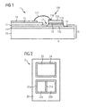
- FIG. 1 shows a cross-sectional view of a section of a luminous means, as it was produced by a method according to the proposed principle.
- the luminous means 1 is applied to a carrier 10 a serving as a heat sink.
- This support comprises a continuous copper core 10, which has sufficient stability and whose heat capacity is sufficiently large to dissipate the heat generated during operation by the luminous element 100.
- the copper core 10 moreover has the advantage that it can serve as the rear electrode for the luminous element 100.
- a ceramic substrate may also be used as a carrier with a metallized chip mounting area.
- the individual partial layers in the present exemplary embodiment comprise a partial layer of nickel 11 and a gold layer 12 applied thinly thereon.
- the gold layer 12 prevents undesired oxidation of the layers underneath and thus extends the service life.
- a dielectric layer 13 is applied in partial areas.
- contact tabs 14 are vapor-deposited, which later allow the bonding of the filament 100 via bonding wires 117.
- the partial layers 11 and 12 are structured in individual partial regions 17 in order to ensure a fixation of the luminous element 100 on a solder 15.
- This solder 15 is applied in a second subregion 12 a, which is surrounded by the structured subregions 17. As can be seen, the solder does not wet the structured partial regions 17, but only the second partial region 12a of the chip mounting region.
- the applied and fixed to the solder optoelectronic component is fixed in the second portion 12a.
- the luminous element 100 for example in the form of a light-emitting diode, comprises a rear-side mirror layer 115 for improving the light extraction.
- the luminous element may be formed as a thin-film light-emitting diode. Corresponding methods of production of such luminous bodies are known to the person skilled in the art, so that a further explanation is omitted.
- the luminous body 100 has on its surface a contact 116, which is fastened via a bonding wire 117 with a corresponding contact pad and a contact lug 14 on the surface of the luminous means and the dielectric layer 13.
- the structured first partial regions 17 are covered with a thin nickel oxide layer 16.
- This nickel oxide layer which is produced by the removal of the gold layer and subsequent oxidation, is solder-repellent, so that when applying solder material to the chip mounting area these sub-areas are not wetted.
- Various adhesion forces subsequently pull a luminous body applied to the solder into the areas with the most solder.
- the position of a luminous element within the chip mounting area can be determined precisely.
- the gold layer 12a is removed by a laser in this exemplary embodiment.
- a laser beam is directed onto the chip mounting region and guided along, so that the partial layer 12 evaporates at the points which the laser beam sweeps over and thus defines the partial regions 17.
- the additional energy introduced by the laser beam oxidizes with oxygen at the same time the underlying nickel layer 11, which then has the solder-repellent properties. If the solder is to be applied later, it must be ensured that a flux used does not again reduce the nickel oxide layer 16 in the structured subregions 17, thus canceling out the structuring again.
- the solder is applied, for example by a solder dispensing method.
- the applied luminous bodies 100 are fixed by the solder on the second portions 12 a and attached thereto.
- the electrical contacting with contact wires 117 to the luminous element or the optoelectronic component 100 can take place by a wire-bonding method.
- FIG. 2 shows a plan view to explain the different structuring options.
- the illustration shows a plan view of a chip mounting area that may form part of a larger carrier.
- the chip mounting area comprises two main areas, each of which in turn is structured into first and second partial areas.
- the chip mounting area is structured by a circumferential partial area 24, so that a surface 23 exposed therein is present. This forms the second subarea.
- On the surface can be applied via a dispensing, a deposition or a printing process solder material.
- the peripheral portion 24, however, has solder repellent properties, so that the solder material is concentrated in the area 23 substantially.
- a second main region of the structured chip mounting region is subdivided into two second subregions 22a and 22b, each separated by a structured web 21b are separated.
- the partial regions 22a and 22b are completely surrounded by a solder-deflecting first partial region 21a.
- Solder material which is deposited in the two second subregions 22a and 22b, remains separated by the structured web 21b, so that in this embodiment, for example, two separate optoelectronic components can be placed on the individual subregions 22a and 22b.
- the surfaces of the subregions 23 and 22a and 22b are metallic, so that the applied solder material on the one hand serves for heat dissipation in an operation of the optoelectronic component and on the other hand can simultaneously form a rearward electrical contact.
- the proposed structuring of the chip mounting region makes it possible to provide different geometrically arranged subregions in which optoelectronic components can be placed in a positionally accurate manner. This can improve overall etendue and the uniformity of the light emission.
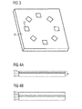
- FIG. 3 in this respect shows a section of a more complex chip mounting area, in which rectangular sections 31 are structured. These are arranged around a common center substantially circular. By a suitable wiring on the support, the optoelectronic components can be controlled individually and thus realize different lighting applications.
- Different size and shape of the subregions make it possible to provide different optoelectronic components and at the same time their different emission characteristics to take into account.
- mixed colors can also be produced by arranging suitable components adjacent to one another for light emission at different wavelengths. Since the first subarea of the chip mounting region, which has the solder-repelling property after structuring, can comprise very small layer thicknesses, components can also be placed sufficiently close to one another without a reduction in the light output or the emission quality during operation. It is even possible, by suitable choice of the thickness of the solder-deflecting first portion which separates two adjacent second portions, optoelectronic components directly adjacent to each other with a distance smaller than the thickness of the first portion to arrange and secure.
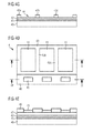
- FIGS. 4A to 4E show an embodiment of a method for manufacturing assemblies with optoelectronic devices.
- a support 4 serving as a heat sink is provided.
- This includes a copper core 40 which serves primarily as a heat sink, but may also include other materials.
- an insulating dielectric layer 41 is applied, which is a short circuit between the copper core 40th and prevent overlying electrically conductive layer 42.
- the dielectric layer 41 also has sufficient thermal conductivity here.
- the layer 42 comprises a plurality of metallization layers, which are not shown in greater detail here for reasons of clarity.
- a metallization of copper is first applied to the dielectric layer 41.
- nickel is vapor-deposited onto these and, in turn, a thin gold layer is applied to prevent oxidation.
- the nickel layer disposed between copper and gold is necessary to prevent diffusion of the gold into the copper layer and subsequent oxidation of the copper layer.
- other materials can be used. For example, partial layers of copper and silver or nickel and silver are also suitable for attaching later-mounted luminous bodies.
- the dielectric layer 41 is a few micrometers thick, the overlying Kupfermetallmaschines GmbH may have a thickness of 35 microns to 70 microns or more, the nickel layer has a thickness of about 10 .mu.m to 20 microns.
- solder stop layer is now deposited on the sublayer 42 over a large area. The result is in FIG. 4B shown. Subsequently, the solder stop layer is patterned by means of a photomask method and subdivided into individual first subregions 43a, 43b and 43c.
- a solder-stop layer for example, a particularly insensitive photoresist, or other organic Layer. This should be stable at least until the manufacture of the component is completed.
- the now unexposed part of the photoresist layer acting as a solder stop layer is removed and thus second subregions 44 are defined. After removal of the unexposed areas, the surface of the metallization layer 42 is exposed again.
- Figure 4D shows a section of a carrier in plan view to illustrate the individual structured first and second portions 43a, 43b, 43c and 44.
- the section along the axis I'-I corresponds to the cross-sectional view according to FIG. 4C , In the second subregions 44, the metallic surface is exposed.
- contact pads 45 are additionally exposed, which are surrounded by a dielectric protective layer 46.
- the cross-sectional view along the line II'-II is in Figure 4E shown.
- a further dielectric layer 47 is applied for electrical insulation.
- this layer 47 can also be formed by the solder stop layer, provided that it acts electrically insulating.
- the contact elements 45 are deposited as contact lugs and contact pads. To prevent oxidation of the contact pads and reduction of a short circuit probability, these are surrounded by a further dielectric protective layer 46.
- the contact lugs for supplying electrical energy to the contact pads 45 are covered by the protective layer 46 in the illustrated embodiment.
- contact pads 45 are exposed, which are connected, for example, via a bonding wire connection with the optoelectronic components in the subregions 44.
- 47 contact holes are provided in the dielectric layer, which allow electrical contact with the metallic layer 42 and thus the optoelectronic components in the sub-regions 44.
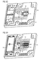
- FIGS. 5A to 5D show a further embodiment of a method for the production of bulbs.
- a carrier 50 serving as a heat sink for example, a copper core, a ceramic core, a PCB, a leadframe, or a similar carrier having high thermal conductivity is covered with metal electrically conductive layers in a chip mounting region 51 and in a wire bond region 52.
- the wire-bond region 52 and the chip mounting region 51 are in an electrically conductive contact.
- the other existing recesses on serving as a heat sink carrier provide fasteners with which the later manufactured device can be attached to other elements.
- FIG. 5B shows a thin circuit board for modular construction with the corresponding recesses in laminate technology.
- the thin printed circuit board 50a comprises a plastic in which different contact lines 55 and 58 are incorporated in one or more layers.
- contact elements 54, 54a, 56, 56a and 57 are arranged on the surface of the thin printed circuit board. These are exposed, while the contact lines 55 may be coated with a thin protective layer to protect against damage.
- the contact elements include, for example a copper layer or a thin copper-nickel-gold metallization layer.
- Some of the contact lugs 57 are connected via leads 55 to the contact lugs 54.
- a central recess 53 is provided, which provides a later access to the structured chip mounting region 51 and the structured wire bond region 52 according to FIG FIG. 5A allows.
- the further contact elements 56a, 56 and 57 can be equipped with various components in SMD technology.
- the thin circuit board is mounted on the heat sink serving carrier 50, for example, laminated.
- the carrier 50 it may be expedient to apply a thin lacquer layer on the carrier 50 with the recess of the chip mounting region 51 and of the wire bond region 52 before lamination.
- the carrier continues to act as a heat sink.
- the contact elements 54 are now arranged adjacent to the recess and the structured chip mounting region 51.
- Another contact 54a is adjacent to the patterned wire bond region 52 of the carrier 50.
- solder paste is then applied by Lotdispens vide on the structured chip mounting region 51. Leakage of the solder is prevented by the structuring of the chip mounting area and the division into first and second partial areas, the first partial areas of the chip mounting area having solder-repelling properties. As a result, the applied solder material wets only the second portions. Subsequently, the semiconductor devices 60 become on the chip mounting area arranged. By adhesive forces the solder paste forces the individual optoelectronic components in the respective second sub-areas, resulting in the in the FIG. 5D illustrated regular arrangement results.
- the lamination of the thin-film plate was carried out before the application of the solder and the optoelectronic components.
- this is not mandatory. It is also possible, first by means of various methods, e.g. Lotdispensmaschine or printing process to apply solder material on the chip mounting area and thus to attach the optoelectronic devices. Subsequently, the thin-film plate is then attached to the carrier.
- the chip mounting area is divided into six rectangular second partial areas.
- the individual contact pads 54 are connected via bond wires to the contact pads on the optoelectronic components 60.
- the structured wire bond region 52 is connected via contact wires to the contact pad 54a on the laminate carrier.
- solder material can be deposited on the further contact pads by means of a solder dispensing method, and later SMD components 59c, 59b or chip components 59a can be attached.
- An applied guard ring 61 surrounds the contact pads 54, 54a and the recessed area with the chip mounting area and the wire bond areas 51 and 52 respectively. Through the guard ring 61 it is also possible to solder the contact pads 56, 57 and 56a instead of with Lotdispenshabilit also otherwise, for example, screen printing or stencil printing, apply.
- optoelectronic components and, in general, luminous bodies can be fastened at previously well-defined positions by means of a solder material. This improves the positioning of individual components within a large chip mounting area.
- the first portion is solder repellent, i. H.
- An applied solder material does not wet this portion. Accordingly, when optoelectronic components are arranged on the solder material, they are drawn through the solder material into the second subregion and fixed there. Structuring can be carried out, for example, by appropriate application of solder stop layers. Alternatively, it is also possible to remove or oxidize metal layers already located on the support serving as a heat sink in the chip mounting region, so that they have solder-resisting properties. Especially the latter enables particularly fine and narrow structures using laser structuring techniques.
Applications Claiming Priority (2)
| Application Number | Priority Date | Filing Date | Title |
|---|---|---|---|
| DE102008063325A DE102008063325A1 (de) | 2008-12-30 | 2008-12-30 | Verfahren zur Fertigung von Leuchtmitteln |
| EP09771691.4A EP2371000B1 (de) | 2008-12-30 | 2009-11-27 | Verfahren zur fertigung von leuchtmitteln |
Related Parent Applications (2)
| Application Number | Title | Priority Date | Filing Date |
|---|---|---|---|
| EP09771691.4 Division | 2009-11-27 | ||
| EP09771691.4A Division-Into EP2371000B1 (de) | 2008-12-30 | 2009-11-27 | Verfahren zur fertigung von leuchtmitteln |
Publications (1)
| Publication Number | Publication Date |
|---|---|
| EP2544234A1 true EP2544234A1 (de) | 2013-01-09 |
Family
ID=41725366
Family Applications (2)
| Application Number | Title | Priority Date | Filing Date |
|---|---|---|---|
| EP12186956A Withdrawn EP2544234A1 (de) | 2008-12-30 | 2009-11-27 | Verfahren zur Fertigung einer lichtemittierenden Vorrichtung |
| EP09771691.4A Active EP2371000B1 (de) | 2008-12-30 | 2009-11-27 | Verfahren zur fertigung von leuchtmitteln |
Family Applications After (1)
| Application Number | Title | Priority Date | Filing Date |
|---|---|---|---|
| EP09771691.4A Active EP2371000B1 (de) | 2008-12-30 | 2009-11-27 | Verfahren zur fertigung von leuchtmitteln |
Country Status (7)
| Country | Link |
|---|---|
| US (1) | US8809082B2 (ja) |
| EP (2) | EP2544234A1 (ja) |
| JP (1) | JP5766122B2 (ja) |
| KR (1) | KR101681343B1 (ja) |
| CN (1) | CN102272925B (ja) |
| DE (1) | DE102008063325A1 (ja) |
| WO (1) | WO2010075831A1 (ja) |
Cited By (1)
| Publication number | Priority date | Publication date | Assignee | Title |
|---|---|---|---|---|
| DE102013215588A1 (de) * | 2013-08-07 | 2015-02-12 | Brose Fahrzeugteile GmbH & Co. Kommanditgesellschaft, Würzburg | Leiterplattenanordnung, Steuervorrichtung für ein Kühlerlüftermodul und Verfahren |
Families Citing this family (9)
| Publication number | Priority date | Publication date | Assignee | Title |
|---|---|---|---|---|
| DE102008063325A1 (de) | 2008-12-30 | 2010-07-01 | Osram Opto Semiconductors Gmbh | Verfahren zur Fertigung von Leuchtmitteln |
| US8816481B2 (en) * | 2011-11-04 | 2014-08-26 | Panasonic Corporation | Semiconductor device having a porous nickel plating part |
| DE102012215705B4 (de) * | 2012-09-05 | 2021-09-23 | OSRAM Opto Semiconductors Gesellschaft mit beschränkter Haftung | Gehäuse für ein optisches bauelement, baugruppe, verfahren zum herstellen eines gehäuses und verfahren zum herstellen einer baugruppe |
| ITTR20120012A1 (it) * | 2012-11-20 | 2013-02-19 | Tecnologie E Servizi Innovativi T S I S R L | Mpcb-led-sink20 - circuito stampato su base metallica con trasferimento diretto del calore dal pad termico dei led di potenza allo strato metallico della mpcb con capacita' di abbassare la temperatura della giunzione del led di ulteriori 20 °c rispet |
| DE102013201775A1 (de) * | 2013-02-04 | 2014-08-07 | Osram Gmbh | Beleuchtungsmodul und Verfahren zur Herstellung eines Beleuchtungsmoduls |
| DE102013101262A1 (de) | 2013-02-08 | 2014-08-14 | Osram Opto Semiconductors Gmbh | Optoelektronisches Leuchtmodul, optoelektronische Leuchtvorrichtung und Kfz-Scheinwerfer |
| US9215794B2 (en) * | 2013-05-06 | 2015-12-15 | Shenzhen China Star Optoelectronics Technology Co., Ltd. | Circuit board and display device |
| JP2015176975A (ja) * | 2014-03-14 | 2015-10-05 | パナソニックIpマネジメント株式会社 | 半導体装置 |
| CN109188631B (zh) * | 2018-09-26 | 2022-06-24 | 昂纳信息技术(深圳)有限公司 | 一种尾纤的防脱落方法及光学装置 |
Citations (6)
| Publication number | Priority date | Publication date | Assignee | Title |
|---|---|---|---|---|
| WO2005043966A1 (de) * | 2003-11-03 | 2005-05-12 | Eupec | Lötstopbarriere |
| DE102005031336A1 (de) * | 2005-05-13 | 2006-11-16 | Osram Opto Semiconductors Gmbh | Projektionseinrichtung |
| WO2008040307A2 (de) * | 2006-09-25 | 2008-04-10 | Osram Opto Semiconductors Gmbh | Verfahren zur herstellung einer anordnung optoelektronischer bauelemente und anordnung optoelektronischer bauelemente |
| US20080206928A1 (en) * | 2007-02-26 | 2008-08-28 | Fuji Electric Device Technology Co., Ltd. | Soldering method and method of manufacturing semiconductor device including soldering method |
| DE102008001221A1 (de) * | 2007-04-24 | 2008-10-30 | Ceramtec Ag | Bauteil mit einem keramischen Körper mit metallisierter Oberfläche |
| DE102008063325A1 (de) | 2008-12-30 | 2010-07-01 | Osram Opto Semiconductors Gmbh | Verfahren zur Fertigung von Leuchtmitteln |
Family Cites Families (11)
| Publication number | Priority date | Publication date | Assignee | Title |
|---|---|---|---|---|
| DE2528000B2 (de) * | 1975-06-24 | 1979-12-20 | Licentia Patent-Verwaltungs-Gmbh, 6000 Frankfurt | Verfahren zur Herstellung einer Lötfläche relativ großer Abmessungen |
| US6546620B1 (en) * | 2000-06-29 | 2003-04-15 | Amkor Technology, Inc. | Flip chip integrated circuit and passive chip component package fabrication method |
| US6660559B1 (en) * | 2001-06-25 | 2003-12-09 | Amkor Technology, Inc. | Method of making a chip carrier package using laser ablation |
| DE102004016697B4 (de) * | 2004-02-27 | 2007-10-11 | Osram Opto Semiconductors Gmbh | Verfahren zum Herstellen von Halbleiterchips umfassend ein Verbindungsverfahren, das Löten mit einem Lot umfasst, und Halbleiterchip |
| EP1575084B1 (en) * | 2004-03-01 | 2010-05-26 | Imec | Method for depositing a solder material on a substrate |
| CN100571353C (zh) | 2005-05-13 | 2009-12-16 | 奥斯兰姆奥普托半导体有限责任公司 | 投影设备 |
| KR100658939B1 (ko) | 2005-05-24 | 2006-12-15 | 엘지전자 주식회사 | 발광 소자의 패키지 |
| US20060289887A1 (en) | 2005-06-24 | 2006-12-28 | Jabil Circuit, Inc. | Surface mount light emitting diode (LED) assembly with improved power dissipation |
| KR100699161B1 (ko) | 2005-10-06 | 2007-03-22 | 엘지전자 주식회사 | 발광 소자 패키지 및 그의 제조 방법 |
| KR20080007961A (ko) | 2006-07-19 | 2008-01-23 | 알티전자 주식회사 | 엘이디 모듈의 냉각 장치 및 그 제조 방법 |
| CN101154656B (zh) * | 2006-09-30 | 2010-05-12 | 香港微晶先进封装技术有限公司 | 多芯片发光二极管模组结构及其制造方法 |
-
2008
- 2008-12-30 DE DE102008063325A patent/DE102008063325A1/de not_active Withdrawn
-
2009
- 2009-11-27 WO PCT/DE2009/001693 patent/WO2010075831A1/de active Application Filing
- 2009-11-27 KR KR1020117017729A patent/KR101681343B1/ko active IP Right Grant
- 2009-11-27 EP EP12186956A patent/EP2544234A1/de not_active Withdrawn
- 2009-11-27 EP EP09771691.4A patent/EP2371000B1/de active Active
- 2009-11-27 JP JP2011543974A patent/JP5766122B2/ja active Active
- 2009-11-27 US US13/142,391 patent/US8809082B2/en active Active
- 2009-11-27 CN CN200980153425.3A patent/CN102272925B/zh active Active
Patent Citations (6)
| Publication number | Priority date | Publication date | Assignee | Title |
|---|---|---|---|---|
| WO2005043966A1 (de) * | 2003-11-03 | 2005-05-12 | Eupec | Lötstopbarriere |
| DE102005031336A1 (de) * | 2005-05-13 | 2006-11-16 | Osram Opto Semiconductors Gmbh | Projektionseinrichtung |
| WO2008040307A2 (de) * | 2006-09-25 | 2008-04-10 | Osram Opto Semiconductors Gmbh | Verfahren zur herstellung einer anordnung optoelektronischer bauelemente und anordnung optoelektronischer bauelemente |
| US20080206928A1 (en) * | 2007-02-26 | 2008-08-28 | Fuji Electric Device Technology Co., Ltd. | Soldering method and method of manufacturing semiconductor device including soldering method |
| DE102008001221A1 (de) * | 2007-04-24 | 2008-10-30 | Ceramtec Ag | Bauteil mit einem keramischen Körper mit metallisierter Oberfläche |
| DE102008063325A1 (de) | 2008-12-30 | 2010-07-01 | Osram Opto Semiconductors Gmbh | Verfahren zur Fertigung von Leuchtmitteln |
Cited By (2)
| Publication number | Priority date | Publication date | Assignee | Title |
|---|---|---|---|---|
| DE102013215588A1 (de) * | 2013-08-07 | 2015-02-12 | Brose Fahrzeugteile GmbH & Co. Kommanditgesellschaft, Würzburg | Leiterplattenanordnung, Steuervorrichtung für ein Kühlerlüftermodul und Verfahren |
| US10028384B2 (en) | 2013-08-07 | 2018-07-17 | Brose Fahrzeugteile Gmbh & Co. Kg, Wuerzburg | Circuit board assembly, control device for a cooler fan module and method |
Also Published As
| Publication number | Publication date |
|---|---|
| CN102272925A (zh) | 2011-12-07 |
| JP5766122B2 (ja) | 2015-08-19 |
| US20120107973A1 (en) | 2012-05-03 |
| KR101681343B1 (ko) | 2016-11-30 |
| DE102008063325A1 (de) | 2010-07-01 |
| EP2371000B1 (de) | 2016-10-26 |
| CN102272925B (zh) | 2014-01-01 |
| KR20110100307A (ko) | 2011-09-09 |
| WO2010075831A1 (de) | 2010-07-08 |
| JP2012514340A (ja) | 2012-06-21 |
| EP2371000A1 (de) | 2011-10-05 |
| US8809082B2 (en) | 2014-08-19 |
Similar Documents
| Publication | Publication Date | Title |
|---|---|---|
| EP2371000B1 (de) | Verfahren zur fertigung von leuchtmitteln | |
| EP1328976B1 (de) | Led-modul | |
| DE102008063757B4 (de) | Halbleiterbauteil | |
| EP2297780B1 (de) | Optoelektronisches modul mit einem trägersubstrat und einer mehrzahl von strahlung emittierenden halbleiterbauelementen und verfahren zu dessen herstellung | |
| EP2223337B1 (de) | Optoelektronisches bauelement und herstellungsverfahren für ein optoelektronisches bauelement | |
| DE2744167C2 (de) | Optoelektronisches Koppelelement | |
| DE19757850A1 (de) | Lichtemittierendes Anzeigeelement, Verfahren zum Verbinden desselben mit einem elektrischen Verdrahtungssubstrat und Herstellungsverfahren hierfür | |
| DE112011100376T5 (de) | Verfahren zur herstellung einer licht aussendenden vorrichtung und licht aussendende vorrichtung | |
| DE112008004155T5 (de) | Verfahren zum Herstellen eines Substrats für eine Baugruppe mit lichtemittierendem Elementsowie Baugruppe mit lichtemittierendem Element unter Verwendung eines derartigen Substrats | |
| DE10148120A1 (de) | Elektronische Bauteile mit Halbleiterchips und ein Systemträger mit Bauteilpositionen sowie Verfahren zur Herstellung derselben | |
| DE102006015117A1 (de) | Optoelektronischer Scheinwerfer, Verfahren zum Herstellen eines optoelektronischen Scheinwerfers und Lumineszenzdiodenchip | |
| EP2223354B1 (de) | Optoelektronisches bauelement | |
| EP2044363A1 (de) | Strahlungsemittierende einrichtung mit mehreren strahlungsemittierenden bauelementen und beleuchtungseinrichtung | |
| DE102004019431A1 (de) | Hybrider Leiterplattenaufbau zur kompakten Aufbautechnik von elektrischen Bauelementen | |
| DE102006015115A1 (de) | Elektronisches Modul und Verfahren zum Herstellen eines elektronischen Moduls | |
| WO2017148899A1 (de) | Modul für eine leuchte | |
| WO2024079183A1 (de) | Verfahren zum herstellen eines bauelements und bauelement | |
| EP2067390A2 (de) | Verfahren zur herstellung einer anordnung optoelektronischer bauelemente und anordnung optoelektronischer bauelemente | |
| DE102017105017A1 (de) | Herstellung von strahlungsemittierenden bauelementen | |
| DE102013218268A1 (de) | Träger und Leuchtvorrichtung | |
| WO2017129697A1 (de) | Optoelektronisches bauelement mit seitenkontakten | |
| DE10148043A1 (de) | Elektronisches Bauteil mit einem Kunststoffgehäuse und Komponenten eines Systemträgers und Verfahren zu deren Herstellung | |
| DE102022110031A1 (de) | Herstellungsverfahren, optoelektronisches halbleiterbauteil und träger | |
| DE102022108571A1 (de) | Zusammensetzung, verfahren zum verbinden eines trägers und einer elektronischen komponente und elektronisches bauelement | |
| WO2024052301A1 (de) | Verfahren zum erzeugen von leiterbahnen und transparente verbundscheibe |
Legal Events
| Date | Code | Title | Description |
|---|---|---|---|
| PUAI | Public reference made under article 153(3) epc to a published international application that has entered the european phase |
Free format text: ORIGINAL CODE: 0009012 |
|
| STAA | Information on the status of an ep patent application or granted ep patent |
Free format text: STATUS: THE APPLICATION HAS BEEN PUBLISHED |
|
| AC | Divisional application: reference to earlier application |
Ref document number: 2371000 Country of ref document: EP Kind code of ref document: P |
|
| AK | Designated contracting states |
Kind code of ref document: A1 Designated state(s): AT BE BG CH CY CZ DE DK EE ES FI FR GB GR HR HU IE IS IT LI LT LU LV MC MK MT NL NO PL PT RO SE SI SK SM TR |
|
| STAA | Information on the status of an ep patent application or granted ep patent |
Free format text: STATUS: THE APPLICATION IS DEEMED TO BE WITHDRAWN |
|
| 18D | Application deemed to be withdrawn |
Effective date: 20130710 |