EP2544232A1 - Light emitting device array and backlight unit - Google Patents
Light emitting device array and backlight unit Download PDFInfo
- Publication number
- EP2544232A1 EP2544232A1 EP12159814A EP12159814A EP2544232A1 EP 2544232 A1 EP2544232 A1 EP 2544232A1 EP 12159814 A EP12159814 A EP 12159814A EP 12159814 A EP12159814 A EP 12159814A EP 2544232 A1 EP2544232 A1 EP 2544232A1
- Authority
- EP
- European Patent Office
- Prior art keywords
- emitting device
- light emitting
- light
- guide plate
- region
- Prior art date
- Legal status (The legal status is an assumption and is not a legal conclusion. Google has not performed a legal analysis and makes no representation as to the accuracy of the status listed.)
- Granted
Links
Images


Classifications
-
- G—PHYSICS
- G02—OPTICS
- G02F—OPTICAL DEVICES OR ARRANGEMENTS FOR THE CONTROL OF LIGHT BY MODIFICATION OF THE OPTICAL PROPERTIES OF THE MEDIA OF THE ELEMENTS INVOLVED THEREIN; NON-LINEAR OPTICS; FREQUENCY-CHANGING OF LIGHT; OPTICAL LOGIC ELEMENTS; OPTICAL ANALOGUE/DIGITAL CONVERTERS
- G02F1/00—Devices or arrangements for the control of the intensity, colour, phase, polarisation or direction of light arriving from an independent light source, e.g. switching, gating or modulating; Non-linear optics
- G02F1/01—Devices or arrangements for the control of the intensity, colour, phase, polarisation or direction of light arriving from an independent light source, e.g. switching, gating or modulating; Non-linear optics for the control of the intensity, phase, polarisation or colour
- G02F1/13—Devices or arrangements for the control of the intensity, colour, phase, polarisation or direction of light arriving from an independent light source, e.g. switching, gating or modulating; Non-linear optics for the control of the intensity, phase, polarisation or colour based on liquid crystals, e.g. single liquid crystal display cells
- G02F1/133—Constructional arrangements; Operation of liquid crystal cells; Circuit arrangements
- G02F1/1333—Constructional arrangements; Manufacturing methods
- G02F1/1335—Structural association of cells with optical devices, e.g. polarisers or reflectors
- G02F1/1336—Illuminating devices
-
- G—PHYSICS
- G02—OPTICS
- G02B—OPTICAL ELEMENTS, SYSTEMS OR APPARATUS
- G02B6/00—Light guides; Structural details of arrangements comprising light guides and other optical elements, e.g. couplings
- G02B6/0001—Light guides; Structural details of arrangements comprising light guides and other optical elements, e.g. couplings specially adapted for lighting devices or systems
- G02B6/0011—Light guides; Structural details of arrangements comprising light guides and other optical elements, e.g. couplings specially adapted for lighting devices or systems the light guides being planar or of plate-like form
- G02B6/0081—Mechanical or electrical aspects of the light guide and light source in the lighting device peculiar to the adaptation to planar light guides, e.g. concerning packaging
- G02B6/0086—Positioning aspects
- G02B6/0091—Positioning aspects of the light source relative to the light guide
-
- G—PHYSICS
- G02—OPTICS
- G02B—OPTICAL ELEMENTS, SYSTEMS OR APPARATUS
- G02B6/00—Light guides; Structural details of arrangements comprising light guides and other optical elements, e.g. couplings
- G02B6/0001—Light guides; Structural details of arrangements comprising light guides and other optical elements, e.g. couplings specially adapted for lighting devices or systems
- G02B6/0011—Light guides; Structural details of arrangements comprising light guides and other optical elements, e.g. couplings specially adapted for lighting devices or systems the light guides being planar or of plate-like form
- G02B6/0066—Light guides; Structural details of arrangements comprising light guides and other optical elements, e.g. couplings specially adapted for lighting devices or systems the light guides being planar or of plate-like form characterised by the light source being coupled to the light guide
- G02B6/0068—Arrangements of plural sources, e.g. multi-colour light sources
-
- G—PHYSICS
- G02—OPTICS
- G02F—OPTICAL DEVICES OR ARRANGEMENTS FOR THE CONTROL OF LIGHT BY MODIFICATION OF THE OPTICAL PROPERTIES OF THE MEDIA OF THE ELEMENTS INVOLVED THEREIN; NON-LINEAR OPTICS; FREQUENCY-CHANGING OF LIGHT; OPTICAL LOGIC ELEMENTS; OPTICAL ANALOGUE/DIGITAL CONVERTERS
- G02F1/00—Devices or arrangements for the control of the intensity, colour, phase, polarisation or direction of light arriving from an independent light source, e.g. switching, gating or modulating; Non-linear optics
- G02F1/01—Devices or arrangements for the control of the intensity, colour, phase, polarisation or direction of light arriving from an independent light source, e.g. switching, gating or modulating; Non-linear optics for the control of the intensity, phase, polarisation or colour
- G02F1/13—Devices or arrangements for the control of the intensity, colour, phase, polarisation or direction of light arriving from an independent light source, e.g. switching, gating or modulating; Non-linear optics for the control of the intensity, phase, polarisation or colour based on liquid crystals, e.g. single liquid crystal display cells
- G02F1/133—Constructional arrangements; Operation of liquid crystal cells; Circuit arrangements
- G02F1/1333—Constructional arrangements; Manufacturing methods
- G02F1/1335—Structural association of cells with optical devices, e.g. polarisers or reflectors
- G02F1/1336—Illuminating devices
- G02F1/133602—Direct backlight
- G02F1/133611—Direct backlight including means for improving the brightness uniformity
-
- G—PHYSICS
- G02—OPTICS
- G02B—OPTICAL ELEMENTS, SYSTEMS OR APPARATUS
- G02B6/00—Light guides; Structural details of arrangements comprising light guides and other optical elements, e.g. couplings
- G02B6/0001—Light guides; Structural details of arrangements comprising light guides and other optical elements, e.g. couplings specially adapted for lighting devices or systems
- G02B6/0011—Light guides; Structural details of arrangements comprising light guides and other optical elements, e.g. couplings specially adapted for lighting devices or systems the light guides being planar or of plate-like form
- G02B6/0066—Light guides; Structural details of arrangements comprising light guides and other optical elements, e.g. couplings specially adapted for lighting devices or systems the light guides being planar or of plate-like form characterised by the light source being coupled to the light guide
- G02B6/0073—Light emitting diode [LED]
Abstract
Description
- This application claims the priority benefit of Korean Patent Application No.
10-2011-0067408, filed on July 7, 2011 - Embodiments relate to a light emitting device array and a backlight unit.
- Light Emitting Diodes (LEDs) are devices that convert electrical signals into light using characteristics of compound semiconductors and are used in home appliances, remote controls, electronic scoreboards, displays, various automated devices, and the like and the application range of LEDs continues to expand.
- A backlight unit which employs LEDs may be used in a display device such as a liquid crystal display device and may also be used in lighting devices in other fields. A generally used backlight unit includes a light source, a light guide plate that diffuses light generated by the light source, and optical sheets that function to spread or focus light emitted from the light guide plate.
- LEDs that are driven at low voltage and are highly efficient may be applied as the light source of the backlight unit. The LED is a 2-terminal diode including a compound semiconductor such as gallium arsenide (GaAs), Gallium Nitride (GaN), or indium gallium nitride (InGaN). When voltage is applied to the cathode and anode terminals of the LED, the LED emits visual light with light energy generated when electrons and holes are combined.
- The backlight unit is classified into an edge type and a direct type depending on the position of the light source.
- Edge type backlight units are generally applied to relatively small liquid crystal display devices such as monitors of laptop computers and desktop computers and have advantages in that the backlight units provide highly uniform light and have a long life and also contribute to achieving a slim liquid crystal display device.
- When a backlight unit employing light emitting devices is configured, there is a need to guide light generated by the light emitting devices in a specific direction and to guarantee uniform emission over the display area of the backlight unit. In addition, it is also an important issue to achieve a slim and light backlight unit in order to improve productivity and increase user convenience.
- In one embodiment, a light emitting device array includes a substrate including a first region and a second region that is inclined with respect to the first region, a first light emitting device package arranged on the first region, and at least one second light emitting device package that is arranged on the second region and is inclined with respect to the first light emitting device package at an inclination angle between 90° and 160°.
- In another embodiment, a backlight unit includes a light guide plate, and at least one light emitting device array arranged adj acent to a corner of the light guide plate which corresponds to an edge of one side surface of the light guide plate, the light emitting device array comprising a substrate including a first region and a second region that is inclined with respect to the first region, a first light emitting device package arranged on the first region, and at least one second light emitting device package that is arranged on the second region and is inclined with respect to the first light emitting device package at an inclination angle between 90° and 160°.
- Details of embodiments will be more clearly understood from the following detailed description taken in conjunction with the accompanying drawings, in which:
-
FIG. 1 is an exploded perspective view schematically illustrating a light emitting device module including an array of light emitting devices according to an embodiment; -
FIG. 2 is a perspective view of a first light emitting device package shown inFIG. 1 ; -
FIG. 3 is an enlarged view of a first embodiment of a 'P' block shown inFIG. 1 ; -
FIG. 4 is an enlarged view of a second embodiment of the 'P' block shown inFIG. 1 ; -
FIG. 5 illustrates a light emitting device array according to another embodiment; -
FIG. 6A is an exploded perspective view of a backlight unit according to one embodiment; -
FIGS. 6A to 6E are partial cross-sectional views of the backlight unit according to an embodiment; -
FIG. 7A is a partial cross-sectional view of a backlight unit according to an embodiment; -
FIG. 7B is a partial cross-sectional view of a backlight unit according to an embodiment; -
FIG. 7C is a partial cross-sectional view of a backlight unit according to an embodiment; -
FIG. 8 is a perspective exploded view of a liquid crystal display device including a backlight unit according to an embodiment; and -
FIG. 9 is a cross-sectional view of an electronic device including a backlight unit (not shown) according to an embodiment. - In the description of the embodiments, it will be understood that, when a layer (or film), a region, a pattern, or a structure is referred to as being "on" or "under" another substrate, another layer (or film), another region, another pad, or another pattern, it can be "directly" or "indirectly" over the other substrate, layer (or film), region, pad, or pattern, or one or more intervening layers may also be present. Such a position of the layer has been described with reference to the drawings.
- In the drawings, the thickness or size of each layer is exaggerated, omitted, or schematically illustrated for convenience of description and clarity. Also, the size of each constituent element does not entirely reflect the actual size thereof.
- Reference will now be made in detail to embodiments, examples of which are illustrated in the accompanying drawings.
-
FIG. 1 is an exploded perspective view schematically illustrating a light emitting device module including an array of light emitting devices according to an embodiment. - As shown in
FIG. 1 , a lightemitting device module 200 includes apower control module 210, a lightemitting device array 100, and aconnector 130. - The
power control module 210 may include apower supply 212 that generates power that is consumed by a first lightemitting device package 110 embedded in the lightemitting device array 100, acontrol unit 214 that controls operation of thepower supply 212, and aconnector connection portion 216 connected to one end of theconnector 130. - Here, the
power supply 212 operates under control of thecontrol unit 214 and generates power that is consumed by the lightemitting device array 100. - The
control unit 214 may control operation of thepower supply 212 according to an externally input command. - The externally input command may be, but is not limited to, a command output from an input device (not shown) directly connected to the light
emitting device module 200 or a command output from a remote control that is used to control operation of an apparatus including the lightemitting device module 200. - The
connector connection portion 216 is connected to one end of theconnector 130 and may provide power supplied from thepower supply 212 to theconnector 130. - The light
emitting device array 100 may include a first lightemitting device package 110 and a plurality of second lightemitting device packages 111 to 116, asubstrate 120, on which the first lightemitting device package 110 and the plurality of second lightemitting device packages 111 to 116 are provided, and aconnector terminal 122 that is formed on thesubstrate 120 and is connected to the other end of theconnector 130. - Here, the
connector terminal 122 may be electrically connected to theconnector connection portion 216 through theconnector 130. - The
substrate 120 may be a printed circuit board (PCB), a flexible printed circuit board, or a metal board. When thesubstrate 120 is a PCB, thesubstrate 120 may be a single-sided PCB, a double-sided PCB, a multi-layer PCB, or the like. The embodiments will be described below with reference to an example in which thesubstrate 120 is a single-sided PCB although thesubstrate 120 is not limited to the single-sided PCB. - The first and the plurality of second light
emitting device packages 110 to 116 may be, but are not necessarily, divided into a plurality of groups (not shown) and may be, but are not necessarily, connected in series or in parallel. - Although the number of the first and the plurality of second light
emitting device packages 110 to 116 shown inFIG. 1 is 7, there is no limitation as to the total number of the first and the plurality of second lightemitting device packages 110 to 116. - At least two of the first and the plurality of second light
emitting device packages 110 to 116 may, but not necessarily, emit light of different colors or light of the same color. - For example, in the case in which the first and the plurality of second light
emitting device packages 110 to 116 emit white light, the first and the plurality of second lightemitting device packages 110 to 116 may be implemented using light emitting device packages that emit red light and light emitting device packages that emit blue light. Thus, light emitting device packages that emit red light and light emitting device packages that emit blue light may be alternately mounted. The first and the plurality of second lightemitting device packages 110 to 116 that emit white light may also be implemented using light emitting device packages that emit red light, light emitting device packages that emit blue light, and light emitting device packages that emit green light. - The first and the plurality of second light
emitting device packages 110 to 116 may, but not necessarily, have the same configuration and at least one thereof may, but not necessarily, include a plurality of light emitting devices (not shown). Each of the first and the plurality of second lightemitting device packages 110 to 116 may be a side view type of light emitting device package that emits light from the side surfaces thereof. - The following description is given with reference to the case in which the first and the plurality of second light emitting device packages 110 to 116 have the same configuration.
-
FIG. 2 is a perspective view of the first light emitting device package shown inFIG. 1 . - The first light emitting
device package 110 shown inFIG. 2 has the same configuration as the second light emitting device packages 111 to 116 and at least one of the color of a fluorescent substance of the first light emittingdevice package 110 and the color of light emitted from a light emitting device of the first light emittingdevice package 110 may be different from that of the second light emitting device packages 111 to 116. - The first light emitting
device package 110 may include alight emitting device 11 and abody 12 on which thelight emitting device 11 is provided. - The
body 12 may be formed of at least one of a resin substance such as polyphthalamide (PPA), silicon (Si), aluminum (Al), aluminum nitride (AlN), AlOx, liquid polymer, photo sensitive glass (PSG), polyamide 9T (PA9T), syndiotactic polystyrene (SPS), a metallic substance, sapphire (Al2O3), beryllium oxide (BeO), ceramic, and a printed circuit board (PCB). - The
body 12 may be, but is not necessarily, formed using injection molding, etching, and the like. - A top surface of the
body 12 may have various shapes that include, but are not limited to, a triangle, a rectangle, a polygon, and a circle. - The
body 12 may have a cavity s in which thelight emitting device 11 is arranged, a cross-sectional shape of the cavity s may be a cup, a concave bowl, or the like, and an inner surface of thebody 12 that defines the cavity s may be formed obliquely in a downward direction. - The cavity s may have various plane shapes that include, but are not limited to, a circle, a quadrangle, a polygon, and an oval.
- First and second lead frames 13 and 14 may be arranged on a lower surface of the
body 12 and the first and second lead frames 13 and 14 may include one or more substance or alloy from among, for example, titanium (Ti), copper (Cu), nickel (Ni), gold (Au), chrome (Cr), tantalum (Ta), platinum (Pt), tin (Sn), silver (Ag), phosphorous (P), aluminum (Al), indium (In), palladium (Pd), cobalt (Co), silicon (Si), germanium (Ge), hafnium (Hf), ruthenium (Ru), and iron (Fe). - Each of the first and second lead frames 13 and 14 may be, but is not necessarily, formed in a single layer or multi-layer structure.
- An inner surface of the
body 12 may be formed obliquely at an inclination angle with respect to one of the first and second lead frames 13 and 14 and a reflection angle of light emitted from thelight emitting device 11 may vary according to the inclination angle, thereby enabling control of the beam angle (or beam range) of externally emitted light. The degree of concentration of light externally emitted from thelight emitting device 11 increases as the beam angle of the externally emitted light decreases and decreases as the beam angle increases. - The inner surface of the
body 12 may, but is not necessarily, have a plurality of inclination angles. - The first and second lead frames 13 and 14 may be electrically connected to the
light emitting device 11 and connected respectively to positive and negative poles of an external power source (not shown) to supply power to thelight emitting device 11. - The
light emitting device 11 may be mounted on thefirst lead frame 13. Thelight emitting device 11 may be die-bonded to thefirst lead frame 13 and may be wire-bonded to thesecond lead frame 14 through a wire (not shown) to receive power from the first and second lead frames 13 and 14. - Here, the
light emitting device 11 may be, but is not limited to, wire-bonded or die-bonded to the first and second lead frames 13 and 14. - A cathode mark (not shown) may be formed on the
body 12. The cathode mark may serve to discriminate the poles of thelight emitting device 11, i.e., the poles of the first and second lead frames 13 and 14, to prevent confusion when electrically connecting the first and second lead frames 13 and 14. - The
light emitting device 11 may be a light emitting diode (LED). The LED may be, but is not necessarily, a color LED that emits, for example, red, green, blue, or white light or an ultraviolet (UV) LED that emits ultraviolet light. A plurality of light emittingdevices 11 may be mounted on thefirst lead frame 13 and at least one light emittingdevice 11 may be mounted on the first and second lead frames 13 and 14 although there is no limitation as to the number of thelight emitting devices 11 and the mounting position thereof. - The embodiments are described below with reference to the case in which the
light emitting device 11 is a blue light emitting device that emits blue light. - The
body 12 may include aresin substance 17 that fills the cavity s. That is, theresin substance 17 may be, but is not necessarily, formed in a double-molding structure or a triple-molding structure. - The
resin substance 17 may be formed in the shape of a film and may include at least one of a fluorescent substance and an optical diffusion substance and may also include a translucent substance that does not include a fluorescent substance and an optical diffusion substance although there is no limitation as to the shape and composition of theresin substance 17. - In an embodiment, the
resin substance 17 may include first and secondfluorescent substances resin substance 17. - Specifically, in the case in which the first light emitting
device package 110 emits white light, the first and secondfluorescent substances light emitting device 11 that emits blue light. - Although the embodiment has been described with reference to the case in which the
resin substance 17 includes the first and secondfluorescent substances resin substance 17 may include a fluorescent substance of single color which may be, but is not limited to, a yellow fluorescent substance. - In the case in which the
light emitting device 11 emits red or green light, the first light emittingdevice package 110 may include a mixture of a blue fluorescent substance and a green fluorescent substance or a mixture of a blue fluorescent substance and a red fluorescent substance to emit white light. -
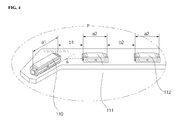
FIG. 3 is an enlarged view of a first embodiment of a 'P' block shown inFIG. 1 . - As shown in
FIG. 3 , the light emittingdevice array 100 according to an embodiment may include a first light emittingdevice package 110, a plurality of second light emitting device packages 111 and 112, and asubstrate 120 on which the first and the plurality of second light emitting device packages 110 to 112 are arranged. - The plurality of second light emitting device packages 110 to 112 may have the same package size and embodiments are described below with reference to the case in which the plurality of second light emitting device packages 110 to 112 have the same configuration.
- Here, the first light emitting
device package 110 may be arranged adjacent to one edge of thesubstrate 120. The edge may have a bent portion and the first light emittingdevice package 110 may be arranged obliquely according to the bent portion. - That is, the first light emitting
device package 110 may be inclined at an inclination angle θ with respect to the second light emittingdevice package 111 that is arranged adjacent to the first light emittingdevice package 110. - The inclination angle θ may be in a range of 90° to 160°. When the inclination angle θ is less than 90°, a beam range (or beam angle) (not shown) of light emitted from a light emitting surface of the first light emitting
device package 110 is directed toward side surfaces and light emitting surfaces of the plurality of second light emitting device packages 111 and 112, thus generating a dark zone at the edge. When the inclination angle θ is greater than 160°, the beam range (or beam angle) (not shown) of light emitted from the light emitting surface of the first light emittingdevice package 110 does not greatly differ from beam ranges (not shown) of the plurality of second light emitting device packages 111 and 112 and therefore it is not possible to reduce the total number of light emitting device packages arranged on thesubstrate 120. - Here, a first separation distance b1 between the first light emitting
device package 110 and the second light emittingdevice package 111 arranged adjacent thereto may be allowed to be equal to or longer than a second separation distance b2 between the plurality of second light emitting device packages 111 and 112. - That is, the first separation distance b1 may be changed according to the inclination angle θ and may be inversely proportional to the inclination angle θ.
- For example, the first separation distance b1 may be equal to the second separation distance b2 when the inclination angle θ is 160° and may be longer than the second separation distance b2 when the inclination angle θ is 90°.
- As described above, the second light emitting device packages 111 and 112 are spaced from each other by the second separation distance b2 and the separation distance between each of the second light emitting device packages 114, 115, and 116 may be equal to the second separation distance b2 as shown in
FIG. 1 . - When the light emitting device packages of the light emitting
device array 100 illustrated in the first embodiment have the same package size, the first separation distance b1 between the first and second light emitting device packages 110 and 111 may be changed according to the inclination angle θ between the first and second light emitting device packages 110 and 111. -
FIG. 4 is an enlarged view of a second embodiment of a 'P' block shown inFIG. 1 . - The same reference numbers as those of
FIG. 3 are used forFIG. 4 and portions of the second embodiment similar to the first embodiment are not described or are briefly described below. - As shown in
FIG. 4 , the light emittingdevice array 100 according to an embodiment may include a first light emittingdevice package 110, a plurality of second light emitting device packages 111 and 112, and asubstrate 120 on which the first light emittingdevice package 110 and the plurality of second light emitting device packages 111 and 112 are arranged. - Here, the first light emitting
device package 110 may have a different package size from the second light emitting device packages 111 and 112. - That is, the first light emitting
device package 110 may have a first package size a1 and the second light emitting device packages 111 and 112 may have a second package size a2 that is less than the first package size a1. - The first light emitting
device package 110 may be inclined at an inclination angle θ with respect to the second light emittingdevice package 111 that is arranged adjacent to thesubstrate 120. - The inclination angle θ may be in a range of 90° to 160°. When the inclination angle θ is less than 90°, a beam range (or beam angle) (not shown) of light emitted from a light emitting surface of the first light emitting
device package 110 is directed toward side surfaces and light emitting surfaces of the second light emitting device packages 111 and 112 to generate a blind zone at the edge. When the inclination angle θ is greater than 160°, the beam range (or beam angle) (not shown) of light emitted from the light emitting surface of the first light emittingdevice package 110 does not greatly differ from beam ranges (not shown) of the second light emitting device packages 111 and 112 and therefore it is not possible to reduce the total number of light emitting device packages arranged on thesubstrate 120. - Here, a first separation distance b1 between the first and second light emitting device packages 110 and 111 may be longer than a second separation distance b2 between the plurality of second light emitting device packages 111 and 112.
- That is, the first separation distance b1 may be changed according to the inclination angle θ and the first and second package sizes a1 and a2 and may be inversely proportional to the inclination angle θ and may be proportional to at least one of the first and second package sizes a1 and a2.
- However, the difference between the first and second separation distances b1 and b2 may be maximized when the inclination angle θ is 160° and may be minimized when the inclination angle θ is 90°.
- The second and third light emitting device packages 111 and 112 are spaced from each other by the second separation distance b2 and the separation distance between each of the fifth, sixth, and seventh light emitting device packages 114, 115, and 116 may be equal to the second separation distance b2 as shown in
FIG. 1 . - In the light emitting
device array 100 illustrated in the second embodiment, the first separation distance b1 between the first light emittingdevice package 110 having the first package size a1 and the second light emittingdevice package 111 that is adjacent to the first light emittingdevice package 110 and that has the second package size a2 may be changed according to the first package size a1 and the inclination angle θ. -
FIG. 5 illustrates a light emittingdevice array 200 according to another embodiment. - As shown in
FIG. 5 , the light emittingdevice array 200 according to this embodiment may include a first light emittingdevice package 210, a second light emittingdevice package 211, and asubstrate 220 on which the first light emittingdevice package 210 and the second light emittingdevice package 211 are arranged. - The
substrate 220 may include afirst region 222 and asecond region 224 that are formed in a bent shape and thefirst region 222 and thesecond region 224 may be inclined with respect to each other. - The first light emitting
device package 210 may be arranged on thefirst region 222 and the second light emittingdevice package 211 may be arranged on thesecond region 224. The first light emittingdevice package 210 and the second light emittingdevice package 211 which emit white light may be implemented using a light emitting device package that emits red light and a light emitting device package that emits blue light. Thus, light emitting device packages that emit red light and light emitting device packages that emit blue light may be alternately mounted. The light emitting device packages that emit white light may also be implemented using light emitting device packages that emit red light, light emitting device packages that emit blue light, and light emitting device packages that emit green light. - Each of the first and second light emitting device packages 210 and 211 may be of a top view type that emits light upwardly.
- The
substrate 220 may have a plurality of bent portions. When thesubstrate 220 has two bent portions, thesubstrate 220 may include a first region, a second region, and a third region and a light emitting device package may be arranged on each of the regions. -
FIG. 6A is an exploded perspective view of abacklight unit 300 according to one embodiment andFIGS. 6A to 6E are partial cross-sectional views of thebacklight unit 300 according to another embodiment. - As shown in
FIG. 6A , thebacklight unit 300 according to the embodiment is of an edge-light type and includes a light emittingdevice array 310 and alight guide plate 320. The light emittingdevice array 310 includes asubstrate 316 and a light emittingdevice array 310. Thesubstrate 316 is arranged adjacent to a corner (or corner edge) of thelight guide plate 320, which corresponds to an edge of one side surface of thelight guide plate 320, and has abent portion 314 so as to form an inclination angle in a range of 90° to 160°. The light emittingdevice array 310 includes light emitting device packages 312 that are arranged on a portion of thesubstrate 316 which faces thelight guide plate 320. - The
backlight unit 300 is a means for providing light to a liquid crystal display device (not shown) and may be located at the rear side of the liquid crystal display device (not shown). Thebacklight unit 300 may provide light with high brightness and an appropriate viewing angle to the liquid crystal display device (not shown). - The light emitting device packages 312 may be provided on the
substrate 316. The light emitting device packages 312 may be electrically connected to thesubstrate 316. The light emitting device packages 312 may receive power from the outside and generate and provide light to thelight guide plate 320. Although the light emitting device packages 312 may be provided in one array on thesubstrate 316, there is no limitation as to how the light emitting device packages 312 are arrayed on thesubstrate 316 and the light emitting device packages 312 may be provided in several arrays on thesubstrate 316. The light emitting device packages 312 may be mounted on thesubstrate 316 so as to form an inclination angle and may be arranged thereon in an arbitrary form. - The light emitting
device array 310 includes thesubstrate 316 and the light emitting device packages 312, and the light emitting device packages 312 may be arranged on thesubstrate 316 in the manner described above in the embodiment ofFIG. 5 . - The light emitting device packages 312 may simultaneously provide light to a plurality of side surfaces of the
light guide plate 320. The light emitting device packages 312 can prevent generation of a dark zone at the corner of thelight guide plate 320. The light emitting device packages 312 may provide light to one corner of thelight guide plate 320 according to an embodiment. - A further detailed description of the light emitting device packages 312 is omitted herein since the light emitting device packages 312 have already been described above in detail with reference to
FIG. 2 . - The
substrate 316 may be formed of a high heat protection substance. Thesubstrate 316 may be formed obliquely at an inclination angle. Thesubstrate 316 may be bendable. One portion of thesubstrate 316 may be bendable. One portion of thesubstrate 316 may be bent into an approximately L shape. The light emitting device packages 312 may be provided on one surface of thesubstrate 316. The surface of thesubstrate 316 on which the light emitting device packages 312 are provided may face one side surface of thelight guide plate 320. - As shown in
FIG. 6B , thesubstrate 316 may be bent at one portion of the longitudinal axis. Thesubstrate 316 may be provided with the light emitting device packages 312 at both sides of thebent portion 314. Thus, thesubstrate 316 can provide light to side surfaces of thelight guide plate 320. - When the top surface of the
light guide plate 320 is approximately square, thesubstrate 316 may be bent at a middle portion of the longitudinal axis such that thebent portion 314 is located at one corner of thelight guide plate 320 which corresponds to an edge of one side surface of thelight guide plate 320. - The
bent portion 314 of thesubstrate 316 may be provided at one corner of thelight guide plate 320. Thesubstrate 316 may be formed so as to surround a portion of the corner of thelight guide plate 320. Thesubstrate 316 may face one side surface of thelight guide plate 320. Thesubstrate 316 may also simultaneously face two side surfaces of thelight guide plate 320. - As shown in
FIG. 6C , thesubstrate 316 according to another embodiment may be bent at two portions. Thesubstrate 316 may include a light emittingdevice package 312 between the twobent portions 314. Thesubstrate 316 may be provided such that the light emittingdevice package 312 provided between the twobent portions 314 of thesubstrate 316 faces a corner of thelight guide plate 320 which corresponds to an edge of one side surface of thelight guide plate 320. - For example, the
substrate 316 may include afirst region 31, asecond region 32, and athird region 33. - The
first region 31 may be inclined at an angle between 90° and 160° with respect to thesecond region 32 that is connected to one end of thefirst region 31. Thefirst region 31 may also be inclined at an angle between 90° and 160° with respect to thethird region 33 that is connected to the other end of thefirst region 31. - A first light emitting device package may be arranged on the
first region 31, a second light emitting device package may be arranged on thesecond region 32, and a third light emitting device package may be arranged on thethird region 33. Although the first light emitting device package, the second light emitting device package, and the third light emitting device package may be the same light emitting device packages 312, the first to third light emitting device packages may have different sizes or may emit light of different colors in some embodiments. - The light emitting device package(s) provided on the
second region 32 may emit light to a corner of thelight guide plate 320. - The
substrate 316 may have one bent portion that is provided at one corner of thelight guide plate 320 to eliminate a dark zone that could be generated when light are not provided to the corners of thelight guide plate 320. - The
substrate 316 may be provided at one corner of thelight guide plate 320 which corresponds to an edge of one side surface of thelight guide plate 320. Thesubstrate 316 may be provided so as to surround a portion of one corner of thelight guide plate 320. Thesubstrate 316 may be provided such that an inner part of thebent portion 314 faces a corner of thelight guide plate 320 which corresponds to an edge of one side surface of thelight guide plate 320. - As shown in
FIG. 6D , thesubstrate 316 of thebacklight unit 300 according to an embodiment may have a multi-layer structure. Thefirst layer 31 of thesubstrate 316 may include aluminum (Al). Thesubstrate 316 may be bendable due to inclusion of aluminum in thefirst layer 31. Thesubstrate 316 may be formed in an L shape. Thesubstrate 316 may be bendable such that thesubstrate 316 may be, but is not necessarily, bent into an L shape. - The
first layer 31 may include aluminum (Al) as described above. Thefirst layer 31 may be bent. Thefirst layer 31 may have high heat protection. Thefirst layer 31 may be bendable to provide manufacturing convenience. - The
first layer 31 may have a thickness between 300µm and 500µm. When the thickness of thefirst layer 31 is less than 300µm, thefirst layer 31 may exhibit poor impact resistance due to such low thickness, causing manufacturing difficulties and reducing heat protection. When the thickness of thefirst layer 31 is greater than 500µm, the bendability of thefirst layer 31 may be reduced and thefirst layer 31 may be a hindrance to achieving aslim backlight unit 300. - The
second layer 32 may be formed of an insulating substance. Thesecond layer 32 may have high thermal conductivity. Thesecond layer 32 may be formed using epoxy or silicon resin filled with thermally conductive particles in order to increase thermal conductivity of thesubstrate 316. Thesecond layer 32 may electrically separate thefirst layer 31 and thethird layer 33. Thesecond layer 32 may block current flowing in thefirst layer 31 from being provided to thethird layer 33. - The
third layer 33 may be formed of conductive metal. For example, thethird layer 33 may include copper (Cu). Thethird layer 33 may be formed so as to be very thin. Thethird layer 33 may provide electricity to the light emitting device packages 312. Thethird layer 33 may be in contact with the light emitting device packages 312. Thethird layer 33 may include an electrode pattern (not shown). The electrode pattern (not shown) of thethird layer 33 may be electrically connected to the light emitting device packages 312. Thethird layer 33 may provide electricity to the light emitting device packages 312 through the electrode pattern (not shown). - The surface of the
substrate 316 on which the light emitting device packages 312 are provided may face thelight guide plate 320. For example, thesubstrate 316 may face one side surface of thelight guide plate 320. Thesubstrate 316 may provide electricity to the light emitting device packages 312. - One side surface of the
light guide plate 320 may face the surface of thesubstrate 316 on which the light emitting device packages 312 are arranged. The top and bottom surfaces of thelight guide plate 320 may have an area larger than that of the side surfaces of thelight guide plate 320. One side surface of thelight guide plate 320 may receive light from the light emitting device packages 312. A reflective pattern of thelight guide plate 320 may be formed on the bottom surface of thelight guide plate 320. Thelight guide plate 320 may also include a reflective pattern layer (not shown) at the bottom surface. - The reflective pattern layer (not shown) may be arranged on the bottom surface of the
light guide plate 320. The reflective pattern layer (not shown) may be in the form of dots or lines. The reflective pattern layer (not shown) may be formed by spreading ink onto thelight guide plate 320 or by etching thelight guide plate 320 although there is no limitation as to the forming process or substance of the reflective pattern layer. - A polymethylmethacrylate (PMMA) or transparent acrylic resin that is formed in a flat type or a wedge type may be used as the
light guide plate 320. Although thelight guide plate 320 may also be formed of glass, there is no limitation as to the composition of thelight guide plate 320. Since the strength of the transparent acrylic resin is high, the transparent acrylic resin is hardly deformed and has a small weight and high visible light transmittance. In an edge light type, the light emitting device packages 312 are located at the external surface of thebacklight unit 300 such that edge portions of thebacklight unit 300 may be brighter than other portions. Since thelight guide plate 320 has high visible light transmittance, it is possible to prevent the phenomenon that light passes through thebacklight unit 300 unevenly over the entire surface and brightness increases at the edge portions of thebacklight unit 300. - The
light guide plate 320 may convert light incident on the light emitting device packages 312 into surface light. The bottom surface of thelight guide plate 320 may be formed obliquely or an oblique pattern may be formed at the bottom surface of thelight guide plate 320 to cause irregular reflection. Thelight guide plate 320 may generate uniform surface light using such reflection. - The reflective pattern (not shown) may be formed at the bottom surface of the
light guide plate 320. The reflective pattern (not shown) may cause irregular reflection. The reflective pattern (not shown) may be formed into a specific shape taking into consideration the distance between the reflective pattern and the light emitting device packages 312. The reflective pattern (not shown) may be formed by shaping the surface of thelight guide plate 320 or by spreading ink onto the surface of thelight guide plate 320 although there is no limitation as to how the reflective pattern is formed. The reflective pattern (not shown) may prevent light incident on thelight guide plate 320 from the light emitting device packages 312 from concentrating upon both ends of the surface of thelight guide plate 320. The reflective pattern (not shown) may allow light to be uniformly emitted from the top surface of thelight guide plate 320. The reflective pattern (not shown) may provide high brightness and uniformity surface light to the entirety of the liquid crystal display panel. -
Optical sheets light guide plate 320. Theoptical sheets light guide plate 320. Theoptical sheets diffusion film 340, aprism film 350, and aprotective film 360. Thediffusion film 340 contains diffusion particles such as beads in order to spread light at the top of thelight guide plate 320. Theprism film 350 has a prism pattern that is formed at the top surface of theprism film 350 to focus light above thediffusion film 340. Theprotective film 360 is layered on the top of theprism film 350 to protect theprism film 350. Theprism film 350 may improve brightness of the light. Theoptical sheets light guide plate 320 after being emitted from the light emitting device packages 312, thereby achieving desired brightness and viewing angle. - The
diffusion film 340 scatters and focuses light incident from the light emitting device packages 312 or returned light reflected from theprism film 350 to achieve uniform brightness. - The
diffusion film 340 may be formed of transparent resin in the form of a thin sheet. For example, thediffusion film 340 may be formed by coating resin for light scattering and focusing on a polycarbonate or polyester film. - The
prism film 350 includes a prism pattern that is formed horizontally or vertically on a surface of an optical film to focus light emitted from thediffusion film 340. - The prism pattern of the
prism film 350 may be formed so as to have a triangular cross-section in order to increase focusing efficiency. Theprism film 350 achieves highest brightness when using a right-angled prism having a vertical angle of 90°. - The
protective film 360 may be layered on the top of theprism film 350 to protect theprism film 350. - The
reflection sheet 330 is formed at the bottom (i.e., rear surface) of thebacklight unit 300 and reflects light generated by the light emitting device packages 312 toward the front of thebacklight unit 300 to increase light transfer efficiency. -
FIG. 6E is a partial cross-sectional view of a backlight unit according to another embodiment. - As shown in
FIG. 6E , the light emittingdevice array 310 includes asubstrate 316 having afirst region 31 and asecond region 32 and light emitting device packages 312 arranged on thesubstrate 316. - The
first region 31 and thesecond region 32 may be inclined at an angle between 90° and 160° with reference to each other. A first light emitting device package may be arranged on thefirst region 31 and a second light emitting device package may be arranged on thesecond region 32. Although the first light emitting device package and the second light emitting device package may be the same light emitting device packages, the first and second light emitting device packages may have different sizes or may emit light of different colors in some embodiments as described above in the embodiment ofFIG. 4 . - The light emitting device package arranged on the
first region 31 may emit light to a corner of thelight guide plate 320. The light emittingdevice array 310 emits light at two angles to thelight guide plate 320, thereby minimizing the occurrence of a dark zone on the top surface of thelight guide plate 320. -
FIG. 7A is a partial cross-sectional view of a backlight unit according to an embodiment,FIG. 7B is a partial cross-sectional view of a backlight unit according to an embodiment, andFIG. 7C is a partial cross-sectional view of a backlight unit according to an embodiment. - As shown in
FIG. 7A , areflective pattern 422 may be formed on the bottom surface of alight guide plate 420. Thereflective pattern 422 may be formed on the bottom surface of thelight guide plate 420 to achieve uniform surface light. - The
reflective pattern 422 may be provided at the bottom surface of thelight guide plate 420. Thereflective pattern 422 may irregularly reflect light incident on thelight guide plate 420 to direct the light to the top surface of thelight guide plate 420. - The
reflective pattern 422 may include a plurality of repeated figures. The interval between each pair of adjacent figures of thereflective pattern 422 may decrease as the distance between the pair of adjacent figures and the light emittingdevice array 410 increases. The area of each figure of thereflective pattern 422 may increase as the distance between the figure and the light emittingdevice array 410 increases. - The
reflective pattern 422 may control the intensity of light reflected to the top surface of thelight guide plate 420. The interval between each pair of adjacent figures of thereflective pattern 422 may be adjusted to control the intensity of light reflected to the top surface of thelight guide plate 420. Figures of thereflective pattern 422 may be arranged more closely to reflect a greater intensity of light to the top surface as the distance between the figures and the light emittingdevice array 410 increases. - The
reflective pattern 422 may be approximately in the form of an arc. Thereflective pattern 422 may be in the form of a curve. Thereflective pattern 422 may be in the form of an array of curves. Thereflective pattern 422 may be in the form of arcs. Thereflective pattern 422 may be in the form of arcs which are centered on a corner of thelight guide plate 420 which is adjacent to the light emittingdevice array 410. Thereflective pattern 422 may also be in the form of parts of a circle which is centered on the corner of thelight guide plate 420. - Such arcs of the
reflective pattern 422 may convert light incident on thelight guide plate 420 into surface light. Thereflective pattern 422 may minimize the influence which a decrease in the intensity of light as the distance from the light emittingdevice package 412 increases has upon the uniformity of the surface light. - Referring to
FIG. 7B , a backlight unit 400 according to an embodiment may include twosubstrates 416. - Two light emitting
device arrays 410 may be arranged at two different corners of thelight guide plate 420. When the backlight unit 400 includes a plurality of light emittingdevice arrays 410, it is possible to increase the intensity of light incident on thelight guide plate 420. - According to an embodiment, the
light guide plate 420 may include four corners (or corner edges) between the side surfaces thereof. Each of the top and bottom surfaces of thelight guide plate 420 may take the form of a quadrangle as shown inFIG. 7B . - The light emitting
device arrays 410 may be arranged respectively at two diagonally opposite corners of thelight guide plate 420. Abent portion 414 of each of the light emittingdevice arrays 410 may be arranged at a corner of thelight guide plate 420. A surface of the light emittingdevice array 410 on which light emitting device packages 412 are provided may face one side surface of thelight guide plate 420. The light emittingdevice array 410 may include light emitting device packages 412 to eliminate a dark zone that may occur on thelight guide plate 420. A plurality of light emittingdevice arrays 410 may be arranged facing each other to emit light to a plurality of side surfaces of thelight guide plate 420 to improve the intensity of light of the backlight unit 400. - The
reflective pattern 422 according to an embodiment may be formed on the bottom surface of thelight guide plate 420. Thereflective pattern 422 may include a line that intersects a virtual line connecting the two corners at which the light emittingdevice arrays 410 are arranged. For example, thereflective pattern 422 may include a line that connects two corners other than the two corners at which the light emittingdevice arrays 410 of thelight guide plate 420 are arranged. Thereflective pattern 422 may prevent light incident from two directions from concentrating upon a specific portion. Thereflective pattern 422 may allow luminance of thelight guide plate 420 to be uniform at the center and side portions thereof. - As shown in
FIG. 7C , a backlight unit according to an embodiment may include two light emittingdevice arrays 410. The light emittingdevice arrays 410 may be arranged at two adjacent corners of thelight guide plate 420. When the backlight unit includes a plurality of light emittingdevice arrays 410, it is possible to increase the intensity of light incident on thelight guide plate 420. - The
reflective pattern 422 may include a figure (for example, a line) that extends in a direction perpendicular to a line that connects two corners of thelight guide plate 420 that are adjacent to the light emittingdevice arrays 410. Thereflective pattern 422 may include a line that divides one quadrangle, which is the shape of thelight guide plate 420 when viewed from the top, into two rectangles. Thereflective pattern 422 may include a figure that is formed to divide thelight guide plate 420 in the middle thereof. - The
reflective pattern 422 may include a figure that is formed to divide thelight guide plate 420 into two rectangles to reduce the phenomenon of concentration of light incident from the light emitting device packages 412 of the light emittingdevice array 410 upon a specific portion. Thereflective pattern 422 may allow the luminance of thelight guide plate 420 to be uniform at the center and side portions thereof. Thereflective pattern 422 may reduce the phenomenon of concentration of light, the intensity of which has been increased by adding light emitting device packages 412, upon a specific portion. -
FIG. 8 is a perspective exploded view of a liquidcrystal display device 500 including abacklight unit 570 according to an embodiment. Portions that have already been described above will not be described in further detail. - In the embodiment of
FIG. 8 , the liquidcrystal display device 500 may be a liquid crystal display device of an edge light type which includes a liquidcrystal display panel 510 and abacklight unit 570 that provides light to the liquidcrystal display panel 510. - The liquid
crystal display panel 510 may display an image using light received from thebacklight unit 570. The liquidcrystal display panel 510 may include acolor filter substrate 512 and a thinfilm transistor substrate 514 that face each other with liquid crystal disposed therebetween. - The
color filter substrate 512 may add color to an image that is to be displayed through the liquidcrystal display panel 510. - The thin
film transistor substrate 514 is electrically connected to a printedcircuit board 518, on which a number of circuit parts are mounted, through adrive film 517. The thinfilm transistor substrate 514 may apply a drive voltage received from the printedcircuit board 518 to the liquid crystal in response to a drive signal provided from the printedcircuit board 518. - The thin
film transistor substrate 514 may include thin film transistors and pixel electrodes that are formed in thin films on another transparent substrate such as glass or plastic. - The
backlight unit 570 may include light emitting device packages 524, alight guide plate 530,optical sheets reflection sheet 540. The light emitting device packages 524 emit light and thelight guide plate 530 converts light provided from the light emitting device packages 524 into surface light and provides the surface light to the liquidcrystal display panel 510. Theoptical sheets light guide plate 530 and improve the vertical incidence property. Thereflection sheet 540 reflects light emitted from the rear surface of thelight guide plate 530 toward the front surface of thelight guide plate 530. Alight source module 520 may include a plurality of light emitting device packages 524 and asubstrate 522 on which the light emitting device packages 524 are mounted to constitute a light emittingdevice array 520. - The
substrate 522 of thebacklight unit 570 according to an embodiment may be formed obliquely at an inclination angle and arranged at a corner of thelight guide plate 530 which corresponds to an edge of one side surface of thelight guide plate 530. The light emitting device packages 524 provide light to two side surfaces of thelight guide plate 530 between which the corner of thelight guide plate 530 is located, thereby preventing the occurrence of a dark zone in thelight guide plate 530. - Using the
substrate 522 according to the embodiment, it is possible to improve the intensity of light emitted from thebacklight unit 570 and to achieve optical reliability. -
FIG. 9 is a cross-sectional view of an electronic device including a backlight unit (not shown) according to an embodiment. - Although a
mobile communication terminal 600 is illustrated as an example of the electronic device including the backlight unit (not shown) in the embodiment ofFIG. 9 , there is no limitation as to the type of the electronic device including the backlight unit. - The
mobile communication terminal 600 according to the embodiment may include areceiver portion 680, ascreen 660, operatingkeys 670, and a camera 610. Thereceiver portion 680 outputs an audio signal or the like of the communication counterpart. Thescreen 660 may function as a display device. The operatingkeys 670 are used, for example, to start and end communication. The camera 610 is used, for example, to perform video communication or to take a photograph. Thescreen 660 may include a touch panel such that thescreen 660 may be used not only as a display device but also as an input device. - A liquid crystal display device (not shown) may be provided inside the
screen 660 and the liquid crystal display device (not shown) may include a backlight unit (not shown). - The substrate (not shown) of the backlight unit (not shown) according to an embodiment may be obliquely arranged at an inclination angle and arranged at a corner of the light guide plate (not shown) which corresponds to an edge of one side surface of the light guide plate. The light emitting device packages (not shown) provide light to two side surfaces of the light guide plate (not shown) between which the corner of the light guide plate is located, thereby preventing the occurrence of a dark zone in the light guide plate (not shown).
- Using the substrate (not shown) according to the embodiment, it is possible to improve the intensity of light emitted from the backlight unit (not shown) and to achieve optical reliability.
- In the light emitting device array according to an embodiment, a light emitting device package that is arranged adjacent to one edge of the substrate is formed obliquely, and therefore it is possible to prevent the occurrence of a dark zone at the edges of the substrate.
- In addition, the light emitting device array according to an embodiment includes light emitting device packages arranged such that light emitted from a light emitting device package, which is arranged adjacent to one edge of the substrate and which is formed obliquely, overlaps light emitted from a light emitting device package adj acent to the light emitting device package, and therefore it is possible to reduce the total number of light emitting device packages arranged on the substrate and to increase light emission efficiency.
- Further, the backlight unit according to an embodiment includes a light emitting device array that is bendable and therefore it is possible to easily fix the light emitting device array at a corner of the light guide plate.
- Furthermore, the backlight unit according to an embodiment includes a light emitting device array that is provided at one corner of the light guide plate and therefore it is possible to prevent the occurrence of a dark zone at the four corners of the light guide plate.
- Moreover, the backlight unit according to an embodiment includes a pattern formed on the bottom surface of the light guide plate and therefore it is possible to generate surface light that is uniform over the entire surface of the light guide plate.
- Although the disclosure has been illustrated and described above with reference to the specific embodiments, the disclosure is not limited to the specific embodiments and it will be apparent to those skilled in the art that various modifications can be made to the embodiments without departing from the scope of the disclosure as disclosed in the accompanying claims and such modifications should not be construed as departing from the spirit or scope of the disclosure.
Claims (15)
- A light emitting device array comprising:a substrate comprising a first region and a second region that is inclined with respect to the first region;a first light emitting device package arranged on the first region; anda second light emitting device package disposed on the second region and inclining with respect to the first light emitting device package at an inclination angle between 90° and 160°.
- The light emitting device array according to claim 1, wherein a size of the first light emitting device package is equal to or greater than a size of the second light emitting device package.
- The light emitting device array according to any one of claims 1 and 2, wherein a first separation distance between the first light emitting device package and the second light emitting device package varies according to a size of the first light emitting device package or the second light emitting device package.
- The light emitting device array according to any one of claims 1 to 3, wherein the first light emitting device package and the second light emitting device package are of a side view type.
- The light emitting device array according to claim 1, wherein the second light emitting device package is of a plurality pieces and the first separation distance between the first light emitting device package and one of the second light emitting device packages that is adjacent to the first light emitting device package is equal to or longer than a distance between the second light emitting device packages.
- The light emitting device array according to any one of claims 1 and 3, wherein the substrate further comprises a third region that is inclined with respect to the first region, and the light emitting device array further comprises a third lig ht emitting device package that is arranged on the third region.
- A backlight unit comprising:a light guide plate; andat least one light emitting device array according to claim 1, the at least one light emitting device array being arranged adjacent to a corner of the light guide plate which corresponds to an edge of one side surface of the light guide plate.
- The backlight unit according to claim 7, wherein the first region is arranged to face the corner of the light guide plate.
- The backlight unit according to any one of claims 7 and 8, wherein the substrate further comprises a third region that is inclined with respect to the first region and the light emitting device array further includes a third light emitting device package that is disposed on the third region.
- The backlight unit according to claim 7, wherein a reflection pattern is formed at a bottom surface of the light guide plate.
- The backlight unit according to claim 10, wherein the reflection pattern comprises a plurality of pattern elements formed such that an interval between each pair of adjacent pattern elements decreases as a distance between the pair of adjacent pattern elements and the light emitting device array increases.
- The backlight unit according to any one of claims 10 and 11, wherein the reflection pattern includes a plurality of pattern elements formed such that an area of each pattern element increases as a distance between the pattern element and the light emitting device array increases.
- The backlight unit according to claim 10, wherein the reflection pattern comprises an arc.
- The backlight unit according to claim 13, wherein the arc is centered on the corner of the light guide plate.
- An image display device comprising:the backlight unit according to any one of claims 1 to 19; anda liquid crystal display panel arranged on the backlight unit, the liquid crystal display panel comprising a color filter substrate and a thin film transistor substrate that face each other.
Applications Claiming Priority (1)
| Application Number | Priority Date | Filing Date | Title |
|---|---|---|---|
| KR1020110067408A KR101824884B1 (en) | 2011-07-07 | 2011-07-07 | Backlight Unit |
Publications (2)
| Publication Number | Publication Date |
|---|---|
| EP2544232A1 true EP2544232A1 (en) | 2013-01-09 |
| EP2544232B1 EP2544232B1 (en) | 2020-05-06 |
Family
ID=45976676
Family Applications (1)
| Application Number | Title | Priority Date | Filing Date |
|---|---|---|---|
| EP12159814.8A Active EP2544232B1 (en) | 2011-07-07 | 2012-03-16 | Light emitting device array and backlight unit |
Country Status (4)
| Country | Link |
|---|---|
| US (2) | US8836893B2 (en) |
| EP (1) | EP2544232B1 (en) |
| KR (1) | KR101824884B1 (en) |
| CN (1) | CN102865471B (en) |
Cited By (2)
| Publication number | Priority date | Publication date | Assignee | Title |
|---|---|---|---|---|
| CN103925514A (en) * | 2013-01-16 | 2014-07-16 | 苏州璨宇光学有限公司 | Light source module and backlight module |
| TWI804567B (en) * | 2018-01-26 | 2023-06-11 | 日商丸文股份有限公司 | Deep ultraviolet LED and its manufacturing method |
Families Citing this family (13)
| Publication number | Priority date | Publication date | Assignee | Title |
|---|---|---|---|---|
| KR101824884B1 (en) * | 2011-07-07 | 2018-02-02 | 엘지이노텍 주식회사 | Backlight Unit |
| KR20130033743A (en) * | 2011-09-27 | 2013-04-04 | 삼성디스플레이 주식회사 | Light source and backlight assembly comprising the same |
| US9028126B2 (en) * | 2012-06-15 | 2015-05-12 | Shenzhen China Star Optoelectronics Technology Co., Ltd | LED light bar and side-edge backlight module using same |
| KR20140018607A (en) * | 2012-08-02 | 2014-02-13 | 삼성디스플레이 주식회사 | Display having a separate light source |
| KR102116830B1 (en) * | 2013-03-14 | 2020-06-01 | 서울바이오시스 주식회사 | Sterilizing apparatus for portable terminal |
| TWI475267B (en) * | 2013-09-06 | 2015-03-01 | Global Lighting Technologies | Light-guiding structure |
| KR102124026B1 (en) * | 2013-12-27 | 2020-06-17 | 엘지디스플레이 주식회사 | Light Source Apparatus of Back-light Unit and Method for Manufacturing the same |
| KR102626224B1 (en) * | 2016-08-31 | 2024-01-17 | 삼성디스플레이 주식회사 | Light emitting module and display device having the same |
| KR102605921B1 (en) | 2016-09-27 | 2023-11-27 | 삼성디스플레이 주식회사 | Backlight unit and display apparatus including the same |
| KR102600982B1 (en) | 2016-10-28 | 2023-11-13 | 삼성전자주식회사 | Display apparatus |
| CN107422540A (en) * | 2017-09-18 | 2017-12-01 | 惠科股份有限公司 | Display device |
| CN109491146B (en) * | 2019-01-15 | 2022-04-26 | 高创(苏州)电子有限公司 | Light-emitting module and manufacturing method thereof, direct type backlight module and display device |
| CN110133792A (en) * | 2019-05-27 | 2019-08-16 | Oppo广东移动通信有限公司 | Light guide plate, backlight module, display component and electronic device |
Citations (6)
| Publication number | Priority date | Publication date | Assignee | Title |
|---|---|---|---|---|
| DE29811649U1 (en) * | 1998-06-30 | 1998-12-24 | Paschka Witting Ute | Diode-illuminated and material-saving information carrier |
| US20020175632A1 (en) * | 2001-05-22 | 2002-11-28 | Yazaki Corporation | Led backlight |
| US20060245210A1 (en) * | 2005-04-29 | 2006-11-02 | Innolux Display Corp. | Backlight module and liquid crystal display having same |
| DE102006056150A1 (en) * | 2006-11-28 | 2008-05-29 | Patent-Treuhand-Gesellschaft für elektrische Glühlampen mbH | Electromagnetic rays radiating device for use in display device, has radiation uncoupling surface arranged in ray path of radiation-emitting arrangement, and radiation-steering unit directing electromagnetic ray to uncoupling surface |
| US20080316767A1 (en) * | 2007-06-19 | 2008-12-25 | Woo Seung-Gyun | Liquid Crystal Display Using Different Light Radiation Angles Of Light Emitting Diodes |
| US7891840B1 (en) * | 2010-01-22 | 2011-02-22 | Southern Taiwan University | Polygonal radiation module having radiating members without light guiding board |
Family Cites Families (13)
| Publication number | Priority date | Publication date | Assignee | Title |
|---|---|---|---|---|
| KR100803181B1 (en) * | 2002-04-19 | 2008-02-14 | 삼성전자주식회사 | Back-light assembly |
| KR100995640B1 (en) * | 2003-07-07 | 2010-11-19 | 엘지디스플레이 주식회사 | Liquid crystal display module |
| KR100576865B1 (en) * | 2004-05-03 | 2006-05-10 | 삼성전기주식회사 | Light emitting diode array module and backlight unit using the same |
| CN100445826C (en) * | 2004-07-01 | 2008-12-24 | 鸿富锦精密工业(深圳)有限公司 | Light conductive board and its producing method |
| US7329942B2 (en) * | 2005-05-18 | 2008-02-12 | Ching-Fu Tsou | Array-type modularized light-emitting diode structure and a method for packaging the structure |
| US7646450B2 (en) * | 2005-12-29 | 2010-01-12 | Lg Display Co., Ltd. | Light emitting diode array, method of manufacturing the same, backlight assembly having the same, and LCD having the same |
| JP2009295501A (en) * | 2008-06-06 | 2009-12-17 | Sharp Corp | Light source module and electronic apparatus equipped with the same |
| CN102022695A (en) * | 2009-09-09 | 2011-04-20 | 元太科技工业股份有限公司 | Backlight module |
| CN101726953B (en) * | 2009-12-21 | 2011-07-20 | 友达光电股份有限公司 | Liquid crystal display device |
| WO2011132833A1 (en) * | 2010-04-21 | 2011-10-27 | Lg Electronics Inc. | Display apparatus |
| CN201775361U (en) * | 2010-08-16 | 2011-03-30 | 深圳市绿色半导体照明有限公司 | Plane mirror with built-in light guide plate |
| CN201875577U (en) * | 2010-11-17 | 2011-06-22 | 康佳集团股份有限公司 | LED (light-emitting diode) back light module |
| KR101824884B1 (en) * | 2011-07-07 | 2018-02-02 | 엘지이노텍 주식회사 | Backlight Unit |
-
2011
- 2011-07-07 KR KR1020110067408A patent/KR101824884B1/en active IP Right Grant
-
2012
- 2012-03-15 US US13/420,887 patent/US8836893B2/en active Active
- 2012-03-16 EP EP12159814.8A patent/EP2544232B1/en active Active
- 2012-04-13 CN CN201210109229.XA patent/CN102865471B/en active Active
-
2014
- 2014-08-20 US US14/464,321 patent/US9417380B2/en active Active
Patent Citations (6)
| Publication number | Priority date | Publication date | Assignee | Title |
|---|---|---|---|---|
| DE29811649U1 (en) * | 1998-06-30 | 1998-12-24 | Paschka Witting Ute | Diode-illuminated and material-saving information carrier |
| US20020175632A1 (en) * | 2001-05-22 | 2002-11-28 | Yazaki Corporation | Led backlight |
| US20060245210A1 (en) * | 2005-04-29 | 2006-11-02 | Innolux Display Corp. | Backlight module and liquid crystal display having same |
| DE102006056150A1 (en) * | 2006-11-28 | 2008-05-29 | Patent-Treuhand-Gesellschaft für elektrische Glühlampen mbH | Electromagnetic rays radiating device for use in display device, has radiation uncoupling surface arranged in ray path of radiation-emitting arrangement, and radiation-steering unit directing electromagnetic ray to uncoupling surface |
| US20080316767A1 (en) * | 2007-06-19 | 2008-12-25 | Woo Seung-Gyun | Liquid Crystal Display Using Different Light Radiation Angles Of Light Emitting Diodes |
| US7891840B1 (en) * | 2010-01-22 | 2011-02-22 | Southern Taiwan University | Polygonal radiation module having radiating members without light guiding board |
Cited By (2)
| Publication number | Priority date | Publication date | Assignee | Title |
|---|---|---|---|---|
| CN103925514A (en) * | 2013-01-16 | 2014-07-16 | 苏州璨宇光学有限公司 | Light source module and backlight module |
| TWI804567B (en) * | 2018-01-26 | 2023-06-11 | 日商丸文股份有限公司 | Deep ultraviolet LED and its manufacturing method |
Also Published As
| Publication number | Publication date |
|---|---|
| CN102865471B (en) | 2016-08-10 |
| KR101824884B1 (en) | 2018-02-02 |
| KR20130005792A (en) | 2013-01-16 |
| EP2544232B1 (en) | 2020-05-06 |
| US9417380B2 (en) | 2016-08-16 |
| US20140355306A1 (en) | 2014-12-04 |
| CN102865471A (en) | 2013-01-09 |
| US8836893B2 (en) | 2014-09-16 |
| US20130010233A1 (en) | 2013-01-10 |
Similar Documents
| Publication | Publication Date | Title |
|---|---|---|
| US9417380B2 (en) | Light emitting device array and backlight unit | |
| JP4757477B2 (en) | Light source unit, illumination device using the same, and display device using the same | |
| KR20120118686A (en) | Light emitting device module | |
| US8882322B2 (en) | Backlight unit | |
| KR101848861B1 (en) | Backlight appartus | |
| KR20120045539A (en) | Light emitting device package | |
| TW201036201A (en) | Light emitting diode and backlight unit thereof | |
| KR20120056543A (en) | Light Emitting Device Package | |
| KR20130032095A (en) | Light emitting device | |
| KR101831274B1 (en) | Light Emitting Diode Package and Electronic Device | |
| KR101818752B1 (en) | Light emitting device array | |
| KR101883347B1 (en) | Backlight appartus | |
| KR101824881B1 (en) | Backlight Unit | |
| KR101978941B1 (en) | Light Emitting Device Package | |
| KR20130068408A (en) | The backlight unit | |
| KR20150077166A (en) | Light emitting diode assembly and method of fabricating the same and liquid crystal display device having the same | |
| KR102075510B1 (en) | Backlight unit | |
| KR20120109732A (en) | Light emitting device package and lighting system | |
| KR20120073932A (en) | Light emitting element array | |
| KR20120072743A (en) | Light emitting device package | |
| KR20120072737A (en) | Light emitting device package | |
| KR20130048541A (en) | Light emitting diode module | |
| KR20130075309A (en) | Light emitting device array | |
| KR20130079869A (en) | Light emitting device package and lighting system including the same | |
| KR20120072740A (en) | Light-emitting element array |
Legal Events
| Date | Code | Title | Description |
|---|---|---|---|
| PUAI | Public reference made under article 153(3) epc to a published international application that has entered the european phase |
Free format text: ORIGINAL CODE: 0009012 |
|
| AK | Designated contracting states |
Kind code of ref document: A1 Designated state(s): AL AT BE BG CH CY CZ DE DK EE ES FI FR GB GR HR HU IE IS IT LI LT LU LV MC MK MT NL NO PL PT RO RS SE SI SK SM TR |
|
| AX | Request for extension of the european patent |
Extension state: BA ME |
|
| 17P | Request for examination filed |
Effective date: 20130705 |
|
| RBV | Designated contracting states (corrected) |
Designated state(s): AL AT BE BG CH CY CZ DE DK EE ES FI FR GB GR HR HU IE IS IT LI LT LU LV MC MK MT NL NO PL PT RO RS SE SI SK SM TR |
|
| RAP1 | Party data changed (applicant data changed or rights of an application transferred) |
Owner name: LG INNOTEK CO., LTD. |
|
| STAA | Information on the status of an ep patent application or granted ep patent |
Free format text: STATUS: EXAMINATION IS IN PROGRESS |
|
| 17Q | First examination report despatched |
Effective date: 20170518 |
|
| GRAP | Despatch of communication of intention to grant a patent |
Free format text: ORIGINAL CODE: EPIDOSNIGR1 |
|
| STAA | Information on the status of an ep patent application or granted ep patent |
Free format text: STATUS: GRANT OF PATENT IS INTENDED |
|
| RIC1 | Information provided on ipc code assigned before grant |
Ipc: H01L 33/58 20100101ALI20191206BHEP Ipc: F21V 8/00 20060101ALI20191206BHEP Ipc: H01L 25/075 20060101AFI20191206BHEP Ipc: G02B 6/00 20060101ALI20191206BHEP Ipc: G02F 1/13357 20060101ALI20191206BHEP |
|
| INTG | Intention to grant announced |
Effective date: 20200115 |
|
| RIN1 | Information on inventor provided before grant (corrected) |
Inventor name: SEO, IL Inventor name: JIN, HONGBOEM Inventor name: LEE, SANGWOO |
|
| GRAS | Grant fee paid |
Free format text: ORIGINAL CODE: EPIDOSNIGR3 |
|
| GRAA | (expected) grant |
Free format text: ORIGINAL CODE: 0009210 |
|
| STAA | Information on the status of an ep patent application or granted ep patent |
Free format text: STATUS: THE PATENT HAS BEEN GRANTED |
|
| AK | Designated contracting states |
Kind code of ref document: B1 Designated state(s): AL AT BE BG CH CY CZ DE DK EE ES FI FR GB GR HR HU IE IS IT LI LT LU LV MC MK MT NL NO PL PT RO RS SE SI SK SM TR |
|
| REG | Reference to a national code |
Ref country code: GB Ref legal event code: FG4D |
|
| REG | Reference to a national code |
Ref country code: CH Ref legal event code: EP Ref country code: AT Ref legal event code: REF Ref document number: 1268186 Country of ref document: AT Kind code of ref document: T Effective date: 20200515 |
|
| REG | Reference to a national code |
Ref country code: IE Ref legal event code: FG4D |
|
| REG | Reference to a national code |
Ref country code: DE Ref legal event code: R096 Ref document number: 602012069813 Country of ref document: DE |
|
| REG | Reference to a national code |
Ref country code: LT Ref legal event code: MG4D |
|
| REG | Reference to a national code |
Ref country code: NL Ref legal event code: MP Effective date: 20200506 |
|
| PG25 | Lapsed in a contracting state [announced via postgrant information from national office to epo] |
Ref country code: FI Free format text: LAPSE BECAUSE OF FAILURE TO SUBMIT A TRANSLATION OF THE DESCRIPTION OR TO PAY THE FEE WITHIN THE PRESCRIBED TIME-LIMIT Effective date: 20200506 Ref country code: PT Free format text: LAPSE BECAUSE OF FAILURE TO SUBMIT A TRANSLATION OF THE DESCRIPTION OR TO PAY THE FEE WITHIN THE PRESCRIBED TIME-LIMIT Effective date: 20200907 Ref country code: LT Free format text: LAPSE BECAUSE OF FAILURE TO SUBMIT A TRANSLATION OF THE DESCRIPTION OR TO PAY THE FEE WITHIN THE PRESCRIBED TIME-LIMIT Effective date: 20200506 Ref country code: SE Free format text: LAPSE BECAUSE OF FAILURE TO SUBMIT A TRANSLATION OF THE DESCRIPTION OR TO PAY THE FEE WITHIN THE PRESCRIBED TIME-LIMIT Effective date: 20200506 Ref country code: IS Free format text: LAPSE BECAUSE OF FAILURE TO SUBMIT A TRANSLATION OF THE DESCRIPTION OR TO PAY THE FEE WITHIN THE PRESCRIBED TIME-LIMIT Effective date: 20200906 Ref country code: GR Free format text: LAPSE BECAUSE OF FAILURE TO SUBMIT A TRANSLATION OF THE DESCRIPTION OR TO PAY THE FEE WITHIN THE PRESCRIBED TIME-LIMIT Effective date: 20200807 Ref country code: NO Free format text: LAPSE BECAUSE OF FAILURE TO SUBMIT A TRANSLATION OF THE DESCRIPTION OR TO PAY THE FEE WITHIN THE PRESCRIBED TIME-LIMIT Effective date: 20200806 |
|
| PG25 | Lapsed in a contracting state [announced via postgrant information from national office to epo] |
Ref country code: RS Free format text: LAPSE BECAUSE OF FAILURE TO SUBMIT A TRANSLATION OF THE DESCRIPTION OR TO PAY THE FEE WITHIN THE PRESCRIBED TIME-LIMIT Effective date: 20200506 Ref country code: BG Free format text: LAPSE BECAUSE OF FAILURE TO SUBMIT A TRANSLATION OF THE DESCRIPTION OR TO PAY THE FEE WITHIN THE PRESCRIBED TIME-LIMIT Effective date: 20200806 Ref country code: HR Free format text: LAPSE BECAUSE OF FAILURE TO SUBMIT A TRANSLATION OF THE DESCRIPTION OR TO PAY THE FEE WITHIN THE PRESCRIBED TIME-LIMIT Effective date: 20200506 Ref country code: LV Free format text: LAPSE BECAUSE OF FAILURE TO SUBMIT A TRANSLATION OF THE DESCRIPTION OR TO PAY THE FEE WITHIN THE PRESCRIBED TIME-LIMIT Effective date: 20200506 |
|
| REG | Reference to a national code |
Ref country code: AT Ref legal event code: MK05 Ref document number: 1268186 Country of ref document: AT Kind code of ref document: T Effective date: 20200506 |
|
| PG25 | Lapsed in a contracting state [announced via postgrant information from national office to epo] |
Ref country code: AL Free format text: LAPSE BECAUSE OF FAILURE TO SUBMIT A TRANSLATION OF THE DESCRIPTION OR TO PAY THE FEE WITHIN THE PRESCRIBED TIME-LIMIT Effective date: 20200506 Ref country code: NL Free format text: LAPSE BECAUSE OF FAILURE TO SUBMIT A TRANSLATION OF THE DESCRIPTION OR TO PAY THE FEE WITHIN THE PRESCRIBED TIME-LIMIT Effective date: 20200506 |
|
| PG25 | Lapsed in a contracting state [announced via postgrant information from national office to epo] |
Ref country code: ES Free format text: LAPSE BECAUSE OF FAILURE TO SUBMIT A TRANSLATION OF THE DESCRIPTION OR TO PAY THE FEE WITHIN THE PRESCRIBED TIME-LIMIT Effective date: 20200506 Ref country code: AT Free format text: LAPSE BECAUSE OF FAILURE TO SUBMIT A TRANSLATION OF THE DESCRIPTION OR TO PAY THE FEE WITHIN THE PRESCRIBED TIME-LIMIT Effective date: 20200506 Ref country code: DK Free format text: LAPSE BECAUSE OF FAILURE TO SUBMIT A TRANSLATION OF THE DESCRIPTION OR TO PAY THE FEE WITHIN THE PRESCRIBED TIME-LIMIT Effective date: 20200506 Ref country code: EE Free format text: LAPSE BECAUSE OF FAILURE TO SUBMIT A TRANSLATION OF THE DESCRIPTION OR TO PAY THE FEE WITHIN THE PRESCRIBED TIME-LIMIT Effective date: 20200506 Ref country code: CZ Free format text: LAPSE BECAUSE OF FAILURE TO SUBMIT A TRANSLATION OF THE DESCRIPTION OR TO PAY THE FEE WITHIN THE PRESCRIBED TIME-LIMIT Effective date: 20200506 Ref country code: RO Free format text: LAPSE BECAUSE OF FAILURE TO SUBMIT A TRANSLATION OF THE DESCRIPTION OR TO PAY THE FEE WITHIN THE PRESCRIBED TIME-LIMIT Effective date: 20200506 Ref country code: SM Free format text: LAPSE BECAUSE OF FAILURE TO SUBMIT A TRANSLATION OF THE DESCRIPTION OR TO PAY THE FEE WITHIN THE PRESCRIBED TIME-LIMIT Effective date: 20200506 Ref country code: IT Free format text: LAPSE BECAUSE OF FAILURE TO SUBMIT A TRANSLATION OF THE DESCRIPTION OR TO PAY THE FEE WITHIN THE PRESCRIBED TIME-LIMIT Effective date: 20200506 |
|
| REG | Reference to a national code |
Ref country code: DE Ref legal event code: R097 Ref document number: 602012069813 Country of ref document: DE |
|
| PG25 | Lapsed in a contracting state [announced via postgrant information from national office to epo] |
Ref country code: SK Free format text: LAPSE BECAUSE OF FAILURE TO SUBMIT A TRANSLATION OF THE DESCRIPTION OR TO PAY THE FEE WITHIN THE PRESCRIBED TIME-LIMIT Effective date: 20200506 Ref country code: PL Free format text: LAPSE BECAUSE OF FAILURE TO SUBMIT A TRANSLATION OF THE DESCRIPTION OR TO PAY THE FEE WITHIN THE PRESCRIBED TIME-LIMIT Effective date: 20200506 |
|
| PLBE | No opposition filed within time limit |
Free format text: ORIGINAL CODE: 0009261 |
|
| STAA | Information on the status of an ep patent application or granted ep patent |
Free format text: STATUS: NO OPPOSITION FILED WITHIN TIME LIMIT |
|
| 26N | No opposition filed |
Effective date: 20210209 |
|
| PG25 | Lapsed in a contracting state [announced via postgrant information from national office to epo] |
Ref country code: SI Free format text: LAPSE BECAUSE OF FAILURE TO SUBMIT A TRANSLATION OF THE DESCRIPTION OR TO PAY THE FEE WITHIN THE PRESCRIBED TIME-LIMIT Effective date: 20200506 |
|
| REG | Reference to a national code |
Ref country code: DE Ref legal event code: R081 Ref document number: 602012069813 Country of ref document: DE Owner name: SUZHOU LEKIN SEMICONDUCTOR CO. LTD., TAICANG, CN Free format text: FORMER OWNER: LG INNOTEK CO., LTD., SEOUL, KR |
|
| PG25 | Lapsed in a contracting state [announced via postgrant information from national office to epo] |
Ref country code: MC Free format text: LAPSE BECAUSE OF FAILURE TO SUBMIT A TRANSLATION OF THE DESCRIPTION OR TO PAY THE FEE WITHIN THE PRESCRIBED TIME-LIMIT Effective date: 20200506 |
|
| REG | Reference to a national code |
Ref country code: CH Ref legal event code: PL |
|
| GBPC | Gb: european patent ceased through non-payment of renewal fee |
Effective date: 20210316 |
|
| REG | Reference to a national code |
Ref country code: BE Ref legal event code: MM Effective date: 20210331 |
|
| PG25 | Lapsed in a contracting state [announced via postgrant information from national office to epo] |
Ref country code: CH Free format text: LAPSE BECAUSE OF NON-PAYMENT OF DUE FEES Effective date: 20210331 Ref country code: LU Free format text: LAPSE BECAUSE OF NON-PAYMENT OF DUE FEES Effective date: 20210316 Ref country code: LI Free format text: LAPSE BECAUSE OF NON-PAYMENT OF DUE FEES Effective date: 20210331 Ref country code: GB Free format text: LAPSE BECAUSE OF NON-PAYMENT OF DUE FEES Effective date: 20210316 Ref country code: IE Free format text: LAPSE BECAUSE OF NON-PAYMENT OF DUE FEES Effective date: 20210316 Ref country code: FR Free format text: LAPSE BECAUSE OF NON-PAYMENT OF DUE FEES Effective date: 20210331 |
|
| PG25 | Lapsed in a contracting state [announced via postgrant information from national office to epo] |
Ref country code: BE Free format text: LAPSE BECAUSE OF NON-PAYMENT OF DUE FEES Effective date: 20210331 |
|
| PG25 | Lapsed in a contracting state [announced via postgrant information from national office to epo] |
Ref country code: HU Free format text: LAPSE BECAUSE OF FAILURE TO SUBMIT A TRANSLATION OF THE DESCRIPTION OR TO PAY THE FEE WITHIN THE PRESCRIBED TIME-LIMIT; INVALID AB INITIO Effective date: 20120316 Ref country code: CY Free format text: LAPSE BECAUSE OF FAILURE TO SUBMIT A TRANSLATION OF THE DESCRIPTION OR TO PAY THE FEE WITHIN THE PRESCRIBED TIME-LIMIT Effective date: 20200506 |
|
| PGFP | Annual fee paid to national office [announced via postgrant information from national office to epo] |
Ref country code: DE Payment date: 20230214 Year of fee payment: 12 |