EP2528105A2 - Method for fabricating a back contact solar cell - Google Patents
Method for fabricating a back contact solar cell Download PDFInfo
- Publication number
- EP2528105A2 EP2528105A2 EP11733128A EP11733128A EP2528105A2 EP 2528105 A2 EP2528105 A2 EP 2528105A2 EP 11733128 A EP11733128 A EP 11733128A EP 11733128 A EP11733128 A EP 11733128A EP 2528105 A2 EP2528105 A2 EP 2528105A2
- Authority
- EP
- European Patent Office
- Prior art keywords
- substrate
- thermal diffusion
- region
- control film
- solar cell
- Prior art date
- Legal status (The legal status is an assumption and is not a legal conclusion. Google has not performed a legal analysis and makes no representation as to the accuracy of the status listed.)
- Withdrawn
Links
- 238000000034 method Methods 0.000 title claims abstract description 58
- 238000009792 diffusion process Methods 0.000 claims abstract description 97
- 239000000758 substrate Substances 0.000 claims abstract description 91
- 239000012535 impurity Substances 0.000 claims abstract description 42
- 238000000059 patterning Methods 0.000 claims abstract description 12
- 229910021419 crystalline silicon Inorganic materials 0.000 claims abstract description 6
- 238000004519 manufacturing process Methods 0.000 claims description 32
- 150000002500 ions Chemical class 0.000 claims description 27
- 238000005530 etching Methods 0.000 claims description 6
- 238000001020 plasma etching Methods 0.000 claims description 5
- 230000003213 activating effect Effects 0.000 claims description 4
- 230000001678 irradiating effect Effects 0.000 claims description 3
- 238000005468 ion implantation Methods 0.000 abstract description 9
- 230000005684 electric field Effects 0.000 abstract description 3
- XUIMIQQOPSSXEZ-UHFFFAOYSA-N Silicon Chemical compound [Si] XUIMIQQOPSSXEZ-UHFFFAOYSA-N 0.000 description 5
- 229910052710 silicon Inorganic materials 0.000 description 5
- 239000010703 silicon Substances 0.000 description 5
- VYPSYNLAJGMNEJ-UHFFFAOYSA-N Silicium dioxide Chemical compound O=[Si]=O VYPSYNLAJGMNEJ-UHFFFAOYSA-N 0.000 description 4
- XHXFXVLFKHQFAL-UHFFFAOYSA-N phosphoryl trichloride Chemical compound ClP(Cl)(Cl)=O XHXFXVLFKHQFAL-UHFFFAOYSA-N 0.000 description 4
- OAICVXFJPJFONN-UHFFFAOYSA-N Phosphorus Chemical compound [P] OAICVXFJPJFONN-UHFFFAOYSA-N 0.000 description 3
- 229910052698 phosphorus Inorganic materials 0.000 description 3
- 239000011574 phosphorus Substances 0.000 description 3
- 229910052814 silicon oxide Inorganic materials 0.000 description 3
- 229910019213 POCl3 Inorganic materials 0.000 description 2
- ILAHWRKJUDSMFH-UHFFFAOYSA-N boron tribromide Chemical compound BrB(Br)Br ILAHWRKJUDSMFH-UHFFFAOYSA-N 0.000 description 2
- 230000007423 decrease Effects 0.000 description 2
- 238000001312 dry etching Methods 0.000 description 2
- 230000000694 effects Effects 0.000 description 2
- 230000005611 electricity Effects 0.000 description 2
- 238000000608 laser ablation Methods 0.000 description 2
- 239000000075 oxide glass Substances 0.000 description 2
- 238000000623 plasma-assisted chemical vapour deposition Methods 0.000 description 2
- 238000005507 spraying Methods 0.000 description 2
- 229910015845 BBr3 Inorganic materials 0.000 description 1
- ZOXJGFHDIHLPTG-UHFFFAOYSA-N Boron Chemical compound [B] ZOXJGFHDIHLPTG-UHFFFAOYSA-N 0.000 description 1
- NBIIXXVUZAFLBC-UHFFFAOYSA-N Phosphoric acid Chemical compound OP(O)(O)=O NBIIXXVUZAFLBC-UHFFFAOYSA-N 0.000 description 1
- 229910052581 Si3N4 Inorganic materials 0.000 description 1
- 229910004205 SiNX Inorganic materials 0.000 description 1
- 239000003513 alkali Substances 0.000 description 1
- 229910021417 amorphous silicon Inorganic materials 0.000 description 1
- 229910052796 boron Inorganic materials 0.000 description 1
- 239000006227 byproduct Substances 0.000 description 1
- 239000011248 coating agent Substances 0.000 description 1
- 238000000576 coating method Methods 0.000 description 1
- 238000007796 conventional method Methods 0.000 description 1
- 238000010586 diagram Methods 0.000 description 1
- -1 gas (for example Chemical class 0.000 description 1
- 238000007641 inkjet printing Methods 0.000 description 1
- 238000010030 laminating Methods 0.000 description 1
- 239000000463 material Substances 0.000 description 1
- 239000002184 metal Substances 0.000 description 1
- 230000003647 oxidation Effects 0.000 description 1
- 238000007254 oxidation reaction Methods 0.000 description 1
- 239000002245 particle Substances 0.000 description 1
- 238000000206 photolithography Methods 0.000 description 1
- 238000010248 power generation Methods 0.000 description 1
- 238000007650 screen-printing Methods 0.000 description 1
- HQVNEWCFYHHQES-UHFFFAOYSA-N silicon nitride Chemical compound N12[Si]34N5[Si]62N3[Si]51N64 HQVNEWCFYHHQES-UHFFFAOYSA-N 0.000 description 1
- 238000004544 sputter deposition Methods 0.000 description 1
- ISIJQEHRDSCQIU-UHFFFAOYSA-N tert-butyl 2,7-diazaspiro[4.5]decane-7-carboxylate Chemical compound C1N(C(=O)OC(C)(C)C)CCCC11CNCC1 ISIJQEHRDSCQIU-UHFFFAOYSA-N 0.000 description 1
- 238000007669 thermal treatment Methods 0.000 description 1
- 238000001039 wet etching Methods 0.000 description 1
- 238000009279 wet oxidation reaction Methods 0.000 description 1
Images




Classifications
-
- H—ELECTRICITY
- H10—SEMICONDUCTOR DEVICES; ELECTRIC SOLID-STATE DEVICES NOT OTHERWISE PROVIDED FOR
- H10F—INORGANIC SEMICONDUCTOR DEVICES SENSITIVE TO INFRARED RADIATION, LIGHT, ELECTROMAGNETIC RADIATION OF SHORTER WAVELENGTH OR CORPUSCULAR RADIATION
- H10F71/00—Manufacture or treatment of devices covered by this subclass
- H10F71/121—The active layers comprising only Group IV materials
-
- H—ELECTRICITY
- H10—SEMICONDUCTOR DEVICES; ELECTRIC SOLID-STATE DEVICES NOT OTHERWISE PROVIDED FOR
- H10F—INORGANIC SEMICONDUCTOR DEVICES SENSITIVE TO INFRARED RADIATION, LIGHT, ELECTROMAGNETIC RADIATION OF SHORTER WAVELENGTH OR CORPUSCULAR RADIATION
- H10F10/00—Individual photovoltaic cells, e.g. solar cells
- H10F10/10—Individual photovoltaic cells, e.g. solar cells having potential barriers
- H10F10/14—Photovoltaic cells having only PN homojunction potential barriers
- H10F10/146—Back-junction photovoltaic cells, e.g. having interdigitated base-emitter regions on the back side
-
- H—ELECTRICITY
- H10—SEMICONDUCTOR DEVICES; ELECTRIC SOLID-STATE DEVICES NOT OTHERWISE PROVIDED FOR
- H10F—INORGANIC SEMICONDUCTOR DEVICES SENSITIVE TO INFRARED RADIATION, LIGHT, ELECTROMAGNETIC RADIATION OF SHORTER WAVELENGTH OR CORPUSCULAR RADIATION
- H10F77/00—Constructional details of devices covered by this subclass
- H10F77/70—Surface textures, e.g. pyramid structures
- H10F77/703—Surface textures, e.g. pyramid structures of the semiconductor bodies, e.g. textured active layers
-
- Y—GENERAL TAGGING OF NEW TECHNOLOGICAL DEVELOPMENTS; GENERAL TAGGING OF CROSS-SECTIONAL TECHNOLOGIES SPANNING OVER SEVERAL SECTIONS OF THE IPC; TECHNICAL SUBJECTS COVERED BY FORMER USPC CROSS-REFERENCE ART COLLECTIONS [XRACs] AND DIGESTS
- Y02—TECHNOLOGIES OR APPLICATIONS FOR MITIGATION OR ADAPTATION AGAINST CLIMATE CHANGE
- Y02E—REDUCTION OF GREENHOUSE GAS [GHG] EMISSIONS, RELATED TO ENERGY GENERATION, TRANSMISSION OR DISTRIBUTION
- Y02E10/00—Energy generation through renewable energy sources
- Y02E10/50—Photovoltaic [PV] energy
- Y02E10/547—Monocrystalline silicon PV cells
-
- Y—GENERAL TAGGING OF NEW TECHNOLOGICAL DEVELOPMENTS; GENERAL TAGGING OF CROSS-SECTIONAL TECHNOLOGIES SPANNING OVER SEVERAL SECTIONS OF THE IPC; TECHNICAL SUBJECTS COVERED BY FORMER USPC CROSS-REFERENCE ART COLLECTIONS [XRACs] AND DIGESTS
- Y02—TECHNOLOGIES OR APPLICATIONS FOR MITIGATION OR ADAPTATION AGAINST CLIMATE CHANGE
- Y02P—CLIMATE CHANGE MITIGATION TECHNOLOGIES IN THE PRODUCTION OR PROCESSING OF GOODS
- Y02P70/00—Climate change mitigation technologies in the production process for final industrial or consumer products
- Y02P70/50—Manufacturing or production processes characterised by the final manufactured product
Definitions
- the present disclosure relates to a method for manufacturing a back electrode-type solar cell, and more particularly, to a method for manufacturing a back electrode-type solar cell, which may minimize the number of processes by grafting a doping process using ion implantation and a thermal diffusion process when forming a p+ region and an n+ region at the back surface of a substrate.
- a solar cell is a core element of solar-light power generation, which directly transforms solar light into electricity, and it may be basically considered as a diode having a p-n junction.
- Solar light is transformed into electricity by a solar cell as follows. If solar light is incident to a p-n junction of a solar cell, an electron-hole pair is generated, and due to the electric field, electrons move to an n layer and holes move to a p layer, thereby generating photoelectromotive force between the p-n junctions. In this way, if a load or system is connected to both terminals of the solar cell, an electric power may flow to generate power.
- a general solar cell is configured to have a front surface and a back electrode respectively at front and back surfaces of the solar cell. Since the front electrode is provided to the front surface which is a light-receiving surface, the light-receiving area decreases as much as the area of the front electrode. In order to solve the decrease of the light-receiving area, a back electrode-type solar cell has been proposed.
- the back electrode-type solar cell maximizes the light-receiving area of the front surface of the solar cell by providing a (+) electrode and a (-) electrode on a back surface of the solar cell.
- FIG. 1 is a cross-sectional view showing a back electrode-type solar cell proposed in US 7,339,110 .
- a p+ region where p-type impurity ions are implanted and a n+ region where n-type impurity ions are implanted by thermal diffusion are provided at the back surface of a silicon substrate, and interdigitated metal electrodes 50, 52 are provided on the p+ region and the n+ region.
- thermal diffusion processes are respectively performed to form a p+ region and an n+ region, and an oxide film generated by each thermal diffusion process should be removed.
- a process of selectively patterning an oxide film generated when the p+ region is formed is added.
- the present disclosure is designed to solve the above problem and the present disclosure is directed to providing a method for manufacturing a back electrode-type solar cell, which may minimize the number of processes by grafting a doping process using ion implantation and a thermal diffusion process when forming a p+ region and an n+ region at the back surface of a substrate.
- the present disclosure provides a method for manufacturing a back electrode-type solar cell, which includes: preparing an n-type crystalline silicon substrate; forming a thermal diffusion control film on a front surface, a back surface and a side surface of the substrate; forming a p-type impurity region by implanting p-type impurity ions onto the back surface of the substrate; patterning the thermal diffusion control film so that the back surface of the substrate is selectively exposed; and forming a high-concentration back field layer (n+) at an exposed region of the back surface of the substrate and a low-concentration front field layer (n-) at the front surface of the substrate by performing a thermal diffusion process, and activating the p-type impurity region to form a p+ emitter region.
- the thermal diffusion control film and a predetermined depth of the substrate may be removed at a region where the high-concentration back field layer (n+) is to be formed.
- laser may be irradiated onto the thermal diffusion control film at a region where the high-concentration back field layer (n+) is to be formed so that the thermal diffusion control film and the predetermined depth of the substrate are removed
- an etching paste may be applied onto the thermal diffusion control film at a region where the high-concentration back field layer (n+) is to be formed so that the thermal diffusion control film and the predetermined depth of the substrate are removed, or the thermal diffusion control film and the predetermined depth of the substrate may be removed by means of reactive ion etching at a region where the high-concentration back field layer (n+) is to
- the present disclosure provides a method for manufacturing a back electrode-type solar cell, which includes: preparing an n-type crystalline silicon substrate; forming a thermal diffusion control film on a front surface, a back surface and a side surface of the substrate; forming a p-type impurity region by implanting p-type impurity ions onto the back surface of the substrate; forming an anti-diffusion film on the back surface of the substrate; patterning the thermal diffusion control film and the anti-diffusion film so that the back surface of the substrate is selectively exposed; and forming a high-concentration back field layer (n+) at an exposed region of the back surface of the substrate and a low-concentration front field layer (n-) at the front surface of the substrate by performing a thermal diffusion process, and activating the p-type impurity region to form a p+ emitter region.
- the thickness of the thermal diffusion control film formed at the front surface of the substrate may be relatively smaller than that of the thermal diffusion control films formed at the back surface and the side surface of the substrate.
- the p+ emitter region may have a sheet resistance of 10 to 60 ⁇ /sq.
- the high-concentration back field layer (n+) may have a sheet resistance of 10 to 80 ⁇ /sq.
- the low-concentration front field layer (n-) may have a sheet resistance of 50 to 150 ⁇ /sq.
- the method for manufacturing a back electrode-type solar cell according to the present disclosure gives the following effects.
- a back surface field may be easily formed by a single ion implantation process and a single thermal diffusion process, and the patterning work may be minimized.
- FIG. 2 is a flowchart for illustrating a method for manufacturing a back electrode-type solar cell according to a first embodiment of the present disclosure
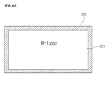
- FIGS. 3a to 3f are cross-sectional views for illustrating the method for manufacturing a back electrode-type solar cell according to the first embodiment of the present disclosure.
- a first conductive crystalline silicon substrate 301 is prepared (S201), and a texturing process is performed to form unevenness 302 on the surface of the first conductive silicon substrate 301 (S202).
- the texturing process is performed to reduce light reflection at the surface of the substrate 301, and may be performed by wet etching or dry etching such as reactive ion etching.
- the unevenness structure of the surface may be formed at only the light-receiving surface, namely the front surface.
- the first conductive type may be p-type or n-type, and the second conductive type is opposite to the first conductive type. The following description will be based on that the first conductive type is n-type.
- a thermal diffusion control film 303 having a predetermined thickness is formed along a circumference of the substrate 301 (S203).
- the thermal diffusion control film 303 plays a role of controlling the degree of thermal diffusion at a certain region when a thermal diffusion process is performed, and the thickness should be set to allow ion implantation.
- the ion implantation includes all kinds of methods where ions are implanted in a particle state. Particularly, any one of ion implantation, ion doping, plasma doping and plasma ion showering may be used.
- a thermal diffusion control film 303 on the front surface of the substrate 301 may have a smaller thickness than that of the back surface and the side surfaces of the substrate so that p+ or n+ impurities may be diffused to the front surface of the substrate 301.
- the thermal diffusion control film 303 may be configured with, for example, a silicon oxide film (SiO 2 ) or a silicon oxide glass (SOG), and may be formed by a general film laminating method such as plasma enhanced chemical vapor deposition (PECVD), thermal oxidation, wet oxidation, spin-on method, spraying and sputtering.
- PECVD plasma enhanced chemical vapor deposition
- second conductive impurity ions namely p-type impurity ions such as boron (B) or the like, are implanted onto the back surface of the substrate 301 to form a p-type impurity region 304 (S204).
- the ions should pass through the thermal diffusion control film 303 and be implanted to a certain region of the back surface of the substrate 301, and this may be controlled by means of ion implantation energy, which is about 10 to 50 keV.
- the p-type impurity ions may be implanted by using any one of ion implanting, ion doping and plasma doping.
- the p-type impurity region 304 is activated by a thermal diffusion process described later.
- ions with a concentration corresponding thereto should be injected so that the p+ emitter region 307 may have a sheet resistance of 10 to 60 ⁇ /sq., and the p+ emitter region 307 may have a depth of about 0.3 to 2 ⁇ m.
- the thermal diffusion control film 303 and the substrate at the back surface of the substrate 301 are selectively removed at a portion corresponding to a region where the high-concentration back field layer (n+) 305 is formed (S205).
- the substrate is partially removed along with the thermal diffusion control film in order to remove the p-type impurity region so that the influence of the p-type impurity region to the concentration of the high-concentration back field layer (n+) generated by a thermal diffusion process described later may be minimized.
- the thermal diffusion control film 303 and a predetermined thickness of the substrate may be removed by irradiating laser onto the thermal diffusion control film 303 at a region where the high-concentration back field layer (n+) 305 is formed.
- the thickness of the substrate 301 removed by laser irradiation suitably corresponds to the depth of the p-type impurity region 304.
- an etching paste may be used instead of laser ablation.
- the thermal diffusion control film 303 and the predetermined thickness of the substrate 301 may be removed by applying an etching paste onto the thermal diffusion control film 303 by means of ink-jet printing or screen printing at a region where the high-concentration back field layer (n+) is formed.
- dry etching such as reactive ion etching may be used.
- the predetermined thickness of the substrate may be secondarily etched and removed by using an alkali solution or the like, and along with it, the substrate damaged when removing the thermal diffusion control film may be cured.
- a thermal diffusion process is performed to form the high-concentration back field layer (n+) 305 and the low-concentration front field layer (n-) 306 simultaneously and the p-type impurity region 304 is activated to form the p+ emitter region 307 (S206).
- the silicon substrate 301 is provided in a chamber, and first conductive impurity ions, namely gas (for example, POCl 3 ) containing n-type impurity ions, is supplied into the chamber so that phosphorus (P) ions are diffused into the substrate 301.
- the exposed region of the back surface of the substrate 301 by removing the thermal diffusion control film 303 exhibits relatively greater diffusion of impurity ions in comparison to a region where the thermal diffusion control film 303 is provided. Accordingly, the high-concentration back field layer (n+) 305 is formed at the exposed region of the back surface of the substrate 301, and the low-concentration front field layer (n-) 306 is formed at the front surface of the substrate 301 where the thermal diffusion control film 303 is provided.
- the high-concentration back field layer (n+) 305 and the low-concentration front field layer (n-) 306 may adjust concentrations of the impurity ions to have sheet resistances of 10 to 80 ⁇ /sq. and 50 to 150 ⁇ /sq respectively.
- the high-concentration back field layer (n+) 305 and the low-concentration front field layer (n-) 306 may have depths of 0.2 to 1.5 ⁇ m and 0.1 to 0.4 ⁇ m, respectively.
- BBr 3 gas may be used instead of the POCl 3 gas.
- the thermal diffusion process of the n-type impurity ions may use a method where a film is formed on the surface of the silicon substrate 301 by immersing the silicon substrate 301 in a solution containing n-type impurity ions, for example a phosphorous acid (H 3 PO 4 ) solution or a material containing phosphorus (P) or by applying the solution by means of spraying or performing spin-on coating or the like, followed by thermal treatment so that the phosphorus (P) ions are diffused into the substrate 301 to form the high-concentration back field layer (n+) 305 and the low-concentration front field layer (n-) 306.
- a solution containing n-type impurity ions for example a phosphorous acid (H 3 PO 4 ) solution or a material containing phosphorus (P)
- thermal treatment so that the phosphorus (P) ions are diffused into the substrate 301 to form the high-concentration back field layer (n+) 305 and the low-concentration front field layer
- FIGS. 4a to 4g are cross-sectional views for illustrating the method for manufacturing a back electrode-type solar cell according to the second embodiment of the present disclosure.
- the second embodiment of the present disclosure is characterized in that the diffusion of n-type impurity ions into the p+ emitter region 307 is perfectly prevented when the thermal diffusion process is performed.
- FIG. 4d in a state where the p-type impurity region 304 is formed, an anti-diffusion film 401 is laminated on the thermal diffusion control film 303 at the back surface of the substrate 301, and then, as shown in FIG. 4e , the thermal diffusion control film 303, the anti-diffusion film 401 and a predetermined thickness of the substrate are selectively removed at a portion where the high-concentration back field layer (n+) 305 is to be formed, to expose the back surface of the substrate 301.
- n+ high-concentration back field layer
- the anti-diffusion film 401 is representatively a film having an insulating film corresponding to the above, for example a silicon nitride film (SiNx), silicon oxide glass (SOG), an intrinsic amorphous silicon film or the like.
- SiNx silicon nitride film
- SOG silicon oxide glass
- the texturing process, the process of forming the thermal diffusion control film 303, and the process of forming the p electrode 308 and the n electrode 309 are identical to those of the first embodiment and not described in detail here.
- a back surface field may be easily formed by a single ion implantation process and a single thermal diffusion process, and the patterning work may be minimized.
Landscapes
- Photovoltaic Devices (AREA)
Abstract
Description
- The present disclosure relates to a method for manufacturing a back electrode-type solar cell, and more particularly, to a method for manufacturing a back electrode-type solar cell, which may minimize the number of processes by grafting a doping process using ion implantation and a thermal diffusion process when forming a p+ region and an n+ region at the back surface of a substrate.
- A solar cell is a core element of solar-light power generation, which directly transforms solar light into electricity, and it may be basically considered as a diode having a p-n junction. Solar light is transformed into electricity by a solar cell as follows. If solar light is incident to a p-n junction of a solar cell, an electron-hole pair is generated, and due to the electric field, electrons move to an n layer and holes move to a p layer, thereby generating photoelectromotive force between the p-n junctions. In this way, if a load or system is connected to both terminals of the solar cell, an electric power may flow to generate power.
- A general solar cell is configured to have a front surface and a back electrode respectively at front and back surfaces of the solar cell. Since the front electrode is provided to the front surface which is a light-receiving surface, the light-receiving area decreases as much as the area of the front electrode. In order to solve the decrease of the light-receiving area, a back electrode-type solar cell has been proposed. The back electrode-type solar cell maximizes the light-receiving area of the front surface of the solar cell by providing a (+) electrode and a (-) electrode on a back surface of the solar cell.
-
FIG. 1 is a cross-sectional view showing a back electrode-type solar cell proposed inUS 7,339,110 . Referring toFIG. 1 , a p+ region where p-type impurity ions are implanted and a n+ region where n-type impurity ions are implanted by thermal diffusion are provided at the back surface of a silicon substrate, and interdigitatedmetal electrodes - In a method for manufacturing a back electrode-type solar cell disclosed in
US 7,339,110 , thermal diffusion processes are respectively performed to form a p+ region and an n+ region, and an oxide film generated by each thermal diffusion process should be removed. When the thermal diffusion process is performed to form the n+ region, in order to define the n+ region, a process of selectively patterning an oxide film generated when the p+ region is formed is added. - As described above, in the conventional method for manufacturing a back electrode-type solar cell, two thermal diffusion processes must be performed, and at least four photolithography processes and etching processes are required for patterning oxide films and etching masks, resulting in very complicated processes.
- The present disclosure is designed to solve the above problem and the present disclosure is directed to providing a method for manufacturing a back electrode-type solar cell, which may minimize the number of processes by grafting a doping process using ion implantation and a thermal diffusion process when forming a p+ region and an n+ region at the back surface of a substrate.
- In one general aspect, the present disclosure provides a method for manufacturing a back electrode-type solar cell, which includes: preparing an n-type crystalline silicon substrate; forming a thermal diffusion control film on a front surface, a back surface and a side surface of the substrate; forming a p-type impurity region by implanting p-type impurity ions onto the back surface of the substrate; patterning the thermal diffusion control film so that the back surface of the substrate is selectively exposed; and forming a high-concentration back field layer (n+) at an exposed region of the back surface of the substrate and a low-concentration front field layer (n-) at the front surface of the substrate by performing a thermal diffusion process, and activating the p-type impurity region to form a p+ emitter region.
- In the patterning of the thermal diffusion control film so that the back surface of the substrate is selectively exposed, the thermal diffusion control film and a predetermined depth of the substrate may be removed at a region where the high-concentration back field layer (n+) is to be formed. In addition, when the thermal diffusion control film and the predetermined depth of the substrate are removed at a region where the high-concentration back field layer (n+) is to be formed, laser may be irradiated onto the thermal diffusion control film at a region where the high-concentration back field layer (n+) is to be formed so that the thermal diffusion control film and the predetermined depth of the substrate are removed, an etching paste may be applied onto the thermal diffusion control film at a region where the high-concentration back field layer (n+) is to be formed so that the thermal diffusion control film and the predetermined depth of the substrate are removed, or the thermal diffusion control film and the predetermined depth of the substrate may be removed by means of reactive ion etching at a region where the high-concentration back field layer (n+) is to be formed. The thickness of the removed substrate may correspond to a depth of the p-type impurity region.
- In another general aspect, the present disclosure provides a method for manufacturing a back electrode-type solar cell, which includes: preparing an n-type crystalline silicon substrate; forming a thermal diffusion control film on a front surface, a back surface and a side surface of the substrate; forming a p-type impurity region by implanting p-type impurity ions onto the back surface of the substrate; forming an anti-diffusion film on the back surface of the substrate; patterning the thermal diffusion control film and the anti-diffusion film so that the back surface of the substrate is selectively exposed; and forming a high-concentration back field layer (n+) at an exposed region of the back surface of the substrate and a low-concentration front field layer (n-) at the front surface of the substrate by performing a thermal diffusion process, and activating the p-type impurity region to form a p+ emitter region.
- The thickness of the thermal diffusion control film formed at the front surface of the substrate may be relatively smaller than that of the thermal diffusion control films formed at the back surface and the side surface of the substrate. The p+ emitter region may have a sheet resistance of 10 to 60 Ω/sq., the high-concentration back field layer (n+) may have a sheet resistance of 10 to 80 Ω/sq., and the low-concentration front field layer (n-) may have a sheet resistance of 50 to 150 Ω/sq.
- The method for manufacturing a back electrode-type solar cell according to the present disclosure gives the following effects.
- A back surface field may be easily formed by a single ion implantation process and a single thermal diffusion process, and the patterning work may be minimized.
- The above and other objects, features and advantages of the present disclosure will become apparent from the following description of certain exemplary embodiments given in conjunction with the accompanying drawings, in which:
-
FIG. 1 is a diagram showing a conventional back electrode-type solar cell; -
FIG. 2 is a flowchart for illustrating a method for manufacturing a back electrode-type solar cell according to a first embodiment of the present disclosure; -
FIGS. 3a to 3f are cross-sectional views for illustrating the method for manufacturing a back electrode-type solar cell according to the first embodiment of the present disclosure; and -
FIGS. 4a to 4g are cross-sectional views for illustrating the method for manufacturing a back electrode-type solar cell according to a second embodiment of the present disclosure. - Hereinafter, a method for manufacturing a back electrode-type solar cell according to an embodiment of the present disclosure will be described in detail with reference to the accompanying drawings.
FIG. 2 is a flowchart for illustrating a method for manufacturing a back electrode-type solar cell according to a first embodiment of the present disclosure, andFIGS. 3a to 3f are cross-sectional views for illustrating the method for manufacturing a back electrode-type solar cell according to the first embodiment of the present disclosure. - First, as shown in
FIGS. 2 and3a , a first conductivecrystalline silicon substrate 301 is prepared (S201), and a texturing process is performed to formunevenness 302 on the surface of the first conductive silicon substrate 301 (S202). The texturing process is performed to reduce light reflection at the surface of thesubstrate 301, and may be performed by wet etching or dry etching such as reactive ion etching. The unevenness structure of the surface may be formed at only the light-receiving surface, namely the front surface. The first conductive type may be p-type or n-type, and the second conductive type is opposite to the first conductive type. The following description will be based on that the first conductive type is n-type. - In a state where the texturing process is completed, as shown in
FIG. 3b , a thermaldiffusion control film 303 having a predetermined thickness is formed along a circumference of the substrate 301 (S203). The thermaldiffusion control film 303 plays a role of controlling the degree of thermal diffusion at a certain region when a thermal diffusion process is performed, and the thickness should be set to allow ion implantation. When impurity ions explained later are implanted, the ion implantation includes all kinds of methods where ions are implanted in a particle state. Particularly, any one of ion implantation, ion doping, plasma doping and plasma ion showering may be used. - In addition, when a thermal diffusion process is performed, a thermal
diffusion control film 303 on the front surface of thesubstrate 301 may have a smaller thickness than that of the back surface and the side surfaces of the substrate so that p+ or n+ impurities may be diffused to the front surface of thesubstrate 301. The thermaldiffusion control film 303 may be configured with, for example, a silicon oxide film (SiO2) or a silicon oxide glass (SOG), and may be formed by a general film laminating method such as plasma enhanced chemical vapor deposition (PECVD), thermal oxidation, wet oxidation, spin-on method, spraying and sputtering. - In a state where the thermal
diffusion control film 303 is laminated on the front surface, the back surface and the side surface of thesubstrate 301, as shown inFIG. 3c , second conductive impurity ions, namely p-type impurity ions such as boron (B) or the like, are implanted onto the back surface of thesubstrate 301 to form a p-type impurity region 304 (S204). The ions should pass through the thermaldiffusion control film 303 and be implanted to a certain region of the back surface of thesubstrate 301, and this may be controlled by means of ion implantation energy, which is about 10 to 50 keV. Along with it, the p-type impurity ions may be implanted by using any one of ion implanting, ion doping and plasma doping. - In addition, the p-
type impurity region 304 is activated by a thermal diffusion process described later. When the p-type impurity region 304 is formed, ions with a concentration corresponding thereto should be injected so that thep+ emitter region 307 may have a sheet resistance of 10 to 60 Ω/sq., and thep+ emitter region 307 may have a depth of about 0.3 to 2 µm. - In a state where the
p+ emitter region 307 is formed, as shown inFIG. 3d , the thermaldiffusion control film 303 and the substrate at the back surface of thesubstrate 301 are selectively removed at a portion corresponding to a region where the high-concentration back field layer (n+) 305 is formed (S205). The substrate is partially removed along with the thermal diffusion control film in order to remove the p-type impurity region so that the influence of the p-type impurity region to the concentration of the high-concentration back field layer (n+) generated by a thermal diffusion process described later may be minimized. - In order to selectively remove the thermal
diffusion control film 303 and a part of thesubstrate 301, laser ablation may be used. In other words, the thermaldiffusion control film 303 and a predetermined thickness of the substrate may be removed by irradiating laser onto the thermaldiffusion control film 303 at a region where the high-concentration back field layer (n+) 305 is formed. The thickness of thesubstrate 301 removed by laser irradiation suitably corresponds to the depth of the p-type impurity region 304. - In addition, an etching paste may be used instead of laser ablation. In detail, the thermal
diffusion control film 303 and the predetermined thickness of thesubstrate 301 may be removed by applying an etching paste onto the thermaldiffusion control film 303 by means of ink-jet printing or screen printing at a region where the high-concentration back field layer (n+) is formed. In addition to the above methods, dry etching such as reactive ion etching may be used. - When selectively removing the thermal
diffusion control film 303 and a part of thesubstrate 301, after the thermaldiffusion control film 303 is primarily removed, the predetermined thickness of the substrate may be secondarily etched and removed by using an alkali solution or the like, and along with it, the substrate damaged when removing the thermal diffusion control film may be cured. - In this state, as shown in
FIG. 3e , a thermal diffusion process is performed to form the high-concentration back field layer (n+) 305 and the low-concentration front field layer (n-) 306 simultaneously and the p-type impurity region 304 is activated to form the p+ emitter region 307 (S206). In detail, thesilicon substrate 301 is provided in a chamber, and first conductive impurity ions, namely gas (for example, POCl3) containing n-type impurity ions, is supplied into the chamber so that phosphorus (P) ions are diffused into thesubstrate 301. The exposed region of the back surface of thesubstrate 301 by removing the thermaldiffusion control film 303 exhibits relatively greater diffusion of impurity ions in comparison to a region where the thermaldiffusion control film 303 is provided. Accordingly, the high-concentration back field layer (n+) 305 is formed at the exposed region of the back surface of thesubstrate 301, and the low-concentration front field layer (n-) 306 is formed at the front surface of thesubstrate 301 where the thermaldiffusion control film 303 is provided. The high-concentration back field layer (n+) 305 and the low-concentration front field layer (n-) 306 may adjust concentrations of the impurity ions to have sheet resistances of 10 to 80 Ω/sq. and 50 to 150 Ω/sq respectively. Along with it, the high-concentration back field layer (n+) 305 and the low-concentration front field layer (n-) 306 may have depths of 0.2 to 1.5 µm and 0.1 to 0.4 µm, respectively. In a case where the first conductive impurity ions are p-type, BBr3 gas may be used instead of the POCl3 gas. - In addition to the above method using gas, the thermal diffusion process of the n-type impurity ions may use a method where a film is formed on the surface of the
silicon substrate 301 by immersing thesilicon substrate 301 in a solution containing n-type impurity ions, for example a phosphorous acid (H3PO4) solution or a material containing phosphorus (P) or by applying the solution by means of spraying or performing spin-on coating or the like, followed by thermal treatment so that the phosphorus (P) ions are diffused into thesubstrate 301 to form the high-concentration back field layer (n+) 305 and the low-concentration front field layer (n-) 306. - Subsequently, as shown in
FIG. 3f , if the thermaldiffusion control film 303 and a PSG film which is a byproduct of the thermal diffusion process are removed, the method for manufacturing a back electrode-type solar cell according to an embodiment of the present disclosure is completed. - Next, a method for manufacturing a back electrode-type solar cell according to a second embodiment of the present disclosure will be described.
FIGS. 4a to 4g are cross-sectional views for illustrating the method for manufacturing a back electrode-type solar cell according to the second embodiment of the present disclosure. - The second embodiment of the present disclosure is characterized in that the diffusion of n-type impurity ions into the
p+ emitter region 307 is perfectly prevented when the thermal diffusion process is performed. For this, as shown inFIG. 4d , in a state where the p-type impurity region 304 is formed, ananti-diffusion film 401 is laminated on the thermaldiffusion control film 303 at the back surface of thesubstrate 301, and then, as shown inFIG. 4e , the thermaldiffusion control film 303, theanti-diffusion film 401 and a predetermined thickness of the substrate are selectively removed at a portion where the high-concentration back field layer (n+) 305 is to be formed, to expose the back surface of thesubstrate 301. In this state, as shown inFIG. 4f , a thermal diffusion process is performed to form the high-concentration back field layer (n+) 305 and the low-concentration front field layer (n-) 306, and the p-type impurity region 304 is activated. Theanti-diffusion film 401 is representatively a film having an insulating film corresponding to the above, for example a silicon nitride film (SiNx), silicon oxide glass (SOG), an intrinsic amorphous silicon film or the like. Meanwhile, the texturing process, the process of forming the thermaldiffusion control film 303, and the process of forming the p electrode 308 and the n electrode 309 are identical to those of the first embodiment and not described in detail here. - According to the present disclosure, a back surface field may be easily formed by a single ion implantation process and a single thermal diffusion process, and the patterning work may be minimized.
- While the exemplary embodiments have been shown and described, it will be understood by those skilled in the art that various changes in form and details may be made thereto without departing from the spirit and scope of the present disclosure as defined by the appended claims.
Claims (15)
- A method for manufacturing a back electrode-type solar cell, comprising:preparing an n-type crystalline silicon substrate;forming a thermal diffusion control film on a front surface, a back surface and a side surface of the substrate;forming a p-type impurity region by implanting p-type impurity ions onto the back surface of the substrate;patterning the thermal diffusion control film so that the back surface of the substrate is selectively exposed; andforming a high-concentration back field layer (n+) at an exposed region of the back surface of the substrate and a low-concentration front field layer (n-) at the front surface of the substrate by performing a thermal diffusion process, and forming a p+ emitter region by activating the p-type impurity region.
- The method for manufacturing a back electrode-type solar cell according to claim 1, wherein, in said patterning of the thermal diffusion control film so that the back surface of the substrate is selectively exposed, comprising removing the thermal diffusion control film and a predetermined depth of the substrate at a region where the high-concentration back field layer (n+) is to be formed.
- The method for manufacturing a back electrode-type solar cell according to claim 2, wherein, in said removing of the thermal diffusion control film and a predetermined depth of the substrate at a region where the high-concentration back field layer (n+) is to be formed, comprising irradiating laser onto the thermal diffusion control film at a region where the high-concentration back field layer (n+) is to be formed.
- The method for manufacturing a back electrode-type solar cell according to claim 2, wherein, in said removing of the thermal diffusion control film and a predetermined depth of the substrate at a region where the high-concentration back field layer (n+) is to be formed, comprising applying an etching paste onto the thermal diffusion control film at a region where the high-concentration back field layer (n+) is to be formed.
- The method for manufacturing a back electrode-type solar cell according to claim 2, wherein, in said removing of the thermal diffusion control film and a predetermined depth of the substrate at a region where the high-concentration back field layer (n+) is to be formed, comprising removing the thermal diffusion control film and the predetermined depth of the substrate at a region where the high-concentration back field layer (n+) is to be formed by means of reactive ion etching.
- The method for manufacturing a back electrode-type solar cell according to claim 2, wherein the thickness of the removed substrate corresponds to a depth of the p-type impurity region.
- A method for manufacturing a back electrode-type solar cell, comprising:preparing an n-type crystalline silicon substrate;forming a thermal diffusion control film on a front surface, a back surface and a side surface of the substrate;forming a p-type impurity region by implanting p-type impurity ions onto the back surface of the substrate;forming an anti-diffusion film on the back surface of the substrate;patterning the thermal diffusion control film and the anti-diffusion film so that the back surface of the substrate is selectively exposed; andforming a high-concentration back field layer (n+) at an exposed region of the back surface of the substrate and a low-concentration front field layer (n-) at the front surface of the substrate by performing a thermal diffusion process, and forming a p+ emitter region by activating the p-type impurity region.
- The method for manufacturing a back electrode-type solar cell according to claim 7, wherein, in said patterning of the thermal diffusion control film and the anti-diffusion film so that the back surface of the substrate is selectively exposed, comprising removing the thermal diffusion control film, the anti-diffusion film and a predetermined depth of the substrate at a region where the high-concentration back field layer (n+) is to be formed.
- The method for manufacturing a back electrode-type solar cell according to claim 8, wherein, when the thermal diffusion control film, the anti-diffusion film and the predetermined depth of the substrate are removed at a region where the high-concentration back field layer (n+) is to be formed, comprising irradiating laser onto the thermal diffusion control film at a region where the high-concentration back field layer (n+) is to be formed.
- The method for manufacturing a back electrode-type solar cell according to claim 8, wherein, when the thermal diffusion control film, the anti-diffusion film and the predetermined depth of the substrate are removed at a region where the high-concentration back field layer (n+) is to be formed, comprising removing the thermal diffusion control film and the predetermined depth of the substrate at a region where the high-concentration back field layer (n+) is to be formed by means of reactive ion etching.
- The method for manufacturing a back electrode-type solar cell according to claim 8, wherein the thickness of the removed substrate corresponds to a depth of the p-type impurity region.
- The method for manufacturing a back electrode-type solar cell according to claim 1 or 7, wherein the thickness of the thermal diffusion control film formed at the front surface of the substrate is relatively smaller than that of the thermal diffusion control films formed at the back surface and the side surface of the substrate.
- The method for manufacturing a back electrode-type solar cell according to claim 1 or 7, wherein the p+ emitter region has a sheet resistance of 10 to 60 Ω/sq.
- The method for manufacturing a back electrode-type solar cell according to claim 1 or 7, wherein the high-concentration back field layer (n+) has a sheet resistance of 10 to 80 Ω/sq.
- The method for manufacturing a back electrode-type solar cell according to claim 1 or 2, wherein the low-concentration front field layer (n-) has a sheet resistance of 50 to 150 Ω/sq.
Applications Claiming Priority (2)
| Application Number | Priority Date | Filing Date | Title |
|---|---|---|---|
| KR1020100004272A KR101027829B1 (en) | 2010-01-18 | 2010-01-18 | Manufacturing method of back electrode solar cell |
| PCT/KR2011/000354 WO2011087341A2 (en) | 2010-01-18 | 2011-01-18 | Method for fabricating a back contact solar cell |
Publications (2)
| Publication Number | Publication Date |
|---|---|
| EP2528105A2 true EP2528105A2 (en) | 2012-11-28 |
| EP2528105A4 EP2528105A4 (en) | 2015-08-19 |
Family
ID=44049808
Family Applications (1)
| Application Number | Title | Priority Date | Filing Date |
|---|---|---|---|
| EP11733128.0A Withdrawn EP2528105A4 (en) | 2010-01-18 | 2011-01-18 | METHOD FOR MANUFACTURING REAR CONTACT SOLAR CELL |
Country Status (6)
| Country | Link |
|---|---|
| US (1) | US8461011B2 (en) |
| EP (1) | EP2528105A4 (en) |
| JP (1) | JP5518212B2 (en) |
| KR (1) | KR101027829B1 (en) |
| CN (1) | CN102725867B (en) |
| WO (1) | WO2011087341A2 (en) |
Cited By (4)
| Publication number | Priority date | Publication date | Assignee | Title |
|---|---|---|---|---|
| CN103311376A (en) * | 2013-06-26 | 2013-09-18 | 英利集团有限公司 | Manufacturing method for N type solar cell |
| WO2015044342A1 (en) * | 2013-09-27 | 2015-04-02 | International Solar Energy Research Center Konstanz E.V. | Method for producing a solar cell |
| CN104810363A (en) * | 2014-01-26 | 2015-07-29 | 北大方正集团有限公司 | Power integrated device and manufacture method thereof |
| EP3116035A1 (en) * | 2015-07-07 | 2017-01-11 | Lg Electronics Inc. | Solar cell and method of manufacturing the same |
Families Citing this family (23)
| Publication number | Priority date | Publication date | Assignee | Title |
|---|---|---|---|---|
| JP5723143B2 (en) * | 2010-12-06 | 2015-05-27 | シャープ株式会社 | Manufacturing method of back electrode type solar cell and back electrode type solar cell |
| CN102832263B (en) * | 2011-06-15 | 2015-01-14 | 茂迪股份有限公司 | Solar cell with back electric field structure and manufacturing method thereof |
| KR20130062775A (en) * | 2011-12-05 | 2013-06-13 | 엘지전자 주식회사 | Solar cell and method for manufacturing the same |
| KR101875747B1 (en) * | 2011-12-16 | 2018-07-06 | 엘지전자 주식회사 | Method for manufacturing solar cell |
| KR101958819B1 (en) * | 2012-01-27 | 2019-03-15 | 엘지전자 주식회사 | Method for manufacturing a bifacial solar cell |
| KR101345506B1 (en) * | 2012-02-01 | 2013-12-27 | 현대중공업 주식회사 | Back contact solar cell and method for fabricating the same |
| KR101872786B1 (en) * | 2012-06-22 | 2018-06-29 | 엘지전자 주식회사 | Method for manufacturing solar cell and dopant layer thereof |
| US8901010B2 (en) * | 2013-03-15 | 2014-12-02 | Sunpower Corporation | Methods for improving solar cell lifetime and efficiency |
| CN103367539B (en) * | 2013-06-26 | 2015-09-09 | 英利集团有限公司 | Manufacturing method of IBC solar cell and IBC solar cell |
| CN103560168A (en) * | 2013-10-23 | 2014-02-05 | 中电电气(扬州)光伏有限公司 | Process for manufacturing PERC solar cell |
| JP2015144149A (en) * | 2014-01-31 | 2015-08-06 | シャープ株式会社 | Photoelectric conversion device and method for manufacturing photoelectric conversion device |
| US20150349180A1 (en) * | 2014-05-30 | 2015-12-03 | David D. Smith | Relative dopant concentration levels in solar cells |
| KR101661807B1 (en) * | 2014-07-28 | 2016-09-30 | 엘지전자 주식회사 | Solar cell and the manufacturing mathod thereof |
| DE102014215893A1 (en) * | 2014-08-11 | 2016-02-11 | Fraunhofer-Gesellschaft zur Förderung der angewandten Forschung e.V. | Method for generating doping regions in a semiconductor layer of a semiconductor component |
| CN105702797A (en) * | 2014-11-27 | 2016-06-22 | 上海晶玺电子科技有限公司 | Manufacturing method of double-face battery |
| KR102320551B1 (en) * | 2015-01-16 | 2021-11-01 | 엘지전자 주식회사 | Method for manufacturing solar cell |
| US20160284913A1 (en) * | 2015-03-27 | 2016-09-29 | Staffan WESTERBERG | Solar cell emitter region fabrication using substrate-level ion implantation |
| CN104752567A (en) * | 2015-04-24 | 2015-07-01 | 中建材浚鑫科技股份有限公司 | Cooling junction pushing and diffusion process |
| US9634178B1 (en) * | 2015-12-16 | 2017-04-25 | Sunpower Corporation | Method of using laser welding to ohmic contact of metallic thermal and diffusion barrier layer for foil-based metallization of solar cells |
| KR102657230B1 (en) * | 2016-11-04 | 2024-04-12 | 오씨아이 주식회사 | Solar cell and manufacturing method thereof |
| CN113871494B (en) * | 2020-06-30 | 2024-03-15 | 泰州隆基乐叶光伏科技有限公司 | Solar cell and manufacturing method thereof |
| CN116525697A (en) * | 2023-04-28 | 2023-08-01 | 正泰新能科技有限公司 | Back contact type solar cell and preparation method thereof |
| CN118867057B (en) * | 2024-09-24 | 2024-12-20 | 玉环晶科能源有限公司 | Solar cell and method for manufacturing the same |
Family Cites Families (12)
| Publication number | Priority date | Publication date | Assignee | Title |
|---|---|---|---|---|
| JP3530026B2 (en) * | 1997-06-30 | 2004-05-24 | 株式会社東芝 | Semiconductor device and manufacturing method thereof |
| KR100366353B1 (en) * | 2000-12-20 | 2002-12-31 | 삼성에스디아이 주식회사 | Formation method of junction for solar cell |
| US7339110B1 (en) | 2003-04-10 | 2008-03-04 | Sunpower Corporation | Solar cell and method of manufacture |
| KR100766254B1 (en) | 2005-10-20 | 2007-10-15 | 동부일렉트로닉스 주식회사 | Method of forming bonding layer for solar cell |
| CN106409970A (en) * | 2005-12-21 | 2017-02-15 | 太阳能公司 | Back side contact solar cell structures and fabrication processes |
| DE102006003283A1 (en) * | 2006-01-23 | 2007-07-26 | Gp Solar Gmbh | Fabricating method for semiconductor component e.g. solar cell, involves forming diffusion-inhibiting layer, partial removal of layer in highly doped region, formation of dopant source and diffusion of dopant from dopant source |
| KR100757797B1 (en) | 2006-02-03 | 2007-09-11 | 주식회사 실트론 | Method for manufacturing back electrode of single crystal solar cell |
| GB2442254A (en) * | 2006-09-29 | 2008-04-02 | Renewable Energy Corp Asa | Back contacted solar cell |
| JP2008186927A (en) * | 2007-01-29 | 2008-08-14 | Sharp Corp | Back junction solar cell and manufacturing method thereof |
| DE102008013445A1 (en) * | 2008-02-15 | 2009-08-27 | Ersol Solar Energy Ag | Process for producing monocrystalline silicon solar cells with rear-side emitter and base contacts and solar cell, produced by such a process |
| DE102008013446A1 (en) * | 2008-02-15 | 2009-08-27 | Ersol Solar Energy Ag | Process for producing monocrystalline n-silicon solar cells and solar cell, produced by such a process |
| US20090227095A1 (en) * | 2008-03-05 | 2009-09-10 | Nicholas Bateman | Counterdoping for solar cells |
-
2010
- 2010-01-18 KR KR1020100004272A patent/KR101027829B1/en not_active Expired - Fee Related
-
2011
- 2011-01-18 US US13/519,249 patent/US8461011B2/en not_active Expired - Fee Related
- 2011-01-18 JP JP2012547035A patent/JP5518212B2/en not_active Expired - Fee Related
- 2011-01-18 EP EP11733128.0A patent/EP2528105A4/en not_active Withdrawn
- 2011-01-18 WO PCT/KR2011/000354 patent/WO2011087341A2/en not_active Ceased
- 2011-01-18 CN CN201180007151.4A patent/CN102725867B/en not_active Expired - Fee Related
Cited By (6)
| Publication number | Priority date | Publication date | Assignee | Title |
|---|---|---|---|---|
| CN103311376A (en) * | 2013-06-26 | 2013-09-18 | 英利集团有限公司 | Manufacturing method for N type solar cell |
| WO2015044342A1 (en) * | 2013-09-27 | 2015-04-02 | International Solar Energy Research Center Konstanz E.V. | Method for producing a solar cell |
| CN104810363A (en) * | 2014-01-26 | 2015-07-29 | 北大方正集团有限公司 | Power integrated device and manufacture method thereof |
| CN104810363B (en) * | 2014-01-26 | 2018-04-17 | 北大方正集团有限公司 | Power IC device and preparation method thereof |
| EP3116035A1 (en) * | 2015-07-07 | 2017-01-11 | Lg Electronics Inc. | Solar cell and method of manufacturing the same |
| EP3419059A1 (en) * | 2015-07-07 | 2018-12-26 | LG Electronics Inc. | Method of manufacturing a solar cell |
Also Published As
| Publication number | Publication date |
|---|---|
| KR101027829B1 (en) | 2011-04-07 |
| JP5518212B2 (en) | 2014-06-11 |
| US8461011B2 (en) | 2013-06-11 |
| CN102725867A (en) | 2012-10-10 |
| JP2013516082A (en) | 2013-05-09 |
| EP2528105A4 (en) | 2015-08-19 |
| WO2011087341A3 (en) | 2011-12-08 |
| CN102725867B (en) | 2015-03-25 |
| US20120282732A1 (en) | 2012-11-08 |
| WO2011087341A2 (en) | 2011-07-21 |
Similar Documents
| Publication | Publication Date | Title |
|---|---|---|
| US8461011B2 (en) | Method for fabricating a back contact solar cell | |
| JP6831964B2 (en) | Solar cell | |
| EP2702614B1 (en) | Method of forming emitters for a back-contact solar cell | |
| US9087956B2 (en) | Solar cell and fabrication method thereof | |
| US8481356B2 (en) | Method for manufacturing a back contact solar cell | |
| KR101225978B1 (en) | Sollar Cell And Fabrication Method Thereof | |
| CN101933156A (en) | Solar cell and method of manufacturing same | |
| TWI353065B (en) | Method for manufacturing solar cell and solar cell | |
| US20130048069A1 (en) | Solar Cell Having Selective Emitter | |
| JP2017504950A (en) | Solar cell emitter region fabrication using ion implantation. | |
| KR101360658B1 (en) | Method for forming selective emitter in a solar cell | |
| KR101125450B1 (en) | Method for fabricating back contact solar cell | |
| KR101089992B1 (en) | Selective Emitter Formation Method of Solar Cell | |
| KR20110020062A (en) | Manufacturing method of back junction solar cell using plasma doping and diffusion and solar cell | |
| US20120255608A1 (en) | Back-surface-field type of heterojunction solar cell and a production method therefor | |
| KR20110078549A (en) | Selective Emitter Formation Method of Solar Cell | |
| US20120295391A1 (en) | Method of manufacturing a solar cell | |
| KR20150021829A (en) | Method for fabricating solar cell | |
| KR101612132B1 (en) | Method for fabricating back contact solar cell | |
| KR20130048939A (en) | Method for forming selective emitter in a solar cell | |
| KR20140026670A (en) | Back contact solar cell and method of fabricating the same | |
| HK1188337A (en) | Manufacturing method of bifacial solar cells | |
| KR20120094215A (en) | Method for forming selective emitter in a solar cell | |
| KR20120003613A (en) | Manufacturing method of back electrode solar cell |
Legal Events
| Date | Code | Title | Description |
|---|---|---|---|
| PUAI | Public reference made under article 153(3) epc to a published international application that has entered the european phase |
Free format text: ORIGINAL CODE: 0009012 |
|
| 17P | Request for examination filed |
Effective date: 20120629 |
|
| AK | Designated contracting states |
Kind code of ref document: A2 Designated state(s): AL AT BE BG CH CY CZ DE DK EE ES FI FR GB GR HR HU IE IS IT LI LT LU LV MC MK MT NL NO PL PT RO RS SE SI SK SM TR |
|
| DAX | Request for extension of the european patent (deleted) | ||
| A4 | Supplementary search report drawn up and despatched |
Effective date: 20150722 |
|
| RIC1 | Information provided on ipc code assigned before grant |
Ipc: H01L 31/042 20140101AFI20150713BHEP Ipc: H01L 31/18 20060101ALI20150713BHEP |
|
| STAA | Information on the status of an ep patent application or granted ep patent |
Free format text: STATUS: THE APPLICATION IS DEEMED TO BE WITHDRAWN |
|
| 18D | Application deemed to be withdrawn |
Effective date: 20160218 |