US8901010B2 - Methods for improving solar cell lifetime and efficiency - Google Patents
Methods for improving solar cell lifetime and efficiency Download PDFInfo
- Publication number
- US8901010B2 US8901010B2 US13/837,802 US201313837802A US8901010B2 US 8901010 B2 US8901010 B2 US 8901010B2 US 201313837802 A US201313837802 A US 201313837802A US 8901010 B2 US8901010 B2 US 8901010B2
- Authority
- US
- United States
- Prior art keywords
- solar cell
- front side
- receiving medium
- region
- lightly doped
- Prior art date
- Legal status (The legal status is an assumption and is not a legal conclusion. Google has not performed a legal analysis and makes no representation as to the accuracy of the status listed.)
- Active
Links
Images


Classifications
-
- H01L21/02288—
-
- H01L31/18—
-
- H—ELECTRICITY
- H10—SEMICONDUCTOR DEVICES; ELECTRIC SOLID-STATE DEVICES NOT OTHERWISE PROVIDED FOR
- H10F—INORGANIC SEMICONDUCTOR DEVICES SENSITIVE TO INFRARED RADIATION, LIGHT, ELECTROMAGNETIC RADIATION OF SHORTER WAVELENGTH OR CORPUSCULAR RADIATION
- H10F71/00—Manufacture or treatment of devices covered by this subclass
-
- H—ELECTRICITY
- H10—SEMICONDUCTOR DEVICES; ELECTRIC SOLID-STATE DEVICES NOT OTHERWISE PROVIDED FOR
- H10F—INORGANIC SEMICONDUCTOR DEVICES SENSITIVE TO INFRARED RADIATION, LIGHT, ELECTROMAGNETIC RADIATION OF SHORTER WAVELENGTH OR CORPUSCULAR RADIATION
- H10F77/00—Constructional details of devices covered by this subclass
- H10F77/20—Electrodes
- H10F77/206—Electrodes for devices having potential barriers
- H10F77/211—Electrodes for devices having potential barriers for photovoltaic cells
-
- H—ELECTRICITY
- H10—SEMICONDUCTOR DEVICES; ELECTRIC SOLID-STATE DEVICES NOT OTHERWISE PROVIDED FOR
- H10F—INORGANIC SEMICONDUCTOR DEVICES SENSITIVE TO INFRARED RADIATION, LIGHT, ELECTROMAGNETIC RADIATION OF SHORTER WAVELENGTH OR CORPUSCULAR RADIATION
- H10F77/00—Constructional details of devices covered by this subclass
- H10F77/30—Coatings
- H10F77/306—Coatings for devices having potential barriers
- H10F77/311—Coatings for devices having potential barriers for photovoltaic cells
-
- Y—GENERAL TAGGING OF NEW TECHNOLOGICAL DEVELOPMENTS; GENERAL TAGGING OF CROSS-SECTIONAL TECHNOLOGIES SPANNING OVER SEVERAL SECTIONS OF THE IPC; TECHNICAL SUBJECTS COVERED BY FORMER USPC CROSS-REFERENCE ART COLLECTIONS [XRACs] AND DIGESTS
- Y02—TECHNOLOGIES OR APPLICATIONS FOR MITIGATION OR ADAPTATION AGAINST CLIMATE CHANGE
- Y02E—REDUCTION OF GREENHOUSE GAS [GHG] EMISSIONS, RELATED TO ENERGY GENERATION, TRANSMISSION OR DISTRIBUTION
- Y02E10/00—Energy generation through renewable energy sources
- Y02E10/50—Photovoltaic [PV] energy
- Y02E10/547—Monocrystalline silicon PV cells
-
- Y—GENERAL TAGGING OF NEW TECHNOLOGICAL DEVELOPMENTS; GENERAL TAGGING OF CROSS-SECTIONAL TECHNOLOGIES SPANNING OVER SEVERAL SECTIONS OF THE IPC; TECHNICAL SUBJECTS COVERED BY FORMER USPC CROSS-REFERENCE ART COLLECTIONS [XRACs] AND DIGESTS
- Y02—TECHNOLOGIES OR APPLICATIONS FOR MITIGATION OR ADAPTATION AGAINST CLIMATE CHANGE
- Y02P—CLIMATE CHANGE MITIGATION TECHNOLOGIES IN THE PRODUCTION OR PROCESSING OF GOODS
- Y02P70/00—Climate change mitigation technologies in the production process for final industrial or consumer products
- Y02P70/50—Manufacturing or production processes characterised by the final manufactured product
Definitions
- Embodiments of the subject matter described herein relate generally to solar cell manufacture. More particularly, embodiments of the subject matter relate to depositing etch resists on solar cells and techniques for manufacture.
- Solar cells are well known devices for converting solar radiation to electrical energy. They can be fabricated on a semiconductor wafer using semiconductor processing technology.
- a solar cell includes P-type and N-type diffusion regions. Solar radiation impinging on the solar cell creates electrons and holes that migrate to the diffusion regions, thereby creating voltage differentials between the diffusion regions.
- both the diffusion regions and the metal contact fingers coupled to them are on the backside of the solar cell. The contact fingers allow an external electrical circuit to be coupled to and be powered by the solar cell.
- Lifetime is an important characteristic of a solar cell as it is directly related to the solar cell's capability to generate power. Accordingly, techniques for improving the fabrication process, reducing the cost of manufacturing and increasing the efficiency of solar cells are generally desirable.
- Such techniques include methods for fabricating solar cells, without damaging the solar cell structure, where one or more embodiments prevent damage to the solar cell and allow for improved solar cell lifetime and increased solar cell efficiency.
- a method for forming a first etch resist on a solar cell includes providing a solar cell having a front side which faces the sun during normal operation and a back side opposite the front side.
- the method includes placing the solar cell on a receiving medium with the front side of the solar cell placed on an upper surface of the receiving medium, where the solar cell includes a lightly doped diffusion region and a texturized region on the front side.
- the method includes depositing the first etch resist on the back side of the solar cell using a contact printing method and where the upper surface of the receiving medium prevents damage to the to the lightly doped diffusion region and damage to the texturized region on the front side of the solar cell during a printing process.
- the method also includes removing the solar cell from the receiving medium and curing the first etch resist.
- the first etch resist is a plating resist commonly used in the fabrication or manufacture of solar cells.
- forming the first etch resist includes screen printing the first etch resist.
- a non-contact printing method is used to prevent damage to the texturized region and lightly doped diffusion region during the printing process, such as ink-jet printing.
- a first protective layer can be deposited over the front side of the solar cell prior to depositing a first etch resist, where the first protective layer, instead of the receiving medium, protects the texturized region and lightly doped diffusion region from damage during printing.
- a method for transferring a solar cell from a first location to a second location includes providing a solar cell having a front side which faces the sun during normal operation and a back side opposite the front side and a silicon substrate, where the silicon substrate includes a texturized region and a lightly doped diffusion region on the front side of the solar cell.
- the method includes picking the solar cell from on a first location using a contact transfer tool, where a bottom surface of the contact transfer tool contacts the front side of the solar cell.
- the method also includes placing the solar cell on a second location, where the bottom surface of the contact transfer tool prevents damage to the texturized region and the lightly doped region during the pick-and-place operation.
- a non-contact transfer method is used to prevent damage to the texturized region and lightly doped diffusion region during the transfer process from the first location to a second location.
- a first protective layer is deposited over the front side of the solar cell prior to the transfer process, where the first protective layer, instead of the receiving medium, protects the texturized region and lightly doped diffusion region from damage during transfer.
- a method for manufacturing a solar cell includes providing a solar cell having a front side which faces the sun during normal operation, a back side opposite the front side and a silicon substrate.
- the method includes forming a doped region on a silicon substrate of the solar cell and etching a texturized region on the silicon substrate.
- a lightly doped diffusion region is formed on the silicon substrate, where the lightly doped diffusion region is formed on the same side as the texturized region.
- the method includes forming a first protective layer over the texturized region and lightly doped diffusion region, where the first protective layer prevents damage to the texturized region and lightly doped diffusion region during manufacturing.
- a dielectric layer is deposited over the texturized region, lightly doped diffusion region and the doped region.
- a plurality of contact openings are formed through the dielectric layer.
- the method also includes forming a first metal grid electrically coupled to the doped region through the contact openings and a second metal grid being electrically coupled to the first metal grid.
- the first protective layer is composed of an etch resist.
- a method for manufacturing a solar cell includes providing a solar cell having a front side which faces the sun during normal operation, a back side opposite the front side and a silicon substrate.
- the method includes forming a doped region on a silicon substrate of the solar cell and etching a texturized region on the silicon substrate.
- a lightly doped diffusion region is formed on the silicon substrate, where the lightly doped diffusion region is formed on the same side as the texturized region.
- the method includes depositing a first dielectric layer over the texturized region and lightly doped diffusion region, where the first dielectric layer prevents damage to the texturized region and lightly doped diffusion region during manufacturing.
- the method also includes depositing a second dielectric layer over the doped region.
- a plurality of contact openings are formed through the second dielectric layer. Furthermore, the method also includes forming a first metal grid electrically coupled to the doped region through the contact openings and a second metal grid being electrically coupled to the first metal grid.
- the first dielectric layer is composed of silicon nitride (SiN) with a thickness in the range of 100-3000 Angstroms on the front side of the solar cell.
- FIG. 1 is a cross-sectional representation of a solar cell undergoing a contact force
- FIG. 2 is a cross-sectional representation of a local high recombination area of the solar cell of FIG. 1 ;
- FIGS. 3-9 are a cross-sectional representations of a solar cell used in accordance with the presented methods of protecting a texturized region of a solar cell;
- FIG. 10 is a graphical representation of test results for solar cell lifetime comparison between several solar cells used in accordance with the presented methods of protecting a texturized region of a solar cell;
- FIG. 11 is a graphical representation of test results for solar cell efficiency comparison between several solar cells used in accordance with the presented methods of protecting a texturized region of a solar cell;
- FIGS. 12 and 13 are flowchart representations of the presented methods for forming a first etch resist on a solar cell
- FIGS. 14 and 15 are flowchart representations of the presented methods for transferring a solar cell from a first location to a second location.
- FIGS. 16 and 17 are flowchart representations of the presented methods of manufacturing a solar cell.
- the mode of damage can be from a solar cell fabrication process or a transfer method which can apply a contact force onto a solar cell.
- FIG. 1 shows a solar cell undergoing such a contact force.
- FIG. 1 illustrates a solar cell undergoing a contact force.
- the solar cell 100 can include a silicon substrate 110 having a texturized region 120 and a diffusion region 122 .
- screen printing is a common process used to form masks for subsequent etching, cleaning and in further preparation for metal contact formation. Screen printing requires the use of a squeegee to push an etch resist through a screen onto a solar cell to form a mask, where the squeegee pushes the solar cell 100 against a receiving medium 150 of a screen printer.
- the contact force 140 can be, but is not limited to, a force exerted by the squeegee on the solar cell during screen printing.
- uneven surfaces can have raised surfaces 156 and lowered surfaces 158 , where raised surfaces 156 can provide areas which concentrate a counter force 141 , due to the contact force 140 , on the texturized region 120 of the solar cell 100 .
- the counter forces 141 can in turn damage localized areas of the texturized region 120 and the doped region 122 , resulting in defects such as local high recombination areas 130 within the silicon substrate 110 of the solar cell 100 .
- the local high recombination areas 130 can eventually lead to lifetime failure and solar cell efficiency loss.
- FIG. 2 illustrates a cross-sectional representation of a local high recombination area of the solar cell of FIG. 1 .
- the local high recombination area 130 can include dislocations 132 , such as break points, within the diffusion region 122 of the silicon substrate 110 .
- the local high recombination area 130 can also include chips 134 along the edges of the texturized region 120 . Scraping can also occur between the texturized region 120 and the receiving medium 150 of FIG. 2 , allowing for contamination 136 on the solar cell 100 from foreign material scraped off the receiving medium 150 .
- screen printing can induce damage to the texturized region and diffusion region of a solar cell resulting in lifetime degradation and solar cell efficiency loss.
- other modes of damage are known, such as due to transferring of solar cells, where transferring can include any method, either automatic or manual, used to transfer solar cells from a first location to a second location during, prior, after and in-between solar cell fabrication or manufacturing processes.
- lateral damage, or scratching, to the texturized region can also occur when a solar cell is improperly secured on a receiving medium during transfer.
- too much pressure exerted from a vacuum pad or gripper securing a solar cell during transfer can also result in damage of the texturized region and doped region as discussed above.
- the receiving medium can have a number of different interpretations such as a chuck, palette, jig, walking beam, mount or conveyor, where the receiving medium is not limited to the described an can include any other commonly used means for securing a solar cell during fabrication, manufacturing, transfer and transport. It is important to note a common measurement for the planarity of a the receiving medium is measured by taking at least three points along the receiving medium surface, a first point as reference or zero point and the next two measurements to determine planarity. If the planarity between the two remaining points with respect to the zero point is greater than a specified limit, usually measured in microns, then a particular surface can be determined as non-planar.
- a specified limit usually measured in microns
- FIG. 3 illustrates a solar cell used in the succeeding proposed solutions to the above mentioned issues.
- the solar cell 200 having a front side 202 which faces the sun during normal operation and a back side 204 opposite the front side 202 .
- the solar cell 200 also includes a silicon substrate 210 .
- the silicon substrate 210 is cleaned, polished, planarized, and/or thinned or otherwise processed.
- the silicon substrate 210 is composed of polysilicon or multi-crystalline silicon.
- the silicon substrate 210 includes first and second doped regions.
- the first and second doped regions are instead first and second doped polysilicon regions.
- a trench region separates both the first and second doped polysilicon regions.
- the trench region is texturized.
- a tunnel oxide layer separates both the first and second doped polysilicon regions from the silicon substrate.
- the first and second doped regions, or the first and second doped polysilicon regions are formed by a thermal process, where each regions can include a doping material but is not limited to a positive-type dopant such as boron or a negative-type dopant such as phosphorous.
- both the first and second doped regions are described as being formed by a thermal process or through conventional doping process, respectively, as with any other formation, deposition, or growth process operation described or recited here, each layer or substance is formed using any appropriate process.
- the method also includes providing the solar cell 200 with a texturized region 220 on the front side 202 of the solar cell 200 for increased solar radiation collection.
- a texturized region 220 is one which has a regular or an irregular shaped surface for scattering incoming light, decreasing the amount of light reflected back of the surface of the solar cell 200 .
- the solar cell 200 also includes a lightly doped diffusion region 222 on the front side 202 .
- the lightly doped diffusion region has a doping concentration in the range of 1 ⁇ 10 17 -1 ⁇ 10 19 cm ⁇ 3 . In another embodiment, the lightly doped diffusion region has a doping concentration below 1 ⁇ 10 19 cm ⁇ 3 . In still another embodiment, the lightly doped diffusion region extends less than 1 micron into the silicon substrate. In yet another embodiment, the lightly doped diffusion region of the solar cell is composed of silicon dioxide (SiO 2 ). In an embodiment, a first dielectric layer 266 is deposited over the texturized region 220 . In another embodiment, the first dielectric layer 266 is composed of silicon nitride (SiN). In still another embodiment, the first dielectric layer is a anti-reflective layer (ARC) disposed on the front side 202 of the solar cell 200 .
- ARC anti-reflective layer
- the inventors found the solar cell 200 described by FIG. 3 such as solar cells having texturized region 220 and lightly doped diffusion region 222 on the front side 202 , can be very sensitive to damage particularly the contact damage discussed in FIGS. 1 and 2 , where it should be noted that the texturized region and lightly doped region can also reside on the back side of the solar cell.
- a plurality of solutions to the above mentioned issues are proposed below.
- the plurality of solutions are applicable to any solar cell with texturized region and a lightly doped region, where the solutions provide methods for preventing damage to a texturized region and a lightly doped region regardless of the location of the regions on the solar cell.
- the method includes providing the solar cell 200 of FIG. 3 and forming a first protective layer 260 on the front side 202 of the solar cell 200 .
- the solar cell 200 is subsequently placed on a receiving medium 250 with the front side 202 of the solar cell 200 placed on an upper surface 252 of the receiving medium 250 .
- the receiving medium 250 can have an upper surface 252 , a lower surface 254 and uneven surfaces, where the uneven surfaces have raised surfaces 256 and lowered surfaces 258 .
- the upper surface 252 of the receiving medium 250 has a planarity of greater than 50 microns.
- FIG. 6 illustrates the continued method of forming a first etch resist on the back side of the solar cell of FIGS. 4 and 5 .
- the method includes depositing a first etch resist 246 on the back side 204 of the solar cell 200 using a contact printing method.
- a downward force 240 such as from a squeegee 244 of a screen printer pushes the solar cell 200 against the receiving medium 250 .
- the raised surfaces 256 of the receiving medium 250 provides areas which concentrate a counter force 241 due to the contact force 240 on the solar cell 200 .
- FIG. 6 illustrates the continued method of forming a first etch resist on the back side of the solar cell of FIGS. 4 and 5 .
- the method includes depositing a first etch resist 246 on the back side 204 of the solar cell 200 using a contact printing method.
- a downward force 240 such as from a squeegee 244 of a screen printer pushes the solar cell 200 against the receiving medium 250 .
- the first protective layer 260 prevents damage from the contact force 240 and the counter force 241 to the texturized region 220 , lightly doped diffusion region 222 and also prevents the formation of the local high recombination areas 130 shown in FIGS. 1 and 2 .
- the first protective layer 260 also protects against mechanical damage and stress on the front side 202 of the solar cell 200 that can lead to cracking, scratches, chips, contamination or any other damage which can reduce the current generating capability of the solar cell 200 or prevent the photovoltaic function altogether.
- the method also includes subsequently removing the solar cell 200 from the receiving medium 250 and curing the first etch resist 246 .
- forming the first protective layer 260 includes depositing a second etch resist on the front side of the solar cell 200 prior to forming the first etch resist 246 .
- the second etch resist is cured to form a first protective layer 260 on the front side 202 of the solar cell 200 .
- the first 246 and second etch resist is composed of any etch resist commonly used in the fabrication of solar cells.
- forming the first protective layer instead includes depositing a thick nitride film 268 .
- the thick nitride film 268 replaces the first dielectric layer 266 of FIG. 3 .
- forming the first protective layer instead includes a depositing a thick nitride film 268 composed of silicon nitride (SiN) with a thickness in the range of 100-3000 Angstroms on the front side of the solar cell.
- depositing the thick nitride film 268 includes depositing an anti-reflective layer (ARC) on the front side 202 of the solar cell 200 .
- ARC anti-reflective layer
- FIGS. 8 and 9 illustrate another method for forming a first etch resist on the solar cell of FIG. 3 .
- the method includes placing the solar cell 200 of FIG. 3 unto a receiving medium 270 with the front side 202 of the solar cell 200 placed on an upper surface 272 of the receiving medium 270 as shown in FIG. 8 .
- the receiving medium 270 is planar or without uneven areas and is composed of an upper surface 272 and a lower surface 274 .
- the method also includes depositing a first etch resist 246 on the back side 204 of the solar cell 200 using a contact printing method.
- a contact force 240 due to a contact printing method pushes the solar cell 200 against an upper surface 272 of a receiving medium 270 , where the receiving medium 270 prevents damage to the texturized region 220 and lightly doped diffusion region 222 of the solar cell 200 .
- the receiving medium allows a counter force 242 to be uniformly spread on the texturized region 220 preventing damage to the texturized region 220 of the solar cell 200 .
- the receiving medium 270 has a planarity of at most 50 microns.
- the method also includes removing the solar cell 200 from the receiving medium 270 and curing the first etch resist 246 .
- the receiving medium 270 is made of a material having a moh's hardness in the range of 5-10.
- the upper surface 272 of the receiving medium 270 prevents damage to the texturized region 220 during printing after between 1-50,000 uses.
- the upper surface 272 of the receiving medium maintains a constant planarity after between 1-50,000 uses.
- the receiving medium 270 is composed of a material selected from the group consisting of aluminum, anodized aluminum, hard anodized aluminum, glass and tempered glass.
- the receiving medium 270 is a chuck, palette, jig, walking beam, mount or conveyor.
- the receiving medium 270 maintains a planar surface to the squeegee 244 of a screen printer. In another embodiment, the planarity difference between the squeegee 244 and the receiving medium 270 is less than 55 microns.
- Still another method for forming a first etch resist on the solar cell of FIG. 3 includes depositing a first etch resist on the back side of the solar cell of FIG. 3 using a non-contact printing method such as ink-jet printing.
- Ink jet printing similar to screen printing, is a process used to form masks for subsequent etching, cleaning and in further preparation of metal contact formation.
- screen printing requires a contact force to deposit an etch resist on the solar cell.
- ink-jet printing deposits an etch resist without contacting the solar cell and thus, no damage is induced on the solar cell during a mask formation process.
- non-contact printing methods such as ink-jet printing provides for a means to prevent damage to the texturized region and lightly doped diffusion region of a solar cell during a mask formation process.
- any non-contact printing method can be used in contrast to contact printing, such as screen printing, to prevent damage to the texturized region of a solar cell.
- the test result includes normalized solar cell lifetime results for the solar cells of FIG. 3 fabricated using non-contact printing, contact printing using an anodized aluminum chuck, contact printing using a new acrylic chuck and contact printing using an old acrylic chuck.
- the old acrylic chuck has been used more than 50,000 times and a new chuck has been used within the range of 1-50,000 times.
- ink-jet printing was used for non-contact printing and screen printing was used for contact printing.
- results that are lower or much less than 1 imply improved solar cell performance. It can be observed that solar cells fabricated using the non-contact printing process show improved lifetime.
- FIG. 11 illustrate normalized solar cell efficiency test results comparing several solar cells fabricated using the different solutions proposed above.
- the test results includes normalized solar cell efficiency test results for solar cells fabricated using non-contact printing, contact printing with an anodized aluminum chuck, contact printing with a new acrylic chuck and contact printing with an old acrylic chuck.
- ink-jet printing was used for non-contact printing and screen printing was used for contact printing. Since the solar cell efficiency test results are normalized, results that are higher or much closer to 1 imply improved solar cell performance.
- the data shows that the contact printing process using both the anodized aluminum and the new acrylic chuck is comparable to the non-contact printing process, where improved solar cell efficiency is observed.
- the inventors also found similar results for glass and tempered glass based chucks, where the glass based chucks are even more robust to repeated use, similar to anodized aluminum, and have the property of being transparent, where transparent chucks can be used for machine vision inspection applications.
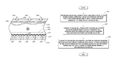
- the first operation 301 can include providing a solar cell having a front side which faces the sun during normal operation, a back side opposite the front side, a texturized region and a lightly doped diffusion region on the front side of the solar cell.
- a second operation 302 can include forming a first protective layer on the front side of the solar cell.
- a third operation 303 can include placing the solar cell on a receiving medium with the front side of the solar cell placed on an upper surface of the receiving medium.
- a fourth operation can include depositing the first etch resist on the back side of the solar cell using a contact printing method, where the first protective layer prevents damage to the texturized region and the lightly doped diffusion on the front side of the solar cell during the printing process.
- a fifth operation 305 can include removing the solar cell from the receiving medium.
- the last operation can include curing the first etch resist.
- the first etch resist is a plating resist.
- depositing the first etch resist comprises screen printing the first etch resist.
- the curing the first etch resist comprises performing a method selected from the group consisting of thermal cure and photo-curing.
- forming the first protective layer further includes depositing a second etch resist on the front side of the solar cell prior to forming a first etch resist and curing the second etch resist to form a first protective layer on the front side of the solar cell.
- forming the first protective layer comprises a depositing silicon nitride (SiN) with a thickness in the range of 100-3000 Angstroms on the front side of the solar cell.
- the method for forming a first etch resist on a solar cell is employed for any applicable solar cell fabrication printing, masking or applicable process which subsequently provides a solar cell with a texturized region and a lightly doped diffusion region and as defined herein.
- FIG. 13 illustrates a flowchart of another method for forming a first etch resist on a solar cell.
- the first operation 311 can include providing a solar cell having a front side which faces the sun during normal operation, a back side opposite the front side, a texturized region and a lightly doped diffusion region on the front side of the solar cell.
- a second operation 312 can include placing the solar cell on a receiving medium with the front side of the solar cell placed on an upper surface of the receiving medium.
- a third operation 313 can include depositing the first etch resist on the back side of the solar cell using a contact printing method, where the upper surface of the receiving medium prevents damage to the texturized region and the lightly doped diffusion.
- a fourth operation 314 can include removing the solar cell from the receiving medium and a last operation 315 can include curing the first etch resist.
- the lightly doped diffusion region has a doping concentration below 1 ⁇ 10 19 cm ⁇ 3 .
- the lightly doped diffusion region has a doping concentration in the range of 1 ⁇ 10 17 -1 ⁇ 10 19 cm ⁇ 3 .
- the lightly doped diffusion region extends less than 1 micron into the silicon substrate.
- the receiving medium comprises a material having a mohs hardness in the range of 5-10.
- the upper surface of the receiving medium prevents damage to the texturized region and the lightly doped diffusion region during printing after between 1-50,000 uses.
- the upper surface of the receiving medium maintains a constant planarity after between 1-50,000 uses.
- the receiving medium comprises a material selected from the group consisting of acrylic, aluminum, anodized aluminum, hard anodized aluminum, glass and tempered glass.
- depositing the first etch resist comprises screen printing the first etch resist.
- the method for forming a first etch resist on a solar cell is employed for any applicable solar cell fabrication printing, masking or applicable process which subsequently provides a solar cell with a texturized region and a lightly doped diffusion region and as defined herein.
- the first operation 321 can include providing a solar cell having a front side which faces the sun during normal operation, a back side opposite the front side, a texturized region and a lightly doped diffusion region on the front side of the solar cell.
- a second operation 322 can include forming a first protective layer on the front side of the solar cell, where the first protective layer prevents damage to a texturized region and a lightly doped diffusion on the front side of the solar cell during a pick-and-place operation.
- a third operation 323 can include picking the solar cell from a first location on a first receiving medium using a contact transfer tool, where a bottom surface of the contact transfer tool contacts the front side of the solar cell.
- a last operation 324 can include placing the solar cell on a second location on a second receiving medium using the contact transfer tool.
- forming the first protective layer includes depositing a second etch resist on the front side of the solar cell and curing the second etch resist to form a first protective layer on the front side of the solar cell.
- the second etch resist is any etch resist commonly used in the fabrication of solar cells.
- depositing the second etch resist comprises screen printing the second etch resist.
- the curing the second etch resist comprises photo-curing the second etch resist.
- forming the first protective layer comprises forming a first dielectric layer on the front side of the solar cell.
- forming the first dielectric layer comprises depositing an anti-reflective layer commonly used in the manufacture of solar cells.
- forming the first dielectric layer comprises depositing silicon nitride (SiN) on the front side of the solar cell.
- forming the first dielectric layer comprises a depositing silicon nitride (SiN) with a thickness in the range of 100-3000 Angstroms.
- the lightly doped diffusion region has a doping concentration below 1 ⁇ 10 19 cm ⁇ 3 .
- the lightly doped diffusion region has a doping concentration in the range of 1 ⁇ 10 17 -1 ⁇ 10 19 cm ⁇ 3 . In yet another embodiment, lightly doped diffusion region extends less than 1 micron into the silicon substrate.
- the first and second receiving mediums comprise a receiving medium selected from the group consisting of chuck, palette, jig, walking beam, mount and conveyor.
- the method for transferring a solar cell from a first location to a second location is employed for any applicable solar cell fabrication, transport or transfer process which subsequently provides a solar cell with a texturized region and a lightly doped diffusion region and as defined herein.
- FIG. 15 illustrates a flowchart for another method of transferring a solar cell from a first location to a second location.
- the first operation 331 can includes providing a solar cell having a front side which faces the sun during normal operation, a back side opposite the front side, a texturized region and a lightly doped diffusion region on the front side of the solar cell.
- a second operation 332 can include picking the solar cell from a first location on a first receiving medium using a contact transfer tool, where a bottom surface of the contact transfer tool contacts the front side of the solar cell.
- a last operation 313 can include placing the solar cell on a second location on a second receiving medium using the contact transfer tool, where the bottom surface of the contact transfer tool prevents damage to the texturized region and the lightly doped diffusion region during a pick-and-place operation.
- the lightly doped diffusion region has a doping concentration below 1 ⁇ 10 19 cm ⁇ 3 .
- the lightly doped diffusion region has a doping concentration in the range of 1 ⁇ 10 17 -1 ⁇ 10 19 cm ⁇ 3 .
- the lightly doped diffusion region has a doping concentration in the range of 1 ⁇ 10 17 -1 ⁇ 10 19 cm ⁇ 3 .
- the receiving medium comprises a material having a moh's hardness in the range of 5-10.
- the upper surface of the receiving medium prevents damage to the texturized region during printing after between 1-50,000 uses. In another embodiment, the upper surface of the receiving medium maintains a constant planarity after between 1-50,000 uses.
- the receiving medium comprises a material selected from the group consisting of acrylic, aluminum, anodized aluminum, hard anodized aluminum, glass and tempered glass. In yet another embodiment, the receiving medium comprises a receiving medium selected from the group consisting of chuck, palette, jig, walking beam, mount and conveyor.
- the method for transferring a solar cell from a first location to a second location is employed for any applicable solar cell fabrication, transport or transfer process which subsequently provides a solar cell with a texturized region and a lightly doped diffusion region and as defined herein.
- the first operation 341 can include providing a solar cell having a front side which faces the sun during normal operation and a back side opposite the front side.
- a second operation 342 can include forming a doped region on a silicon substrate of the solar cell.
- a third operation 343 can include etching a texturized region on the silicon substrate.
- a fourth operation can include forming a lightly doped diffusion region on the silicon substrate, where the lightly doped diffusion region is formed on the same side as texturized region on the silicon substrate on.
- a fifth operation 345 can include forming a first protective layer over texturized region and lightly doped diffusion region, where the first protective layer prevents damage to the texturized region and lightly doped diffusion region during manufacturing.
- a sixth operation 346 can include depositing a dielectric layer over the texturized region and lightly doped diffusion region and the doped region.
- a seventh operation can include forming a plurality of contact openings through the dielectric layer.
- a last operation 318 can include forming a first metal grid electrically coupled to the doped region through the contact openings and a second metal grid being electrically coupled to the first metal grid.
- forming the first protective layer further includes depositing a second etch resist on the front side of the solar cell prior to forming a first etch resist and curing the second etch resist to form a first protective layer on the front side of the solar cell.
- the second etch resist is any standard etch resist used in the manufacturing or fabrication of solar cells.
- FIG. 17 illustrates a flowchart for another method of manufacturing a solar cell.
- the first operation 351 can include providing a solar cell having a front side which faces the sun during normal operation and a back side opposite the front side.
- a second operation 352 can include forming a doped region on a silicon substrate of the solar cell.
- a third operation 353 can include etching a texturized region on the silicon substrate.
- a fourth operation 354 can include forming a lightly doped diffusion region on the silicon substrate, where the lightly doped diffusion region is formed on the same side as texturized region on the silicon substrate.
- a fifth operation 355 can include depositing a first dielectric layer over the texturized region and lightly doped diffusion region, where the first dielectric layer prevents damage to the texturized region and lightly doped diffusion region during manufacturing.
- a sixth operation 356 can include depositing a second dielectric layer over the doped region.
- a seventh operation 357 can include forming a plurality of contact openings through the second dielectric layer.
- a last operation 358 can include forming a first metal grid electrically coupled to the doped region through the contact openings and a second metal grid being electrically coupled to the first metal grid.
- forming the first dielectric layer comprises a depositing silicon nitride (SiN) with a thickness in the range of 100-3000 Angstroms on the front side of the solar cell.
Landscapes
- Photovoltaic Devices (AREA)
- Engineering & Computer Science (AREA)
- Manufacturing & Machinery (AREA)
- Life Sciences & Earth Sciences (AREA)
- Sustainable Development (AREA)
- Sustainable Energy (AREA)
Abstract
Description
Claims (20)
Priority Applications (9)
| Application Number | Priority Date | Filing Date | Title |
|---|---|---|---|
| US13/837,802 US8901010B2 (en) | 2013-03-15 | 2013-03-15 | Methods for improving solar cell lifetime and efficiency |
| AU2014236652A AU2014236652B2 (en) | 2013-03-15 | 2014-03-13 | Methods for improving solar cell lifetime and efficiency |
| JP2016502235A JP2016512396A (en) | 2013-03-15 | 2014-03-13 | Method for improving the lifetime and efficiency of solar cells |
| MYPI2015002245A MY172753A (en) | 2013-03-15 | 2014-03-13 | Methods for improving solar cell lifetime and efficiency |
| KR1020157028798A KR102242268B1 (en) | 2013-03-15 | 2014-03-13 | Methods for improving solar cell lifetime and efficiency |
| CN201480012458.7A CN105409008B (en) | 2013-03-15 | 2014-03-13 | Method for improving solar cell lifetime and efficiency |
| PCT/US2014/026765 WO2014151981A1 (en) | 2013-03-15 | 2014-03-13 | Methods for improving solar cell lifetime and efficiency |
| DE112014001412.5T DE112014001412T5 (en) | 2013-03-15 | 2014-03-13 | Method for improving the life and efficiency of solar cells |
| TW103109808A TWI606602B (en) | 2013-03-15 | 2014-03-14 | Method for improving solar cell life and efficiency |
Applications Claiming Priority (1)
| Application Number | Priority Date | Filing Date | Title |
|---|---|---|---|
| US13/837,802 US8901010B2 (en) | 2013-03-15 | 2013-03-15 | Methods for improving solar cell lifetime and efficiency |
Publications (2)
| Publication Number | Publication Date |
|---|---|
| US20140273326A1 US20140273326A1 (en) | 2014-09-18 |
| US8901010B2 true US8901010B2 (en) | 2014-12-02 |
Family
ID=51528896
Family Applications (1)
| Application Number | Title | Priority Date | Filing Date |
|---|---|---|---|
| US13/837,802 Active US8901010B2 (en) | 2013-03-15 | 2013-03-15 | Methods for improving solar cell lifetime and efficiency |
Country Status (9)
| Country | Link |
|---|---|
| US (1) | US8901010B2 (en) |
| JP (1) | JP2016512396A (en) |
| KR (1) | KR102242268B1 (en) |
| CN (1) | CN105409008B (en) |
| AU (1) | AU2014236652B2 (en) |
| DE (1) | DE112014001412T5 (en) |
| MY (1) | MY172753A (en) |
| TW (1) | TWI606602B (en) |
| WO (1) | WO2014151981A1 (en) |
Cited By (12)
| Publication number | Priority date | Publication date | Assignee | Title |
|---|---|---|---|---|
| USD822890S1 (en) | 2016-09-07 | 2018-07-10 | Felxtronics Ap, Llc | Lighting apparatus |
| USD832495S1 (en) | 2017-08-18 | 2018-10-30 | Flex Ltd. | Lighting module locking mechanism |
| USD832494S1 (en) | 2017-08-09 | 2018-10-30 | Flex Ltd. | Lighting module heatsink |
| USD833061S1 (en) | 2017-08-09 | 2018-11-06 | Flex Ltd. | Lighting module locking endcap |
| USD846793S1 (en) | 2017-08-09 | 2019-04-23 | Flex Ltd. | Lighting module locking mechanism |
| USD862777S1 (en) | 2017-08-09 | 2019-10-08 | Flex Ltd. | Lighting module wide distribution lens |
| USD862778S1 (en) | 2017-08-22 | 2019-10-08 | Flex Ltd | Lighting module lens |
| USD872319S1 (en) | 2017-08-09 | 2020-01-07 | Flex Ltd. | Lighting module LED light board |
| USD877964S1 (en) | 2017-08-09 | 2020-03-10 | Flex Ltd. | Lighting module |
| USD888323S1 (en) | 2017-09-07 | 2020-06-23 | Flex Ltd | Lighting module wire guard |
| US10775030B2 (en) | 2017-05-05 | 2020-09-15 | Flex Ltd. | Light fixture device including rotatable light modules |
| CN114649441A (en) * | 2020-12-21 | 2022-06-21 | 株式会社钟化 | Method for manufacturing solar cell |
Families Citing this family (2)
| Publication number | Priority date | Publication date | Assignee | Title |
|---|---|---|---|---|
| TWI550886B (en) * | 2015-07-10 | 2016-09-21 | 國立屏東科技大學 | 矽 substrate surface roughening method |
| US10224268B1 (en) * | 2016-11-28 | 2019-03-05 | CoolStar Technology, Inc. | Enhanced thermal transfer in a semiconductor structure |
Citations (6)
| Publication number | Priority date | Publication date | Assignee | Title |
|---|---|---|---|---|
| US4029518A (en) * | 1974-11-20 | 1977-06-14 | Sharp Kabushiki Kaisha | Solar cell |
| US4131488A (en) * | 1975-12-31 | 1978-12-26 | Motorola, Inc. | Method of semiconductor solar energy device fabrication |
| US4252865A (en) * | 1978-05-24 | 1981-02-24 | National Patent Development Corporation | Highly solar-energy absorbing device and method of making the same |
| US4322571A (en) * | 1980-07-17 | 1982-03-30 | The Boeing Company | Solar cells and methods for manufacture thereof |
| US7557367B2 (en) * | 2004-06-04 | 2009-07-07 | The Board Of Trustees Of The University Of Illinois | Stretchable semiconductor elements and stretchable electrical circuits |
| US8084293B2 (en) * | 2010-04-06 | 2011-12-27 | Varian Semiconductor Equipment Associates, Inc. | Continuously optimized solar cell metallization design through feed-forward process |
Family Cites Families (24)
| Publication number | Priority date | Publication date | Assignee | Title |
|---|---|---|---|---|
| JPH0680635B2 (en) * | 1989-01-30 | 1994-10-12 | 信越半導体株式会社 | Method for forming backside sealing film for preventing autodoping |
| JPH02291108A (en) * | 1989-04-28 | 1990-11-30 | Nippon Steel Corp | Vacuum chuck for resist coating apparatus and resist coater |
| JP2779968B2 (en) * | 1989-12-29 | 1998-07-23 | 東陶機器株式会社 | Vacuum chuck |
| JPH0681171A (en) * | 1991-05-30 | 1994-03-22 | New Japan Radio Co Ltd | Selective etching method of oxidized film on wafer |
| JP3360919B2 (en) * | 1993-06-11 | 2003-01-07 | 三菱電機株式会社 | Method of manufacturing thin-film solar cell and thin-film solar cell |
| US7388147B2 (en) * | 2003-04-10 | 2008-06-17 | Sunpower Corporation | Metal contact structure for solar cell and method of manufacture |
| US7094709B2 (en) * | 2004-06-15 | 2006-08-22 | Braggone Oy | Method of synthesizing hybrid metal oxide materials and applications thereof |
| CN101496155B (en) * | 2006-03-31 | 2010-07-28 | Afco股份公司 | Apparatus and method for metallizing a substrate of a photovoltaic cell |
| JP2007281044A (en) * | 2006-04-04 | 2007-10-25 | Canon Inc | Solar cell |
| US7811900B2 (en) * | 2006-09-08 | 2010-10-12 | Silicon Genesis Corporation | Method and structure for fabricating solar cells using a thick layer transfer process |
| US8035028B2 (en) * | 2006-10-09 | 2011-10-11 | Solexel, Inc. | Pyramidal three-dimensional thin-film solar cells |
| US8084684B2 (en) * | 2006-10-09 | 2011-12-27 | Solexel, Inc. | Three-dimensional thin-film solar cells |
| US8322300B2 (en) * | 2008-02-07 | 2012-12-04 | Sunpower Corporation | Edge coating apparatus with movable roller applicator for solar cell substrates |
| KR100954367B1 (en) * | 2008-04-17 | 2010-04-26 | (주)텔리오솔라코리아 | Patterning Device for Solar Cell Manufacturing |
| EP2280813B1 (en) * | 2008-04-18 | 2017-06-07 | Massachusetts Institute Of Technology | Imprint patterning of irregular surface |
| US8062693B2 (en) * | 2008-09-22 | 2011-11-22 | Sunpower Corporation | Generation of contact masks for inkjet printing on solar cell substrates |
| US8525018B2 (en) * | 2009-09-07 | 2013-09-03 | Lg Electronics Inc. | Solar cell |
| KR101027829B1 (en) * | 2010-01-18 | 2011-04-07 | 현대중공업 주식회사 | Manufacturing method of back electrode solar cell |
| JP5754890B2 (en) * | 2010-03-30 | 2015-07-29 | 京セラ株式会社 | Screen printing method |
| EP2395554A3 (en) * | 2010-06-14 | 2015-03-11 | Imec | Fabrication method for interdigitated back contact photovoltaic cells |
| CN103348491A (en) * | 2010-12-29 | 2013-10-09 | Gtat公司 | Method to form device by constructing support element on thin semiconductor lamina |
| JP6127047B2 (en) * | 2011-08-04 | 2017-05-10 | アイメックImec | Interdigitated electrode formation |
| WO2013024746A1 (en) * | 2011-08-12 | 2013-02-21 | Kobayashi Hikaru | Method for manufacturing semiconductor device, device for manufacturing semiconductor device, semiconductor device, program for manufacturing semiconductor device, treatment agent for semiconductor, and transfer member |
| JP2012144049A (en) * | 2012-04-04 | 2012-08-02 | Mitsubishi Electric Corp | Screen printing machine |
-
2013
- 2013-03-15 US US13/837,802 patent/US8901010B2/en active Active
-
2014
- 2014-03-13 WO PCT/US2014/026765 patent/WO2014151981A1/en not_active Ceased
- 2014-03-13 KR KR1020157028798A patent/KR102242268B1/en active Active
- 2014-03-13 DE DE112014001412.5T patent/DE112014001412T5/en not_active Withdrawn
- 2014-03-13 MY MYPI2015002245A patent/MY172753A/en unknown
- 2014-03-13 AU AU2014236652A patent/AU2014236652B2/en not_active Ceased
- 2014-03-13 CN CN201480012458.7A patent/CN105409008B/en active Active
- 2014-03-13 JP JP2016502235A patent/JP2016512396A/en active Pending
- 2014-03-14 TW TW103109808A patent/TWI606602B/en not_active IP Right Cessation
Patent Citations (6)
| Publication number | Priority date | Publication date | Assignee | Title |
|---|---|---|---|---|
| US4029518A (en) * | 1974-11-20 | 1977-06-14 | Sharp Kabushiki Kaisha | Solar cell |
| US4131488A (en) * | 1975-12-31 | 1978-12-26 | Motorola, Inc. | Method of semiconductor solar energy device fabrication |
| US4252865A (en) * | 1978-05-24 | 1981-02-24 | National Patent Development Corporation | Highly solar-energy absorbing device and method of making the same |
| US4322571A (en) * | 1980-07-17 | 1982-03-30 | The Boeing Company | Solar cells and methods for manufacture thereof |
| US7557367B2 (en) * | 2004-06-04 | 2009-07-07 | The Board Of Trustees Of The University Of Illinois | Stretchable semiconductor elements and stretchable electrical circuits |
| US8084293B2 (en) * | 2010-04-06 | 2011-12-27 | Varian Semiconductor Equipment Associates, Inc. | Continuously optimized solar cell metallization design through feed-forward process |
Cited By (20)
| Publication number | Priority date | Publication date | Assignee | Title |
|---|---|---|---|---|
| USD822890S1 (en) | 2016-09-07 | 2018-07-10 | Felxtronics Ap, Llc | Lighting apparatus |
| US10775030B2 (en) | 2017-05-05 | 2020-09-15 | Flex Ltd. | Light fixture device including rotatable light modules |
| USD853629S1 (en) | 2017-08-09 | 2019-07-09 | Flex Ltd | Lighting module locking mechanism |
| USD905325S1 (en) | 2017-08-09 | 2020-12-15 | Flex Ltd | Lighting module |
| USD846793S1 (en) | 2017-08-09 | 2019-04-23 | Flex Ltd. | Lighting module locking mechanism |
| USD832494S1 (en) | 2017-08-09 | 2018-10-30 | Flex Ltd. | Lighting module heatsink |
| USD853627S1 (en) | 2017-08-09 | 2019-07-09 | Flex Ltd | Lighting module locking endcap |
| USD833061S1 (en) | 2017-08-09 | 2018-11-06 | Flex Ltd. | Lighting module locking endcap |
| USD853625S1 (en) | 2017-08-09 | 2019-07-09 | Flex Ltd | Lighting module heatsink |
| USD862777S1 (en) | 2017-08-09 | 2019-10-08 | Flex Ltd. | Lighting module wide distribution lens |
| USD1010915S1 (en) | 2017-08-09 | 2024-01-09 | Linmore Labs Led, Inc. | Lighting module |
| USD872319S1 (en) | 2017-08-09 | 2020-01-07 | Flex Ltd. | Lighting module LED light board |
| USD877964S1 (en) | 2017-08-09 | 2020-03-10 | Flex Ltd. | Lighting module |
| USD885615S1 (en) | 2017-08-09 | 2020-05-26 | Flex Ltd. | Lighting module LED light board |
| USD853628S1 (en) | 2017-08-18 | 2019-07-09 | Flex Ltd. | Lighting module locking mechanism |
| USD832495S1 (en) | 2017-08-18 | 2018-10-30 | Flex Ltd. | Lighting module locking mechanism |
| USD862778S1 (en) | 2017-08-22 | 2019-10-08 | Flex Ltd | Lighting module lens |
| USD888323S1 (en) | 2017-09-07 | 2020-06-23 | Flex Ltd | Lighting module wire guard |
| CN114649441A (en) * | 2020-12-21 | 2022-06-21 | 株式会社钟化 | Method for manufacturing solar cell |
| CN114649441B (en) * | 2020-12-21 | 2023-11-14 | 株式会社钟化 | Method for manufacturing solar cell |
Also Published As
| Publication number | Publication date |
|---|---|
| CN105409008B (en) | 2017-07-14 |
| KR20150132323A (en) | 2015-11-25 |
| US20140273326A1 (en) | 2014-09-18 |
| CN105409008A (en) | 2016-03-16 |
| JP2016512396A (en) | 2016-04-25 |
| MY172753A (en) | 2019-12-11 |
| WO2014151981A1 (en) | 2014-09-25 |
| TW201448259A (en) | 2014-12-16 |
| KR102242268B1 (en) | 2021-04-19 |
| DE112014001412T5 (en) | 2015-12-17 |
| AU2014236652A1 (en) | 2015-08-20 |
| AU2014236652B2 (en) | 2017-12-07 |
| TWI606602B (en) | 2017-11-21 |
Similar Documents
| Publication | Publication Date | Title |
|---|---|---|
| US8901010B2 (en) | Methods for improving solar cell lifetime and efficiency | |
| TWI559563B (en) | Hybrid polycrystalline germanium heterojunction back contact battery | |
| CN102239572B (en) | Be formed with the back contact solar cells of polysilicon doped regions | |
| US6998288B1 (en) | Use of doped silicon dioxide in the fabrication of solar cells | |
| US8822257B2 (en) | Thin silicon solar cell and method of manufacture | |
| CN102959715B (en) | Fabrication of solar cells with protection against compensating doping | |
| US9640676B2 (en) | Methods and structures for improving the structural integrity of solar cells | |
| JP6690859B2 (en) | Relative dopant concentration level in solar cells | |
| US20200212230A1 (en) | Leakage pathway layer for solar cell | |
| US10326031B2 (en) | Method of patterning an amorphous semiconductor layer | |
| EP4557386A1 (en) | Solar cell and manufacturing method therefor | |
| US10861987B2 (en) | Method for manufacturing selective emitter using surface structure and solar cell including selective emitter using surface structure | |
| US10593824B2 (en) | Ultra-thin flexible rear-contact Si solar cells and methods for manufacturing the same | |
| KR101160116B1 (en) | Method of manufacturing Back junction solar cell | |
| KR20100073645A (en) | Solar cell and method for manufacturing thereof | |
| KR101161807B1 (en) | Method of manufacturing Back junction solar cell by using plasma doping and diffusion and the solar cell | |
| US9842956B2 (en) | System and method for mass-production of high-efficiency photovoltaic structures | |
| CN118431343A (en) | Solar cell and method for manufacturing the same | |
| US8871608B2 (en) | Method for fabricating backside-illuminated sensors | |
| Chithambaranadhan et al. | Efficiency improvement in nonprime crystalline Silicon solar cells by chemical isolation of shunts under front metallization |
Legal Events
| Date | Code | Title | Description |
|---|---|---|---|
| AS | Assignment |
Owner name: SUNPOWER CORPORATION, CALIFORNIA Free format text: ASSIGNMENT OF ASSIGNORS INTEREST;ASSIGNORS:WESTERBERG, STAFFAN;VICENTE, FLORITO DENNIS TINGCHUY;CUDZINOVIC, MICHAEL;AND OTHERS;SIGNING DATES FROM 20131107 TO 20140525;REEL/FRAME:032977/0349 |
|
| STCF | Information on status: patent grant |
Free format text: PATENTED CASE |
|
| MAFP | Maintenance fee payment |
Free format text: PAYMENT OF MAINTENANCE FEE, 4TH YEAR, LARGE ENTITY (ORIGINAL EVENT CODE: M1551) Year of fee payment: 4 |
|
| MAFP | Maintenance fee payment |
Free format text: PAYMENT OF MAINTENANCE FEE, 8TH YEAR, LARGE ENTITY (ORIGINAL EVENT CODE: M1552); ENTITY STATUS OF PATENT OWNER: LARGE ENTITY Year of fee payment: 8 |
|
| AS | Assignment |
Owner name: MAXEON SOLAR PTE. LTD., SINGAPORE Free format text: ASSIGNMENT OF ASSIGNORS INTEREST;ASSIGNOR:SUNPOWER CORPORATION;REEL/FRAME:062699/0875 Effective date: 20221214 |
|
| AS | Assignment |
Owner name: DB TRUSTEES (HONG KONG) LIMITED, HONG KONG Free format text: SECURITY INTEREST;ASSIGNOR:MAXEON SOLAR PTE. LTD.;REEL/FRAME:067637/0598 Effective date: 20240531 |
|
| AS | Assignment |
Owner name: DB TRUSTEES (HONG KONG) LIMITED, HONG KONG Free format text: SECOND LIEN SECURITY INTEREST AGREEMENT;ASSIGNOR:MAXEON SOLAR PTE. LTD;REEL/FRAME:071343/0553 Effective date: 20240620 |
|
| AS | Assignment |
Owner name: DB TRUSTEES (HONG KONG) LIMITED, HONG KONG Free format text: SECURITY INTEREST;ASSIGNOR:MAXEON SOLAR PTE. LTD.;REEL/FRAME:067924/0062 Effective date: 20240620 |