EP2514049B1 - Procédé de fabrication d'éléments électroluminescents semi-conducteurs - Google Patents
Procédé de fabrication d'éléments électroluminescents semi-conducteurs Download PDFInfo
- Publication number
- EP2514049B1 EP2514049B1 EP10779771.4A EP10779771A EP2514049B1 EP 2514049 B1 EP2514049 B1 EP 2514049B1 EP 10779771 A EP10779771 A EP 10779771A EP 2514049 B1 EP2514049 B1 EP 2514049B1
- Authority
- EP
- European Patent Office
- Prior art keywords
- ridge
- shaped region
- semiconductor
- semiconductor body
- web
- Prior art date
- Legal status (The legal status is an assumption and is not a legal conclusion. Google has not performed a legal analysis and makes no representation as to the accuracy of the status listed.)
- Active
Links
- 239000004065 semiconductor Substances 0.000 title claims description 172
- 238000004519 manufacturing process Methods 0.000 title claims description 17
- 238000000034 method Methods 0.000 title claims description 13
- 230000005855 radiation Effects 0.000 claims description 27
- 230000003287 optical effect Effects 0.000 claims description 3
- 238000000151 deposition Methods 0.000 claims description 2
- 239000000758 substrate Substances 0.000 description 20
- 239000013078 crystal Substances 0.000 description 12
- 239000000463 material Substances 0.000 description 11
- 238000000926 separation method Methods 0.000 description 6
- 150000001875 compounds Chemical class 0.000 description 5
- -1 nitride compound Chemical class 0.000 description 4
- 230000003595 spectral effect Effects 0.000 description 4
- JMASRVWKEDWRBT-UHFFFAOYSA-N Gallium nitride Chemical compound [Ga]#N JMASRVWKEDWRBT-UHFFFAOYSA-N 0.000 description 3
- 238000005253 cladding Methods 0.000 description 3
- 239000011248 coating agent Substances 0.000 description 3
- 238000000576 coating method Methods 0.000 description 3
- 230000001427 coherent effect Effects 0.000 description 3
- 150000004767 nitrides Chemical class 0.000 description 3
- 238000002310 reflectometry Methods 0.000 description 3
- 239000000126 substance Substances 0.000 description 3
- PXHVJJICTQNCMI-UHFFFAOYSA-N Nickel Chemical compound [Ni] PXHVJJICTQNCMI-UHFFFAOYSA-N 0.000 description 2
- KDLHZDBZIXYQEI-UHFFFAOYSA-N Palladium Chemical compound [Pd] KDLHZDBZIXYQEI-UHFFFAOYSA-N 0.000 description 2
- 229910052782 aluminium Inorganic materials 0.000 description 2
- 238000003486 chemical etching Methods 0.000 description 2
- 239000000470 constituent Substances 0.000 description 2
- 238000006073 displacement reaction Methods 0.000 description 2
- 238000009826 distribution Methods 0.000 description 2
- 238000009413 insulation Methods 0.000 description 2
- 229910052751 metal Inorganic materials 0.000 description 2
- 239000002184 metal Substances 0.000 description 2
- 238000002488 metal-organic chemical vapour deposition Methods 0.000 description 2
- BASFCYQUMIYNBI-UHFFFAOYSA-N platinum Chemical compound [Pt] BASFCYQUMIYNBI-UHFFFAOYSA-N 0.000 description 2
- VYZAMTAEIAYCRO-UHFFFAOYSA-N Chromium Chemical compound [Cr] VYZAMTAEIAYCRO-UHFFFAOYSA-N 0.000 description 1
- 229910002601 GaN Inorganic materials 0.000 description 1
- 229910052581 Si3N4 Inorganic materials 0.000 description 1
- VYPSYNLAJGMNEJ-UHFFFAOYSA-N Silicium dioxide Chemical compound O=[Si]=O VYPSYNLAJGMNEJ-UHFFFAOYSA-N 0.000 description 1
- XUIMIQQOPSSXEZ-UHFFFAOYSA-N Silicon Chemical compound [Si] XUIMIQQOPSSXEZ-UHFFFAOYSA-N 0.000 description 1
- BQCADISMDOOEFD-UHFFFAOYSA-N Silver Chemical compound [Ag] BQCADISMDOOEFD-UHFFFAOYSA-N 0.000 description 1
- GWEVSGVZZGPLCZ-UHFFFAOYSA-N Titan oxide Chemical compound O=[Ti]=O GWEVSGVZZGPLCZ-UHFFFAOYSA-N 0.000 description 1
- RTAQQCXQSZGOHL-UHFFFAOYSA-N Titanium Chemical compound [Ti] RTAQQCXQSZGOHL-UHFFFAOYSA-N 0.000 description 1
- XAGFODPZIPBFFR-UHFFFAOYSA-N aluminium Chemical compound [Al] XAGFODPZIPBFFR-UHFFFAOYSA-N 0.000 description 1
- 230000015572 biosynthetic process Effects 0.000 description 1
- 239000002800 charge carrier Substances 0.000 description 1
- 229910052804 chromium Inorganic materials 0.000 description 1
- 239000011651 chromium Substances 0.000 description 1
- 239000002131 composite material Substances 0.000 description 1
- 230000007423 decrease Effects 0.000 description 1
- 230000007547 defect Effects 0.000 description 1
- 230000001419 dependent effect Effects 0.000 description 1
- 230000008021 deposition Effects 0.000 description 1
- 238000001514 detection method Methods 0.000 description 1
- 238000011161 development Methods 0.000 description 1
- 230000018109 developmental process Effects 0.000 description 1
- 239000006185 dispersion Substances 0.000 description 1
- 239000002019 doping agent Substances 0.000 description 1
- 238000005516 engineering process Methods 0.000 description 1
- 230000002349 favourable effect Effects 0.000 description 1
- 229910052733 gallium Inorganic materials 0.000 description 1
- PCHJSUWPFVWCPO-UHFFFAOYSA-N gold Chemical compound [Au] PCHJSUWPFVWCPO-UHFFFAOYSA-N 0.000 description 1
- 229910052737 gold Inorganic materials 0.000 description 1
- 239000010931 gold Substances 0.000 description 1
- 230000005484 gravity Effects 0.000 description 1
- 229910052738 indium Inorganic materials 0.000 description 1
- 229910001092 metal group alloy Inorganic materials 0.000 description 1
- 150000002739 metals Chemical class 0.000 description 1
- 239000000203 mixture Substances 0.000 description 1
- 229910052759 nickel Inorganic materials 0.000 description 1
- 229910052757 nitrogen Inorganic materials 0.000 description 1
- 229910052763 palladium Inorganic materials 0.000 description 1
- 230000000737 periodic effect Effects 0.000 description 1
- 230000000704 physical effect Effects 0.000 description 1
- 229910052697 platinum Inorganic materials 0.000 description 1
- 229910052703 rhodium Inorganic materials 0.000 description 1
- 239000010948 rhodium Substances 0.000 description 1
- MHOVAHRLVXNVSD-UHFFFAOYSA-N rhodium atom Chemical compound [Rh] MHOVAHRLVXNVSD-UHFFFAOYSA-N 0.000 description 1
- 238000006748 scratching Methods 0.000 description 1
- 230000002393 scratching effect Effects 0.000 description 1
- 229910052710 silicon Inorganic materials 0.000 description 1
- 239000010703 silicon Substances 0.000 description 1
- HQVNEWCFYHHQES-UHFFFAOYSA-N silicon nitride Chemical compound N12[Si]34N5[Si]62N3[Si]51N64 HQVNEWCFYHHQES-UHFFFAOYSA-N 0.000 description 1
- 229910052814 silicon oxide Inorganic materials 0.000 description 1
- 229910052709 silver Inorganic materials 0.000 description 1
- 239000004332 silver Substances 0.000 description 1
- 238000004544 sputter deposition Methods 0.000 description 1
- 229910052719 titanium Inorganic materials 0.000 description 1
- 239000010936 titanium Substances 0.000 description 1
- OGIDPMRJRNCKJF-UHFFFAOYSA-N titanium oxide Inorganic materials [Ti]=O OGIDPMRJRNCKJF-UHFFFAOYSA-N 0.000 description 1
- 238000007740 vapor deposition Methods 0.000 description 1
Images

Classifications
-
- H—ELECTRICITY
- H01—ELECTRIC ELEMENTS
- H01S—DEVICES USING THE PROCESS OF LIGHT AMPLIFICATION BY STIMULATED EMISSION OF RADIATION [LASER] TO AMPLIFY OR GENERATE LIGHT; DEVICES USING STIMULATED EMISSION OF ELECTROMAGNETIC RADIATION IN WAVE RANGES OTHER THAN OPTICAL
- H01S5/00—Semiconductor lasers
- H01S5/30—Structure or shape of the active region; Materials used for the active region
- H01S5/32—Structure or shape of the active region; Materials used for the active region comprising PN junctions, e.g. hetero- or double- heterostructures
- H01S5/323—Structure or shape of the active region; Materials used for the active region comprising PN junctions, e.g. hetero- or double- heterostructures in AIIIBV compounds, e.g. AlGaAs-laser, InP-based laser
- H01S5/32308—Structure or shape of the active region; Materials used for the active region comprising PN junctions, e.g. hetero- or double- heterostructures in AIIIBV compounds, e.g. AlGaAs-laser, InP-based laser emitting light at a wavelength less than 900 nm
- H01S5/32341—Structure or shape of the active region; Materials used for the active region comprising PN junctions, e.g. hetero- or double- heterostructures in AIIIBV compounds, e.g. AlGaAs-laser, InP-based laser emitting light at a wavelength less than 900 nm blue laser based on GaN or GaP
-
- H—ELECTRICITY
- H01—ELECTRIC ELEMENTS
- H01S—DEVICES USING THE PROCESS OF LIGHT AMPLIFICATION BY STIMULATED EMISSION OF RADIATION [LASER] TO AMPLIFY OR GENERATE LIGHT; DEVICES USING STIMULATED EMISSION OF ELECTROMAGNETIC RADIATION IN WAVE RANGES OTHER THAN OPTICAL
- H01S5/00—Semiconductor lasers
- H01S5/02—Structural details or components not essential to laser action
- H01S5/0201—Separation of the wafer into individual elements, e.g. by dicing, cleaving, etching or directly during growth
-
- H—ELECTRICITY
- H01—ELECTRIC ELEMENTS
- H01S—DEVICES USING THE PROCESS OF LIGHT AMPLIFICATION BY STIMULATED EMISSION OF RADIATION [LASER] TO AMPLIFY OR GENERATE LIGHT; DEVICES USING STIMULATED EMISSION OF ELECTROMAGNETIC RADIATION IN WAVE RANGES OTHER THAN OPTICAL
- H01S2304/00—Special growth methods for semiconductor lasers
- H01S2304/12—Pendeo epitaxial lateral overgrowth [ELOG], e.g. for growing GaN based blue laser diodes
-
- H—ELECTRICITY
- H01—ELECTRIC ELEMENTS
- H01S—DEVICES USING THE PROCESS OF LIGHT AMPLIFICATION BY STIMULATED EMISSION OF RADIATION [LASER] TO AMPLIFY OR GENERATE LIGHT; DEVICES USING STIMULATED EMISSION OF ELECTROMAGNETIC RADIATION IN WAVE RANGES OTHER THAN OPTICAL
- H01S5/00—Semiconductor lasers
- H01S5/02—Structural details or components not essential to laser action
- H01S5/022—Mountings; Housings
- H01S5/0235—Method for mounting laser chips
- H01S5/02355—Fixing laser chips on mounts
- H01S5/0237—Fixing laser chips on mounts by soldering
-
- H—ELECTRICITY
- H01—ELECTRIC ELEMENTS
- H01S—DEVICES USING THE PROCESS OF LIGHT AMPLIFICATION BY STIMULATED EMISSION OF RADIATION [LASER] TO AMPLIFY OR GENERATE LIGHT; DEVICES USING STIMULATED EMISSION OF ELECTROMAGNETIC RADIATION IN WAVE RANGES OTHER THAN OPTICAL
- H01S5/00—Semiconductor lasers
- H01S5/04—Processes or apparatus for excitation, e.g. pumping, e.g. by electron beams
- H01S5/042—Electrical excitation ; Circuits therefor
- H01S5/0425—Electrodes, e.g. characterised by the structure
- H01S5/04256—Electrodes, e.g. characterised by the structure characterised by the configuration
-
- H—ELECTRICITY
- H01—ELECTRIC ELEMENTS
- H01S—DEVICES USING THE PROCESS OF LIGHT AMPLIFICATION BY STIMULATED EMISSION OF RADIATION [LASER] TO AMPLIFY OR GENERATE LIGHT; DEVICES USING STIMULATED EMISSION OF ELECTROMAGNETIC RADIATION IN WAVE RANGES OTHER THAN OPTICAL
- H01S5/00—Semiconductor lasers
- H01S5/20—Structure or shape of the semiconductor body to guide the optical wave ; Confining structures perpendicular to the optical axis, e.g. index or gain guiding, stripe geometry, broad area lasers, gain tailoring, transverse or lateral reflectors, special cladding structures, MQW barrier reflection layers
- H01S5/22—Structure or shape of the semiconductor body to guide the optical wave ; Confining structures perpendicular to the optical axis, e.g. index or gain guiding, stripe geometry, broad area lasers, gain tailoring, transverse or lateral reflectors, special cladding structures, MQW barrier reflection layers having a ridge or stripe structure
- H01S5/2201—Structure or shape of the semiconductor body to guide the optical wave ; Confining structures perpendicular to the optical axis, e.g. index or gain guiding, stripe geometry, broad area lasers, gain tailoring, transverse or lateral reflectors, special cladding structures, MQW barrier reflection layers having a ridge or stripe structure in a specific crystallographic orientation
Definitions
- the present patent relates to a method of manufacturing a semiconductor laser.
- An object underlying the present application is to provide a low-cost method for producing a semiconductor laser of high quality.
- the semiconductor laser comprises a semiconductor body having an active region provided for generating radiation and a web-shaped region.
- the web-shaped region has a longitudinal axis extending along an emission direction, wherein the longitudinal axis is offset in the transverse direction with respect to a central axis of the semiconductor body extending in the emission direction.
- a transverse direction is understood to mean a direction which runs perpendicular to the emission direction in the plane of the semiconductor layers of the semiconductor body.
- a central axis is understood to mean an axis which runs centrally with respect to two lateral surfaces which bound the semiconductor body in each case in the transverse direction, that is to say equidistant from these lateral surfaces.
- the web-shaped region thus has a greater distance in the transverse direction to one of these side surfaces than to the other side surface.
- the central axis of the semiconductor body and the longitudinal axis of the web-shaped area preferably run parallel or at least substantially parallel to one another, but are not congruent due to the offset in the transverse direction.
- An arrangement with an offset is here understood to mean a targeted spacing of the longitudinal axis from the central axis.
- the web-shaped region is formed in the semiconductor body.
- the web-shaped region of the waveguide can serve within the semiconductor body.
- the active region is at least partially disposed within the web-shaped region.
- the side surfaces of the web-shaped area bound the active area in the transverse direction.
- the active region can also be spaced apart from the web-shaped region in the vertical direction, that is to say in a direction extending perpendicular to the main extension plane of the semiconductor layer sequence of the semiconductor body.
- the web-shaped region is formed on the, in particular prefabricated, semiconductor body.
- the web-shaped region can be formed by means of a contact layer.
- the semiconductor body has a displacement gradient in the transverse direction. That is, the dislocation density of the semiconductor body is inhomogeneous, and the statistical distribution of dislocations varies in the transverse direction.
- a displacement gradient can occur in particular when using a growth substrate for the semiconductor layers of the semiconductor body, which itself has an inhomogeneous dislocation density.
- the longitudinal axis of the web-shaped region is arranged on the side of the central axis in which the dislocation density is lower.
- the longitudinal axis of the web-shaped region is preferably offset by at least 10 ⁇ m, preferably by at least 20 ⁇ m, for example by 30 ⁇ m or more, with respect to the center axis of the semiconductor body.
- the longitudinal axis of the web-shaped region is offset by at least 0.05 times, preferably by at least 0.1 times, an expansion of the semiconductor body in the transverse direction with respect to the central axis of the semiconductor body.
- a contact layer is arranged on the semiconductor body.
- the contact layer is provided in particular for the external electrical contacting of the active region from an upper side of the web-shaped region side facing.
- the contact layer can furthermore be designed as a multilayer.
- the contact layer preferably forms a contact surface laterally of the web-shaped region.
- the extent of the contact surface in the transverse direction is preferably at least in regions at least 0.3 times, particularly preferably at least 0.4 times, the extent of the semiconductor body.
- a comparatively large contact surface is available, which can be electrically contacted externally, for example, with a wire bond connection.
- a width, ie an extension in the transverse direction, of the semiconductor body of about 250 .mu.m can be achieved, for example, that the contact surface has a width of 80 .mu.m or more, preferably 100 .mu.m or more, so that a Drahtbonditati, for example, with a diameter the bonding ball between 50 microns and 80 microns, can be simplified with a sufficiently large distance from the web-shaped area can be formed. The risk of damage to the web-shaped area in the manufacture of the wire bond connection and the requirements for the accuracy of the wire bonding process are thereby reduced.
- the offset of the longitudinal axis of the web-shaped region leads to a cross-sectional widened contact surface being available on one side of the web-shaped region, without the expansion of the semiconductor body having to be increased for this purpose.
- the coverage of the growth substrate by a single semiconductor body can thus be kept low, so that an increased number of semiconductor bodies can be formed on a growth substrate, while still ensuring that the semiconductor body has a high Have crystal quality and at the same time good external electrical contactable.
- the semiconductor body in particular the active region, is preferably based on a nitridic compound semiconductor material.
- the epitaxial epitaxial layer sequence or at least one layer thereof comprises a nitride III / V compound semiconductor material, preferably Al x In y Ga 1-xy N, where 0 ⁇ x ⁇ 1 , 0 ⁇ y ⁇ 1 and x + y ⁇ 1.
- This material does not necessarily have to have a mathematically exact composition according to the above formula. Rather, it may comprise one or more dopants as well as additional constituents which do not substantially alter the characteristic physical properties of the Al x In y Ga 1-xy N material.
- the above formula contains only the essential constituents of the crystal lattice (Al, Ga, In, N), even if these may be partially replaced by small amounts of other substances.
- radiation can be generated from the ultraviolet through the blue to the green spectral range.
- another semiconductor material in particular another compound semiconductor material, for example Al x In y Ga 1-xy As with 0 ⁇ x ⁇ 1, 0 ⁇ y ⁇ 1 and x + y ⁇ 1 for the generation of radiation in the red or infrared Spectral range find application.
- a carrier having a plurality of device regions separated by dividing lines is provided.
- a semiconductor layer sequence is deposited with an active region provided for generating radiation, preferably epitaxially, for example by means of MBE or MOCVD.
- a plurality of web-shaped regions is formed from the semiconductor layer sequence such that a first web-shaped region and a second web-shaped region are formed next to each other between two adjacent parting lines in a direction perpendicular to the parting lines. At least one of the web-shaped regions is arranged closer to a center line extending between the adjacent parting lines than to the parting line nearest this web-shaped region.
- the semiconductor layer sequence is separated into a plurality of semiconductor bodies, each of which has at least one web-shaped region.
- the dividing lines extend along regions of the carrier in which the dislocation density is increased compared to regions extending between the dividing lines. Accordingly, the centerlines are centered, that is, equidistant, between the dividing lines in a region where the dislocation density is low and thus the crystal quality is high.
- the carrier may be formed such that the dislocation density in the transverse direction increases from the center line to the parting lines. Starting from the center line, the dislocation density can therefore point to both dividing lines increase. In other words, the dislocation density in the region of the parting lines is higher than the dislocation density in the region of the center lines.
- the carrier is based on gallium nitride (GaN).
- GaN gallium nitride
- the separation takes place along the dividing lines and along the center lines, ie also between the first web-shaped region and the second web-shaped region.
- the arrangement of at least one web-shaped region towards the center line ensures that the web-shaped region is formed in a region of high crystal quality on the substrate.
- both web-shaped regions are arranged closer to the center line than at the respective closest separating line. The closer the first web-shaped region and the second web-shaped region are arranged at the center line, the higher the crystal quality can be in the region of the web-shaped region.
- the semiconductor body with the first web-shaped region and the semiconductor body with the second web-shaped region can be formed symmetrically relative to one another with respect to their basic shape.
- the center line forms an axis of symmetry, so that the semiconductor bodies, that is to say the semiconductor body with the first web-shaped region and the semiconductor body with the second web-shaped region, are axisymmetric to one another.
- the semiconductor bodies are arranged point-symmetrical with each other, wherein a point of symmetry is preferably located on the center line.
- both land portions may be formed in the low dislocation density region, respectively.
- the first web-shaped region and / or the second web-shaped region are arranged at least 10 ⁇ m, preferably at least 20 ⁇ m, closer to the center line than at the closest separating line.
- a contact layer is formed on the semiconductor layer sequence in such a way that a contact surface provided for external electrical contacting is assigned to the web-shaped regions in each case on the side facing away from the center line.
- the contact layer is formed in such a way that the semiconductor body with the first web-shaped region is optically distinguishable from the semiconductor body with the second web-shaped region. In this way, it is ensured that the different semiconductor bodies can be fed to the subsequent production steps reliably and clearly assignable.
- the semiconductor bodies are distinguished from one another by means of automatic optical detection, so that the production method can be carried out in the subsequent steps despite the two semiconductor body types with a high degree of automation.
- an extension of the contact surface amounts to at least 20% of the distance between two separating lines. In this way it can be achieved that the semiconductor bodies produced are easily electrically contacted externally. At the same time, due to the asymmetrical arrangement of the web-shaped regions, the contact surfaces only cover regions of the substrate in which the dislocation density is comparatively high.
- the method described is particularly suitable for producing a semiconductor laser described above, so that features described in connection with the method can also be used for the semiconductor laser and vice versa.
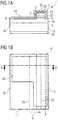
- FIG. 1B An example of a semiconductor laser is in a schematic plan view in FIG. 1B and in associated sectional view along the line AA 'in Figure 1A wherein the semiconductor laser is designed as an edge-emitting laser in ridge waveguide laser.
- the semiconductor laser 1 has a semiconductor body 2.
- the semiconductor body 2 comprises a semiconductor layer sequence with an active region 20 provided for generating radiation, a first semiconductor layer 21 and a second semiconductor layer 22.
- the semiconductor layer sequence forms the semiconductor body.
- the semiconductor body 2 is arranged on a carrier 5.
- the carrier 5 may, for example, be a growth substrate for the semiconductor layer sequence of the semiconductor body 2.
- a growth substrate based on gallium nitride in particular a substrate, in which regions of particularly low dislocation density are arranged between strip-shaped regions of higher dislocation density is suitable as the growth substrate.
- the support does not have to meet the high demands on the crystalline quality of a growth substrate, but rather can be selected in view of other properties such as thermal conductivity, thermal expansion or cost-effective availability.
- the carrier 5 can mechanically stabilize the semiconductor body 2, so that the growth substrate is no longer required and can thus be removed.
- the first semiconductor layer 21 and the second semiconductor layer 22 expediently have mutually different conductivity types.
- the first semiconductor layer may be p-type and the second semiconductor layer may be n-type, or vice versa.
- the first Semiconductor layer and the second semiconductor layer are preferably formed multi-layered.
- the first semiconductor layer and the second semiconductor layer may each have a waveguide layer on the side facing the active region 20, and a cladding layer on the side of the waveguide layer that faces away from the active region.
- the cladding layers expediently have a lower refractive index than the waveguide layers, so that the radiation generated in the active region 20 is guided within the waveguide layers.
- the cladding layers and the waveguide layers are not explicitly shown in the figures for the sake of simplicity.
- the semiconductor body 2 has a first side face 15 and a second side face 16, which bound the semiconductor body in the transverse direction. In the middle between these side surfaces runs a central axis 25 of the semiconductor body.
- the semiconductor body 2 has a radiation passage area 10 and a rear side 11 lying opposite the radiation passage area.
- the radiation passage area and the rear side form a resonator so that coherent radiation can be generated in the active area 20 during operation, the emission direction being perpendicular or substantially perpendicular to the radiation passage area.
- the radiation passage area and the rear side can be provided with a coating (not explicitly shown in the figures).
- the reflectivity is higher at the back than at the radiation passage area.
- the semiconductor body 2 has a web-shaped region 3 with a longitudinal axis 30 extending in the emission direction, wherein a rib waveguide is provided by means of the web-shaped region, which is provided for guiding the coherent radiation generated in the active region in the transverse direction.
- the longitudinal axis is offset relative to the central axis 25 of the semiconductor body 2, so that the central axis is arranged closer to the first side surface 15 than to the second side surface 16.
- An arrow 9 illustrates the course of a dislocation density gradient, wherein the dislocation density decreases in the direction of the arrow.
- the crystal quality of the semiconductor body is highest in the region that is critical to the generation of radiation in the operation of the semiconductor laser.
- the longitudinal axis of the web-shaped region is preferably offset by at least 10 ⁇ m, more preferably by at least 20 ⁇ m, for example by 30 ⁇ m or more, with respect to the central axis of the semiconductor body 2.
- the web-shaped region 3 has a comparatively high crystal quality.
- a contact layer 4 is formed on the semiconductor body 2.
- the contact layer 4 serves for external electrical contacting of the active region 2 from an upper side 35 of the web-shaped region 3, for example by means of a wire bond connection.
- a further contact layer 45 is formed, which is electrically conductively connected via the carrier 5 with the second semiconductor layer 22.
- an insulating layer 6 is arranged in regions between the contact layer 4 and the semiconductor body 2, which prevents an electrical short circuit of the active region.
- the insulation layer 6 On the upper side 35 of the web-shaped region 3, the insulation layer 6 has a recess 65 in which the contact layer 4 adjoins the first semiconductor layer 21 and establishes an electrically conductive connection to the semiconductor body from the upper side 35 of the web-shaped region.
- the contact layer 4 forms a contact surface 40, which is provided for external contacting by means of a bonding wire.
- the contact layer 4 and / or the further contact layer 45 preferably contain a metal, for example gold, nickel, titanium, platinum, rhodium, palladium, silver, aluminum or chromium or a metallic alloy with at least one of the metals mentioned.
- the contact layers may also be formed in multiple layers.
- the active region is based on a nitride compound semiconductor material and is suitable for generation in the ultraviolet, blue or green spectral range intended.
- a nitride compound semiconductor material is suitable for generation in the ultraviolet, blue or green spectral range intended.
- another semiconductor material in particular a III / V compound semiconductor material, such as InGaAlAs or InGaAlP, find application.
- the extent of the contact surface 40 in the transverse direction is preferably at least 0.3 times, more preferably at least 0.4 times, the extent of the semiconductor body 2. In this way, it is ensured that the semiconductor body protrudes from the side facing away from the carrier 5 simple manner is electrically contactable.
- the width of the contact surface in the transverse direction may have a width of 80 ⁇ m or more, for example 105 ⁇ m, for a width of the semiconductor body 2 of 200 ⁇ m.
- the wire bond connection would be too close to the web-shaped region and the web-shaped region would be damaged or even destroyed during the manufacture of the wire bond connection.
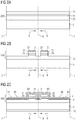
- An exemplary embodiment of a manufacturing method is based on shown in schematic sectional view intermediate steps in the FIGS. 2A and 2C and a supervision in FIG. 2D shown.
- a substrate which has a strip-shaped structuring.
- a distance between two adjacent, parallel mutually extending dividing lines 7 may be between 100 .mu.m and 600 .mu.m, preferably between 200 .mu.m and 500 .mu.m, for example 400 .mu.m.
- dividing lines 7 In order to simplify the illustration, only one area of the carrier 5 extending between two adjacent dividing lines 7 is shown in the figures.
- the dividing lines 7 On the surface of the carrier 5, the dividing lines 7 form a strip-shaped pattern, the defect density being higher along the dividing lines than between the dividing lines.
- a center line 8 is further shown for illustrative purposes, which runs parallel to them at half the distance between the dividing lines 7.
- the arrows 9 illustrate the gradient of the dislocation density, which increases from the center line 8 to the dividing lines 7, so that in the area around the center lines the crystal quality of the carrier is highest in each case.
- a semiconductor layer sequence 200 having an active region 20, a first semiconductor layer 21 and a second semiconductor layer 22 is deposited epitaxially, for example by means of MBE or MOCVD.
- the semiconductor layer sequence 200 is structured in such a way that ridge-shaped regions 3 are formed which, viewed from above the carrier, have a longitudinal axis 30 extending parallel to the separating lines 7 ( FIG. 2B ).
- the structuring can be carried out, for example, by wet-chemical or dry-chemical etching.
- the structuring takes place here in such a way that a first web-shaped region 31 and a second web-shaped region 32 are formed next to one another in the transverse direction between two adjacent separating lines 7.
- the web-shaped regions 31, 32 are each arranged closer to the center line 8 than at the respectively closest separating line 7. It can thus be achieved that both web-shaped regions are arranged close to the center line and thus can have a high crystalline quality.
- the semiconductor body 2 with the first web-shaped region 31 and the semiconductor body with the second web-shaped region 32 are formed axially symmetrically with respect to the center line.
- the web-shaped regions in the middle of the semiconductor bodies, that is to say without offset between the center axis of the semiconductor body and the longitudinal axis of the web-shaped region, the web-shaped regions would run closer to the separation lines and therefore have a reduced crystal quality.
- an insulating layer 6 is formed on the structured semiconductor layer sequence 200 formed, which has recesses 65 on an upper side of the web-shaped regions 31, 32.
- the insulation layer is particularly intended to protect the active region 20 from an electrical short circuit.
- a nitride such as silicon nitride
- an oxide such as titanium oxide or silicon oxide
- an oxynitride such as silicon oxynitride
- a contact layer 4 is deposited on the semiconductor layer sequence 200, which forms an electrical contact with the first semiconductor layer 21 in the region of the web-shaped regions 31, 32 through the recesses 65.
- first contact surface 41 or a second contact surface 42 which are provided for the external electrical contacting of the semiconductor laser.
- An extension of the contact surfaces in the transverse direction is preferably at least 20% of the distance between two adjacent parting lines.
- a further contact layer 45 is further deposited, which serves the underside external electrical contacting.
- the deposition of the contact layer 4 and / or the further contact layer 45 can be effected, for example, by means of sputtering or vapor deposition. Furthermore, the contact layer and / or the further contact layer can also be designed as a multilayer.
- a coating of the radiation passage area 10 and the back 11 can take place. This can in particular be carried out before the semiconductor bodies are separated along the dividing lines 7 and along the center lines 8.
- the carrier is split along the dividing line 7 and the center lines 8. After completion of the singulation, in each case the first side surfaces 15 of the semiconductor bodies 2 run along the center line 8 and the second side surfaces 16 run along the parting lines 7.
- This division can be effected in particular mechanically, for example by means of splitting, breaking, scratching or sawing, chemically, for example by wet-chemical or dry-chemical etching, and / or by means of coherent radiation, for example laser radiation.
- the semiconductor body with the first web-shaped region 31 and the semiconductor body with the second web-shaped region 32 differ in their basic shape in addition to the staggered arrangement of the web-shaped regions in that the contact surfaces 41 and 42, viewed in the direction of the radiation passage surface 10, are on different sides of the web-shaped area are arranged.
- the contact surface 42 has a marking 420, by means of which the semiconductor bodies 2 can be differentiated from one another in a simplified manner after the singulation, for example by means of an automatic optical recognition.
- a marking 420 by means of which the semiconductor bodies 2 can be differentiated from one another in a simplified manner after the singulation, for example by means of an automatic optical recognition.
- the marking is merely an example in the form of a region in which the size of the second contact surface 42 is reduced compared to the size of the first contact surface 41.
- another type of marking can also be formed, wherein the markings can also be formed as separate regions on the semiconductor body, which need not necessarily also serve for electrical contacting of the semiconductor body 2.
- the marking 420 may also be in the form of characters, such as numbers and / or letters, formed on the semiconductor body 2, which are spaced from the contact surfaces 40.
- a web-shaped region 3 has been shown by way of example, in which the active region 20 is formed in the web-shaped region. Deviating from the web-shaped region 3 may also be formed such that the active region 20 is not severed in the structuring, so that only the first semiconductor layer 21 forms the ridge-shaped region. In this case, the insulating layer 6 can also be dispensed with. Furthermore, it is also conceivable to form the web-shaped region outside the semiconductor body, for example in the form of a strip-shaped region of the contact layer 4.
- the semiconductor body 2 with the first web-shaped region 31 and the semiconductor body with the second web-shaped region 32 may also be formed point-symmetrical to each other of the described embodiment, in particular with a symmetry point on the center line 8. This can be achieved that when separating the carrier similar semiconductor lasers emerge.
- the radiation passage area of the semiconductor body with the first web-shaped area 31 and the radiation passage area of the semiconductor body with the second web-shaped area 32 are located on different sides before the singulation along the center line 8. Therefore, a coating of the radiation passage area 10 and the rear side 11 preferably takes place after the separation of the semiconductor bodies, so that the rear sides can each have a higher reflectivity than the radiation passage areas.
Landscapes
- Physics & Mathematics (AREA)
- Condensed Matter Physics & Semiconductors (AREA)
- General Physics & Mathematics (AREA)
- Electromagnetism (AREA)
- Optics & Photonics (AREA)
- Chemical & Material Sciences (AREA)
- Crystallography & Structural Chemistry (AREA)
- Geometry (AREA)
- Semiconductor Lasers (AREA)
Claims (7)
- Procédé de fabrication d'une pluralité de corps semi-conducteurs, comprenant les étapes :a) fourniture d'un support (5) doté d'une pluralité de zones de composants qui sont séparées les unes des autres par des lignes de séparation (7) ;b) dépôt d'une succession de couches semi-conductrices (200) comprenant une zone active (20) prévue pour générer un rayonnement ;c) réalisation, à partir de la succession de couches semi-conductrices, d'une pluralité de zones (3) en forme de nervure, de manière à ce qu'entre deux lignes de séparation voisines, exactement deux zones en forme de nervure soient réalisées l'une à côté de l'autre dans une direction s'étendant perpendiculairement aux lignes de séparation, les lignes de séparation s'étendant le long de zones du support dans lesquelles une densité de dislocation, comparée à des zones s'étendant entre les lignes de séparation, est plus élevée, et au moins une première zone (31) en forme de nervure ou une deuxième zone (32) en forme de nervure des zones en forme de nervure étant disposée de manière plus proche d'une ligne médiane (8) s'étendant entre les lignes de séparation voisines que de la ligne de séparation la plus proche de cette zone en forme de nervure, la densité de dislocation, en partant de la ligne médiane, augmentant en direction des lignes de séparation, et une couche de contact (4) étant réalisée sur la succession de couches semi-conductrices de manière à ce qu'une surface de contact (41, 42) prévue respectivement sur le côté détourné de la ligne médiane soit assignée aux zones en forme de nervure pour la mise en contact électrique externe de la zone active ; etd) individualisation de la succession de couches semi-conductrices le long des lignes de séparation et le long de la ligne médiane en une pluralité de corps semi-conducteurs (2) qui présentent respectivement au moins une zone en forme de nervure ;caractérisé en ce qu'
à l'étape c), un marquage (420) est réalisé au moyen de la surface de contact, à l'aide duquel le corps semi-conducteur ayant la première zone en forme de nervure et le corps semi-conducteur ayant la deuxième zone en forme de nervure peuvent être optiquement distingués l'un de l'autre. - Procédé selon la revendication 1,
dans lequel les deux zones en forme de nervure sont disposées plus près de la ligne médiane que de la ligne de séparation respectivement la plus proche. - Procédé selon la revendication 1 ou 2,
dans lequel la ligne médiane forme un axe de symétrie par rapport auquel le corps semi-conducteur ayant la première zone en forme de nervure et le corps semi-conducteur ayant la deuxième zone en forme de nervure sont en symétrie d'axe l'un par rapport à l'autre. - Procédé selon l'une quelconque des revendications 1 à 3, dans lequel le corps semi-conducteur ayant la première zone en forme de nervure et le corps semi-conducteur ayant la deuxième zone en forme de nervure sont distingués l'un de l'autre au moyen d'une identification optique automatique.
- Procédé selon l'une quelconque des revendications 1 à 4, dans lequel une étendue de la surface de contact est d'au moins 20% de l'écart entre deux lignes de séparation.
- Procédé selon l'une quelconque des revendications 1 à 5, dans lequel le support est à base de GaN.
- Procédé selon l'une quelconque des revendications 1 à 6, dans lequel une première surface de contact (41) est assignée au corps semi-conducteur ayant la première zone en forme de nervure et dans lequel une deuxième surface de contact (42) est assignée au corps semi-conducteur ayant la deuxième zone en forme de nervure, le marquage étant réalisé en tant qu'une zone dans laquelle la taille de la première surface de contact est réduite par rapport à la taille de la deuxième surface de contact.
Applications Claiming Priority (2)
| Application Number | Priority Date | Filing Date | Title |
|---|---|---|---|
| DE102009058345.9A DE102009058345B4 (de) | 2009-12-15 | 2009-12-15 | Halbleiterlaser |
| PCT/EP2010/067402 WO2011072964A1 (fr) | 2009-12-15 | 2010-11-12 | Laser à semi-conducteur |
Publications (2)
| Publication Number | Publication Date |
|---|---|
| EP2514049A1 EP2514049A1 (fr) | 2012-10-24 |
| EP2514049B1 true EP2514049B1 (fr) | 2018-08-08 |
Family
ID=43567921
Family Applications (1)
| Application Number | Title | Priority Date | Filing Date |
|---|---|---|---|
| EP10779771.4A Active EP2514049B1 (fr) | 2009-12-15 | 2010-11-12 | Procédé de fabrication d'éléments électroluminescents semi-conducteurs |
Country Status (8)
| Country | Link |
|---|---|
| US (1) | US8879596B2 (fr) |
| EP (1) | EP2514049B1 (fr) |
| JP (1) | JP5744054B2 (fr) |
| KR (1) | KR101723143B1 (fr) |
| CN (1) | CN102668277B (fr) |
| DE (1) | DE102009058345B4 (fr) |
| TW (1) | TWI438992B (fr) |
| WO (1) | WO2011072964A1 (fr) |
Families Citing this family (3)
| Publication number | Priority date | Publication date | Assignee | Title |
|---|---|---|---|---|
| DE102013107971A1 (de) * | 2013-07-25 | 2015-01-29 | Osram Opto Semiconductors Gmbh | Optoelektronischer Halbleiterchip, Halbleiterbauelement und Verfahren zur Herstellung von optoelektronischen Halbleiterchips |
| DE102013216527A1 (de) | 2013-08-21 | 2015-02-26 | Osram Opto Semiconductors Gmbh | Laserbauelement und Verfahren zum Herstellen eines Laserbauelements |
| DE102013220641A1 (de) | 2013-10-14 | 2015-04-16 | Osram Opto Semiconductors Gmbh | Halbleiterlaser mit einseitig verbreiterter Ridgestruktur |
Citations (3)
| Publication number | Priority date | Publication date | Assignee | Title |
|---|---|---|---|---|
| US20080130698A1 (en) * | 2006-11-30 | 2008-06-05 | Sanyo Electric Co., Ltd. | Nitride-based semiconductor device and method of fabricating the same |
| US20090185594A1 (en) * | 2008-01-21 | 2009-07-23 | Sanyo Electric Co., Ltd. | Semiconductor laser device and method of manufacturing the same |
| JP2009200341A (ja) * | 2008-02-22 | 2009-09-03 | Sharp Corp | 窒化物系半導体ウェハ、窒化物系半導体レーザ素子および窒化物系半導体レーザ素子の製造方法 |
Family Cites Families (15)
| Publication number | Priority date | Publication date | Assignee | Title |
|---|---|---|---|---|
| CA2044717A1 (fr) | 1990-06-18 | 1991-12-19 | Candadai S. Ramadoss | Procede de separation de proteines, de polypeptides ou de metaux |
| JPH0679172U (ja) * | 1993-04-14 | 1994-11-04 | 松下電器産業株式会社 | 半導体レーザ |
| EP0874405A3 (fr) | 1997-03-25 | 2004-09-15 | Mitsubishi Cable Industries, Ltd. | Element à base de GaN avec une faible densité de dislocations, son utilisation et procédés de fabrication |
| JPH11233877A (ja) * | 1998-02-16 | 1999-08-27 | Nec Corp | アレイ型レーザダイオード |
| WO2002065556A1 (fr) | 2001-02-15 | 2002-08-22 | Sharp Kabushiki Kaisha | Element de source lumineuse a semi-conducteur a base de nitrure et son procede de realisation |
| WO2003038957A1 (fr) | 2001-10-29 | 2003-05-08 | Sharp Kabushiki Kaisha | Dispositif a semi-conducteur au nitrure, son procede de fabrication et appareil optique a semi-conducteur |
| US6812496B2 (en) | 2002-01-10 | 2004-11-02 | Sharp Kabushiki Kaisha | Group III nitride semiconductor laser device |
| JP2003332676A (ja) | 2002-05-08 | 2003-11-21 | Mitsubishi Electric Corp | 半導体光装置 |
| JP2004095859A (ja) * | 2002-08-30 | 2004-03-25 | Sharp Corp | 半導体レーザ及びその製造方法 |
| US7372077B2 (en) * | 2003-02-07 | 2008-05-13 | Sanyo Electric Co., Ltd. | Semiconductor device |
| WO2006054543A1 (fr) * | 2004-11-22 | 2006-05-26 | Matsushita Electric Industrial Co., Ltd. | Dispositif semi-conducteur en composé de nitrure et procédé de fabrication idoine |
| JP4617907B2 (ja) * | 2005-02-03 | 2011-01-26 | ソニー株式会社 | 光集積型半導体発光素子 |
| JP2007173402A (ja) * | 2005-12-20 | 2007-07-05 | Matsushita Electric Ind Co Ltd | 半導体レーザ装置 |
| JPWO2008047751A1 (ja) * | 2006-10-17 | 2010-02-25 | 三洋電機株式会社 | 窒化物系半導体レーザ素子およびその製造方法 |
| JP2009088270A (ja) * | 2007-09-28 | 2009-04-23 | Sanyo Electric Co Ltd | 半導体素子の製造方法 |
-
2009
- 2009-12-15 DE DE102009058345.9A patent/DE102009058345B4/de active Active
-
2010
- 2010-11-12 KR KR1020127018374A patent/KR101723143B1/ko active IP Right Grant
- 2010-11-12 WO PCT/EP2010/067402 patent/WO2011072964A1/fr active Application Filing
- 2010-11-12 EP EP10779771.4A patent/EP2514049B1/fr active Active
- 2010-11-12 US US13/515,024 patent/US8879596B2/en active Active
- 2010-11-12 CN CN201080057349.9A patent/CN102668277B/zh active Active
- 2010-11-12 JP JP2012543557A patent/JP5744054B2/ja active Active
- 2010-12-10 TW TW099143215A patent/TWI438992B/zh active
Patent Citations (3)
| Publication number | Priority date | Publication date | Assignee | Title |
|---|---|---|---|---|
| US20080130698A1 (en) * | 2006-11-30 | 2008-06-05 | Sanyo Electric Co., Ltd. | Nitride-based semiconductor device and method of fabricating the same |
| US20090185594A1 (en) * | 2008-01-21 | 2009-07-23 | Sanyo Electric Co., Ltd. | Semiconductor laser device and method of manufacturing the same |
| JP2009200341A (ja) * | 2008-02-22 | 2009-09-03 | Sharp Corp | 窒化物系半導体ウェハ、窒化物系半導体レーザ素子および窒化物系半導体レーザ素子の製造方法 |
Also Published As
| Publication number | Publication date |
|---|---|
| EP2514049A1 (fr) | 2012-10-24 |
| TW201131918A (en) | 2011-09-16 |
| JP5744054B2 (ja) | 2015-07-01 |
| DE102009058345B4 (de) | 2021-05-12 |
| US8879596B2 (en) | 2014-11-04 |
| US20120287956A1 (en) | 2012-11-15 |
| KR101723143B1 (ko) | 2017-04-04 |
| TWI438992B (zh) | 2014-05-21 |
| CN102668277B (zh) | 2014-06-18 |
| JP2013513956A (ja) | 2013-04-22 |
| CN102668277A (zh) | 2012-09-12 |
| DE102009058345A1 (de) | 2011-06-16 |
| WO2011072964A1 (fr) | 2011-06-23 |
| KR20120112559A (ko) | 2012-10-11 |
Similar Documents
| Publication | Publication Date | Title |
|---|---|---|
| EP2260516B1 (fr) | Puce semiconductrice optoélectronique et procédé de fabrication associé | |
| DE102006046449B4 (de) | Verfahren zur Herstellung einer vertikal strukturierten Leuchtdiode | |
| DE102007032555A1 (de) | Halbleiterchip und Verfahren zur Herstellung eines Halbleiterchips | |
| DE102007029370A1 (de) | Halbleiterchip und Verfahren zur Herstellung eines Halbleiterchips | |
| DE102010034665A1 (de) | Optoelektronischer Halbleiterchip und Verfahren zur Herstellung von optoelektronischen Halbleiterchips | |
| DE102017130131B4 (de) | Verfahren zur Herstellung von optoelektronischen Halbleiterbauteilen und optoelektronisches Halbleiterbauteil | |
| EP2980864B1 (fr) | Puce semi-conductrice optoelectronique et procede de fabrication d'une puce semi-conductrice optoelectronique | |
| EP2415086B1 (fr) | Procédé de fabrication d'un composant optoélectronique, composant optoélectronique et ensemble comprenant plusieurs composants optoélectroniques | |
| WO2013083438A1 (fr) | Puce semiconductrice optoélectronique | |
| DE102015116970A1 (de) | Halbleiterlaser und Verfahren zur Herstellung eines Halbleiterlasers | |
| DE102010032497A1 (de) | Strahlungsemittierender Halbleiterchip und Verfahren zur Herstellung eines strahlungsemittierenden Halbleiterchips | |
| EP2569832A2 (fr) | Laser à semi-conducteurs à émission latérale | |
| EP2514049B1 (fr) | Procédé de fabrication d'éléments électroluminescents semi-conducteurs | |
| DE112018001450B4 (de) | Optoelektronischer Halbleiterchip und Verfahren zu dessen Herstellung | |
| DE102015111046A1 (de) | Optoelektronischer Halbleiterchip | |
| DE102017122325A1 (de) | Strahlungsemittierendes Halbleiterbauelement und Verfahren zur Herstellung von strahlungsemittierenden Halbleiterbauelementen | |
| DE102016124860A1 (de) | Optoelektronischer Halbleiterchip und Verfahren zur Herstellung eines optoelektronischen Halbleiterchips | |
| WO2015011028A1 (fr) | Puce semi-conductrice optoélectronique, composant à semi-conducteur et procédé permettant de produire des puces semi-conductrices optoélectroniques | |
| DE102008015253B4 (de) | Verfahren zur Herstellung eines Laserbauelements und Laserbauelement | |
| DE102019134756A1 (de) | Verfahren zur herstellung einer beleuchtungsvorrichtung | |
| DE102018123932A1 (de) | Optoelektronisches Bauelement mit dielektrischer Spiegelschicht und Verfahren zur Herstellung des optoelektronischen Bauelements | |
| DE10162914A1 (de) | Lichtemittierendes Halbleiterbauelement | |
| DE102016120685A1 (de) | Verfahren zur Herstellung eines Halbleiterlasers und Halbleiterlaser | |
| DE102015102458A1 (de) | Verfahren zur Herstellung einer Mehrzahl von Halbleiterchips und Halbleiterchip | |
| DE102022115644A1 (de) | Laserdiodenbauelement und verfahren zur herstellung zumindest eines laserdiodenbauelements |
Legal Events
| Date | Code | Title | Description |
|---|---|---|---|
| PUAI | Public reference made under article 153(3) epc to a published international application that has entered the european phase |
Free format text: ORIGINAL CODE: 0009012 |
|
| 17P | Request for examination filed |
Effective date: 20120703 |
|
| AK | Designated contracting states |
Kind code of ref document: A1 Designated state(s): AL AT BE BG CH CY CZ DE DK EE ES FI FR GB GR HR HU IE IS IT LI LT LU LV MC MK MT NL NO PL PT RO RS SE SI SK SM TR |
|
| RIN1 | Information on inventor provided before grant (corrected) |
Inventor name: DINI, DIMITRI Inventor name: SCHILLGALIES, MARC |
|
| DAX | Request for extension of the european patent (deleted) | ||
| 17Q | First examination report despatched |
Effective date: 20140801 |
|
| GRAP | Despatch of communication of intention to grant a patent |
Free format text: ORIGINAL CODE: EPIDOSNIGR1 |
|
| RIC1 | Information provided on ipc code assigned before grant |
Ipc: H01S 5/22 20060101ALI20180308BHEP Ipc: H01L 33/32 20100101ALI20180308BHEP Ipc: H01S 5/02 20060101AFI20180308BHEP Ipc: H01S 5/323 20060101ALI20180308BHEP Ipc: H01S 5/042 20060101ALI20180308BHEP Ipc: H01L 33/16 20100101ALI20180308BHEP |
|
| INTG | Intention to grant announced |
Effective date: 20180405 |
|
| GRAS | Grant fee paid |
Free format text: ORIGINAL CODE: EPIDOSNIGR3 |
|
| GRAA | (expected) grant |
Free format text: ORIGINAL CODE: 0009210 |
|
| AK | Designated contracting states |
Kind code of ref document: B1 Designated state(s): AL AT BE BG CH CY CZ DE DK EE ES FI FR GB GR HR HU IE IS IT LI LT LU LV MC MK MT NL NO PL PT RO RS SE SI SK SM TR |
|
| REG | Reference to a national code |
Ref country code: GB Ref legal event code: FG4D Free format text: NOT ENGLISH |
|
| REG | Reference to a national code |
Ref country code: CH Ref legal event code: EP Ref country code: AT Ref legal event code: REF Ref document number: 1028077 Country of ref document: AT Kind code of ref document: T Effective date: 20180815 |
|
| REG | Reference to a national code |
Ref country code: IE Ref legal event code: FG4D Free format text: LANGUAGE OF EP DOCUMENT: GERMAN |
|
| REG | Reference to a national code |
Ref country code: DE Ref legal event code: R096 Ref document number: 502010015252 Country of ref document: DE |
|
| REG | Reference to a national code |
Ref country code: NL Ref legal event code: MP Effective date: 20180808 |
|
| REG | Reference to a national code |
Ref country code: LT Ref legal event code: MG4D |
|
| PG25 | Lapsed in a contracting state [announced via postgrant information from national office to epo] |
Ref country code: SE Free format text: LAPSE BECAUSE OF FAILURE TO SUBMIT A TRANSLATION OF THE DESCRIPTION OR TO PAY THE FEE WITHIN THE PRESCRIBED TIME-LIMIT Effective date: 20180808 Ref country code: BG Free format text: LAPSE BECAUSE OF FAILURE TO SUBMIT A TRANSLATION OF THE DESCRIPTION OR TO PAY THE FEE WITHIN THE PRESCRIBED TIME-LIMIT Effective date: 20181108 Ref country code: GR Free format text: LAPSE BECAUSE OF FAILURE TO SUBMIT A TRANSLATION OF THE DESCRIPTION OR TO PAY THE FEE WITHIN THE PRESCRIBED TIME-LIMIT Effective date: 20181109 Ref country code: NL Free format text: LAPSE BECAUSE OF FAILURE TO SUBMIT A TRANSLATION OF THE DESCRIPTION OR TO PAY THE FEE WITHIN THE PRESCRIBED TIME-LIMIT Effective date: 20180808 Ref country code: LT Free format text: LAPSE BECAUSE OF FAILURE TO SUBMIT A TRANSLATION OF THE DESCRIPTION OR TO PAY THE FEE WITHIN THE PRESCRIBED TIME-LIMIT Effective date: 20180808 Ref country code: PL Free format text: LAPSE BECAUSE OF FAILURE TO SUBMIT A TRANSLATION OF THE DESCRIPTION OR TO PAY THE FEE WITHIN THE PRESCRIBED TIME-LIMIT Effective date: 20180808 Ref country code: FI Free format text: LAPSE BECAUSE OF FAILURE TO SUBMIT A TRANSLATION OF THE DESCRIPTION OR TO PAY THE FEE WITHIN THE PRESCRIBED TIME-LIMIT Effective date: 20180808 Ref country code: RS Free format text: LAPSE BECAUSE OF FAILURE TO SUBMIT A TRANSLATION OF THE DESCRIPTION OR TO PAY THE FEE WITHIN THE PRESCRIBED TIME-LIMIT Effective date: 20180808 Ref country code: IS Free format text: LAPSE BECAUSE OF FAILURE TO SUBMIT A TRANSLATION OF THE DESCRIPTION OR TO PAY THE FEE WITHIN THE PRESCRIBED TIME-LIMIT Effective date: 20181208 Ref country code: NO Free format text: LAPSE BECAUSE OF FAILURE TO SUBMIT A TRANSLATION OF THE DESCRIPTION OR TO PAY THE FEE WITHIN THE PRESCRIBED TIME-LIMIT Effective date: 20181108 |
|
| PG25 | Lapsed in a contracting state [announced via postgrant information from national office to epo] |
Ref country code: LV Free format text: LAPSE BECAUSE OF FAILURE TO SUBMIT A TRANSLATION OF THE DESCRIPTION OR TO PAY THE FEE WITHIN THE PRESCRIBED TIME-LIMIT Effective date: 20180808 Ref country code: HR Free format text: LAPSE BECAUSE OF FAILURE TO SUBMIT A TRANSLATION OF THE DESCRIPTION OR TO PAY THE FEE WITHIN THE PRESCRIBED TIME-LIMIT Effective date: 20180808 Ref country code: AL Free format text: LAPSE BECAUSE OF FAILURE TO SUBMIT A TRANSLATION OF THE DESCRIPTION OR TO PAY THE FEE WITHIN THE PRESCRIBED TIME-LIMIT Effective date: 20180808 |
|
| PG25 | Lapsed in a contracting state [announced via postgrant information from national office to epo] |
Ref country code: RO Free format text: LAPSE BECAUSE OF FAILURE TO SUBMIT A TRANSLATION OF THE DESCRIPTION OR TO PAY THE FEE WITHIN THE PRESCRIBED TIME-LIMIT Effective date: 20180808 Ref country code: CZ Free format text: LAPSE BECAUSE OF FAILURE TO SUBMIT A TRANSLATION OF THE DESCRIPTION OR TO PAY THE FEE WITHIN THE PRESCRIBED TIME-LIMIT Effective date: 20180808 Ref country code: IT Free format text: LAPSE BECAUSE OF FAILURE TO SUBMIT A TRANSLATION OF THE DESCRIPTION OR TO PAY THE FEE WITHIN THE PRESCRIBED TIME-LIMIT Effective date: 20180808 Ref country code: EE Free format text: LAPSE BECAUSE OF FAILURE TO SUBMIT A TRANSLATION OF THE DESCRIPTION OR TO PAY THE FEE WITHIN THE PRESCRIBED TIME-LIMIT Effective date: 20180808 Ref country code: ES Free format text: LAPSE BECAUSE OF FAILURE TO SUBMIT A TRANSLATION OF THE DESCRIPTION OR TO PAY THE FEE WITHIN THE PRESCRIBED TIME-LIMIT Effective date: 20180808 |
|
| REG | Reference to a national code |
Ref country code: DE Ref legal event code: R097 Ref document number: 502010015252 Country of ref document: DE |
|
| PG25 | Lapsed in a contracting state [announced via postgrant information from national office to epo] |
Ref country code: SK Free format text: LAPSE BECAUSE OF FAILURE TO SUBMIT A TRANSLATION OF THE DESCRIPTION OR TO PAY THE FEE WITHIN THE PRESCRIBED TIME-LIMIT Effective date: 20180808 Ref country code: DK Free format text: LAPSE BECAUSE OF FAILURE TO SUBMIT A TRANSLATION OF THE DESCRIPTION OR TO PAY THE FEE WITHIN THE PRESCRIBED TIME-LIMIT Effective date: 20180808 Ref country code: SM Free format text: LAPSE BECAUSE OF FAILURE TO SUBMIT A TRANSLATION OF THE DESCRIPTION OR TO PAY THE FEE WITHIN THE PRESCRIBED TIME-LIMIT Effective date: 20180808 |
|
| PLBE | No opposition filed within time limit |
Free format text: ORIGINAL CODE: 0009261 |
|
| STAA | Information on the status of an ep patent application or granted ep patent |
Free format text: STATUS: NO OPPOSITION FILED WITHIN TIME LIMIT |
|
| REG | Reference to a national code |
Ref country code: CH Ref legal event code: PL |
|
| 26N | No opposition filed |
Effective date: 20190509 |
|
| GBPC | Gb: european patent ceased through non-payment of renewal fee |
Effective date: 20181112 |
|
| PG25 | Lapsed in a contracting state [announced via postgrant information from national office to epo] |
Ref country code: MC Free format text: LAPSE BECAUSE OF FAILURE TO SUBMIT A TRANSLATION OF THE DESCRIPTION OR TO PAY THE FEE WITHIN THE PRESCRIBED TIME-LIMIT Effective date: 20180808 Ref country code: LU Free format text: LAPSE BECAUSE OF NON-PAYMENT OF DUE FEES Effective date: 20181112 |
|
| REG | Reference to a national code |
Ref country code: BE Ref legal event code: MM Effective date: 20181130 |
|
| REG | Reference to a national code |
Ref country code: IE Ref legal event code: MM4A |
|
| PG25 | Lapsed in a contracting state [announced via postgrant information from national office to epo] |
Ref country code: CH Free format text: LAPSE BECAUSE OF NON-PAYMENT OF DUE FEES Effective date: 20181130 Ref country code: LI Free format text: LAPSE BECAUSE OF NON-PAYMENT OF DUE FEES Effective date: 20181130 Ref country code: SI Free format text: LAPSE BECAUSE OF FAILURE TO SUBMIT A TRANSLATION OF THE DESCRIPTION OR TO PAY THE FEE WITHIN THE PRESCRIBED TIME-LIMIT Effective date: 20180808 |
|
| PG25 | Lapsed in a contracting state [announced via postgrant information from national office to epo] |
Ref country code: IE Free format text: LAPSE BECAUSE OF NON-PAYMENT OF DUE FEES Effective date: 20181112 Ref country code: FR Free format text: LAPSE BECAUSE OF NON-PAYMENT OF DUE FEES Effective date: 20181130 |
|
| PG25 | Lapsed in a contracting state [announced via postgrant information from national office to epo] |
Ref country code: BE Free format text: LAPSE BECAUSE OF NON-PAYMENT OF DUE FEES Effective date: 20181130 |
|
| PG25 | Lapsed in a contracting state [announced via postgrant information from national office to epo] |
Ref country code: GB Free format text: LAPSE BECAUSE OF NON-PAYMENT OF DUE FEES Effective date: 20181112 |
|
| REG | Reference to a national code |
Ref country code: AT Ref legal event code: MM01 Ref document number: 1028077 Country of ref document: AT Kind code of ref document: T Effective date: 20181112 |
|
| PG25 | Lapsed in a contracting state [announced via postgrant information from national office to epo] |
Ref country code: AT Free format text: LAPSE BECAUSE OF NON-PAYMENT OF DUE FEES Effective date: 20181112 Ref country code: MT Free format text: LAPSE BECAUSE OF FAILURE TO SUBMIT A TRANSLATION OF THE DESCRIPTION OR TO PAY THE FEE WITHIN THE PRESCRIBED TIME-LIMIT Effective date: 20180808 |
|
| PG25 | Lapsed in a contracting state [announced via postgrant information from national office to epo] |
Ref country code: TR Free format text: LAPSE BECAUSE OF FAILURE TO SUBMIT A TRANSLATION OF THE DESCRIPTION OR TO PAY THE FEE WITHIN THE PRESCRIBED TIME-LIMIT Effective date: 20180808 |
|
| PG25 | Lapsed in a contracting state [announced via postgrant information from national office to epo] |
Ref country code: PT Free format text: LAPSE BECAUSE OF FAILURE TO SUBMIT A TRANSLATION OF THE DESCRIPTION OR TO PAY THE FEE WITHIN THE PRESCRIBED TIME-LIMIT Effective date: 20180808 |
|
| PG25 | Lapsed in a contracting state [announced via postgrant information from national office to epo] |
Ref country code: MK Free format text: LAPSE BECAUSE OF NON-PAYMENT OF DUE FEES Effective date: 20180808 Ref country code: HU Free format text: LAPSE BECAUSE OF FAILURE TO SUBMIT A TRANSLATION OF THE DESCRIPTION OR TO PAY THE FEE WITHIN THE PRESCRIBED TIME-LIMIT; INVALID AB INITIO Effective date: 20101112 Ref country code: CY Free format text: LAPSE BECAUSE OF FAILURE TO SUBMIT A TRANSLATION OF THE DESCRIPTION OR TO PAY THE FEE WITHIN THE PRESCRIBED TIME-LIMIT Effective date: 20180808 |
|
| P01 | Opt-out of the competence of the unified patent court (upc) registered |
Effective date: 20230825 |
|
| PGFP | Annual fee paid to national office [announced via postgrant information from national office to epo] |
Ref country code: DE Payment date: 20231121 Year of fee payment: 14 |