EP2507608B1 - Sensor mit einem sensorgehäuse - Google Patents
Sensor mit einem sensorgehäuse Download PDFInfo
- Publication number
- EP2507608B1 EP2507608B1 EP10775730.4A EP10775730A EP2507608B1 EP 2507608 B1 EP2507608 B1 EP 2507608B1 EP 10775730 A EP10775730 A EP 10775730A EP 2507608 B1 EP2507608 B1 EP 2507608B1
- Authority
- EP
- European Patent Office
- Prior art keywords
- metallization
- adhesive
- sensor
- base plate
- conductor track
- Prior art date
- Legal status (The legal status is an assumption and is not a legal conclusion. Google has not performed a legal analysis and makes no representation as to the accuracy of the status listed.)
- Active
Links
Images

Classifications
-
- H—ELECTRICITY
- H05—ELECTRIC TECHNIQUES NOT OTHERWISE PROVIDED FOR
- H05K—PRINTED CIRCUITS; CASINGS OR CONSTRUCTIONAL DETAILS OF ELECTRIC APPARATUS; MANUFACTURE OF ASSEMBLAGES OF ELECTRICAL COMPONENTS
- H05K7/00—Constructional details common to different types of electric apparatus
- H05K7/02—Arrangements of circuit components or wiring on supporting structure
-
- G—PHYSICS
- G01—MEASURING; TESTING
- G01L—MEASURING FORCE, STRESS, TORQUE, WORK, MECHANICAL POWER, MECHANICAL EFFICIENCY, OR FLUID PRESSURE
- G01L19/00—Details of, or accessories for, apparatus for measuring steady or quasi-steady pressure of a fluent medium insofar as such details or accessories are not special to particular types of pressure gauges
- G01L19/14—Housings
-
- G—PHYSICS
- G01—MEASURING; TESTING
- G01L—MEASURING FORCE, STRESS, TORQUE, WORK, MECHANICAL POWER, MECHANICAL EFFICIENCY, OR FLUID PRESSURE
- G01L19/00—Details of, or accessories for, apparatus for measuring steady or quasi-steady pressure of a fluent medium insofar as such details or accessories are not special to particular types of pressure gauges
- G01L19/14—Housings
- G01L19/148—Details about the circuit board integration, e.g. integrated with the diaphragm surface or encapsulation
-
- H—ELECTRICITY
- H05—ELECTRIC TECHNIQUES NOT OTHERWISE PROVIDED FOR
- H05K—PRINTED CIRCUITS; CASINGS OR CONSTRUCTIONAL DETAILS OF ELECTRIC APPARATUS; MANUFACTURE OF ASSEMBLAGES OF ELECTRICAL COMPONENTS
- H05K13/00—Apparatus or processes specially adapted for manufacturing or adjusting assemblages of electric components
-
- H—ELECTRICITY
- H10—SEMICONDUCTOR DEVICES; ELECTRIC SOLID-STATE DEVICES NOT OTHERWISE PROVIDED FOR
- H10W—GENERIC PACKAGES, INTERCONNECTIONS, CONNECTORS OR OTHER CONSTRUCTIONAL DETAILS OF DEVICES COVERED BY CLASS H10
- H10W72/00—Interconnections or connectors in packages
- H10W72/50—Bond wires
- H10W72/531—Shapes of wire connectors
- H10W72/5363—Shapes of wire connectors the connected ends being wedge-shaped
-
- H—ELECTRICITY
- H10—SEMICONDUCTOR DEVICES; ELECTRIC SOLID-STATE DEVICES NOT OTHERWISE PROVIDED FOR
- H10W—GENERIC PACKAGES, INTERCONNECTIONS, CONNECTORS OR OTHER CONSTRUCTIONAL DETAILS OF DEVICES COVERED BY CLASS H10
- H10W72/00—Interconnections or connectors in packages
- H10W72/50—Bond wires
- H10W72/541—Dispositions of bond wires
- H10W72/5445—Dispositions of bond wires being orthogonal to a side surface of the chip, e.g. parallel arrangements
-
- H—ELECTRICITY
- H10—SEMICONDUCTOR DEVICES; ELECTRIC SOLID-STATE DEVICES NOT OTHERWISE PROVIDED FOR
- H10W—GENERIC PACKAGES, INTERCONNECTIONS, CONNECTORS OR OTHER CONSTRUCTIONAL DETAILS OF DEVICES COVERED BY CLASS H10
- H10W90/00—Package configurations
- H10W90/701—Package configurations characterised by the relative positions of pads or connectors relative to package parts
- H10W90/751—Package configurations characterised by the relative positions of pads or connectors relative to package parts of bond wires
- H10W90/754—Package configurations characterised by the relative positions of pads or connectors relative to package parts of bond wires between a chip and a stacked insulating package substrate, interposer or RDL
-
- Y—GENERAL TAGGING OF NEW TECHNOLOGICAL DEVELOPMENTS; GENERAL TAGGING OF CROSS-SECTIONAL TECHNOLOGIES SPANNING OVER SEVERAL SECTIONS OF THE IPC; TECHNICAL SUBJECTS COVERED BY FORMER USPC CROSS-REFERENCE ART COLLECTIONS [XRACs] AND DIGESTS
- Y10—TECHNICAL SUBJECTS COVERED BY FORMER USPC
- Y10T—TECHNICAL SUBJECTS COVERED BY FORMER US CLASSIFICATION
- Y10T29/00—Metal working
- Y10T29/49—Method of mechanical manufacture
- Y10T29/49002—Electrical device making
Definitions
- the DE 102 23 357 A1 refers to a device for pressure measurement.
- the device for pressure measurement comprises a housing in which a carrier provided with a sensor element and with electrical connection elements is arranged.
- the housing has a first housing space surrounding the sensor element and connected in a first pressure channel of a first pressure connection, and a second housing space sealed with respect to the first housing space and surrounding at least the electrical connection elements.
- the housing has a third housing space which is sealed off from the first housing space and the second housing space and which is connected to a second pressure channel of a second pressure port.
- CiH chip-in-housing
- the sensor chips are glued directly into the sensor housing made of plastic. If two chips, for example a sensor element and a separate electronic component such as an ASIC, are used, it is necessary to provide a plurality of electrical connections between the sensor element and the electrical component, such as the ASIC mentioned above.
- the design concept provides for the electronic component and the sensor element to be arranged in separate chambers. The separation between the two chambers must be designed media-tight against exhaust gas, moisture and other media.
- an injected into the housing of the pressure sensor leadframe is used, which is glued from both sides, in particular bonded.
- This technique sets a tight encapsulation of a Lead comb, ie the leadframe ahead, to prevent penetration, for example, of moisture.
- the required media tightness of inserts is usually not given.
- an attack on a gold or gold-plated surface of the conductor comb can occur, which promotes the formation of corrosion phenomena.
- the chamber in which the sensor element is received filled with a gel.
- the electronic component ASIC and the sensor element are also within one and the same housing area, or within one and the same chamber. It is also common for the sensor element and the electronic component, i. H. the ASIC are formed within one and the same silicon chip.
- An essential requirement for new generations of sensors, in particular of pressure sensors, is that they must be substantially more resistant to exhaust gas than previous sensor generations. It has been found that the exhaust gas resistance of the sensor element is easier to ensure than the exhaust gas resistance of the electronic component, for example an ASIC. This is in addition to a required variant management in terms of flexible compilation of customized sensor element characteristics with variable ASIC versions also the reason that the electronic component, in particular an ASIC and the sensor are to be separated from each other.
- the sensor element thus sits in a chamber that is exposed to the medium, in particular the exhaust gas, while the electronic component, d. H. the ASIC is located in a separate compartment which may not be exposed to the media.
- Low pressure sensors use two silicon chips. One of the two chips serves as a sensor element while the other serves as an electronic device, for example an ASIC.
- JP 11 326087 A and WO 03/1300371 A1 describe pressure sensors known from the prior art with a sensor housing and a sensor element.
- an electronic component for example an ASIC or a sensor element
- a base plate of a sensor housing which is produced in particular from plastic.
- the electronic component and the sensor element are preferably glued to an upper, the medium exposed, plan side of the base plate.
- an electrical connection is arranged, for example, a conductor.
- This electrical connection which serves as a conductor, is preferably shown in MID technology and may, for example, be represented as a metallization comprising a gold layer covering a base layer, for example a sub-nickel.
- the metallizations generated by the MID technology are preferably introduced into recesses in the plane surface of the base plate of the sensor housing.
- MID Molded Interconnect Devices
- conductive patterns in the form of a structured metal layer are applied to three-dimensional injection molded circuit boards.
- the MID technology combines mechanical and electrical functions in the component, as well as the combination of housing and circuit carrier function and the integration of mechanical connecting and fixing elements and snap hooks. This results in a significant reduction in the use of materials and the number of items. Furthermore, the assembly costs for the various components can be significantly reduced and shorten the process chain.
- the individual recesses for the individual strip-shaped metallizations are separated from one another by webs of the plastic material of the base plate.
- the metallizations can also be embedded by recesses, Einschallen or encapsulation of the plastic material in recesses with respect to the flat surface of the base plate.
- the metallizations serving as conductor tracks are preferably introduced into recesses with respect to the upper planar surface of the baseplate so that the recesses have a width which exceeds the stripe width of the metallizations, which are preferably pronounced in MID technology.
- a bond which comprises a bonding wire.
- One bonding point is located on the sensor element and another at one end of the metallization serving as a conductor track.
- the respective other end of the metallization serving as a conductor has a bonding point, from which extends a further bonding wire to the electronic component, for example to the ASIC.
- the adhesive material in the form of a bead of adhesive can be produced before or after the bonding connections are produced between the ends of the metallization serving as conductor track and the bonding wires to the electronic component or to the sensor element.
- the preferably applied in the form of a bead of adhesive on the serving as a conductor metallization adhesive material is placed between the two bonding sites that they are certainly not touched. This results in that the bonding points are not mechanically stressed and therefore results in a very robust construction of an electrical connection.
- the proposed solution according to the invention takes into account the fact that when a deterioration of the connection between serving as a conductor metallization and made of plastic material base plate, a medium can penetrate and thus a seal between the sensor element on the one hand and the electronic component, such as a ASIC, on the other hand is no longer given.
- the metallization serving as a conductor track is slightly raised within the depressions in the base plate, so that the adhesive material, in particular applied as a bead of adhesive, laterally closes between the ends of the metallizations serving as a conductor track and also seals off laterally between the metallizations Track metallizations and the material of the base plate results.
- the bonding sites at the ends of serving as a conductor metallization and the bonding wires themselves can be applied to the medium acted side of the base plate preferably made of plastic material, which covers both the individual bonding wires and the bonding positions.
- the preferably applied in the form of a Kleberaupe on serving as a conductor metallization adhesive material is media-tight and also seals the base plate and cover plate when joining against each other, so that no medium from the forming during the joining of cover member and base plate chamber for receiving the sensor element to the chamber, in which the electronic component, for example an ASIC, overflows.
- the flexibility of the adhesive material of the adhesive bead compensates in a particularly advantageous manner measure and installation tolerances.
- a sealing bar is arranged on the underside of the cover element to be applied to the base plate, which dips in preferably formed as Kleberaupe accumulations of adhesive material and finally the media-tight seal between the chamber in which the sensor element is received and the chamber in which the electronic component (ASIC ).
- the sealing blade moves on the underside of the cover element in the still soft and deformable material of the adhesive and deforms this, pushes this particular in the spaces between those serving as a conductor metallizations and the webs of the material of the base plate, so that a media-tight seal is formed.
- the dimensions of the sealing blade on the underside of the cover element are preferably selected so that it penetrates far enough into the bead of adhesive that a largely deformation of the material of the adhesive bead is carried out and sealing between the two chambers within the sensor housing can be achieved.
- the inventively proposed solution provides a particularly simple and short electrical connection between a sensor element and an electronic component such as an ASIC.
- the simple and short electrical connection offers advantages in terms of electromagnetic compatibility, space requirements and costs.
- the solution proposed according to the invention in media-tight connections between electronic components and the sensor element, a high exhaust resistance of the thereof formed entire sensor can be achieved.
- a mechanically robust design by at least two bond connections, which lead to a, representing a conductor, metallization. The sealing, via the adhesive bead takes place in particular outside the areas of the bonding sites, so that they are not mechanically stressed.
- FIG. 1 is to remove a base plate of a sensor housing, which comprises a sensor element and an electronic component, such as an ASIC.
- a sensor 10 shown only schematically it is for example a low pressure sensor, wherein on a common base plate 14, both an electronic component 16, for example, an ASIC as well as an exposed medium Sensor element 18 are arranged.
- the electronic component 16 and the sensor element 18 are glued to a plane surface 60 of the base plate 14 of the sensor housing 12.
- the electronic component 16 which may be, for example, an ASIC, as well as the sensor element 18 via individual bonding wires 26 connected to each other.
- the bonding wires 24 contact the opposite ends of a conductor 20, which may be given by a metallization 22, for example.
- the adhesive bead 28 can - as in FIG. 1 shown - a transverse to the longitudinal extent of the base plate 14 extending groove, in which, which will be described in more detail later, a sealing sword 50 of a cover member 44 dive.
- FIG. 2 shows that both the first bonding site 32 at one end of the conductive metallization 22, and the bonding wires 26 extending to the sensor element 18 may be covered by a gel 42.
- the gel 42 By means of the gel 42, both the bonding wires 26 and the first bonding point 32 are protected on the medium acted upon side 40 of the base plate 40 against the medium which is placed on the sensor element 18.
- the base plate 14 of the sensor housing 12 is made of a plastic material such as PPS, polyphenylene sulfide, a thermoplastic or PPA, polyphthalamide, also a thermoplastic manufactured.
- a manufacturing process offers the plastic injection molding process.
- FIG. 3 shows a section through the base plate in the region of the preferably applied as adhesive bead adhesive material.
- FIG. 3 As can be seen, the base plate 14 in the area which is covered by the adhesive bead 28 of the adhesive material, free spaces 36.
- the free spaces 36 are separated from each other by webs 56 of the material of the base plate 14.
- a web height of the material webs 56 of the material of the base plate 14 is indicated by reference numeral 58.
- the metallization 22 serving as conductor track 20 can be applied, for example, by hot stamping, insonification or by injection-molding of the plastic material.
- the metallizations 22 are preferably produced by means of the MID technique and have a layer structure which may comprise on the upper side, for example, an Au layer which is applied to a nickel layer.
- the adhesive bead 28 of the adhesive material extends between the ends of the individual metallizations 22 serving as a conductor track 20.
- the material of the adhesive bead 22 flows into the free spaces 36, so that serving as a conductor 20 metallizations 22 also laterally d. H. on their flanks, cf. Position 38, are enclosed by the adhesive material of the adhesive bead 28 and consequently a media-tight connection 62, formed by the flowing adhesive material of the adhesive bead 28, adjusts. This creates the seal between a region of the sensor housing 12 in which the sensor element 18 is accommodated and the remaining region of the sensor housing 12 in which the electronic component 16, designed as an ASIC, is located.
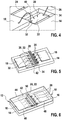
- the representation according to FIG. 4 is to be taken on an enlarged scale serving as a conductor metallization.
- the exposed from the medium sensor element 18 of the bonding wire 26 extends to one end of the acting as a conductor 20 metallization 22, and is electrically contacted at this end at a first bonding point 32 with the serving as a conductor 20 metallization 22.
- a second bonding point 34 At the opposite end of serving as a conductor 20 metallization 22 is a second bonding point 34, from which a further bonding wire 26 to the in FIG. 4 not shown electronic component 16, for example, an ASIC extends. From the illustration according to FIG. 4 shows that the bonding sites 32 and 34 between the bonding wires 26 and serving as a conductor metallization 22 are far apart that between the bonding sites 32 and 34 sufficient space for application of the adhesive brow 28 remains.
- Reference numeral 40 designates the medium-exposed side of the base plate 14 of the sensor housing 12.
- FIG. 5 shows a complete representation of the base plate 14, wherein on this one hand, the electronic component 16 and on the other hand, the sensor element 18 are added.
- the individual bonding wires 26, which connect the electronic component 16 to the sensor element 18, are covered by the adhesive bead 28, as are the bonding points 32, 34, which are located on the metallization 22 of the conductor tracks 20, which are in recesses on the upper side of the base plate 14 are admitted.
- Reference numeral 42 denotes a gel, which covers one half of the bonding wires 26, which extend from the second bonding points 32 to the sensor element 18.
- FIG. 6 shows the sensor housing, in which the cover element is joined to the base plate 14.
- FIG. 6 The representation according to FIG. 6 can be seen that in the assembled state of a cover member 44 with the base plate 14, a sealing blade 50 dips into the plastically deformable material of the adhesive bead 28 of the adhesive material.
- the sealing blade When the sealing blade is immersed on the underside of the cover element 44, the material of the adhesive bead 28 is deformed in such a way that it is moved into the free spaces 36, 38 (see FIG FIG. 3 ) flows and penetrates and consequently below the adhesive bead 28, a media-tight connection 62 is formed.
- This media-tight connection forms centrally on the plane surface 60 of the base plate 14 a chamber 46 in which the sensor element 18 is received by a further chamber 48 in which the electronic component 16, for example formed as ASIC, is located.
- the media-tight connection 62 is created by filling the elastically deformable material when the sealing blade 50 is immersed in the adhesive bead 28 and the free spaces 36 next to the metallizations 22 serving as the conductor track 20.
- both the bonding wires 26 and the first bonding points 32 which lie within the chamber 46, in which the sensor element 18 is received, be protected by a gel 42. Due to the media-tight connection 62 as shown in FIG FIG. 3 the overflow of the medium is prevented in the chamber 48, in which the sensitive electronic component 16 is arranged. Due to the elasticity of the adhesive material of the adhesive bead 28, which extends substantially transversely to the longitudinal extent of the base plate 14 of the sensor housing 12, a balance of dimension and installation tolerances of the sensor housing 12 of the sensor 10 is also achieved. The dimensions of the sealing blade 50 on the underside of the cover element 44 are preferably dimensioned such that it penetrates far into the adhesive material of the adhesive bead 28, that an optimal flow of the elastic deformable adhesive material of the adhesive bead 28 is achieved.
- a simple and short electrical connection 24 between the sensor element 18 and an electronic component 16 is achieved.
- the shortness of the electrical connection offers advantages in terms of electromagnetic compatibility and the space required in terms of manufacturing costs.
- a media-tight connection 62 is achieved within a sensor housing 12, which supports the CiH concept (chip-in-Housing), since during the preparation of the electrical connection, a seal between the chamber 46 for receiving the medium exposed sensor element 18 on the one hand and the chamber 48, in which the much more sensitive electronic component 16 is received, can be achieved. This results in an increased exhaust gas resistance of the sensor 10 with respect to the medium, in particular the exhaust gas.
- the proposed solution according to the invention is finally characterized by its mechanically robust design by only two bonds at the bonding points 32 and 34, which are guided on a serving as a conductor 20 metallization 22. Furthermore, the sealing via the adhesive material of the adhesive bead 28 takes place outside of the areas on which the bonding points 32, 34 lie, namely at the ends of the strip-shaped metallizations 22, which function as conductor track 22.
Landscapes
- Physics & Mathematics (AREA)
- General Physics & Mathematics (AREA)
- Engineering & Computer Science (AREA)
- Microelectronics & Electronic Packaging (AREA)
- Manufacturing & Machinery (AREA)
- Measuring Fluid Pressure (AREA)
- Pressure Sensors (AREA)
- Testing Or Calibration Of Command Recording Devices (AREA)
- Ultra Sonic Daignosis Equipment (AREA)
Description
-
DE 102 23 357 A1 bezieht sich auf eine Vorrichtung zur Druckmessung. Die Vorrichtung zur Druckmessung umfasst ein Gehäuse, in dem ein mit einem Sensorelement und mit elektrischen Anschlusselementen versehener Träger angeordnet ist. Das Gehäuse weist einen das Sensorelement umgebenden und in einem ersten Druckkanal eines ersten Druckanschlusses verbundenen ersten Gehäuseraum sowie einem gegenüber dem ersten Gehäuseraum abgedichteten, wenigstens die elektrischen Anschlusselemente umgebenden, zweiten Gehäuseraum auf. Das Gehäuse weist ein gegenüber dem ersten Gehäuseraum und dem zweiten Gehäuseraum abgedichteten dritten Gehäuseraum auf, der mit einem zweiten Druckkanal eines zweiten Druckanschlusses verbunden ist. - Bei heutigen Entwicklungen für Drucksensoren wird ein Aufbaukonzept verfolgt, was mit dem Begriff CiH (chip-in-Housing) bezeichnet wird. Gemäß diesem Aufbaukonzept werden die Sensorchips unmittelbar in das Sensorgehäuse aus Kunststoff eingeklebt. Werden zwei Chips, so zum Beispiel ein Sensorelement und ein von diesem getrennter Elektronikbaustein wie zum Beispiel ein ASIC eingesetzt, besteht das Erfordernis, mehrere elektrische Verbindungen zwischen Sensorelement und dem elektrischen Bauelement, wie zum Beispiel dem oben erwähnten ASIC zu schaffen. Um die Medienbelastung, der das elektronische Bauelement ausgesetzt ist, herabzusetzen und im Idealfall ganz zu vermeiden, sieht das Aufbaukonzept vor, das elektronische Bauelement und das Sensorelement in getrennten Kammern anzuordnen. Die Trennung zwischen beiden Kammern muss mediendicht gegenüber Abgas, Feuchtigkeit und anderen Medien ausgelegt sein. Gemäß heutiger Lösungen wird ein in das Gehäuse des Drucksensors eingespritztes Leadframe eingesetzt, auf welches von beiden Seiten geklebt, insbesondere gebondet wird. Diese Technik setzt eine dichte Umspritzung eines Leiterkamms, d. h. des Leadframes voraus, um ein Eindringen zum Beispiel von Feuchtigkeit zu vermeiden. Die erforderliche Mediendichtheit von Einlegeteilen ist jedoch in der Regel nicht gegeben. Zudem kann es aufgrund des Bondprozesses zu einem Angriff auf eine goldene oder vergoldete Oberfläche des Leiterkamms kommen, was die Ausbildung von Korrosionserscheinungen begünstigt. Gemäß heutiger Lösungen wird als zusätzlicher Schutz, die Kammer, in der das Sensorelement aufgenommen ist, mit einem Gel befüllt.
- Bei aktuell in Serie befindlichen Sensoren, insbesondere Drucksensoren, die in Niedrigdruckbereichen eingesetzt werden, befinden sich das elektronische Bauelement ASIC und das Sensorelement auch innerhalb ein und desselben Gehäusebereiches, beziehungsweise innerhalb ein und derselben Kammer. Auch ist es üblich, dass das Sensorelement und das elektronische Bauelement, d. h. das ASIC, innerhalb ein- und desselben Silizium-Chips ausgebildet sind. Eine wesentliche Anforderung an neue Generationen von Sensoren, insbesondere von Drucksensoren, ist es, dass diese wesentlich abgasresistenter sein müssen, als vorangehende Sensorgenerationen. Es hat sich herausgestellt, dass die Abgasresistenz des Sensorelementes leichter zu gewährleisten ist als die Abgasresistenz des elektronischen Bauelementes, beispielsweise eines ASICs. Dies ist neben einem erforderlichen Variantenmanagement hinsichtlich flexibler Zusammenstellung kundenspezifischer Sensorelementausprägungen mit ebenfalls variablen ASIC Ausführungen der Grund dafür, dass das elektronische Bauelement, insbesondere ein ASIC und der Sensor voneinander zu trennen sind.
- Das Sensorelement sitzt somit in einer Kammer, die dem Medium, insbesondere dem Abgas ausgesetzt ist, während sich das elektronische Bauelement, d. h. der ASIC in einer davon getrennten Kammer befindet, welche dem Medieneinfluss nicht ausgesetzt sein darf.
- Für Niedrigdrucksensoren werden zwei Silizium-Chips eingesetzt. Einer der beiden Chips dient als Sensorelement während der andere als ein elektronisches Bauelement zum Beispiel ein ASIC dient.
- Eine wesentliche Anforderung an diese neue Drucksensorentwicklung ist, dass diese wesentlich abgasresistenter sein muss, als vorherige Generationen von Drucksensoren. Es ist im Allgemeinen leichter, die Abgasresistenz eines Sensorelementes zu gewährleisten im Vergleich zum Gewährleisten der Abgasresistenz für ein elektronisches Bauelement wie eines ASICs. Dies ist neben dem erforderlichen Variantenmanagement unter Berücksichtigung von kundenspezifischen Sensorelementausprägungen aus ebenfalls variablen ASIC Ausführungen der Grund, ein Sensorelement und ein elektronisches Bauelement wie zum Beispiel einen ASIC voneinander zu trennen.
- Die Dokumente
DE 199 61776 A1 ,JP 11 326087 A WO 03/1300371 A1 - Der erfindungsgemäß vorgeschlagenen Lösung folgend, werden in eine Grundplatte eines Sensorgehäuses, das insbesondere aus Kunststoff hergestellt wird, ein elektronisches Bauelement, zum Beispiel ein ASIC oder ein Sensorelement aufgebracht. Das elektronische Bauelement sowie das Sensorelement werden bevorzugt auf eine obere, dem Medium ausgesetzte, Planseite der Grundplatte aufgeklebt. Etwa in der Mitte zwischen dem Sensorelement und dem von diesem beabstanded angeordneten elektronischen Bauelement, zum Beispiel einem ASIC, wird eine elektrische Verbindung so zum Beispiel eine Leiterbahn angeordnet. Diese elektrische Verbindung, die als Leiterbahn dient, wird vorzugsweise in MID-Technologie dargestellt und kann zum Beispiel als eine Metallisierung dargestellt sein, die eine Goldschicht umfasst, die eine Grundschicht so zum Beispiel eine Unternickelung überdeckt. Die mittels der MID-Technologie erzeugten Metallisierungen sind vorzugsweise in Vertiefungen in die Planfläche der Grundplatte des Sensorgehäuses eingebracht. Bei der MID-Technologie (MID, Molded Interconnect Devices) sind auf dreidimensional geformten spritzgegossenen Schaltungsträgern Leiterbilder in Form einer strukturierten Metallschicht aufgebracht. Im Rahmen der MID-Technologie werden mechanische und elektrische Funktionen im Bauteil zusammengeführt, sowie die Kombination von Gehäuse- und Schaltungsträgerfunktion und die Integration von mechanischen Verbindungs- und Fixierungselementen und Schnapphaken. Dies hat eine erhebliche Reduzierung des Materialeinsatzes sowie der Anzahl der Einzelteile zur Folge. Des Weiteren lässt sich der Montageaufwand für die unterschiedlichen Komponenten erheblich senken und eine Verkürzung der Prozesskette erreichen.
- Die einzelnen Vertiefungen für die einzelnen streifenförmigen Metallisierungen sind durch Stege des Kunststoffmaterials der Grundplatte voneinander getrennt. Die Metallisierungen können auch durch Heißeinprägen, Einschallen oder Umspritzung des Kunststoffmaterials in Vertiefungen in Bezug auf die Planfläche der Grundplatte eingelassen sein.
- Bevorzugt werden die als Leiterbahn dienenden Metallisierungen derart in Vertiefungen in Bezug auf die obere Planfläche der Grundplatte eingebracht, dass die Vertiefungen eine Breite aufweisen, welche die Streifenbreite der bevorzugt in MID-Technologie ausgeprägten Metallisierungen übersteigt.
- Zwischen dem Sensorelement und der als Leiterbahn fungierenden Metallisierung wird eine Bondverbindung ausgeprägt, die einen Bonddraht umfasst. Eine Bondstelle befindet sich auf dem Sensorelement und eine weitere an einem Ende der als Leiterbahn dienenden Metallisierung. Das jeweils andere Ende der als Leiterbahn dienenden Metallisierungen weist eine Bondstelle auf, von der sich ein weiterer Bonddraht zum elektronischen Bauelement beispielsweise zum ASIC erstreckt. Zwischen den beiden Bondstellen an den beiden gegenüberliegenden Enden der als Leiterbahn fungierenden Metallisierungen besteht ein ausreichender Abstand, so dass hier prozesssicher ein Klebematerial, bevorzugt ausgebildet als Kleberaupe, platziert werden kann, welches die Bondstellen, die an den Enden der Leiterbahn dienenden Metallisierungen liegen, nicht berührt. Das Klebematerial in Form einer Kleberaupe kann vor oder nach dem Erzeugen der Bondverbindungen zwischen den Enden der als Leiterbahn dienenden Metallisierung und den Bonddrähten zum elektronischen Bauelement oder zum Sensorelement erzeugt werden.
- Das bevorzugt in Form einer Kleberaupe auf die als Leiterbahn dienende Metallisierung aufgebrachte Klebematerial ist derart zwischen den beiden Bondstellen platziert, dass diese sicher nicht berührt werden. Dies führt dazu, dass die Bondstellen mechanisch nicht belastet sind und sich demzufolge ein sehr robuster Aufbau einer elektrischen Verbindung ergibt.
- Die erfindungsgemäß vorgeschlagene Lösung trägt dem Umstand Rechnung, dass bei einer Verschlechterung der Verbindung zwischen der als Leiterbahn dienenden Metallisierung und der aus Kunststoffmaterial gefertigten Grundplatte ein Medium eindringen kann und somit eine Abdichtung zwischen Sensorelement auf der einen Seite und dem elektronischen Bauelement, so zum Beispiel einem ASIC, auf der anderen Seite nicht mehr gegeben ist. Diesem Umstand Rechnung tragend ist die als Leiterbahn dienende Metallisierung innerhalb der Vertiefungen in der Grundplatte leicht erhöht angebracht, so dass das Klebematerial, insbesondere aufgebracht als Kleberaupe, zwischen den Enden der als Leiterbahn dienenden Metallisierungen seitlich verschließt und sich auch eine seitliche Abdichtung zwischen den jeweils als Leiterbahn dienenden Metallisierungen und dem Material der Grundplatte ergibt. Zur zusätzlichen Absicherung der Bondstellen an den Enden der als Leiterbahn dienenden Metallisierung sowie der Bonddrähte selbst, kann auf die Medium beaufschlagte Seite der bevorzugt aus Kunststoffmaterial hergestellten Grundplatte ein Gel aufgebracht werden, was sowohl die einzelnen Bonddrähte als auch die Bondstellungen abdeckt.
- Das bevorzugt in Form einer Kleberaupe auf die als Leiterbahn dienenden Metallisierungen aufgebrachte Klebematerial ist mediendicht und dichtet darüber hinaus Grundplatte und Deckelplatte beim Fügen gegeneinander ab, so dass kein Medium von der sich beim Fügen von Deckelelement und Grundplatte bildenden Kammer zur Aufnahme des Sensorelementes zur Kammer, in dem das elektronische Bauelement, beispielsweise ein ASIC, überströmt. Die Flexibilität des Klebematerials der Kleberaupe gleicht in besonders vorteilhafter Weise Maß und Einbautoleranzen aus.
- Bevorzugt ist an der Unterseite des auf der Grundplatte aufzubringenden Deckelelementes ein Dichtschwert angeordnet, das in bevorzugt als Kleberaupe ausgebildete Anhäufungen von Klebematerial eintaucht und schlussendlich die mediendichte Abdichtung zwischen der Kammer, in der das Sensorelement aufgenommen ist und der Kammer in der das elektronische Bauelement (ASIC) aufgenommen ist, darstellt. Bei der Montage des Deckelelementes fährt das Dichtschwert an der Unterseite des Deckelelementes in das noch weiche und verformbare Material des Klebestoffes ein und verformt diesen, drückt diesen insbesondere in die Freiräume zwischen denen als Leiterbahn dienenden Metallisierungen und den Stegen des Materials der Grundplatte ein, so dass eine mediendichte Abdichtung ausgebildet wird. Die Abmessungen des Dichtschwertes an der Unterseite des Deckelelementes sind bevorzugt so gewählt, dass dieses soweit in die Kleberaupe eindringt, dass eine weitestgehende Verformung des Material des Klebers der Kleberaupe erfolgt und eine Abdichtungen zwischen den beiden Kammern innerhalb des Sensorsgehäuses erreicht werden kann.
- Durch die erfindungsgemäß vorgeschlagene Lösung wird eine besonders einfache und kurze elektrische Verbindung zwischen einem Sensorelement und einem elektronischen Bauelement wie zum Beispiel einem ASIC geschaffen. Die einfache und kurze elektrische Verbindung bietet Vorteile hinsichtlich der elektromagnetischen Verträglichkeit, des Platzbedarfes sowie der Kosten. Des Weiteren kann durch die erfindungsgemäß vorgeschlagene Lösung bei mediendichten Verbindungen zwischen elektronischen Bauelementen und dem Sensorelement eine hohe Abgasbeständigkeit des daraus gebildeten gesamten Sensors erreicht werden. Des Weiteren ist in vorteilhafter Weise eine mechanisch robuste Ausführung durch mindestens zwei Bondverbindungen gegeben, die auf eine, eine Leiterbahn darstellende, Metallisierung führen. Die Abdichtung, über die Kleberaupe erfolgt insbesondere außerhalb der Bereiche der Bondstellen, so dass diese mechanisch nicht belastet werden.
- Anhand der Zeichnungen wird die Erfindung nachstehend eingehender beschrieben.
- Es zeigt:
- Figur 1
- eine Kleberaupe, welche die als Leiterbahn dienende Metallisierungen zwischen den Bondstellen überdeckt,
- Figur 2
- ein die Metallisierung teilweise abdeckendes Gel,
- Figur 3
- einen Querschnitt durch die Grundplatte mit Vertiefungen zur Aufnahme der als Leiterbahn dienenden Metallisierungen, wobei die Vertiefung jeweils von Stegen des Materials der Grundplatte voneinander getrennt sind,
- Figur 4
- die Darstellung einer Metallisierung in vergrößertem Maßstab,
- Figur 5
- eine Komplettdarstellung der Grundplatte und
- Figur 6
- das fertig montierte Sensorgehäuse mit einem auf die Grundplatte aufgebrachtes, das Gel sowie die Kleberaupe überdeckendem Deckelelement.
-
Figur 1 ist eine Grundplatte eines Sensorgehäuses zu entnehmen, welches ein Sensorelement sowie ein elektronisches Bauelement, beispielsweise einen ASIC umfasst. - Bei einem nur schematisch dargestellten Sensor 10 handelt es sich zum Beispiel um eine Niederdrucksensor, wobei auf einer gemeinsamen Grundplatte 14 sowohl ein elektronisches Bauelement 16 beispielsweise ein ASIC als auch ein dem Medium ausgesetztes Sensorelement 18 angeordnet sind. Bevorzugt werden das elektronsiche Bauelement 16 und das Sensorelement 18 auf eine Planfläche 60 der Grundplatte 14 des Sensorgehäuses 12 aufgeklebt. Wie aus der Darstellung gemäß
Figur 1 hervorgeht, sind das elektronische Bauelement 16, bei dem es sich beispielsweise um ein ASIC handeln kann, sowie das Sensorelement 18 über einzelne Bonddrähte 26 miteinander verbunden. Die Bonddrähte 24 kontaktieren die einander gegenüberliegende Enden einer Leiterbahn 20 die zum Beispiel durch eine Metallisierung 22 gegeben sein kann. Zwischen den einzelnen Enden der als Leiterbahn 20 dienenden Metallisierungen 22 sowie den Bonddrähten 26 ist ein Abstand ausgebildet, der in der Darstellung gemäßFigur 1 von einer die einzelnen als Leiterbahn 20 fungierenden Metallisierungen 22 mittig übergebenden Kleberaupe 28 überdeckt ist. Die Kleberaupe 28 kann - wie inFigur 1 dargestellt - eine quer zur Längenerstreckung der Grundplatte 14 verlaufende Nut aufweisen, in die, die später noch eingehender beschrieben werden wird, ein Dichtschwert 50 eines Deckelelementes 44 eintauchen. - Aus der Darstellung gemäß
Figur 1 geht hervor, dass die Bonddrähte 26 zwischen dem Sensorelement 18 sowie die Bonddrähte 26 zwischen dem elektronischen Bauelement 16 jeweils gegeneinander überliegende Enden der als Leiterbahn 20 fungierenden Metallisierung 22 kontaktieren. -
Figur 2 zeigt, dass sowohl die erste Bondstelle 32 an einem Ende der als Leiterbahn dienenden Metallisierungen 22, als auch die Bonddrähte 26, die sich zum Sensorelement 18 erstrecken, von einem Gel 42 überdeckt sein können. Mittels des Gels 42 werden sowohl die Bonddrähte 26 als auch die erste Bondstelle 32 auf der Medium beaufschlagten Seite 40 der Grundplatte 40 gegen das Medium, welches dem des Sensorelement 18 aufgesetzt ist, geschützt. - Bevorzugt wird die Grundplatte 14 des Sensorgehäuses 12 aus einem Kunststoffmaterial so zum Beispiel PPS, Polyphenylensulfid, ein Thermoplast oder PPA, Polyphthalamid, ebenfalls ein Thermoplast, gefertigt. Als Fertigungsverfahren bietet sich insbesondere das Kunststoffspritzgussverfahren an.
-
Figur 3 zeigt einen Schnitt durch die Grundplatte in dem Bereich des bevorzugt als Kleberaupe aufgebrachten Klebstoffmaterials. - Wie aus
Figur 3 hervorgeht, weist die Grundplatte 14 in dem Bereich, der von der Kleberaupe 28 des Klebematerials überdeckt ist, Freiräume 36 auf. Die Freiräume 36 sind voneinander durch Stege 56 des Materials der Grundplatte 14 getrennt. Eine Steghöhe der Materialstege 56 des Materials der Grundplatte 14 ist durch Bezugszeichen 58 gekennzeichnet. - In den einzelnen Freiräumen 36 befinden sich podestartige Vorsprünge auf welchen die als Leiterbahn 20 fungierenden Metallisierungen 22 zum Beispiel aufgebracht werden können. Die als Leiterbahn 20 dienende Metallisierung 22 können zum Beispiel durch Heißeinprägen, Einschallen oder durch Umspritzen des Kunststoffmaterials appliziert werden. Die Metallisierungen 22 werden bevorzugt im Wege der MID-Technik hergestellt und weisen einen Schichtaufbau auf, der an der Oberseite zum Beispiel eine Au-Schicht umfassen kann, die auf eine Nickelschicht aufgebracht ist.
- Gemäß den Darstellungen in den
Figuren 1 und 2 verläuft die Kleberaupe 28 des Klebstoffmaterials zwischen den Enden der einzelnen als Leiterbahn 20 dienenden Metallisierungen 22. - Beim Aufbringen des Klebematerials in Gestalt einer Kleberaupe 28 verfließt das Material der Kleberaupe 22 in die Freiräume 36, so dass die als Leiterbahn 20 dienenden Metallisierungen 22 auch seitlich d. h. an ihren Flanken, vgl. Position 38, vom Klebematerial der Kleberaupe 28 umschlossen sind und sich demzufolge eine mediendichte Verbindung 62, gebildet durch das fließende Klebstoffmaterial der Kleberaupe 28, einstellt. Dadurch entsteht die Abdichtung zwischen einem Bereich des Sensorgehäuses 12 in dem das Sensorelement 18 aufgenommen ist und dem verbleibenden Bereich des Sensorgehäuses 12 in dem sich das elektronische Bauelement 16, ausgebildet als ASIC, befindet.
- Der Darstellung gemäß
Figur 4 ist in vergrößertem Maßstab eine als Leiterbahn dienende Metallisierung zu entnehmen. - Wie aus der Darstellung gemäß
Figur 4 hervorgeht, erstreckt sich das vom Medium ausgesetzte Sensorelement 18 der Bonddraht 26 zu einem Ende der als Leiterbahn 20 fungierenden Metallisierung 22, und ist an diesem Ende an einer ersten Bondstelle 32 mit der als Leiterbahn 20 dienenden Metallisierung 22 elektrisch kontaktiert. - Am gegenüberliegenden Ende der als Leiterbahn 20 dienenden Metallisierung 22 liegt eine zweite Bondstelle 34, von der aus sich ein weiterer Bonddraht 26 zum in
Figur 4 nicht dargestellten elektronischen Bauelement 16 beispielsweise einem ASIC erstreckt. Aus der Darstellung gemäßFigur 4 geht hervor, dass die Bondstellen 32 beziehungsweise 34 zwischen den Bonddrähten 26 und der als Leiterbahn dienenden Metallisierung 22 soweit auseinander liegen, dass zwischen den Bondstellen 32 und 34 ein ausreichender Platz zur Applikation der Klebraupe 28 verbleibt. - Mit Bezugszeichen 40 ist die dem Medium ausgesetzte Seite der Grundplatte 14 des Sensorgehäuses 12 bezeichnet.
-
Figur 5 zeigt eine Komplettdarstellung der Grundplatte 14, wobei auf dieser einerseits das elektronische Bauelement 16 und andererseits das Sensorelement 18 aufgenommen sind. Die einzelnen Bonddrähte 26, welche das elektronische Bauelement 16 mit dem Sensorelement 18 verbinden, sind von der Kleberaupe 28 überdeckt, ebenso die Bondstellen 32, 34, die sich auf die Metallisierung 22 der Leiterbahnen 20 befinden, die in Vertiefungen an der Oberseite der Grundplatte 14 eingelassen sind. Mit Bezugszeichen 42 ist ein Gel bezeichnet, welches eine Hälfte der Bonddrähte 26, die sich von den zweiten Bondstellen 32 zum Sensorelement 18 erstrecken, überdeckt. -
Figur 6 zeigt das Sensorgehäuse, bei dem das Deckelelement mit der Grundplatte 14 gefügt ist. - Der Darstellung gemäß
Figur 6 lässt sich entnehmen, dass im gefügten Zustand eines Deckelelementes 44 mit der Grundplatte 14 ein Dichtschwert 50 in das plastisch verformbare Material der Kleberaupe 28 des Klebematerials eintaucht. Beim Eintauchen des Dichtschwertes an der Unterseite des Deckelelementes 44 wird das Material der Kleberaupe 28 derart verformt, dass dieses in die Freiräume 36, 38, (vgl. Darstellung gemäßFigur 3 ) verfließt und eindringt und demzufolge unterhalb der Kleberaupe 28 eine mediendichte Verbindung 62 entsteht. Diese mediendichte Verbindung bildet mittig an der Planfläche 60 der Grundplatte 14 eine Kammer 46 in der das Sensorelement 18 aufgenommen ist von einer weiteren Kammer 48 in dem sich das elektronische Bauelement 16, beispielsweise ausgebildet als ASIC, befindet. Wie inFigur 3 dargestellt, wird die mediendichte Verbindung 62 dadurch geschaffen, dass das elastisch verformbare Material bei Eintauchen des Dichtschwerts 50 in die Kleberaupe 28 und die Freiräume 36 neben den als Leiterbahn 20 dienenden Metallisierungen 22 ausfüllt. - Auf diese Weise kann unterhalb der Kleberaupe 28 kein Medium von der Kammer 44, in der das Sensorelement 18 aufgenommen ist, in die Kammer 48 überströmen, in der das elektrische Bauelement 16 angeordnet ist.
- Um andererseits die elektrische Verbindung zu schaffen, die robust ist und zudem durch Eindringen des Gels 42 gegen das zu sensierende Medium geschützt werden kann.
- Optional können wie in der Darstellung gemäß
Figur 6 angedeutet, sowohl die Bonddrähte 26 als auch die ersten Bondstellen 32, die innerhalb der Kammer 46 liegen, in der das Sensorelement 18 aufgenommen ist, von einem Gel 42 geschützt sein. Durch die mediendichte Verbindung 62 gemäß Darstellung inFigur 3 wird das Überströmen des Mediums in die Kammer 48, in der das empfindlichere elektronische Bauelement 16 angeordnet ist, verhindert. Aufgrund der Elastizität des Klebstoffmaterials der Kleberaupe 28, welches sich im Wesentlichen quer zur Längserstreckung der Grundplatte 14 des Sensorgehäuses 12 erstreckt, wird zudem ein Ausgleich von Maß und Einbautoleranzen des Sensorgehäuses 12 des Sensors 10 erreicht. Die Abmessungen des Dichtschwertes 50 an der Unterseite des Deckelelementes 44 sind vorzugsweise derart bemessen, dass dieses soweit in das Klebstoffmaterial der Kleberaupe 28 eindringt, dass ein optimales Verfließen des elastischen verformbaren Klebstoffmaterials der Kleberaupe 28 erreicht wird. - Durch die erfindungsgemäß vorgeschlagene Lösung wie vorstehend anhand der
Figuren 1 bis 6 beschrieben, wird eine einfache und kurze elektrische Verbindung 24 zwischen dem Sensorelement 18 und einem elektronischen Bauelement 16 erzielt. Die Kürze der elektrischen Verbindung bietet Vorteile hinsichtlich der elektromagnetischen Verträglichkeit sowie des benötigen Platzbedarfes hinsichtlich der Herstellkosten. Durch die erfindungsgemäß vorgeschlagene Lösung wird eine mediendichte Verbindung 62 innerhalb eines Sensorgehäuses 12 erreicht, was das CiH-Konzept (chip-in-Housing) unterstützt, da während der Herstellung der elektrischen Verbindung eine Abdichtung zwischen der Kammer 46 zur Aufnahme des dem Medium ausgesetzten Sensorelementes 18 einerseits und der Kammer 48, in der das wesentlich empfindlichere elektronsiche Bauelement 16 aufgenommen ist, erreicht werden kann. Damit ist eine erhöhte Abgasbeständigkeit des Sensors 10 gegenüber dem Medium insbesondere dem Abgas gegeben. Die erfindungsgemäß vorgeschlagene Lösung zeichnet sich schließlich durch ihre mechanisch robuste Ausführung durch lediglich zwei Bondverbindungen an den Bondstellen 32 und 34 aus, die auf einer als Leiterbahn 20 dienende Metallisierung 22 geführt sind. Des Weiteren erfolgt die Abdichtung über das Klebstoffmaterial der Kleberaupe 28 außerhalb der Bereiche, an der die Bondstellen 32, 34 liegen, nämlich an den Enden der streifenförmig ausgebildeten Metallisierungen 22, die als Leiterbahn 22 fungieren.
Claims (5)
- Sensor (10) mit einem Sensorgehäuse (12), einem in einer Kammer (46) aufgenommenen Sensorelement (18) und einem in einer weiteren Kammer (48) aufgenommenen elektronischen Bauelement (16), die über mindestens eine elektrische Verbindung (20, 22, 24), welche eine Leiterbahn (20) umfasst, miteinander verbunden sind wobei zwischen der Kammer (46) und der weiteren Kammer (48) eine mediendichte Abdichtung angeordnet ist und wobei zwischen zwei Bondstellen (32, 34) für Bonddrähte (26) der mindestens einen elektrischen Verbindung (20, 22, 24) ein die mediendichte Abdichtung darstellender Kleber (28) platziert ist, dadurch gekennzeichnet, dass die zwei Bondstellen (32, 34) an gegenüberliegenden Enden einer als Leiterbahn (20) dienenden Metallisierung (22) angeordnet sind, wobei der Kleber (28) auf die als Leiterbahn (20) dienende Metallisierung (22) platziert ist und wobei der Kleber (28) zwischen der mindestens einen Metallisierung (22) in einer Grundplatte (14) des Sensorgehäuses (12) und einem Deckelelement (44) des Sensorgehäuses (12) eine mediendichte Verbindung (62) bildet und das Deckelelement (44) mit einem Dichtschwert (50) in den Kleber (28) eintaucht, wobei die von der elektrische Verbindung (20, 22, 24) umfasste mindestens eine Metallisierung (22) in MID-Technologie ausgeführt ist und in die Grundplatte (14) des Sensorgehäuses (12) zwischen Stegen (56) des Materials der Grundplatte (14) eingelassen ist und neben der als Leiterbahn (20) dienenden Metallisierung (22) Freiräume (36, 38) ausgebildet sind, die durch die Stege (56) des Materials der Grundplatte (14) getrennt sind und die vom Material des Klebers (28) ausgefüllt sind, wobei das Material des in Gestalt einer Kleberaupe aufgetragenen Klebers (28) in den Freiräumen (36, 38) so verflossen ist, dass die als Leiterbahn (20) dienende Metallisierung (22) auch seitlich an ihren Flanken vom Material des Kleberraupe umschlossen ist.
- Sensor gemäß Anspruch 1, dadurch gekennzeichnet, dass die Metallisierung (22) eine Au-Schicht umfasst und/oder eine Unternickelung aufweist.
- Sensor gemäß Anspruch 1, dadurch gekennzeichnet, dass auf einer Medienseite (40) der Grundplatte (14) ein Gel (42) aufgebracht ist, welches die elektrische Verbindung (20, 22, 24) zumindest teilweise überdeckt.
- Verfahren zu Herstellung eines Sensors (10) mit einem Sensorgehäuse (12), einem in einer Kammer (46) aufgenommenen Sensorelement (18) und einem in einer weiteren Kammer (48) aufgenommenen elektronischen Bauelement (16), die über mindestens eine elektrische Verbindung (20, 22, 24), welche eine Leiterbahn (20) umfasst, miteinander verbunden sind, mit nachfolgenden Verfahrensschritten:a) dem Anordnen von zur elektrischen Verbindung gehörenden, als Leiterbahnen (20) dienenden Metallisierungen (22) auf einer Planseite (60) einer Grundplatte (14) des Sensorgehäuses (12),b) dem Erzeugen von Bondstellen (32, 34) für Bonddrähte (26) an einander gegenüberliegend Enden (52, 54) der als Leiterbahnen (20) dienenden Metallisierung (22),c) dem Aufbringen eines Klebers (28) auf die als Leiterbahn (20) dienende Metallisierung (22) zwischen den Bondstellen (32, 34) undd) dem Erzeugen einer mediendichten Abdichtung zwischen den zwei Kammern (46, 48) des Sensorgehäuses (12) durch Verfließen des Klebers (28, 38) in Freiräume (36, 38), die neben der als Leiterbahn (20) dienenden Metallisierung (22) ausgebildet sind und durch Stege (56) des Materials der Grundplatte (14) getrennt sind.
- Verfahren gemäß Anspruch 4, dadurch gekennzeichnet, dass die Metallisierung (22) gemäß Verfahrensschritt a) in MID-Technologie erzeugt wird und bei Eintauchen eines Dichtschwertes (50) eines Deckelelementes (44) in den Kleber (28) eine mediendichte Verbindung (62) zwischen der Grundplatte (14) und dem Deckelelement (44) entsteht.
Applications Claiming Priority (2)
| Application Number | Priority Date | Filing Date | Title |
|---|---|---|---|
| DE102009047506A DE102009047506A1 (de) | 2009-12-04 | 2009-12-04 | Sensor mit einem Sensorgehäuse |
| PCT/EP2010/065029 WO2011067022A1 (de) | 2009-12-04 | 2010-10-07 | Sensor mit einem sensorgehäuse |
Publications (2)
| Publication Number | Publication Date |
|---|---|
| EP2507608A1 EP2507608A1 (de) | 2012-10-10 |
| EP2507608B1 true EP2507608B1 (de) | 2019-05-01 |
Family
ID=43503267
Family Applications (1)
| Application Number | Title | Priority Date | Filing Date |
|---|---|---|---|
| EP10775730.4A Active EP2507608B1 (de) | 2009-12-04 | 2010-10-07 | Sensor mit einem sensorgehäuse |
Country Status (7)
| Country | Link |
|---|---|
| US (1) | US9326408B2 (de) |
| EP (1) | EP2507608B1 (de) |
| JP (1) | JP5635122B2 (de) |
| CN (1) | CN102639980B (de) |
| DE (1) | DE102009047506A1 (de) |
| RU (1) | RU2561765C2 (de) |
| WO (1) | WO2011067022A1 (de) |
Families Citing this family (2)
| Publication number | Priority date | Publication date | Assignee | Title |
|---|---|---|---|---|
| DE102010031679A1 (de) * | 2010-07-22 | 2012-01-26 | Robert Bosch Gmbh | Drucksensor sowie Verfahren zum Herstellen eines Drucksensors |
| CN114080146B (zh) * | 2021-11-02 | 2023-12-05 | 中国电子科技集团公司第三十八研究所 | 一种低温无压的传感器金属外壳密封方法 |
Citations (4)
| Publication number | Priority date | Publication date | Assignee | Title |
|---|---|---|---|---|
| JPH11326087A (ja) * | 1998-05-11 | 1999-11-26 | Tokai Rika Co Ltd | センサチップの接合構造及びセンサの製造方法 |
| DE19961776A1 (de) * | 1999-05-28 | 2000-12-21 | Mitsubishi Electric Corp | Drucksensoreinrichtung |
| US20030057541A1 (en) * | 1999-07-12 | 2003-03-27 | Francesco Betori | Un-packaged or semi-packaged electrically tested electronic device free from infantile mortality and process for manufacture thereof |
| WO2003100371A1 (de) * | 2002-05-25 | 2003-12-04 | Robert Bosch Gmbh | Vorrichtung zur druckmessung |
Family Cites Families (12)
| Publication number | Priority date | Publication date | Assignee | Title |
|---|---|---|---|---|
| JPS61253437A (ja) * | 1985-05-03 | 1986-11-11 | Nippon Denso Co Ltd | 半導体圧力センサ |
| US4850227A (en) * | 1987-12-22 | 1989-07-25 | Delco Electronics Corporation | Pressure sensor and method of fabrication thereof |
| IT1246275B (it) | 1990-09-11 | 1994-11-17 | Mini Ricerca Scient Tecnolog | Composti ammelinici e loro impiego in composizioni polimeriche autoestinguenti |
| JPH0529798A (ja) | 1991-07-23 | 1993-02-05 | Nec Ibaraki Ltd | 物品搭載装置の位置合わせ方法 |
| JP2634341B2 (ja) * | 1991-11-11 | 1997-07-23 | 三菱電機株式会社 | 圧力センサ用リードフレームおよびその製造方法 |
| JPH0687840U (ja) * | 1993-06-03 | 1994-12-22 | 株式会社豊田自動織機製作所 | 圧力センサデバイスのパッケージのシーリング構造 |
| JPH0926371A (ja) * | 1995-07-12 | 1997-01-28 | Hitachi Ltd | 半導体式圧力センサ |
| JPH10197381A (ja) * | 1997-01-10 | 1998-07-31 | Nippon Aleph Corp | センサ装置 |
| DE19731420A1 (de) | 1997-07-22 | 1999-01-28 | Bosch Gmbh Robert | Vorrichtung zur Erfassung des Drucks und der Temperatur im Saugrohr einer Brennkraftmaschine und Verfahren zu ihrer Herstellung |
| JP2001311672A (ja) * | 2000-04-28 | 2001-11-09 | Fujikura Ltd | 半導体圧力センサ |
| JP2002372473A (ja) * | 2001-04-12 | 2002-12-26 | Fuji Electric Co Ltd | 半導体センサ収納容器およびその製造方法、並びに半導体センサ装置 |
| JP3881888B2 (ja) * | 2001-12-27 | 2007-02-14 | セイコーエプソン株式会社 | 光デバイスの製造方法 |
-
2009
- 2009-12-04 DE DE102009047506A patent/DE102009047506A1/de not_active Withdrawn
-
2010
- 2010-10-07 US US13/512,753 patent/US9326408B2/en active Active
- 2010-10-07 JP JP2012541366A patent/JP5635122B2/ja active Active
- 2010-10-07 CN CN201080054594.4A patent/CN102639980B/zh active Active
- 2010-10-07 WO PCT/EP2010/065029 patent/WO2011067022A1/de not_active Ceased
- 2010-10-07 RU RU2012127690/28A patent/RU2561765C2/ru active
- 2010-10-07 EP EP10775730.4A patent/EP2507608B1/de active Active
Patent Citations (4)
| Publication number | Priority date | Publication date | Assignee | Title |
|---|---|---|---|---|
| JPH11326087A (ja) * | 1998-05-11 | 1999-11-26 | Tokai Rika Co Ltd | センサチップの接合構造及びセンサの製造方法 |
| DE19961776A1 (de) * | 1999-05-28 | 2000-12-21 | Mitsubishi Electric Corp | Drucksensoreinrichtung |
| US20030057541A1 (en) * | 1999-07-12 | 2003-03-27 | Francesco Betori | Un-packaged or semi-packaged electrically tested electronic device free from infantile mortality and process for manufacture thereof |
| WO2003100371A1 (de) * | 2002-05-25 | 2003-12-04 | Robert Bosch Gmbh | Vorrichtung zur druckmessung |
Also Published As
| Publication number | Publication date |
|---|---|
| RU2012127690A (ru) | 2014-01-20 |
| US20120320555A1 (en) | 2012-12-20 |
| US9326408B2 (en) | 2016-04-26 |
| WO2011067022A1 (de) | 2011-06-09 |
| CN102639980B (zh) | 2016-11-16 |
| DE102009047506A1 (de) | 2011-06-09 |
| CN102639980A (zh) | 2012-08-15 |
| JP5635122B2 (ja) | 2014-12-03 |
| EP2507608A1 (de) | 2012-10-10 |
| JP2013513094A (ja) | 2013-04-18 |
| RU2561765C2 (ru) | 2015-09-10 |
Similar Documents
| Publication | Publication Date | Title |
|---|---|---|
| DE19929026B4 (de) | Verfahren zur Herstellung eines Drucksensors | |
| WO2007020132A1 (de) | Sensoranordnung mit einem substrat und mit einem gehäuse und verfahren zur herstellung einer sensoranordnung | |
| DE102007005630B4 (de) | Sensorchip-Modul und Verfahren zur Herstellung eines Sensorchip-Moduls | |
| DE10352002A1 (de) | Sensormodul | |
| DE102015215786A1 (de) | Halbleitervorrichtung | |
| DE69112693T2 (de) | Verfahren zur Einkapselung einer Halbleitervorrichtung. | |
| DE19929025A1 (de) | Drucksensor | |
| DE102019127007B4 (de) | Stapel elektrischer bauelemente und verfahren zur herstellung desselben | |
| DE102005024215A1 (de) | Drucksensor | |
| DE102008054735A1 (de) | Leadless-Gehäusepackung | |
| EP2507608A1 (de) | Sensor mit einem sensorgehäuse | |
| DE102009029281A1 (de) | Modul und Verfahren zur Herstellung eines Moduls | |
| WO2008034663A1 (de) | Sensoranordnung mit einem substrat und mit einem gehäuse und verfahren zur herstellung einer sensoranordnung | |
| DE102007057904A1 (de) | Sensormodul und Verfahren zur Herstellung des Sensormoduls | |
| DE19755155B4 (de) | Elektronisches Modul | |
| DE112017005469T5 (de) | Druckerfassungsvorrichtung | |
| WO2003058713A2 (de) | Chipmodul für chipkarten | |
| EP2447991A2 (de) | Kontaktelement und Verwendung eines Kontaktelements in einem elektronischen Bauteil | |
| WO2010031706A1 (de) | Verfahren zum herstellen eines mikrofluidischen bauelementes sowie mikrofluidisches bauelement | |
| DE102021210177A1 (de) | Sensormodul | |
| DE102005054631A1 (de) | Sensoranordnung mit einem Substrat und mit einem Gehäuse und Verfahren zur Herstellung einer Sensoranordnung | |
| WO2021063551A1 (de) | Gehäuse eines elektronikmoduls und dessen herstellung | |
| DE102009047509A1 (de) | Sensor mit einem Sensorgehäuse | |
| DE102009047508A1 (de) | Mediendichte elektrische Verbindung | |
| EP2302987B1 (de) | Integration von SMD-Bauteilen in ein IC-Gehäuse |
Legal Events
| Date | Code | Title | Description |
|---|---|---|---|
| PUAI | Public reference made under article 153(3) epc to a published international application that has entered the european phase |
Free format text: ORIGINAL CODE: 0009012 |
|
| 17P | Request for examination filed |
Effective date: 20120704 |
|
| AK | Designated contracting states |
Kind code of ref document: A1 Designated state(s): AL AT BE BG CH CY CZ DE DK EE ES FI FR GB GR HR HU IE IS IT LI LT LU LV MC MK MT NL NO PL PT RO RS SE SI SK SM TR |
|
| DAX | Request for extension of the european patent (deleted) | ||
| STAA | Information on the status of an ep patent application or granted ep patent |
Free format text: STATUS: EXAMINATION IS IN PROGRESS |
|
| 17Q | First examination report despatched |
Effective date: 20170524 |
|
| REG | Reference to a national code |
Ref country code: DE Ref legal event code: R079 Ref document number: 502010015973 Country of ref document: DE Free format text: PREVIOUS MAIN CLASS: G01L0019140000 Ipc: H05K0007020000 |
|
| RIC1 | Information provided on ipc code assigned before grant |
Ipc: H05K 13/00 20060101ALI20181122BHEP Ipc: G01L 19/14 20060101ALI20181122BHEP Ipc: H05K 7/02 20060101AFI20181122BHEP |
|
| GRAP | Despatch of communication of intention to grant a patent |
Free format text: ORIGINAL CODE: EPIDOSNIGR1 |
|
| STAA | Information on the status of an ep patent application or granted ep patent |
Free format text: STATUS: GRANT OF PATENT IS INTENDED |
|
| INTG | Intention to grant announced |
Effective date: 20190108 |
|
| GRAS | Grant fee paid |
Free format text: ORIGINAL CODE: EPIDOSNIGR3 |
|
| GRAA | (expected) grant |
Free format text: ORIGINAL CODE: 0009210 |
|
| STAA | Information on the status of an ep patent application or granted ep patent |
Free format text: STATUS: THE PATENT HAS BEEN GRANTED |
|
| AK | Designated contracting states |
Kind code of ref document: B1 Designated state(s): AL AT BE BG CH CY CZ DE DK EE ES FI FR GB GR HR HU IE IS IT LI LT LU LV MC MK MT NL NO PL PT RO RS SE SI SK SM TR |
|
| REG | Reference to a national code |
Ref country code: GB Ref legal event code: FG4D Free format text: NOT ENGLISH |
|
| REG | Reference to a national code |
Ref country code: CH Ref legal event code: EP Ref country code: AT Ref legal event code: REF Ref document number: 1128680 Country of ref document: AT Kind code of ref document: T Effective date: 20190515 |
|
| REG | Reference to a national code |
Ref country code: DE Ref legal event code: R096 Ref document number: 502010015973 Country of ref document: DE |
|
| REG | Reference to a national code |
Ref country code: IE Ref legal event code: FG4D Free format text: LANGUAGE OF EP DOCUMENT: GERMAN |
|
| REG | Reference to a national code |
Ref country code: NL Ref legal event code: MP Effective date: 20190501 |
|
| REG | Reference to a national code |
Ref country code: LT Ref legal event code: MG4D |
|
| PG25 | Lapsed in a contracting state [announced via postgrant information from national office to epo] |
Ref country code: FI Free format text: LAPSE BECAUSE OF FAILURE TO SUBMIT A TRANSLATION OF THE DESCRIPTION OR TO PAY THE FEE WITHIN THE PRESCRIBED TIME-LIMIT Effective date: 20190501 Ref country code: NO Free format text: LAPSE BECAUSE OF FAILURE TO SUBMIT A TRANSLATION OF THE DESCRIPTION OR TO PAY THE FEE WITHIN THE PRESCRIBED TIME-LIMIT Effective date: 20190801 Ref country code: LT Free format text: LAPSE BECAUSE OF FAILURE TO SUBMIT A TRANSLATION OF THE DESCRIPTION OR TO PAY THE FEE WITHIN THE PRESCRIBED TIME-LIMIT Effective date: 20190501 Ref country code: SE Free format text: LAPSE BECAUSE OF FAILURE TO SUBMIT A TRANSLATION OF THE DESCRIPTION OR TO PAY THE FEE WITHIN THE PRESCRIBED TIME-LIMIT Effective date: 20190501 Ref country code: HR Free format text: LAPSE BECAUSE OF FAILURE TO SUBMIT A TRANSLATION OF THE DESCRIPTION OR TO PAY THE FEE WITHIN THE PRESCRIBED TIME-LIMIT Effective date: 20190501 Ref country code: PT Free format text: LAPSE BECAUSE OF FAILURE TO SUBMIT A TRANSLATION OF THE DESCRIPTION OR TO PAY THE FEE WITHIN THE PRESCRIBED TIME-LIMIT Effective date: 20190901 Ref country code: AL Free format text: LAPSE BECAUSE OF FAILURE TO SUBMIT A TRANSLATION OF THE DESCRIPTION OR TO PAY THE FEE WITHIN THE PRESCRIBED TIME-LIMIT Effective date: 20190501 Ref country code: ES Free format text: LAPSE BECAUSE OF FAILURE TO SUBMIT A TRANSLATION OF THE DESCRIPTION OR TO PAY THE FEE WITHIN THE PRESCRIBED TIME-LIMIT Effective date: 20190501 Ref country code: NL Free format text: LAPSE BECAUSE OF FAILURE TO SUBMIT A TRANSLATION OF THE DESCRIPTION OR TO PAY THE FEE WITHIN THE PRESCRIBED TIME-LIMIT Effective date: 20190501 |
|
| PG25 | Lapsed in a contracting state [announced via postgrant information from national office to epo] |
Ref country code: BG Free format text: LAPSE BECAUSE OF FAILURE TO SUBMIT A TRANSLATION OF THE DESCRIPTION OR TO PAY THE FEE WITHIN THE PRESCRIBED TIME-LIMIT Effective date: 20190801 Ref country code: LV Free format text: LAPSE BECAUSE OF FAILURE TO SUBMIT A TRANSLATION OF THE DESCRIPTION OR TO PAY THE FEE WITHIN THE PRESCRIBED TIME-LIMIT Effective date: 20190501 Ref country code: RS Free format text: LAPSE BECAUSE OF FAILURE TO SUBMIT A TRANSLATION OF THE DESCRIPTION OR TO PAY THE FEE WITHIN THE PRESCRIBED TIME-LIMIT Effective date: 20190501 Ref country code: GR Free format text: LAPSE BECAUSE OF FAILURE TO SUBMIT A TRANSLATION OF THE DESCRIPTION OR TO PAY THE FEE WITHIN THE PRESCRIBED TIME-LIMIT Effective date: 20190802 |
|
| PG25 | Lapsed in a contracting state [announced via postgrant information from national office to epo] |
Ref country code: IS Free format text: LAPSE BECAUSE OF FAILURE TO SUBMIT A TRANSLATION OF THE DESCRIPTION OR TO PAY THE FEE WITHIN THE PRESCRIBED TIME-LIMIT Effective date: 20190901 |
|
| PG25 | Lapsed in a contracting state [announced via postgrant information from national office to epo] |
Ref country code: SK Free format text: LAPSE BECAUSE OF FAILURE TO SUBMIT A TRANSLATION OF THE DESCRIPTION OR TO PAY THE FEE WITHIN THE PRESCRIBED TIME-LIMIT Effective date: 20190501 Ref country code: DK Free format text: LAPSE BECAUSE OF FAILURE TO SUBMIT A TRANSLATION OF THE DESCRIPTION OR TO PAY THE FEE WITHIN THE PRESCRIBED TIME-LIMIT Effective date: 20190501 Ref country code: EE Free format text: LAPSE BECAUSE OF FAILURE TO SUBMIT A TRANSLATION OF THE DESCRIPTION OR TO PAY THE FEE WITHIN THE PRESCRIBED TIME-LIMIT Effective date: 20190501 Ref country code: CZ Free format text: LAPSE BECAUSE OF FAILURE TO SUBMIT A TRANSLATION OF THE DESCRIPTION OR TO PAY THE FEE WITHIN THE PRESCRIBED TIME-LIMIT Effective date: 20190501 Ref country code: RO Free format text: LAPSE BECAUSE OF FAILURE TO SUBMIT A TRANSLATION OF THE DESCRIPTION OR TO PAY THE FEE WITHIN THE PRESCRIBED TIME-LIMIT Effective date: 20190501 |
|
| REG | Reference to a national code |
Ref country code: DE Ref legal event code: R097 Ref document number: 502010015973 Country of ref document: DE |
|
| PG25 | Lapsed in a contracting state [announced via postgrant information from national office to epo] |
Ref country code: IT Free format text: LAPSE BECAUSE OF FAILURE TO SUBMIT A TRANSLATION OF THE DESCRIPTION OR TO PAY THE FEE WITHIN THE PRESCRIBED TIME-LIMIT Effective date: 20190501 Ref country code: SM Free format text: LAPSE BECAUSE OF FAILURE TO SUBMIT A TRANSLATION OF THE DESCRIPTION OR TO PAY THE FEE WITHIN THE PRESCRIBED TIME-LIMIT Effective date: 20190501 |
|
| PLBE | No opposition filed within time limit |
Free format text: ORIGINAL CODE: 0009261 |
|
| STAA | Information on the status of an ep patent application or granted ep patent |
Free format text: STATUS: NO OPPOSITION FILED WITHIN TIME LIMIT |
|
| PG25 | Lapsed in a contracting state [announced via postgrant information from national office to epo] |
Ref country code: TR Free format text: LAPSE BECAUSE OF FAILURE TO SUBMIT A TRANSLATION OF THE DESCRIPTION OR TO PAY THE FEE WITHIN THE PRESCRIBED TIME-LIMIT Effective date: 20190501 |
|
| 26N | No opposition filed |
Effective date: 20200204 |
|
| PG25 | Lapsed in a contracting state [announced via postgrant information from national office to epo] |
Ref country code: PL Free format text: LAPSE BECAUSE OF FAILURE TO SUBMIT A TRANSLATION OF THE DESCRIPTION OR TO PAY THE FEE WITHIN THE PRESCRIBED TIME-LIMIT Effective date: 20190501 |
|
| PG25 | Lapsed in a contracting state [announced via postgrant information from national office to epo] |
Ref country code: MC Free format text: LAPSE BECAUSE OF FAILURE TO SUBMIT A TRANSLATION OF THE DESCRIPTION OR TO PAY THE FEE WITHIN THE PRESCRIBED TIME-LIMIT Effective date: 20190501 Ref country code: SI Free format text: LAPSE BECAUSE OF FAILURE TO SUBMIT A TRANSLATION OF THE DESCRIPTION OR TO PAY THE FEE WITHIN THE PRESCRIBED TIME-LIMIT Effective date: 20190501 |
|
| REG | Reference to a national code |
Ref country code: CH Ref legal event code: PL |
|
| PG25 | Lapsed in a contracting state [announced via postgrant information from national office to epo] |
Ref country code: CH Free format text: LAPSE BECAUSE OF NON-PAYMENT OF DUE FEES Effective date: 20191031 Ref country code: LI Free format text: LAPSE BECAUSE OF NON-PAYMENT OF DUE FEES Effective date: 20191031 Ref country code: LU Free format text: LAPSE BECAUSE OF NON-PAYMENT OF DUE FEES Effective date: 20191007 |
|
| REG | Reference to a national code |
Ref country code: BE Ref legal event code: MM Effective date: 20191031 |
|
| PG25 | Lapsed in a contracting state [announced via postgrant information from national office to epo] |
Ref country code: BE Free format text: LAPSE BECAUSE OF NON-PAYMENT OF DUE FEES Effective date: 20191031 |
|
| GBPC | Gb: european patent ceased through non-payment of renewal fee |
Effective date: 20191007 |
|
| PG25 | Lapsed in a contracting state [announced via postgrant information from national office to epo] |
Ref country code: GB Free format text: LAPSE BECAUSE OF NON-PAYMENT OF DUE FEES Effective date: 20191007 Ref country code: IE Free format text: LAPSE BECAUSE OF NON-PAYMENT OF DUE FEES Effective date: 20191007 |
|
| REG | Reference to a national code |
Ref country code: AT Ref legal event code: MM01 Ref document number: 1128680 Country of ref document: AT Kind code of ref document: T Effective date: 20191007 |
|
| PG25 | Lapsed in a contracting state [announced via postgrant information from national office to epo] |
Ref country code: AT Free format text: LAPSE BECAUSE OF NON-PAYMENT OF DUE FEES Effective date: 20191007 |
|
| PG25 | Lapsed in a contracting state [announced via postgrant information from national office to epo] |
Ref country code: CY Free format text: LAPSE BECAUSE OF FAILURE TO SUBMIT A TRANSLATION OF THE DESCRIPTION OR TO PAY THE FEE WITHIN THE PRESCRIBED TIME-LIMIT Effective date: 20190501 |
|
| PG25 | Lapsed in a contracting state [announced via postgrant information from national office to epo] |
Ref country code: MT Free format text: LAPSE BECAUSE OF FAILURE TO SUBMIT A TRANSLATION OF THE DESCRIPTION OR TO PAY THE FEE WITHIN THE PRESCRIBED TIME-LIMIT Effective date: 20190501 Ref country code: HU Free format text: LAPSE BECAUSE OF FAILURE TO SUBMIT A TRANSLATION OF THE DESCRIPTION OR TO PAY THE FEE WITHIN THE PRESCRIBED TIME-LIMIT; INVALID AB INITIO Effective date: 20101007 |
|
| PG25 | Lapsed in a contracting state [announced via postgrant information from national office to epo] |
Ref country code: MK Free format text: LAPSE BECAUSE OF FAILURE TO SUBMIT A TRANSLATION OF THE DESCRIPTION OR TO PAY THE FEE WITHIN THE PRESCRIBED TIME-LIMIT Effective date: 20190501 |
|
| PGFP | Annual fee paid to national office [announced via postgrant information from national office to epo] |
Ref country code: DE Payment date: 20251209 Year of fee payment: 16 |
|
| PGFP | Annual fee paid to national office [announced via postgrant information from national office to epo] |
Ref country code: FR Payment date: 20251027 Year of fee payment: 16 |