EP2507286B1 - Dithienobenzo-thieno[3,2-b]thiophene-copolymer und dessen verwendung als aus der lösung verarbeitbares halbleitendes hochleistungspolymer - Google Patents
Dithienobenzo-thieno[3,2-b]thiophene-copolymer und dessen verwendung als aus der lösung verarbeitbares halbleitendes hochleistungspolymer Download PDFInfo
- Publication number
- EP2507286B1 EP2507286B1 EP10785057.0A EP10785057A EP2507286B1 EP 2507286 B1 EP2507286 B1 EP 2507286B1 EP 10785057 A EP10785057 A EP 10785057A EP 2507286 B1 EP2507286 B1 EP 2507286B1
- Authority
- EP
- European Patent Office
- Prior art keywords
- group
- alkyl group
- occurrence
- independently
- divalent
- Prior art date
- Legal status (The legal status is an assumption and is not a legal conclusion. Google has not performed a legal analysis and makes no representation as to the accuracy of the status listed.)
- Not-in-force
Links
Images
Classifications
-
- C—CHEMISTRY; METALLURGY
- C08—ORGANIC MACROMOLECULAR COMPOUNDS; THEIR PREPARATION OR CHEMICAL WORKING-UP; COMPOSITIONS BASED THEREON
- C08G—MACROMOLECULAR COMPOUNDS OBTAINED OTHERWISE THAN BY REACTIONS ONLY INVOLVING UNSATURATED CARBON-TO-CARBON BONDS
- C08G61/00—Macromolecular compounds obtained by reactions forming a carbon-to-carbon link in the main chain of the macromolecule
- C08G61/12—Macromolecular compounds containing atoms other than carbon in the main chain of the macromolecule
- C08G61/122—Macromolecular compounds containing atoms other than carbon in the main chain of the macromolecule derived from five- or six-membered heterocyclic compounds, other than imides
- C08G61/123—Macromolecular compounds containing atoms other than carbon in the main chain of the macromolecule derived from five- or six-membered heterocyclic compounds, other than imides derived from five-membered heterocyclic compounds
- C08G61/126—Macromolecular compounds containing atoms other than carbon in the main chain of the macromolecule derived from five- or six-membered heterocyclic compounds, other than imides derived from five-membered heterocyclic compounds with a five-membered ring containing one sulfur atom in the ring
-
- C—CHEMISTRY; METALLURGY
- C08—ORGANIC MACROMOLECULAR COMPOUNDS; THEIR PREPARATION OR CHEMICAL WORKING-UP; COMPOSITIONS BASED THEREON
- C08L—COMPOSITIONS OF MACROMOLECULAR COMPOUNDS
- C08L65/00—Compositions of macromolecular compounds obtained by reactions forming a carbon-to-carbon link in the main chain; Compositions of derivatives of such polymers
-
- H—ELECTRICITY
- H10—SEMICONDUCTOR DEVICES; ELECTRIC SOLID-STATE DEVICES NOT OTHERWISE PROVIDED FOR
- H10K—ORGANIC ELECTRIC SOLID-STATE DEVICES
- H10K10/00—Organic devices specially adapted for rectifying, amplifying, oscillating or switching; Organic capacitors or resistors having potential barriers
- H10K10/40—Organic transistors
- H10K10/46—Field-effect transistors, e.g. organic thin-film transistors [OTFT]
- H10K10/462—Insulated gate field-effect transistors [IGFETs]
- H10K10/484—Insulated gate field-effect transistors [IGFETs] characterised by the channel regions
-
- H—ELECTRICITY
- H10—SEMICONDUCTOR DEVICES; ELECTRIC SOLID-STATE DEVICES NOT OTHERWISE PROVIDED FOR
- H10K—ORGANIC ELECTRIC SOLID-STATE DEVICES
- H10K85/00—Organic materials used in the body or electrodes of devices covered by this subclass
- H10K85/10—Organic polymers or oligomers
- H10K85/111—Organic polymers or oligomers comprising aromatic, heteroaromatic, or aryl chains, e.g. polyaniline, polyphenylene or polyphenylene vinylene
- H10K85/113—Heteroaromatic compounds comprising sulfur or selene, e.g. polythiophene
-
- H—ELECTRICITY
- H10—SEMICONDUCTOR DEVICES; ELECTRIC SOLID-STATE DEVICES NOT OTHERWISE PROVIDED FOR
- H10K—ORGANIC ELECTRIC SOLID-STATE DEVICES
- H10K85/00—Organic materials used in the body or electrodes of devices covered by this subclass
- H10K85/10—Organic polymers or oligomers
- H10K85/151—Copolymers
-
- C—CHEMISTRY; METALLURGY
- C08—ORGANIC MACROMOLECULAR COMPOUNDS; THEIR PREPARATION OR CHEMICAL WORKING-UP; COMPOSITIONS BASED THEREON
- C08G—MACROMOLECULAR COMPOUNDS OBTAINED OTHERWISE THAN BY REACTIONS ONLY INVOLVING UNSATURATED CARBON-TO-CARBON BONDS
- C08G2261/00—Macromolecular compounds obtained by reactions forming a carbon-to-carbon link in the main chain of the macromolecule
- C08G2261/10—Definition of the polymer structure
- C08G2261/12—Copolymers
- C08G2261/124—Copolymers alternating
-
- C—CHEMISTRY; METALLURGY
- C08—ORGANIC MACROMOLECULAR COMPOUNDS; THEIR PREPARATION OR CHEMICAL WORKING-UP; COMPOSITIONS BASED THEREON
- C08G—MACROMOLECULAR COMPOUNDS OBTAINED OTHERWISE THAN BY REACTIONS ONLY INVOLVING UNSATURATED CARBON-TO-CARBON BONDS
- C08G2261/00—Macromolecular compounds obtained by reactions forming a carbon-to-carbon link in the main chain of the macromolecule
- C08G2261/30—Monomer units or repeat units incorporating structural elements in the main chain
- C08G2261/32—Monomer units or repeat units incorporating structural elements in the main chain incorporating heteroaromatic structural elements in the main chain
- C08G2261/322—Monomer units or repeat units incorporating structural elements in the main chain incorporating heteroaromatic structural elements in the main chain non-condensed
- C08G2261/3223—Monomer units or repeat units incorporating structural elements in the main chain incorporating heteroaromatic structural elements in the main chain non-condensed containing one or more sulfur atoms as the only heteroatom, e.g. thiophene
-
- C—CHEMISTRY; METALLURGY
- C08—ORGANIC MACROMOLECULAR COMPOUNDS; THEIR PREPARATION OR CHEMICAL WORKING-UP; COMPOSITIONS BASED THEREON
- C08G—MACROMOLECULAR COMPOUNDS OBTAINED OTHERWISE THAN BY REACTIONS ONLY INVOLVING UNSATURATED CARBON-TO-CARBON BONDS
- C08G2261/00—Macromolecular compounds obtained by reactions forming a carbon-to-carbon link in the main chain of the macromolecule
- C08G2261/30—Monomer units or repeat units incorporating structural elements in the main chain
- C08G2261/32—Monomer units or repeat units incorporating structural elements in the main chain incorporating heteroaromatic structural elements in the main chain
- C08G2261/324—Monomer units or repeat units incorporating structural elements in the main chain incorporating heteroaromatic structural elements in the main chain condensed
- C08G2261/3243—Monomer units or repeat units incorporating structural elements in the main chain incorporating heteroaromatic structural elements in the main chain condensed containing one or more sulfur atoms as the only heteroatom, e.g. benzothiophene
-
- C—CHEMISTRY; METALLURGY
- C08—ORGANIC MACROMOLECULAR COMPOUNDS; THEIR PREPARATION OR CHEMICAL WORKING-UP; COMPOSITIONS BASED THEREON
- C08G—MACROMOLECULAR COMPOUNDS OBTAINED OTHERWISE THAN BY REACTIONS ONLY INVOLVING UNSATURATED CARBON-TO-CARBON BONDS
- C08G2261/00—Macromolecular compounds obtained by reactions forming a carbon-to-carbon link in the main chain of the macromolecule
- C08G2261/40—Polymerisation processes
- C08G2261/41—Organometallic coupling reactions
- C08G2261/414—Stille reactions
-
- C—CHEMISTRY; METALLURGY
- C08—ORGANIC MACROMOLECULAR COMPOUNDS; THEIR PREPARATION OR CHEMICAL WORKING-UP; COMPOSITIONS BASED THEREON
- C08G—MACROMOLECULAR COMPOUNDS OBTAINED OTHERWISE THAN BY REACTIONS ONLY INVOLVING UNSATURATED CARBON-TO-CARBON BONDS
- C08G2261/00—Macromolecular compounds obtained by reactions forming a carbon-to-carbon link in the main chain of the macromolecule
- C08G2261/90—Applications
- C08G2261/92—TFT applications
-
- Y—GENERAL TAGGING OF NEW TECHNOLOGICAL DEVELOPMENTS; GENERAL TAGGING OF CROSS-SECTIONAL TECHNOLOGIES SPANNING OVER SEVERAL SECTIONS OF THE IPC; TECHNICAL SUBJECTS COVERED BY FORMER USPC CROSS-REFERENCE ART COLLECTIONS [XRACs] AND DIGESTS
- Y02—TECHNOLOGIES OR APPLICATIONS FOR MITIGATION OR ADAPTATION AGAINST CLIMATE CHANGE
- Y02E—REDUCTION OF GREENHOUSE GAS [GHG] EMISSIONS, RELATED TO ENERGY GENERATION, TRANSMISSION OR DISTRIBUTION
- Y02E10/00—Energy generation through renewable energy sources
- Y02E10/50—Photovoltaic [PV] energy
- Y02E10/549—Organic PV cells
Definitions
- the present invention relates to dithienobenzo-thieno[3,2-b]thiophene-copolymers and their use as high performance solution processable semiconducting polymer.
- FET field-effect transistor
- OFTs organic thin-film transistors
- organic semiconductors in OTFTs has some advantages over the inorganic semiconductors used to date. They can be processed in any form, from the fiber to the film, exhibit a high mechanical flexibility, can be produced at low cost and have a low weight.
- the significant advantage is, however, the possibility of producing the entire semiconductor component by deposition of the layers from solution on a polymer substrate at atmospheric pressure and temperature, for example by printing techniques, such that inexpensively producible FETs are obtained.
- the performance of the electronic devices depends essentially on the mobility of the charge carriers in the semiconductor material and the ratio between the current in the on-state and the off-state (on/off ratio).
- An ideal semiconductor therefore has a minimum conductivity in the switched-off state and a maximum charge carrier mobility in the switched-on state (mobility above 10 -3 cm 2 V -1 s -1 on/off ratio above 10 2 ).
- the semiconductor material has to be relatively stable to oxidation, i.e. has to have a sufficiently high ionization potential, since its oxidative degradation reduces the performance of the component.
- EP 1 510 535 A1 describes polythieno(2,3-b)thiophenes which have a mobility of 3 ⁇ 10 -3 or 1.7 ⁇ 10 -2 cm 2 V -1 s -1 and on/off ratios of about 10 6 .
- WO2006/094645 A1 describes polymers which have one or more selenophene-2,5-diyl and one or more thiophene-2,5-diyl groups, while WO 2006/131185 discloses polythieno(3,4-d)thiazoles, and US 2005/0082525 A1 discloses benzo(1,2-b,4,5-b')dithiophenes.
- WO2007/105386 discloses homo- and copolymers of substituted benzo[2,1-b;3,4-b']dithiophene having the following repeating units: and having weight average molecular weights of up to 10 5 g/mol. Both reported materials show charge carrier mobilities in the range of 10 -5 to 10 -3 cm 2 /Vs.
- EP 1 916 250 A1 discloses poly(dithienyl-benzodithiophenes) as organic semiconductors for thin film transistors.
- EP 2 006 291 A1 discloses alkyl substituted poly(2,2'-bithiophene-co-benzodithiophene) as organic semiconductor.
- Peng Gao et al., Advanced Materials, Vol. 21, pages 213-216 disclose alkyl substituted dithienobenzodithiophene as organic semiconductor.
- EP 2 067 782 A1 discloses monomeric tetrathienoacene as organic semiconductor.
- A-B copolymers wherein monomer A is an optionally substituted dithienobenzo-thieno[3,2-b]thiophene and monomer B is a ⁇ -conjugated moiety optionally functionalized with one or more electron withdrawing, electron donating or solublizing groups, the copolymers having the formula (I) wherein:
- Particularly preferred substituents R 1 , R 2 , R 3 are C 6-20 alkyl groups optionally substituted with 1-4 C 1 -C 6 alkyl groups.
- the number average molecular weight M n is preferably in the range of from 1000 to 200 000 g/mol, more preferably from 10000 to 100 000 g/mol.
- Alkenyl refers to a straight-chain or branched alkyl group having one or more carbon-carbon double bonds. Examples are ethenyl, propenyl, butenyl, pentenyl, hexenyl, butadienyl, pentadienyl and hexadienyl groups. The one or more carbon-carbon double bonds can be internal (such as in 2-butene) or terminal (such as in 1-butene). In various embodiments, an alkenyl group can have 2 to 20 carbon atoms. In some embodiments, alkenyl groups can be substituted as disclosed herein. An alkenyl group is generally not substituted with another alkenyl group, an alkyl group, or an alkynyl group.
- Alkynyl refers to a straight-chain or branched alkyl group having one or more triple carbon-carbon bonds. Examples include ethynyl, propynyl, butynyl, pentynyl. The one or more triple carbon-carbon bonds can be internal (such as in 2-butyne) or terminal (such as in 1-butyne). In various embodiments, an alkynyl group can have 2 to 20 carbon atoms. In some embodiments, alkynyl groups can be substituted as disclosed herein. An alkynyl group is generally not substituted with another alkynyl group, an alkyl group, or an alkenyl group.
- Cycloalkyl refers to a non-aromatic carbocyclic group including cyclized alkyl, alkenyl, and alkynyl groups.
- a preferred cycloalkyl group can have 3 to 10 carbon atoms.
- a cycloalkyl group can be monocyclic (e.g., cyclohexyl) or polycyclic (e.g., containing fused, bridged, and/or spiro ring systems), where the carbon atoms are located inside or outside of the ring system. Any suitable ring position of the cycloalkyl group can be covalently linked to the defined chemical structure.
- cycloalkyl groups include cyclopropyl, cyclobutyl, cyclopentyl, cyclohexyl, cycloheptyl, cyclopentenyl, cyclohexenyl, cyclohexadienyl, cycloheptatrienyl, norbornyl, norpinyl, norcaryl, adamantyl, and spiro[4.5]decanyl groups, as well as their homologs, isomers, and the like. Cycloalkyl groups can be substituted as disclosed herein.
- Heteroatom refers to an atom of any element other than carbon or hydrogen and includes, for example, nitrogen, oxygen, silicon, sulfur, phosphorus, and selenium.
- Cycloheteroalkyl refers to a non-aromatic cycloalkyl group that contains at least one ring heteroatom selected from O, S, Se, N, P, and Si (e.g., O, S, and N), and optionally contains one or more double or triple bonds.
- a cycloheteroalkyl group can have 3 to 12 ring atoms.
- One or more N, P, S, or Se atoms (e.g., N or S) in a cycloheteroalkyl ring may be oxidized (e.g., morpholine N-oxide, thiomorpholine S-oxide, thiomorpholine S,S-dioxide).
- Nitrogen or phosphorus atoms of cycloheteroalkyl groups can bear a substituent, in particular an alkyl group.
- Cycloheteroalkyl groups can also contain one or more oxo groups, such as oxopiperidyl, oxooxazolidyl, dioxo-(1H,3H)-pyrimidyl, oxo-2(1 H)-pyridyl, and the like.
- Preferred cycloheteroalkyl groups include, among others, morpholinyl, thiomorpholinyl, pyranyl, imidazolidinyl, imidazolinyl, oxazolidinyl, pyrazolidinyl, pyrazolinyl, pyrrolidinyl, pyrrolinyl, tetrahydrofuranyl, tetrahydrothiophenyl, piperidinyl, piperazinyl. Cycloheteroalkyl groups can be substituted or unsubstituted.
- Aryl refers to an aromatic monocyclic hydrocarbon ring system or a polycyclic ring system in which two or more aromatic hydrocarbon rings are fused (i.e., having a bond in common with) together or at least one aromatic monocyclic hydrocarbon ring is fused to one or more cycloalkyl and/or cycloheteroalkyl rings.
- An aryl group can have from 6 to 14 carbon atoms in its ring system, which can include multiple fused rings.
- Preferred aryl groups having only aromatic carbocyclic ring(s) include phenyl, 1-naphthyl (bicyclic), 2-naphthyl (bicyclic), anthracenyl (tricyclic), phenanthrenyl (tricyclic).
- Preferred polycyclic ring systems in which at least one aromatic carbocyclic ring is fused to one or more cycloalkyl and/or cycloheteroalkyl rings include, among others, benzo derivatives of cyclopentane (i.e., an indanyl group, which is a 5,6-bicyclic cycloalkyl/aromatic ring system), cyclohexane (i.e., a tetrahydronaphthyl group, which is a 6,6-bicyclic cycloalkyl/aromatic ring system), imidazoline (i.e., a benzimidazolinyl group, which is a 5,6-bicyclic cycloheteroalkyl/aromatic ring system), and pyran (i.e., a chromenyl group, which is a 6,6-bicyclic cycloheteroalkyl/aromatic ring system).
- aryl groups include benzodioxanyl, benzodioxolyl, chromanyl, indolinyl groups, and the like.
- aryl groups can be substituted as disclosed herein.
- an aryl group can have one or more halogen substituents, and can be referred to as a "haloaryl" group.
- Perhaloaryl groups i.e., aryl groups where all of the hydrogen atoms are replaced with halogen atoms (e.g., -C 6 F 5 ), are included within the definition of "haloaryl.”
- an aryl group is substituted with another aryl group and can be referred to as a biaryl group.
- Each of the aryl groups in the biaryl group can be substituted or unsubstituted.
- Heteroaryl refers to an aromatic monocyclic or polycyclic ring system containing at least one ring heteroatom.
- the heteroatom is preferably selected from oxygen (O), nitrogen (N), sulfur (S), silicon (Si), and selenium (Se) or a polycyclic ring system without being restricted thereto.
- Polycyclic heteroaryl groups include two or more heteroaryl rings fused together and monocyclic heteroaryl rings fused to one or more aromatic carbocyclic rings, non-aromatic carbocyclic rings, and/or non-aromatic cycloheteroalkyl rings.
- a heteroaryl group can have from 5 to 14 ring atoms and contain 1-5 ring heteroatoms.
- heteroaryl groups include, for example, the 5- or 6-membered monocyclic and 5-6 bicyclic ring systems shown below: where T is O, S, NH, N-alkyl, N-aryl, N-(arylalkyl) (e.g., N-benzyl), SiH 2 , SiH-(alkyl), Si(alkyl) 2 , SiH-(arylalkyl), Si-(arylalkyl) 2 , or Si(alkyl)(arylalkyl).
- T is O, S, NH, N-alkyl, N-aryl, N-(arylalkyl) (e.g., N-benzyl), SiH 2 , SiH-(alkyl), Si(alkyl) 2 , SiH-(arylalkyl), Si-(arylalkyl) 2 , or Si(alkyl)(arylalkyl).
- heteroaryl rings examples include pyrrolyl, furyl, thienyl, pyridyl, pyrimidyl, pyridazinyl, pyrazinyl, triazolyl, tetrazolyl, pyrazolyl, imidazolyl, isothiazolyl, thiazolyl, thiadiazolyl, isoxazolyl, oxazolyl, oxadiazolyl, indolyl, isoindolyl, benzofuryl, benzothienyl, quinolyl, 2-methylquinolyl, isoquinolyl, quinoxalyl, quinazolyl, benzotriazolyl, benzimidazolyl, benzothiazolyl, benzisothiazolyl, benzisoxazolyl, benzoxadiazolyl, benzoxazolyl, cinnolinyl, 1 H-indazolyl, 2H-indazolyl
- heteroaryl groups include 4,5,6,7-tetrahydroindolyl, tetrahydroquinolinyl, benzothienopyridinyl, benzofuro-pyridinyl groups, and the like.
- heteroaryl groups can be substituted as disclosed herein.
- R 1 , R 2 , R 3 is particularly preferred linear or branched C 6 -C 20 alkyl, e.g. n-hexyl, n-heptyl, n-octyl, n-nonyl, n-decyl, n-undecyl, n-dodecyl, n-tridecyl, n-tetradecyl, n-pentadecyl, n-hexadecy, n-heptadecyl, n-octadecy, n-nonadecyl, n-isosyl, 1-methylpentyl, 1-methylhexyl, 2-methylpentyl, 2-ethylhexyl, and 2,7-dimethyloctyl.
- n-dodecyl Particularly preferred are 2,6-dimethyloctyl, 1-ethylhexyl, 1-methylhexyl, 2-ethylpentyl, 2-methylhexyl, n-decyl, n-dodecyl, n-tetradecyl, and 2-ethylhexyl, most preferred is n-dodecyl.
- copolymers of the present invention can be prepared according to Scheme 1 below:
- 1,3-bis(trimethylstannyl)-thieno[3,2-b]thiophene can be prepared by adding t-butyl lithium to thieno[3,2-b]thiophene in anhydrous THF, upon which a precipitate is formed. To the suspension, trimethyltin chloride is added as solid.
- the 1,3-bis(3-alkynyl-2-yl)-thieno[3,2-b]thiophene is prepared by reacting 1,3-bis(trimethylstannyl)-thieno[3,2-b]thiophene with 2-bromo-3-hexadecynylthiophene in the presence of tri-o-tolylphosphine and Pd 2 (dba) 3 in anhydrous o-dichlorobenzene.
- the 4,8-bis(alkyl)-dithienobenzo-thieno[3,2-b]thiophene can be obtained by adding DBU to the 1,3-bis(3-alkynyl-2-yl)-thieno[3,2-b]thiophene in NMP.
- the bis(alkyl)-dithienobenzo-thieno[3,2-b]thiophene is in turn converted to the corresponding bistrimethylstannyl-compound by reaction with t-butyl lithium in anhydrous THF, followed by the addition of trimethyltin chloride.
- Polymerization of the organotin compound with the appropriate dibromide in the presence of tri-o-tolylphosphine and Pd 2 (dba) 3 leads to the desired copolymer.
- the invention comprises both the oxidized and the reduced forms of the polymers according to the present invention. Either a deficiency or an excess of electrons leads to the formation of a delocalized ion which has a high conductivity. This can be done by doping with customary dopants. Dopants and doping processes are common knowledge and are known, for example, from EP-A 0 528 662 , US 5198153 or WO 96/21659 . Suitable doping processes comprise, for example, doping with a doping gas, electrochemical doping in a solution comprising the dopant, by thermal diffusion and by ion implantation of the dopant into the semiconductor material.
- halogens e.g. I 2 , Cl 2 , Br 2 , ICI, ICl 3 , IBr and IF
- Lewis acids e.g. PF 5 , AsF 5 , SbF 5 , BF 3 , BCl 3 , SbCl 5 , BBr 3 and SO 3
- inorganic acids e.g. HF, HCl, HNO 3 , H 2 SO 4 , HClO 4 , FSO 3 H and ClSO 3 H
- organic acids or amino acids e.g.
- FeCl 3 FeOCl, Fe(ClO 4 ) 3 , Fe(4-CH 3 C 6 H 4 SO 3 ) 3 , TiCl 4 , ZrCl 4 , HfCl 4 , NbF 5 , NbCl 5 , TaCl 5 , MoF 5 , MoCl 5 , WF 5 , WCl 6 , UF 6 and LnCl 3 (where Ln is a lanthanoid)), anions (e.g.
- Li, Na, K, Rb, and Cs alkaline earth metals (e.g. Ca, Sr and Ba), O 2 , XeOF 4 , (NO 2 + ) (SbF 6 - ), (NO 2 + ) (SbCl 6 - ), (NO 2 + ) (BF 4 - ), AgClO 4 , H 2 IrCl 6 , La(NO 3 ) 3 , FSO 2 OOSO 2 F, Eu, acetylcholine, R 4 N + , R 4 P + , R 6 As + and R 3 S + , where R is an alkyl group.
- alkaline earth metals e.g. Ca, Sr and Ba
- the conductive form of the copolymers according to the present invention can be used as an organic conductor, for example charge injection layers and ITO planarizing layers in organic light-emitting diodes (OLEDs), flat screens and touch screens, antistatic films, printed circuits and capacitors, without being restricted thereto.
- OLEDs organic light-emitting diodes
- flat screens and touch screens flat screens and touch screens
- antistatic films printed circuits and capacitors, without being restricted thereto.
- the copolymers according to the present invention can be used to produce optical, electronic and semiconductor materials, especially as charge transport materials in field-effect transistors (FETs), for example as components of integrated circuits (ICs), ID tags or TFTs.
- FETs field-effect transistors
- ICs integrated circuits
- ID tags ID tags
- TFTs TFTs
- OLEDs organic light-emitting diodes
- LCDs liquid-crystal displays
- photovoltaic applications or for sensors for electrophotographic recording and other semiconductor applications.
- copolymers according to the present invention have good solubility, they can be applied to the substrates as solutions or dispersions. Layers can therefore be applied with inexpensive processes, for example spin-coating or printing.
- Suitable solvents or solvent mixtures comprise, for example, alkanes, aromatics, ester, ketones and especially their halogenated derivatives.
- FETs and other components comprising semiconductor materials can be used advantageously in ID tags or security labels in order to indicate authenticity and to prevent forgeries of valuable items such as banknotes, credit cards, identity documents such as ID cards or driving licenses or other documents with pecuniary advantage such as rubber stamps, postage stamps or tickets, etc.
- the polymers according to the present invention can be used in organic light-emitting diodes (OLEDs), for example in displays or as backlighting for liquid-crystal displays (LCDs).
- OLEDs have a multilayer structure.
- a light-emitting layer is generally embedded between one or more electron- and/or hole-transporting layers.
- the electrons or holes can migrate in the direction of the emitting layer, where their recombination to the excitation and subsequent luminescence of the luminophoric compounds in the emitting layer.
- the polymers, materials and layers may, according to their electrical and optical properties, find use in one or more of the transport layers and/or emitting layers.
- the compounds, materials or layers are electroluminescent or have electroluminescent groups or compounds, they are particularly suitable for the emitting layer.
- printing includes a noncontact process such as inkjet printing, micro-dispensing and the like, and a contact process such as screen-printing, gravure printing, offset printing, flexographic printing, lithographic printing, pad printing, microcontact printing and the like.
- Other solution processing techniques include, for example, spin coating, drop-casting, zone casting, dip coating, blade coating, or spraying.
- Various articles of manufacture including electronic devices, optical devices, and optoelectronic devices, such as field effect transistors (e.g., thin film transistors), photovoltaics, organic light emitting diodes (OLEDs), complementary metal oxide semiconductors (CMOSs), complementary inverters, D flip-flops, rectifiers, and ring oscillators, that make use of the compounds disclosed herein also are within the scope of the present teachings as are methods of making the same.
- field effect transistors e.g., thin film transistors
- OLEDs organic light emitting diodes
- CMOSs complementary metal oxide semiconductors
- D flip-flops D flip-flops
- rectifiers and ring oscillators
- the present teachings therefore, further provide methods of preparing a semiconductor material.
- the methods can include preparing a composition that includes one or more compounds disclosed herein dissolved or dispersed in a liquid medium such as solvent or a mixture of solvents, depositing the composition on a substrate to provide a semiconductor material precursor, and processing (e.g. heating) the semiconductor precursor to provide a semiconductor material (e.g. a thin film semiconductor) that includes a compound disclosed herein.
- the liquid medium is an organic solvent, an inorganic solvent such as water, or combinations thereof.
- the composition can further include one or more additives independently selected from detergents, dispersants, binding agents, compatiblizing agents, curing agents, initiators, humectants, antifoaming agents, wetting agents, pH modifiers, biocides, and bacteriostats.
- additives independently selected from detergents, dispersants, binding agents, compatiblizing agents, curing agents, initiators, humectants, antifoaming agents, wetting agents, pH modifiers, biocides, and bacteriostats.
- surfactants and/or other polymers e.g., polystyrene, polyethylene, poly- alpha -methylstyrene, polyisobutene, polypropylene, polymethylmethacrylate, and the like can be included as a dispersant, a binding agent, a compatiblizing agent, and/or an antifoaming agent.
- the depositing step can be carried out by printing, including inkjet printing and various contact printing techniques (e.g., screen-printing, gravure printing, offset printing, pad printing, lithographic printing, flexographic printing, and microcontact printing).
- the depositing step can be carried out by spin coating, drop-casting, zone-casting, dip coating, blade coating, or spraying.
- the present teachings further provide articles of manufacture such as the various devices described herein that include a composite having a semiconductor material of the present teachings and a substrate component and/or a dielectric component.
- the substrate component can be selected from doped silicon, an indium tin oxide (ITO), ITO-coated glass, ITO-coated polyimide or other plastics, aluminum or other metals alone or coated on a polymer or other substrate, a doped polythiophene, and the like.
- the dielectric component can be prepared from inorganic dielectric materials such as various oxides (e.g., SiO 2 , Al 2 O 3 , HfO 2 ), organic dielectric materials such as various polymeric materials (e.g., polycarbonate, polyester, polystyrene, polyhaloethylene, polyacrylate), and self-assembled superlattice/self-assembled nanodielectric (SAS/SAND) materials (e.g., described in Yoon, M-H. et al., PNAS, 102 (13): 4678-4682 (2005 ), the entire disclosure of which is incorporated by reference herein), as well as hybrid organic/inorganic dielectric materials (e.g., described in U.S. Patent Application Serial No.
- inorganic dielectric materials such as various oxides (e.g., SiO 2 , Al 2 O 3 , HfO 2 )
- organic dielectric materials such as various polymeric materials (e.g., polycarbonate, polyester, polystyrene, poly
- the dielectric component can include the crosslinked polymer blends described in U.S. Patent Application Serial Nos. 11/315,076 , 60/816,952 , and 60/861,308 , the entire disclosure of each of which is incorporated by reference herein.
- the composite also can include one or more electrical contacts.
- Suitable materials for the source, drain, and gate electrodes include metals (e.g., Au, Al, Ni, Cu), transparent conducting oxides (e.g., ITO, IZO, ZITO, GZO, GIO, GITO), and conducting polymers (e.g., poly(3,4-ethylenedioxythiophene) poly(styrenesulfonate) (PEDOT:PSS), polyaniline (PANI), polypyrrole (PPy)).
- metals e.g., Au, Al, Ni, Cu
- transparent conducting oxides e.g., ITO, IZO, ZITO, GZO, GIO, GITO
- conducting polymers e.g., poly(3,4-ethylenedioxythiophene) poly(styrenesulfonate) (PEDOT:PSS), polyaniline (PANI), polypyrrole (PPy)).
- One or more of the composites described herein can be embodied within various organic electronic, optical, and optoelectronic devices such as organic thin film transistors (OTFTs), specifically, organic field effect transistors (OFETs), as well as sensors, capacitors, unipolar circuits, complementary circuits (e.g., inverter circuits), and the like.
- OFTs organic thin film transistors
- OFETs organic field effect transistors
- sensors capacitors
- unipolar circuits e.g., unipolar circuits
- complementary circuits e.g., inverter circuits
- compositions of the present teachings can exhibit broad optical absorption and/or a very positively shifted reduction potential, making them desirable for such applications. Accordingly, the substances described herein can be used as a p-type semiconductor in a photovoltaic design, which includes an adjacent n-type semiconducting material that forms a p-n junction.
- the compounds can be in the form of a thin film semiconductor, which can be deposited on a substrate to form a composite. Exploitation of small molecules of the present teachings in such devices is within the knowledge of a skilled artisan.
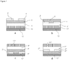
- FIG. 1 illustrates the four common types of OFET structures: top-contact bottom-gate structure (a), bottom-contact bottom-gate structure (b), bottom-contact top-gate structure (c), and top-contact top-gate structure (d).
- an OFET can include a dielectric layer (e.g., shown as 8, 8', 8", and 8"' in Figure 1a, 1b, 1c, and 1d , respectively), a semiconductor layer (e.g., shown as 6, 6', 6", and 6"' in Figure 1a, 1b, 1c, and 1d , respectively), a gate contact (e.g., shown as 10, 10', 10", and 10"' in Figure 1a, 1b, 1c, and 1d , respectively), a substrate (e.g., shown as 12, 12', 12", and 12"' in Figure 1a, 1b, 1c, and 1d , respectively), and source and drain contacts (e.g., shown as 2, 2', 2", 2"', 4, 4', 4", and 4"' in Figure 1a, 1b, 1c, and 1d , respectively).
- a dielectric layer e.g., shown as 8, 8', 8", and 8"' in Figure 1a, 1b, 1c, and
- OTFT devices can be fabricated with the present compounds on doped silicon substrates, using SiO 2 as the dielectric, in top-contact geometries.
- the active semiconducting layer which incorporates at least a material of the present teachings can be deposited at room temperature or at an elevated temperature.
- the active semiconducting layer which incorporates at least a compound of the present teachings can be applied by spin-coating or printing as described herein.
- metallic contacts can be patterned on top of the films using shadow masks.
- silicon wafers with a 200 nm thick thermally grown silicon dioxide layer were used as substrates.
- Hexamethyldisilazane was deposited out of the gas phase at 120 °C.
- the semiconductor polymeric film was prepared by pincoating (3000 rpm, 60 s) a 5 mg ml -1 1,2-dichlorobenzene solution (roughly 47.5 nm thick).
Landscapes
- Chemical & Material Sciences (AREA)
- Engineering & Computer Science (AREA)
- Materials Engineering (AREA)
- Medicinal Chemistry (AREA)
- Polymers & Plastics (AREA)
- Organic Chemistry (AREA)
- Health & Medical Sciences (AREA)
- Chemical Kinetics & Catalysis (AREA)
- Thin Film Transistor (AREA)
- Polyoxymethylene Polymers And Polymers With Carbon-To-Carbon Bonds (AREA)
- Electroluminescent Light Sources (AREA)
- Heterocyclic Carbon Compounds Containing A Hetero Ring Having Oxygen Or Sulfur (AREA)
- Paints Or Removers (AREA)
Claims (8)
- Dithienobenzothieno[3,2-b]thiophen-Copolymere der Formel
 pi für
p, p' und u' unabhängig aus -S-, -0-, -CH=, =CH-, -CR6=, =CR6-, -C(O)-, -C(C(CN)2)-, -N=, =N-, -NH-, -NR3-, -SiRc=, =SiRc- und -SiR7Rc- ausgewählt sind;R6 bei jedem Auftreten unabhängig aus a) Halogen, b) -CN, c) -NO2, d) N(Rc)2, e) -ORc, f) -C(O)Rc, g) -C(O)ORc, h) -C(O)N(Rc)2, i) einer C1-40-Alkylgruppe, j) einer C2-40-Alkenylgruppe, k) einer C2-40-Alkinylgruppe, 1) einer C1-40-Alkoxygruppe, m) einer C1-40-Alkylthiogruppe, n) einer C1-40-Halogenalkylgruppe, o) einer -Y-C3-14-Cycloalkylgruppe, p) einer -Y-C6-14-Arylgruppe, q) einer -Y-Cycloheteroalkylgruppe, wobei die Cycloheteroalkylgruppe 3-14-gliedrig ist, und r) einer -Y-Heteroarylgruppe, wobei die Heteroarylgruppe 5-14-gliedrig ist, ausgewählt ist;R1, R2 und R3 bei jedem Auftreten unabhängig für H, ein Halogen, CN, eine C1-30-Alkylgruppe, eine C2-30-Alkenylgruppe, eine C1-30-Halogenalkylgruppe, eine C2-30-Alkinylgruppe, eine C1-30-Alkoxygruppe, eine C(O)-C1-20-Alkylgruppe, eine C(O)-OC1-20-Alkylgruppe, eine Y-C3-10-Cycloalkylgruppe, eine -Y-Cycloheteroalkylgruppe, wobei die Cyclohetero-alkylgruppe 3-12-gliedrig ist, jeweils substituiert durch 1-5 Substituenten, die aus einem Halogen, -CN, einer C1-6-Alkylgruppe, einer C1-6-Alkoxygruppe und einer C1-6-Halogenalkylgruppe ausgewählt sind, -L-Ar1, -L-Ar1-Ar1, -L-Ar1-R4 oder -L-Ar1-Ar1-R4 stehen;wobei:L bei jedem Auftreten unabhängig für -0-, -Y-O-Y-, -S-, -S(O)-, -Y-S-Y-, -C(O)-, -NRcC(O)-, -NRc-, -SiRc 2-, -Y-[SiRc 2 ] -Y-, eine zweiwertige C2-30-Alkylgruppe, eine zweiwertige C1-30-Alkenylgruppe, eine zweiwertige C1-30-Halogenalkylgruppe oder eine kovalente Bindung steht;wobei:Rc bei jedem Auftreten für H, eine C1-20-Alkylgruppe oder eine -Y-C6-14-Arylgruppe steht;Ar1 bei jedem Auftreten unabhängig für eine C6-14-Arylgruppe oder eine 5-14-gliedrige Heteroarylgruppe, jeweils substituiert durch 1-5 Substituenten, die aus einem Halogen, -CN, einer C1-6-Alkylgruppe, einer C1-6-Alkoxygruppe und einer C1-6-Halogenalkylgruppe ausgewählt sind, steht; undR4 bei jedem Auftreten unabhängig für eine C1-20-Alkylgruppe, eine C2-20-Alkenylgruppe, eine C1-20-Halogenalkylgruppe, eine C1-20-Alkoxygruppe, -L'-Ar2, -L'-Ar2-Ar2, -L'-Ar2-R5 oder -L'-Ar2-Ar2-R5 steht;wobei:L' bei jedem Auftreten unabhängig für -0-, -Y-O-Y-, -S-, -S(O)-, -Y-S-Y-, -C(O)-, -NRcC(O)-, -NRc-, -SiRc 2-, -Y-[SiRc 2]-Y-, eine zweiwertige C1-20-Alkylgruppe, eine zweiwertige C1-20-Alkenylgruppe, eine zweiwertige C1-20-Halogenalkylgruppe oder eine kovalente Bindung steht;Ar2 bei jedem Auftreten unabhängig für eine C6-14-Arylgruppe oder eine 5-14-gliedrige Heteroarylgruppe, jeweils substituiert durch 1-5 Substituenten, die aus einem Halogen, -CN, einer C1-6-Alkylgruppe, einer C1-6-Alkoxygruppe und einer C1-6-Halogenalkylgruppe ausgewählt sind, steht;R5 bei jedem Auftreten für eine C1-20-Alkylgruppe, eine C2-20-Alkenylgruppe, eine C1-20-Halogen-alkylgruppe oder eine C1-20-Alkoxygruppe steht;und Y bei jedem Auftreten unabhängig für eine zweiwertige C1-6-Alkylgruppe, eine zweiwertige C1-6-Halogenalkylgruppe oder eine kovalente Bindung steht;n = 0, 1, 2 undo = 5-1000. - Verwendung des Polymers nach Anspruch 1 als Halbleiter oder Ladungstransportmaterialien, als Dünnschichttransistoren (Thin-Film Transistors, TFTs) oder in Halbleiterkomponenten für organische Leuchtdioden (Organic Light-Emitting Diodes, OLEDs), für Photovoltaikkomponenten oder in Sensoren, als Elektrodenmaterial in Batterien, als Lichtwellenleiter oder für Elektrophotographie-Anwendungen.
- Zusammensetzung, umfassend ein oder mehrere Polymere nach Anspruch 1 in einem flüssigen Medium gelöst oder dispergiert.
- Dünnschichthalbleiter, umfassend ein oder mehrere Polymere nach Anspruch 1.
- Verbund, umfassend ein Substrat und den darauf aufgebrachten Dünnschichthalbleiter nach Anspruch 4.
- Verfahren zur Herstellung eines Verbunds nach Anspruch 5, bei dem man das Polymer nach Anspruch 1 in einem flüssigen Medium löst oder dispergiert, was eine Lösung ergibt, die Lösung auf ein Substrat aufbringt und das Lösungsmittel entfernt, was einen Dünnschichthalbleiter auf dem Substrat ergibt.
- Verfahren nach Anspruch 6, bei dem das Aufbringen der Lösung durch Aufschleudern, Auftropfen, Eintauchbeschichten oder Drucken erfolgt.
- Feldeffekttransistorvorrichtung, umfassend den Dünnschichthalbleiter nach Anspruch 4 oder den Verbund nach Anspruch 5.
Applications Claiming Priority (2)
| Application Number | Priority Date | Filing Date | Title |
|---|---|---|---|
| US26577809P | 2009-12-02 | 2009-12-02 | |
| PCT/EP2010/068365 WO2011067192A2 (en) | 2009-12-02 | 2010-11-29 | Dithienobenzo-thieno[3,2-b]thiophene-copolymer and its use as high performance solution processable semiconducting polymer |
Publications (2)
| Publication Number | Publication Date |
|---|---|
| EP2507286A2 EP2507286A2 (de) | 2012-10-10 |
| EP2507286B1 true EP2507286B1 (de) | 2017-07-05 |
Family
ID=43912750
Family Applications (1)
| Application Number | Title | Priority Date | Filing Date |
|---|---|---|---|
| EP10785057.0A Not-in-force EP2507286B1 (de) | 2009-12-02 | 2010-11-29 | Dithienobenzo-thieno[3,2-b]thiophene-copolymer und dessen verwendung als aus der lösung verarbeitbares halbleitendes hochleistungspolymer |
Country Status (6)
| Country | Link |
|---|---|
| US (1) | US8389670B2 (de) |
| EP (1) | EP2507286B1 (de) |
| JP (1) | JP5774599B2 (de) |
| KR (1) | KR101780083B1 (de) |
| CN (1) | CN102639591B (de) |
| WO (1) | WO2011067192A2 (de) |
Families Citing this family (40)
| Publication number | Priority date | Publication date | Assignee | Title |
|---|---|---|---|---|
| CN102149750B (zh) | 2008-07-18 | 2014-04-23 | 芝加哥大学 | 半导体聚合物 |
| EP2697283A4 (de) | 2011-04-15 | 2015-12-16 | Univ Chicago | Halbleiterpolymere |
| JP5742494B2 (ja) * | 2011-06-10 | 2015-07-01 | 住友化学株式会社 | 高分子化合物及びそれを用いた電子素子 |
| KR20140129080A (ko) * | 2012-02-03 | 2014-11-06 | 더 유니버시티 오브 시카고 | 반도체성 고분자 |
| US20130247992A1 (en) * | 2012-03-22 | 2013-09-26 | Polyera Corporation | Polymeric Blends and Related Optoelectronic Devices |
| US20150295193A1 (en) * | 2012-11-22 | 2015-10-15 | University of Seoul Industry Cooperation Foundatio n | Semiconductor device using paper as a substrate and method of manufacturing the same |
| WO2014087300A1 (en) * | 2012-12-03 | 2014-06-12 | Basf Se | Heteroacene compounds for organic electronics |
| EP2936052B1 (de) | 2012-12-19 | 2021-04-28 | Basf Se | Detektor zur optischen erfassung mindestens eines objekts |
| CN104119501A (zh) * | 2013-04-25 | 2014-10-29 | 海洋王照明科技股份有限公司 | 含噻吩并噻吩-二噻吩并苯并噻二唑-苯并噻二唑类共轭聚合物及其制备方法与应用 |
| CN104119503A (zh) * | 2013-04-25 | 2014-10-29 | 海洋王照明科技股份有限公司 | 含噻吩并噻吩-二噻吩并苯并三唑-苯并噻二唑类共轭聚合物及其制备方法与应用 |
| CN104119502A (zh) * | 2013-04-25 | 2014-10-29 | 海洋王照明科技股份有限公司 | 含噻吩并噻吩-二噻吩并苯并噁二唑-苯并噻二唑类共轭聚合物及其制备方法与应用 |
| CN104211921A (zh) * | 2013-05-29 | 2014-12-17 | 海洋王照明科技股份有限公司 | 共轭聚合物及其制备方法与应用 |
| CN104211912A (zh) * | 2013-05-29 | 2014-12-17 | 海洋王照明科技股份有限公司 | 共轭聚合物及其制备方法与应用 |
| CN104211913A (zh) * | 2013-05-29 | 2014-12-17 | 海洋王照明科技股份有限公司 | 共轭聚合物及其制备方法与应用 |
| CN104211915A (zh) * | 2013-05-29 | 2014-12-17 | 海洋王照明科技股份有限公司 | 共轭聚合物及其制备方法与应用 |
| JP6440696B2 (ja) | 2013-06-13 | 2018-12-19 | ビーエーエスエフ ソシエタス・ヨーロピアBasf Se | 少なくとも1つの物体の方位を光学的に検出する検出器 |
| CN105210190A (zh) | 2013-06-13 | 2015-12-30 | 巴斯夫欧洲公司 | 光学检测器及其制造方法 |
| JP2016529473A (ja) | 2013-06-13 | 2016-09-23 | ビーエーエスエフ ソシエタス・ヨーロピアBasf Se | 少なくとも1つの物体を光学的に検出する検出器 |
| CN103408733B (zh) * | 2013-08-13 | 2015-09-30 | 武汉理工大学 | 二硒吩并苯并二茚类共轭聚合物半导体材料及其应用 |
| JP6483127B2 (ja) | 2013-08-19 | 2019-03-13 | ビーエーエスエフ ソシエタス・ヨーロピアBasf Se | 少なくとも1つの対象物の位置を求めるための検出器 |
| CN105637320B (zh) | 2013-08-19 | 2018-12-14 | 巴斯夫欧洲公司 | 光学检测器 |
| WO2015097078A2 (en) | 2013-12-24 | 2015-07-02 | Solvay Sa | Small molecule heteroacenes as semiconductors |
| JP2015141912A (ja) * | 2014-01-27 | 2015-08-03 | 富士フイルム株式会社 | 有機薄膜トランジスタ、有機半導体薄膜および有機半導体材料 |
| JP6660931B2 (ja) | 2014-07-08 | 2020-03-11 | ビーエーエスエフ ソシエタス・ヨーロピアBasf Se | 少なくとも1つの物体の位置を決定するための検出器 |
| WO2016009890A1 (ja) * | 2014-07-18 | 2016-01-21 | 富士フイルム株式会社 | 有機半導体膜形成用組成物、並びに、有機半導体素子及びその製造方法 |
| JP6578006B2 (ja) | 2014-09-29 | 2019-09-18 | ビーエーエスエフ ソシエタス・ヨーロピアBasf Se | 少なくとも1個の物体の位置を光学的に求めるための検出器 |
| EP3230841B1 (de) | 2014-12-09 | 2019-07-03 | Basf Se | Optischer detektor |
| CN107438775B (zh) | 2015-01-30 | 2022-01-21 | 特里纳米克斯股份有限公司 | 用于至少一个对象的光学检测的检测器 |
| US10955936B2 (en) | 2015-07-17 | 2021-03-23 | Trinamix Gmbh | Detector for optically detecting at least one object |
| EP3350988B1 (de) | 2015-09-14 | 2019-08-07 | trinamiX GmbH | 3d kamera |
| WO2018019921A1 (en) | 2016-07-29 | 2018-02-01 | Trinamix Gmbh | Optical sensor and detector for optical detection |
| EP3532864B1 (de) | 2016-10-25 | 2024-08-28 | trinamiX GmbH | Detektor für eine optische detektion mindestens eines objekts |
| WO2018077870A1 (en) | 2016-10-25 | 2018-05-03 | Trinamix Gmbh | Nfrared optical detector with integrated filter |
| KR102502094B1 (ko) | 2016-11-17 | 2023-02-21 | 트리나미엑스 게엠베하 | 적어도 하나의 피사체를 광학적으로 검출하기 위한 검출기 |
| US11860292B2 (en) | 2016-11-17 | 2024-01-02 | Trinamix Gmbh | Detector and methods for authenticating at least one object |
| KR102623150B1 (ko) | 2017-04-20 | 2024-01-11 | 트리나미엑스 게엠베하 | 광 검출기 |
| CN110998223B (zh) | 2017-06-26 | 2021-10-29 | 特里纳米克斯股份有限公司 | 用于确定至少一个对像的位置的检测器 |
| US11296290B2 (en) | 2018-03-07 | 2022-04-05 | Clap Co., Ltd. | Patterning method for preparing top-gate, bottom-contact organic field effect transistors |
| JP7075682B2 (ja) | 2018-03-08 | 2022-05-26 | クラップ カンパニー リミテッド | 半導電性単層カーボンナノチューブ及び有機半導電性材料を含む有機電界効果トランジスタ |
| CN112074548B (zh) | 2018-06-26 | 2023-07-25 | Clap有限公司 | 作为电介质的乙烯醚类聚合物 |
Family Cites Families (18)
| Publication number | Priority date | Publication date | Assignee | Title |
|---|---|---|---|---|
| US5198153A (en) | 1989-05-26 | 1993-03-30 | International Business Machines Corporation | Electrically conductive polymeric |
| JP3224829B2 (ja) | 1991-08-15 | 2001-11-05 | 株式会社東芝 | 有機電界効果型素子 |
| WO1996021659A1 (en) | 1995-01-10 | 1996-07-18 | University Of Technology, Sydney | Organic semiconductor |
| WO1999012989A1 (en) * | 1997-09-05 | 1999-03-18 | Cambridge Display Technology Ltd. | Compounds for electronic devices |
| ATE413423T1 (de) * | 2003-08-28 | 2008-11-15 | Merck Patent Gmbh | Mono-, oligo- und polythieno(2,3-b)thiophene |
| DE602004024629D1 (de) | 2003-10-15 | 2010-01-28 | Merck Patent Gmbh | Polybenzodithiophene |
| KR20070112791A (ko) | 2005-03-11 | 2007-11-27 | 메르크 파텐트 게엠베하 | 티오펜 및 셀레노펜 함유 단량체, 올리고머 및 중합체 |
| ATE465166T1 (de) | 2005-06-09 | 2010-05-15 | Merck Patent Gmbh | Monomere, oligomere und polymere von thieno ä3,4- dü thiazol |
| JP5164134B2 (ja) * | 2006-03-10 | 2013-03-13 | 住友化学株式会社 | 縮合環化合物及びその製造方法、重合体、これらを含む有機薄膜、並びに、これを備える有機薄膜素子及び有機薄膜トランジスタ |
| US8895692B2 (en) | 2006-03-10 | 2014-11-25 | Sumitomo Chemical Company, Limited | Fused ring compound and method for producing same, polymer, organic thin film containing those, and organic thin film device and organic thin film transistor comprising such organic thin film |
| EP2067782B2 (de) * | 2006-08-28 | 2018-06-27 | Tosoh Corporation | Heteroacenderivat, tetrahalogenterphenylderivat und verfahren zu ihrer herstellung |
| CA2606985C (en) | 2006-10-25 | 2011-02-01 | Xerox Corporation | Electronic devices |
| US7820782B2 (en) * | 2006-10-25 | 2010-10-26 | Xerox Corporation | Poly(dithienylbenzo[1,2-b:4,5-b′]dithiophene) polymers |
| KR101314998B1 (ko) * | 2006-12-13 | 2013-10-04 | 삼성전자주식회사 | 헤테로아센 화합물, 이를 포함하는 유기 박막 및 당해 박막을 포함하는 전자 소자 |
| JP5138422B2 (ja) * | 2008-02-29 | 2013-02-06 | 株式会社リコー | ベンゾチエノ[3,2−b]ベンゾチオフェン構造を含む重合体 |
| CN102084436B (zh) | 2008-07-02 | 2012-10-17 | 巴斯夫欧洲公司 | 聚(5,5′-二(噻吩-2-基)苯并[2,1-b;3,4-b′]二噻吩)及其作为高性能可溶液加工半导体聚合物的用途 |
| TWI471328B (zh) | 2008-07-02 | 2015-02-01 | 巴地斯顏料化工廠 | 以二噻吩并〔2,3-d:2’,3’-d’〕苯并〔1,2-b:4,5-b’〕二噻吩為主之高效能溶液可加工之半導體 |
| US20110136973A1 (en) | 2008-08-11 | 2011-06-09 | Basf Se | Polybenzothiophene polymers and process for their preparation |
-
2010
- 2010-11-29 US US13/511,890 patent/US8389670B2/en not_active Expired - Fee Related
- 2010-11-29 KR KR1020127016964A patent/KR101780083B1/ko not_active Expired - Fee Related
- 2010-11-29 CN CN201080054412.3A patent/CN102639591B/zh not_active Expired - Fee Related
- 2010-11-29 EP EP10785057.0A patent/EP2507286B1/de not_active Not-in-force
- 2010-11-29 JP JP2012541429A patent/JP5774599B2/ja not_active Expired - Fee Related
- 2010-11-29 WO PCT/EP2010/068365 patent/WO2011067192A2/en not_active Ceased
Also Published As
| Publication number | Publication date |
|---|---|
| US20120289672A1 (en) | 2012-11-15 |
| KR20120116427A (ko) | 2012-10-22 |
| US8389670B2 (en) | 2013-03-05 |
| CN102639591A (zh) | 2012-08-15 |
| JP2013512975A (ja) | 2013-04-18 |
| KR101780083B1 (ko) | 2017-10-10 |
| EP2507286A2 (de) | 2012-10-10 |
| CN102639591B (zh) | 2015-05-13 |
| WO2011067192A3 (en) | 2011-09-15 |
| WO2011067192A2 (en) | 2011-06-09 |
| JP5774599B2 (ja) | 2015-09-09 |
Similar Documents
| Publication | Publication Date | Title |
|---|---|---|
| EP2507286B1 (de) | Dithienobenzo-thieno[3,2-b]thiophene-copolymer und dessen verwendung als aus der lösung verarbeitbares halbleitendes hochleistungspolymer | |
| EP2297748B1 (de) | Poly(5,5'bis(thiophen-2-yl)-benzo[2,1-b;3,4-b']dithiophen) und dessen verwendung als aus der lösung verarbeitbares hochleistungs-halbleiter-polymer | |
| KR101855051B1 (ko) | [2,3-d:2',3'-d']벤조[1,2-b:4,5-b']디티오펜을 베이스로 하는 고성능 용액 가공성 반도체 | |
| KR101561322B1 (ko) | 교대 도너 억셉터 공중합체를 주성분으로 하는 고성능 용액 가공성 반도체 중합체 | |
| EP2438104B1 (de) | Kondensierte bithiophen-vinylen-polymere | |
| US20110136973A1 (en) | Polybenzothiophene polymers and process for their preparation | |
| EP2626375A1 (de) | Aus Dithienylvinylen-Copolymeren hergestellte Halbleitermaterialien | |
| KR20130040830A (ko) | 어닐링된 디티오펜 공중합체 | |
| EP2729514A1 (de) | Dithienophthalimid-halbleiterpolymere | |
| KR20060060776A (ko) | 유기 용매 용해성 폴리티오펜 유도체의 제조방법 및 그의용도 |
Legal Events
| Date | Code | Title | Description |
|---|---|---|---|
| PUAI | Public reference made under article 153(3) epc to a published international application that has entered the european phase |
Free format text: ORIGINAL CODE: 0009012 |
|
| 17P | Request for examination filed |
Effective date: 20120702 |
|
| AK | Designated contracting states |
Kind code of ref document: A2 Designated state(s): AL AT BE BG CH CY CZ DE DK EE ES FI FR GB GR HR HU IE IS IT LI LT LU LV MC MK MT NL NO PL PT RO RS SE SI SK SM TR |
|
| DAX | Request for extension of the european patent (deleted) | ||
| 17Q | First examination report despatched |
Effective date: 20160923 |
|
| GRAP | Despatch of communication of intention to grant a patent |
Free format text: ORIGINAL CODE: EPIDOSNIGR1 |
|
| INTG | Intention to grant announced |
Effective date: 20170127 |
|
| GRAS | Grant fee paid |
Free format text: ORIGINAL CODE: EPIDOSNIGR3 |
|
| GRAA | (expected) grant |
Free format text: ORIGINAL CODE: 0009210 |
|
| AK | Designated contracting states |
Kind code of ref document: B1 Designated state(s): AL AT BE BG CH CY CZ DE DK EE ES FI FR GB GR HR HU IE IS IT LI LT LU LV MC MK MT NL NO PL PT RO RS SE SI SK SM TR |
|
| REG | Reference to a national code |
Ref country code: GB Ref legal event code: FG4D |
|
| REG | Reference to a national code |
Ref country code: CH Ref legal event code: EP |
|
| REG | Reference to a national code |
Ref country code: AT Ref legal event code: REF Ref document number: 906566 Country of ref document: AT Kind code of ref document: T Effective date: 20170715 |
|
| REG | Reference to a national code |
Ref country code: IE Ref legal event code: FG4D |
|
| REG | Reference to a national code |
Ref country code: DE Ref legal event code: R096 Ref document number: 602010043467 Country of ref document: DE |
|
| REG | Reference to a national code |
Ref country code: NL Ref legal event code: MP Effective date: 20170705 |
|
| REG | Reference to a national code |
Ref country code: AT Ref legal event code: MK05 Ref document number: 906566 Country of ref document: AT Kind code of ref document: T Effective date: 20170705 |
|
| REG | Reference to a national code |
Ref country code: LT Ref legal event code: MG4D Ref country code: FR Ref legal event code: PLFP Year of fee payment: 8 |
|
| PG25 | Lapsed in a contracting state [announced via postgrant information from national office to epo] |
Ref country code: NO Free format text: LAPSE BECAUSE OF FAILURE TO SUBMIT A TRANSLATION OF THE DESCRIPTION OR TO PAY THE FEE WITHIN THE PRESCRIBED TIME-LIMIT Effective date: 20171005 Ref country code: LT Free format text: LAPSE BECAUSE OF FAILURE TO SUBMIT A TRANSLATION OF THE DESCRIPTION OR TO PAY THE FEE WITHIN THE PRESCRIBED TIME-LIMIT Effective date: 20170705 Ref country code: HR Free format text: LAPSE BECAUSE OF FAILURE TO SUBMIT A TRANSLATION OF THE DESCRIPTION OR TO PAY THE FEE WITHIN THE PRESCRIBED TIME-LIMIT Effective date: 20170705 Ref country code: FI Free format text: LAPSE BECAUSE OF FAILURE TO SUBMIT A TRANSLATION OF THE DESCRIPTION OR TO PAY THE FEE WITHIN THE PRESCRIBED TIME-LIMIT Effective date: 20170705 Ref country code: AT Free format text: LAPSE BECAUSE OF FAILURE TO SUBMIT A TRANSLATION OF THE DESCRIPTION OR TO PAY THE FEE WITHIN THE PRESCRIBED TIME-LIMIT Effective date: 20170705 Ref country code: NL Free format text: LAPSE BECAUSE OF FAILURE TO SUBMIT A TRANSLATION OF THE DESCRIPTION OR TO PAY THE FEE WITHIN THE PRESCRIBED TIME-LIMIT Effective date: 20170705 Ref country code: SE Free format text: LAPSE BECAUSE OF FAILURE TO SUBMIT A TRANSLATION OF THE DESCRIPTION OR TO PAY THE FEE WITHIN THE PRESCRIBED TIME-LIMIT Effective date: 20170705 |
|
| PG25 | Lapsed in a contracting state [announced via postgrant information from national office to epo] |
Ref country code: BG Free format text: LAPSE BECAUSE OF FAILURE TO SUBMIT A TRANSLATION OF THE DESCRIPTION OR TO PAY THE FEE WITHIN THE PRESCRIBED TIME-LIMIT Effective date: 20171005 Ref country code: IS Free format text: LAPSE BECAUSE OF FAILURE TO SUBMIT A TRANSLATION OF THE DESCRIPTION OR TO PAY THE FEE WITHIN THE PRESCRIBED TIME-LIMIT Effective date: 20171105 Ref country code: LV Free format text: LAPSE BECAUSE OF FAILURE TO SUBMIT A TRANSLATION OF THE DESCRIPTION OR TO PAY THE FEE WITHIN THE PRESCRIBED TIME-LIMIT Effective date: 20170705 Ref country code: RS Free format text: LAPSE BECAUSE OF FAILURE TO SUBMIT A TRANSLATION OF THE DESCRIPTION OR TO PAY THE FEE WITHIN THE PRESCRIBED TIME-LIMIT Effective date: 20170705 Ref country code: ES Free format text: LAPSE BECAUSE OF FAILURE TO SUBMIT A TRANSLATION OF THE DESCRIPTION OR TO PAY THE FEE WITHIN THE PRESCRIBED TIME-LIMIT Effective date: 20170705 Ref country code: PL Free format text: LAPSE BECAUSE OF FAILURE TO SUBMIT A TRANSLATION OF THE DESCRIPTION OR TO PAY THE FEE WITHIN THE PRESCRIBED TIME-LIMIT Effective date: 20170705 Ref country code: GR Free format text: LAPSE BECAUSE OF FAILURE TO SUBMIT A TRANSLATION OF THE DESCRIPTION OR TO PAY THE FEE WITHIN THE PRESCRIBED TIME-LIMIT Effective date: 20171006 |
|
| REG | Reference to a national code |
Ref country code: DE Ref legal event code: R097 Ref document number: 602010043467 Country of ref document: DE |
|
| PG25 | Lapsed in a contracting state [announced via postgrant information from national office to epo] |
Ref country code: RO Free format text: LAPSE BECAUSE OF FAILURE TO SUBMIT A TRANSLATION OF THE DESCRIPTION OR TO PAY THE FEE WITHIN THE PRESCRIBED TIME-LIMIT Effective date: 20170705 Ref country code: DK Free format text: LAPSE BECAUSE OF FAILURE TO SUBMIT A TRANSLATION OF THE DESCRIPTION OR TO PAY THE FEE WITHIN THE PRESCRIBED TIME-LIMIT Effective date: 20170705 Ref country code: CZ Free format text: LAPSE BECAUSE OF FAILURE TO SUBMIT A TRANSLATION OF THE DESCRIPTION OR TO PAY THE FEE WITHIN THE PRESCRIBED TIME-LIMIT Effective date: 20170705 |
|
| PLBE | No opposition filed within time limit |
Free format text: ORIGINAL CODE: 0009261 |
|
| STAA | Information on the status of an ep patent application or granted ep patent |
Free format text: STATUS: NO OPPOSITION FILED WITHIN TIME LIMIT |
|
| PG25 | Lapsed in a contracting state [announced via postgrant information from national office to epo] |
Ref country code: EE Free format text: LAPSE BECAUSE OF FAILURE TO SUBMIT A TRANSLATION OF THE DESCRIPTION OR TO PAY THE FEE WITHIN THE PRESCRIBED TIME-LIMIT Effective date: 20170705 Ref country code: SM Free format text: LAPSE BECAUSE OF FAILURE TO SUBMIT A TRANSLATION OF THE DESCRIPTION OR TO PAY THE FEE WITHIN THE PRESCRIBED TIME-LIMIT Effective date: 20170705 Ref country code: SK Free format text: LAPSE BECAUSE OF FAILURE TO SUBMIT A TRANSLATION OF THE DESCRIPTION OR TO PAY THE FEE WITHIN THE PRESCRIBED TIME-LIMIT Effective date: 20170705 |
|
| 26N | No opposition filed |
Effective date: 20180406 |
|
| PG25 | Lapsed in a contracting state [announced via postgrant information from national office to epo] |
Ref country code: MC Free format text: LAPSE BECAUSE OF FAILURE TO SUBMIT A TRANSLATION OF THE DESCRIPTION OR TO PAY THE FEE WITHIN THE PRESCRIBED TIME-LIMIT Effective date: 20170705 |
|
| PG25 | Lapsed in a contracting state [announced via postgrant information from national office to epo] |
Ref country code: CH Free format text: LAPSE BECAUSE OF NON-PAYMENT OF DUE FEES Effective date: 20171130 Ref country code: LI Free format text: LAPSE BECAUSE OF NON-PAYMENT OF DUE FEES Effective date: 20171130 |
|
| PG25 | Lapsed in a contracting state [announced via postgrant information from national office to epo] |
Ref country code: LU Free format text: LAPSE BECAUSE OF NON-PAYMENT OF DUE FEES Effective date: 20171129 Ref country code: SI Free format text: LAPSE BECAUSE OF FAILURE TO SUBMIT A TRANSLATION OF THE DESCRIPTION OR TO PAY THE FEE WITHIN THE PRESCRIBED TIME-LIMIT Effective date: 20170705 |
|
| REG | Reference to a national code |
Ref country code: BE Ref legal event code: MM Effective date: 20171130 |
|
| REG | Reference to a national code |
Ref country code: IE Ref legal event code: MM4A |
|
| PG25 | Lapsed in a contracting state [announced via postgrant information from national office to epo] |
Ref country code: MT Free format text: LAPSE BECAUSE OF NON-PAYMENT OF DUE FEES Effective date: 20171129 |
|
| PG25 | Lapsed in a contracting state [announced via postgrant information from national office to epo] |
Ref country code: IE Free format text: LAPSE BECAUSE OF NON-PAYMENT OF DUE FEES Effective date: 20171129 |
|
| PG25 | Lapsed in a contracting state [announced via postgrant information from national office to epo] |
Ref country code: BE Free format text: LAPSE BECAUSE OF NON-PAYMENT OF DUE FEES Effective date: 20171130 |
|
| PG25 | Lapsed in a contracting state [announced via postgrant information from national office to epo] |
Ref country code: HU Free format text: LAPSE BECAUSE OF FAILURE TO SUBMIT A TRANSLATION OF THE DESCRIPTION OR TO PAY THE FEE WITHIN THE PRESCRIBED TIME-LIMIT; INVALID AB INITIO Effective date: 20101129 |
|
| PG25 | Lapsed in a contracting state [announced via postgrant information from national office to epo] |
Ref country code: CY Free format text: LAPSE BECAUSE OF NON-PAYMENT OF DUE FEES Effective date: 20170705 |
|
| PG25 | Lapsed in a contracting state [announced via postgrant information from national office to epo] |
Ref country code: MK Free format text: LAPSE BECAUSE OF FAILURE TO SUBMIT A TRANSLATION OF THE DESCRIPTION OR TO PAY THE FEE WITHIN THE PRESCRIBED TIME-LIMIT Effective date: 20170705 |
|
| PG25 | Lapsed in a contracting state [announced via postgrant information from national office to epo] |
Ref country code: TR Free format text: LAPSE BECAUSE OF FAILURE TO SUBMIT A TRANSLATION OF THE DESCRIPTION OR TO PAY THE FEE WITHIN THE PRESCRIBED TIME-LIMIT Effective date: 20170705 |
|
| PG25 | Lapsed in a contracting state [announced via postgrant information from national office to epo] |
Ref country code: PT Free format text: LAPSE BECAUSE OF FAILURE TO SUBMIT A TRANSLATION OF THE DESCRIPTION OR TO PAY THE FEE WITHIN THE PRESCRIBED TIME-LIMIT Effective date: 20170705 |
|
| PG25 | Lapsed in a contracting state [announced via postgrant information from national office to epo] |
Ref country code: AL Free format text: LAPSE BECAUSE OF FAILURE TO SUBMIT A TRANSLATION OF THE DESCRIPTION OR TO PAY THE FEE WITHIN THE PRESCRIBED TIME-LIMIT Effective date: 20170705 |
|
| REG | Reference to a national code |
Ref country code: DE Ref legal event code: R082 Ref document number: 602010043467 Country of ref document: DE Representative=s name: REITSTOETTER - KINZEBACH, DE Ref country code: DE Ref legal event code: R082 Ref document number: 602010043467 Country of ref document: DE |
|
| REG | Reference to a national code |
Ref country code: GB Ref legal event code: 732E Free format text: REGISTERED BETWEEN 20220324 AND 20220330 |
|
| REG | Reference to a national code |
Ref country code: DE Ref legal event code: R081 Ref document number: 602010043467 Country of ref document: DE Owner name: MAX-PLANCK-GESELLSCHAFT ZUR FOERDERUNG DER WIS, DE Free format text: FORMER OWNERS: BASF SE, 67063 LUDWIGSHAFEN, DE; MAX-PLANCK-GESELLSCHAFT ZUR FOERDERUNG DER WISSENSCHAFTEN E.V., 80539 MUENCHEN, DE Ref country code: DE Ref legal event code: R081 Ref document number: 602010043467 Country of ref document: DE Owner name: CLAP CO., LTD., KR Free format text: FORMER OWNERS: BASF SE, 67063 LUDWIGSHAFEN, DE; MAX-PLANCK-GESELLSCHAFT ZUR FOERDERUNG DER WISSENSCHAFTEN E.V., 80539 MUENCHEN, DE Ref country code: DE Ref legal event code: R082 Ref document number: 602010043467 Country of ref document: DE Representative=s name: REITSTOETTER - KINZEBACH, DE |
|
| PGFP | Annual fee paid to national office [announced via postgrant information from national office to epo] |
Ref country code: FR Payment date: 20230929 Year of fee payment: 14 |
|
| PGFP | Annual fee paid to national office [announced via postgrant information from national office to epo] |
Ref country code: GB Payment date: 20231006 Year of fee payment: 14 |
|
| PGFP | Annual fee paid to national office [announced via postgrant information from national office to epo] |
Ref country code: IT Payment date: 20231010 Year of fee payment: 14 Ref country code: DE Payment date: 20231003 Year of fee payment: 14 |
|
| REG | Reference to a national code |
Ref country code: DE Ref legal event code: R119 Ref document number: 602010043467 Country of ref document: DE |
|
| GBPC | Gb: european patent ceased through non-payment of renewal fee |
Effective date: 20241129 |
|
| PG25 | Lapsed in a contracting state [announced via postgrant information from national office to epo] |
Ref country code: DE Free format text: LAPSE BECAUSE OF NON-PAYMENT OF DUE FEES Effective date: 20250603 |
|
| PG25 | Lapsed in a contracting state [announced via postgrant information from national office to epo] |
Ref country code: IT Free format text: LAPSE BECAUSE OF NON-PAYMENT OF DUE FEES Effective date: 20241129 |
|
| PG25 | Lapsed in a contracting state [announced via postgrant information from national office to epo] |
Ref country code: GB Free format text: LAPSE BECAUSE OF NON-PAYMENT OF DUE FEES Effective date: 20241129 |
|
| PG25 | Lapsed in a contracting state [announced via postgrant information from national office to epo] |
Ref country code: FR Free format text: LAPSE BECAUSE OF NON-PAYMENT OF DUE FEES Effective date: 20241130 |