EP2500946A2 - Organische lichtemittierende Anzeige und Verfahren zu ihrer Herstellung - Google Patents
Organische lichtemittierende Anzeige und Verfahren zu ihrer Herstellung Download PDFInfo
- Publication number
- EP2500946A2 EP2500946A2 EP12159126A EP12159126A EP2500946A2 EP 2500946 A2 EP2500946 A2 EP 2500946A2 EP 12159126 A EP12159126 A EP 12159126A EP 12159126 A EP12159126 A EP 12159126A EP 2500946 A2 EP2500946 A2 EP 2500946A2
- Authority
- EP
- European Patent Office
- Prior art keywords
- layer
- electrode
- organic light
- electrode layer
- capacitor
- Prior art date
- Legal status (The legal status is an assumption and is not a legal conclusion. Google has not performed a legal analysis and makes no representation as to the accuracy of the status listed.)
- Granted
Links
- 238000004519 manufacturing process Methods 0.000 title claims description 11
- 239000010410 layer Substances 0.000 claims abstract description 246
- 239000003990 capacitor Substances 0.000 claims abstract description 49
- 239000002356 single layer Substances 0.000 claims abstract description 11
- 239000010409 thin film Substances 0.000 claims abstract description 8
- 239000000758 substrate Substances 0.000 claims description 20
- 238000000034 method Methods 0.000 claims description 10
- 238000005530 etching Methods 0.000 claims description 5
- 239000000463 material Substances 0.000 claims description 5
- XLOMVQKBTHCTTD-UHFFFAOYSA-N Zinc monoxide Chemical compound [Zn]=O XLOMVQKBTHCTTD-UHFFFAOYSA-N 0.000 description 5
- 230000003247 decreasing effect Effects 0.000 description 5
- VYPSYNLAJGMNEJ-UHFFFAOYSA-N Silicium dioxide Chemical compound O=[Si]=O VYPSYNLAJGMNEJ-UHFFFAOYSA-N 0.000 description 3
- 238000009413 insulation Methods 0.000 description 3
- 229910052814 silicon oxide Inorganic materials 0.000 description 3
- 239000011521 glass Substances 0.000 description 2
- 238000002347 injection Methods 0.000 description 2
- 239000007924 injection Substances 0.000 description 2
- TWNQGVIAIRXVLR-UHFFFAOYSA-N oxo(oxoalumanyloxy)alumane Chemical compound O=[Al]O[Al]=O TWNQGVIAIRXVLR-UHFFFAOYSA-N 0.000 description 2
- BPUBBGLMJRNUCC-UHFFFAOYSA-N oxygen(2-);tantalum(5+) Chemical compound [O-2].[O-2].[O-2].[O-2].[O-2].[Ta+5].[Ta+5] BPUBBGLMJRNUCC-UHFFFAOYSA-N 0.000 description 2
- 229910001936 tantalum oxide Inorganic materials 0.000 description 2
- 239000011787 zinc oxide Substances 0.000 description 2
- ZOKXTWBITQBERF-UHFFFAOYSA-N Molybdenum Chemical compound [Mo] ZOKXTWBITQBERF-UHFFFAOYSA-N 0.000 description 1
- 229910052779 Neodymium Inorganic materials 0.000 description 1
- 229910007541 Zn O Inorganic materials 0.000 description 1
- 229910052782 aluminium Inorganic materials 0.000 description 1
- 230000015572 biosynthetic process Effects 0.000 description 1
- 229910052804 chromium Inorganic materials 0.000 description 1
- -1 e.g. Inorganic materials 0.000 description 1
- QZQVBEXLDFYHSR-UHFFFAOYSA-N gallium(III) oxide Inorganic materials O=[Ga]O[Ga]=O QZQVBEXLDFYHSR-UHFFFAOYSA-N 0.000 description 1
- 229910052737 gold Inorganic materials 0.000 description 1
- 230000005525 hole transport Effects 0.000 description 1
- PJXISJQVUVHSOJ-UHFFFAOYSA-N indium(III) oxide Inorganic materials [O-2].[O-2].[O-2].[In+3].[In+3] PJXISJQVUVHSOJ-UHFFFAOYSA-N 0.000 description 1
- AMGQUBHHOARCQH-UHFFFAOYSA-N indium;oxotin Chemical compound [In].[Sn]=O AMGQUBHHOARCQH-UHFFFAOYSA-N 0.000 description 1
- 229910010272 inorganic material Inorganic materials 0.000 description 1
- 239000011147 inorganic material Substances 0.000 description 1
- 229910052741 iridium Inorganic materials 0.000 description 1
- 229910052744 lithium Inorganic materials 0.000 description 1
- 229910052749 magnesium Inorganic materials 0.000 description 1
- 239000007769 metal material Substances 0.000 description 1
- 229910044991 metal oxide Inorganic materials 0.000 description 1
- 150000004706 metal oxides Chemical class 0.000 description 1
- 229910052750 molybdenum Inorganic materials 0.000 description 1
- 239000011733 molybdenum Substances 0.000 description 1
- 229910052759 nickel Inorganic materials 0.000 description 1
- 229910052763 palladium Inorganic materials 0.000 description 1
- 229910052697 platinum Inorganic materials 0.000 description 1
- 239000004065 semiconductor Substances 0.000 description 1
- 229910052709 silver Inorganic materials 0.000 description 1
- YVTHLONGBIQYBO-UHFFFAOYSA-N zinc indium(3+) oxygen(2-) Chemical compound [O--].[Zn++].[In+3] YVTHLONGBIQYBO-UHFFFAOYSA-N 0.000 description 1
Images

Classifications
-
- H—ELECTRICITY
- H10—SEMICONDUCTOR DEVICES; ELECTRIC SOLID-STATE DEVICES NOT OTHERWISE PROVIDED FOR
- H10K—ORGANIC ELECTRIC SOLID-STATE DEVICES
- H10K50/00—Organic light-emitting devices
- H10K50/80—Constructional details
- H10K50/805—Electrodes
- H10K50/81—Anodes
- H10K50/814—Anodes combined with auxiliary electrodes, e.g. ITO layer combined with metal lines
-
- H—ELECTRICITY
- H01—ELECTRIC ELEMENTS
- H01L—SEMICONDUCTOR DEVICES NOT COVERED BY CLASS H10
- H01L27/00—Devices consisting of a plurality of semiconductor or other solid-state components formed in or on a common substrate
- H01L27/02—Devices consisting of a plurality of semiconductor or other solid-state components formed in or on a common substrate including semiconductor components specially adapted for rectifying, oscillating, amplifying or switching and having at least one potential-jump barrier or surface barrier; including integrated passive circuit elements with at least one potential-jump barrier or surface barrier
- H01L27/12—Devices consisting of a plurality of semiconductor or other solid-state components formed in or on a common substrate including semiconductor components specially adapted for rectifying, oscillating, amplifying or switching and having at least one potential-jump barrier or surface barrier; including integrated passive circuit elements with at least one potential-jump barrier or surface barrier the substrate being other than a semiconductor body, e.g. an insulating body
- H01L27/1214—Devices consisting of a plurality of semiconductor or other solid-state components formed in or on a common substrate including semiconductor components specially adapted for rectifying, oscillating, amplifying or switching and having at least one potential-jump barrier or surface barrier; including integrated passive circuit elements with at least one potential-jump barrier or surface barrier the substrate being other than a semiconductor body, e.g. an insulating body comprising a plurality of TFTs formed on a non-semiconducting substrate, e.g. driving circuits for AMLCDs
- H01L27/1255—Devices consisting of a plurality of semiconductor or other solid-state components formed in or on a common substrate including semiconductor components specially adapted for rectifying, oscillating, amplifying or switching and having at least one potential-jump barrier or surface barrier; including integrated passive circuit elements with at least one potential-jump barrier or surface barrier the substrate being other than a semiconductor body, e.g. an insulating body comprising a plurality of TFTs formed on a non-semiconducting substrate, e.g. driving circuits for AMLCDs integrated with passive devices, e.g. auxiliary capacitors
-
- H—ELECTRICITY
- H10—SEMICONDUCTOR DEVICES; ELECTRIC SOLID-STATE DEVICES NOT OTHERWISE PROVIDED FOR
- H10K—ORGANIC ELECTRIC SOLID-STATE DEVICES
- H10K50/00—Organic light-emitting devices
- H10K50/80—Constructional details
- H10K50/805—Electrodes
- H10K50/82—Cathodes
- H10K50/824—Cathodes combined with auxiliary electrodes
-
- H—ELECTRICITY
- H10—SEMICONDUCTOR DEVICES; ELECTRIC SOLID-STATE DEVICES NOT OTHERWISE PROVIDED FOR
- H10K—ORGANIC ELECTRIC SOLID-STATE DEVICES
- H10K50/00—Organic light-emitting devices
- H10K50/80—Constructional details
- H10K50/84—Passivation; Containers; Encapsulations
-
- H—ELECTRICITY
- H10—SEMICONDUCTOR DEVICES; ELECTRIC SOLID-STATE DEVICES NOT OTHERWISE PROVIDED FOR
- H10K—ORGANIC ELECTRIC SOLID-STATE DEVICES
- H10K59/00—Integrated devices, or assemblies of multiple devices, comprising at least one organic light-emitting element covered by group H10K50/00
- H10K59/10—OLED displays
- H10K59/12—Active-matrix OLED [AMOLED] displays
- H10K59/1201—Manufacture or treatment
-
- H—ELECTRICITY
- H10—SEMICONDUCTOR DEVICES; ELECTRIC SOLID-STATE DEVICES NOT OTHERWISE PROVIDED FOR
- H10K—ORGANIC ELECTRIC SOLID-STATE DEVICES
- H10K59/00—Integrated devices, or assemblies of multiple devices, comprising at least one organic light-emitting element covered by group H10K50/00
- H10K59/10—OLED displays
- H10K59/12—Active-matrix OLED [AMOLED] displays
- H10K59/121—Active-matrix OLED [AMOLED] displays characterised by the geometry or disposition of pixel elements
- H10K59/1213—Active-matrix OLED [AMOLED] displays characterised by the geometry or disposition of pixel elements the pixel elements being TFTs
-
- H—ELECTRICITY
- H10—SEMICONDUCTOR DEVICES; ELECTRIC SOLID-STATE DEVICES NOT OTHERWISE PROVIDED FOR
- H10K—ORGANIC ELECTRIC SOLID-STATE DEVICES
- H10K59/00—Integrated devices, or assemblies of multiple devices, comprising at least one organic light-emitting element covered by group H10K50/00
- H10K59/10—OLED displays
- H10K59/12—Active-matrix OLED [AMOLED] displays
- H10K59/121—Active-matrix OLED [AMOLED] displays characterised by the geometry or disposition of pixel elements
- H10K59/1216—Active-matrix OLED [AMOLED] displays characterised by the geometry or disposition of pixel elements the pixel elements being capacitors
-
- H—ELECTRICITY
- H10—SEMICONDUCTOR DEVICES; ELECTRIC SOLID-STATE DEVICES NOT OTHERWISE PROVIDED FOR
- H10K—ORGANIC ELECTRIC SOLID-STATE DEVICES
- H10K59/00—Integrated devices, or assemblies of multiple devices, comprising at least one organic light-emitting element covered by group H10K50/00
- H10K59/10—OLED displays
- H10K59/12—Active-matrix OLED [AMOLED] displays
- H10K59/123—Connection of the pixel electrodes to the thin film transistors [TFT]
-
- H—ELECTRICITY
- H10—SEMICONDUCTOR DEVICES; ELECTRIC SOLID-STATE DEVICES NOT OTHERWISE PROVIDED FOR
- H10K—ORGANIC ELECTRIC SOLID-STATE DEVICES
- H10K71/00—Manufacture or treatment specially adapted for the organic devices covered by this subclass
Definitions
- the present invention relates to an organic light-emitting display device, and more particularly, to an organic light-emitting display device including a capacitor having an increased capacity and a method of manufacturing the organic light-emitting display device.
- each pixel includes a thin film transistor (TFT), a capacitor, and an organic light-emitting device connected to the TFT and the capacitor.
- TFT thin film transistor
- the organic light-emitting device emits light by receiving a proper driving signal from the TFT and the capacitor and displays a desired image.
- the capacitor In order to more stably display an image of an organic light-emitting display device, the capacitor is required to have a sufficient capacity. That is, when the capacitor has a sufficient capacity, an image can be more naturally displayed. However, if a size of the capacitor is merely increased to increase the capacity thereof, an emission area of the organic light-emitting device may be relatively decreased, which in turn, may decrease the brightness of the organic light-emitting device.
- the present invention sets out to provide a capacitor having an increased capacity and an organic light-emitting display device including the capacitor.
- an organic light-emitting display device including an organic light-emitting device, a thin film transistor (TFT) electrically connected to the organic light-emitting device, and a capacitor electrically connected to the organic light-emitting device, the capacitor including a first electrode layer and a second electrode layer opposite to each other, and a first insulating layer interposed as a single layer between the first electrode layer and the second electrode layer.
- TFT thin film transistor
- the first electrode layer may include a transparent electrode layer on the substrate, and a low resistance electrode layer on the transparent electrode layer.
- the TFT may include a gate electrode including a same material with a same thickness as the first electrode layer of the capacitor, the gate electrode and first electrode layer being positioned directly on a same element, a second insulating layer on the gate electrode, an active layer on the second insulating layer, a third insulating layer on the active layer, the third insulating layer being a continuous layer with the first insulating layer, and source and drain electrodes on the third insulating layer and connected to the active layer, the source and drain electrodes including a same material to a same thickness as the second electrode layer of the capacitor.
- the gate electrode may include a transparent electrode layer on the substrate, and a low resistance electrode layer on the transparent electrode layer.
- the organic light-emitting device may include a pixel electrode connected to the TFT, an opposing electrode opposite to the pixel electrode, and an organic emission layer interposed between the pixel electrode and the opposing electrode.
- the pixel electrode may include a transparent electrode layer on the substrate and connected to the organic emission layer, and a low resistance electrode layer on the transparent electrode layer and connected to the TFT.
- a method of manufacturing an organic light-emitting display device including forming an organic light-emitting device, forming a thin film transistor (TFT) electrically connected to the organic light-emitting device, and forming a capacitor electrically connected to the organic light-emitting device, the capacitor including a first electrode layer and a second electrode layer opposite to each other, and a first insulating layer interposed as a single layer between the first electrode layer and the second electrode layer.
- TFT thin film transistor
- the method may further include forming a pixel electrode of the organic light-emitting device, a gate electrode of the TFT, and the first electrode layer of the capacitor of a same layer on the substrate, forming a second insulating layer on the gate electrode of the TFT, forming an active layer on the second insulating layer, forming the first insulating layer on the first electrode layer of the capacitor and a third insulating layer on the active layer of a same layer, and forming the second electrode layer on the first insulating layer and source and drain electrodes on the third insulating layer of a same layer.
- Each of the first electrode layer, the gate electrode, and the pixel electrode may include a transparent electrode layer formed on the substrate and a low resistance electrode layer formed on the transparent electrode layer.
- the method may further include forming an organic emission layer on the pixel electrode, and forming an opposing electrode on the organic emission layer.
- the organic emission layer may be formed on the exposed pixel electrode, and the pixel electrode is partially exposed by etching a pixel-defining layer formed on the pixel electrode.
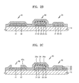
- FIG. 1 is a cross-sectional view of an organic light-emitting display device according to an embodiment of the invention.
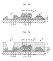
- FIGS. 2A through 2F are cross-sectional views of stages in a method of manufacturing an organic light-emitting display device according to an embodiment of the invention.
- an organic light-emitting display device includes a thin film transistor (TFT) 30, a capacitor 20, and an organic light-emitting device 40 on a substrate 10.
- TFT thin film transistor
- FIG. 1 illustrates only a single pixel of the organic light-emitting display device, but the organic light-emitting display device includes a plurality of the pixels.
- the organic light-emitting device 40 which is electrically connected to the TFT 30 and the capacitor 20, emits light.
- the organic light-emitting device 40 includes pixel electrodes 41 and 42 that are included in each pixel, an opposite electrode 44 which is a common electrode, and an organic emission layer 43 interposed between the pixel electrode 41 and the opposite electrode 44.
- a voltage is applied to the pixel electrodes 41 and 42 from the TFT 30 and the capacitor 20, i.e., a proper voltage condition is formed between the pixel electrodes 41 and 42 and the opposite electrode 44, the organic emission layer 43 emits light.
- the pixel electrode 41 may be a transparent electrode layer formed of, e.g., indium tin oxide (ITO), indium zinc oxide (IZO), or zinc oxide (ZnO), and the pixel electrode 42 may be a low resistance electrode layer formed of, e.g., molybdenum (Mo).
- ITO indium tin oxide
- IZO indium zinc oxide
- ZnO zinc oxide
- Mo molybdenum
- the pixel electrodes 41 and 42 may partially form a multi-layered structure.
- the opposite electrode 44 may include a semi-permeable reflecting layer formed of, e.g., Ag, Mg, Al, Pt, Pd, Au, Ni, Nd, Ir, Cr, Li, and/or Ca in a thin film type layer, or may include a light-transmissive metal oxide formed of, e.g., ITO, IZO, or ZnO.
- a semi-permeable reflecting layer formed of, e.g., Ag, Mg, Al, Pt, Pd, Au, Ni, Nd, Ir, Cr, Li, and/or Ca in a thin film type layer
- a light-transmissive metal oxide formed of, e.g., ITO, IZO, or ZnO.
- the organic emission layer 43 interposed between the pixel electrodes 41 and 42 and the opposite electrode 44 may have a stacked structure in which an emitting layer (EML) and at least one of a hole injection layer (HIL), a hole transport layer (HTL), an electron injection layer (EIL), an electron transport layer (ETL), etc. are stacked.
- EML emitting layer
- HIL hole injection layer
- HTL hole transport layer
- EIL electron injection layer
- ETL electron transport layer
- a protection layer may further be formed on the opposite electrode 44. Further, the organic light-emitting display device may be sealed, e.g., by glass.
- Reference numeral 50 denotes a pixel-defining layer.
- the organic emission layer 43 and the opposite electrode 44 may be formed on the pixel electrode 41 that is exposed by etching the pixel-defining layer 50.
- the TFT 30 includes gate electrodes 31 and 32 formed on the substrate 10, a second insulating layer 33 (or a gate insulating layer) covering the gate electrodes 31 and 32, an active layer 34 formed on the second insulating layer 33, a third insulating layer 35 (or an etching stop layer) covering the active layer 34, and the source and drain electrodes 36 and 37.
- Each of the source and drain electrodes 36 and 37 is connected to the active layer 34 via an aperture 35a of the third insulating layer 35.
- a buffer layer (not shown) may further be formed on the substrate 10.
- the buffer layer may be formed of an inorganic material, e.g., silicon oxide.
- the gate electrodes 31 and 32 may be formed as a single layer or a plurality of layers on the substrate 10.
- the gate electrodes 31 and 32 may be formed as a multi layer similar to the pixel electrodes 41 and 42, wherein the gate electrode 31 may be a transparent electrode layer and the gate electrode 32 may be a low resistance electrode layer.
- the second insulating layer 33 may be formed of, e.g., silicon oxide, tantalum oxide, and/or aluminum oxide. However, example embodiments are not limited thereto.
- the active layer 34 is formed on the second insulating layer 33.
- the active layer 34 may be formed of an oxide semiconductor, e.g., a G-I-Z-O layer [a(In 2 O 3 ) b(Ga 2 O 3 )c(ZnO) layer], wherein a, b, and c are real numbers satisfying the conditions of a ⁇ 0, b ⁇ 0, and c>0, respectively.
- the active layer 34 may be a Hf-In-Zn-O layer.
- the third insulating layer 35 covering the active layer 34 may be formed of, e.g., silicon oxide, tantalum oxide, and/or aluminum oxide. However, example embodiments are not limited thereto.
- the source and drain electrodes 36 and 37 are formed on the third insulating layer 35 to contact the active layer 34 via the apertures 35a.
- the drain electrode 37 is connected to the pixel electrode 42.
- the capacitor 20 includes first electrode layers 21 and 22, a first insulating layer 25, and second electrode layer 26 that are sequentially stacked on the substrate 10.
- the first electrode layers 21 and 22 are formed of the same layers as the above-described gate electrodes 31 and 32 of the TFT 30, respectively.
- the first electrode layers 21 and 22 may be formed as a multi layer structure, i.e., the first electrode 21 may be a transparent electrode layer and the first electrode 22 may be a low resistance electrode layer, similar to the respective gate electrodes 31 and 32.
- the first insulating layer 25 is formed of the same layer as the third insulating layer 35 of the TFT 30.
- the second electrode layer 26 is formed of the same layer as the source and drain electrodes 36 of the TFT 30. Further, the second electrode layer 26 is formed of a conductive metal material that is the same material for forming the source and drain electrodes 36 and 37.
- the capacity of the capacitor 20 may be increased. That is, since the capacity of the capacitor 20 is inversely proportional to a distance between an uppermost surface of the first electrode layers 21 and 22, i.e., an uppermost surface of the first electrode layer 22, and the second electrode layer 26, a decreased distance between the uppermost surface of the first electrode layers 21 and 22 and the second electrode layer 26 may increase the capacity of the capacitor 20.
- the organic light-emitting display device having the above-described structure only the first insulating layer 25 is interposed between the first electrode layers 21 and 22 and the second electrode layer 26, and thus, a high capacity of the capacitor 20 can be easily secured. Also, as will be described in a method of manufacturing the organic light-emitting display device of FIG. 1 , a structure in which only the first insulating layer 25 is interposed between the first electrode layers 21 and 22 and the second electrode layer 26 is naturally formed in a process of forming each layer constituting the organic light-emitting device 40, the TFT 30, and the capacitor 20, and thus, there is no need to perform an additional mask process.
- FIGS. 2A through 2F are cross-sectional views for sequentially describing a method of manufacturing the organic light-emitting display device of FIG. 1 .
- the first electrode layers 21 and 22 of the capacitor 20, the gate electrodes 31 and 32 of TFT 30, and the pixel electrodes 41 and 42 of the organic light-emitting device 40 are formed on the substrate 10. That is, the first electrode layer 21, the gate electrode 31, and the pixel electrode 41, which are transparent electrode layers, are formed, e.g., patterned, of a same first layer on, e.g., directly on, the substrate 10. Next, the first electrode layer 22, the gate electrode 32, and the pixel electrode 42, which are low resistance electrode layers, are formed, e.g., patterned, of a same second layer on, e.g., directly on, the first layer. Although not shown in FIG.
- a buffer layer may further be formed on the substrate 10.
- the electrode layer 21, gate electrode 31, and pixel electrode 41 are formed of a same layer, they are formed simultaneously to a substantially same thickness, as measured from the substrate 10.
- the first electrode layer 22, gate electrode 32, and pixel electrode 42 are formed of a same layer, they are formed simultaneously to a substantially same thickness, as measured from the substrate 10.
- Each of the first electrode layer 22, gate electrode 32, and pixel electrode 42 overlaps, e.g., completely overlaps, a respective one of the electrode layer 21, gate electrode 31, and pixel electrode 41.
- the second insulating layer 33 covering the gate electrodes 31 and 32 of the TFT 30 is formed, followed by forming the active layer 34 on the second insulating layer 33.
- an additional insulation layer is formed to cover the resultant structure, i.e., the pixel electrode 42, active layer 34, and first electrode 22.
- the additional insulation layer is a single layer having a first portion on the first electrode 22, i.e., first insulating layer 25, and a second portion on the pixel electrode 42 and active layer 34, i.3., third insulating layer 35.
- the first and third insulating layers 25 and 35 define a single continuous insulation layer overlapping the organic light-emitting device 40, the TFT 30, and the capacitor 20.
- the apertures 35a and 42a are formed in the third insulating layer 35, as illustrated in FIG. 2C .
- the second electrode layer 26 of the capacitor 20 and the source and drain electrodes 36 and 37 of the TFT 30 are formed, as illustrated in FIG. 2D .
- the source electrode 36 is connected to the active layer 34 via the aperture 35a
- the drain electrode 37 is connected to the active layer 34 and the pixel electrode 42 respectively via the aperture 35a and the aperture 42a.
- the source and drain electrodes 36 and 37 are patterned, a part of the pixel electrode 42 is etched, and thus, the pixel electrodes 41 and 42 may partially form a multi-layered structure.
- a basic structure of the capacitor 20 is completed, and thus, a stacked structure in which the first electrode layers 21 and 22, the first insulating layer 25, and the second electrode layer 26 are sequentially stacked is formed, as illustrated in FIG. 2D .
- the stacked structure in which an electrode layer, an insulating layer, and an electrode layer are sequentially stacked may increase the capacity of the capacitor 20.
- a conventional capacitor having a stacked structure may include a plurality of insulating layers between the first and second electrode layers, thereby decreasing capacity.
- the capacitor 20 according to an embodiment of the invention includes a single insulating layer that is formed as a single layer between two electrode layers, a total thickness of the insulating layer can be relatively decreased, thereby increasing the capacity of a capacitor.
- the first insulating layer 25 can be formed at the same time as the third insulating layer 35 of the TFT 30, a number of manufacturing processes may be decreased, thereby reducing manufacturing costs.
- the pixel-defining layer 50 is formed, followed by etching of the pixel-defining layer 50 to expose a part of the pixel electrode 41.
- the organic emission layer 43 is formed on the exposed pixel electrode 41, followed by formation of the opposite electrode 44 on the organic emission layer 43 to complete the manufacturing of the organic light-emitting display device, as illustrated in FIG. 2F .
- a protection layer may further be formed on the organic light-emitting display device, and the organic light-emitting display device may be sealed with glass.
- the capacity of the capacitor 20 may be increased without increasing the size of the capacitor 20. That is, the capacity of the capacitor 20 may be increased without reducing the size of an emission area of an organic light-emitting device. As such, the organic light-emitting device may display an image more stably and naturally.
Applications Claiming Priority (1)
| Application Number | Priority Date | Filing Date | Title |
|---|---|---|---|
| KR1020110022449A KR101781532B1 (ko) | 2011-03-14 | 2011-03-14 | 유기 발광 표시 장치와 그 제조방법 |
Publications (3)
| Publication Number | Publication Date |
|---|---|
| EP2500946A2 true EP2500946A2 (de) | 2012-09-19 |
| EP2500946A3 EP2500946A3 (de) | 2014-03-05 |
| EP2500946B1 EP2500946B1 (de) | 2017-01-04 |
Family
ID=45952852
Family Applications (1)
| Application Number | Title | Priority Date | Filing Date |
|---|---|---|---|
| EP12159126.7A Active EP2500946B1 (de) | 2011-03-14 | 2012-03-12 | Organische lichtemittierende Anzeige und Verfahren zu ihrer Herstellung |
Country Status (6)
| Country | Link |
|---|---|
| US (1) | US8901563B2 (de) |
| EP (1) | EP2500946B1 (de) |
| JP (1) | JP5964591B2 (de) |
| KR (1) | KR101781532B1 (de) |
| CN (1) | CN102683382B (de) |
| TW (1) | TWI555191B (de) |
Cited By (2)
| Publication number | Priority date | Publication date | Assignee | Title |
|---|---|---|---|---|
| WO2014049054A1 (de) * | 2012-09-28 | 2014-04-03 | Osram Opto Semiconductors Gmbh | Verfahren zum herstellen einer optoelektronischen baugruppe und optoelektronische baugruppe |
| EP3340301A1 (de) * | 2016-12-20 | 2018-06-27 | LG Display Co., Ltd. | Substrat für eine anzeigevorrichtung und anzeigevorrichtung damit |
Families Citing this family (12)
| Publication number | Priority date | Publication date | Assignee | Title |
|---|---|---|---|---|
| KR20120128966A (ko) * | 2011-05-18 | 2012-11-28 | 삼성디스플레이 주식회사 | 유기 발광 표시 장치 및 유기 발광 표시 장치 제조 방법 |
| CN103824862B (zh) * | 2012-11-16 | 2016-12-07 | 群康科技(深圳)有限公司 | 薄膜晶体管基板与显示器 |
| KR101548304B1 (ko) * | 2013-04-23 | 2015-08-28 | 엘지디스플레이 주식회사 | 유기 전계 발광 표시장치 및 그 제조방법 |
| KR102116493B1 (ko) * | 2013-05-23 | 2020-06-08 | 삼성디스플레이 주식회사 | 유기발광표시장치 및 이의 제조방법 |
| KR20150135722A (ko) * | 2014-05-23 | 2015-12-03 | 삼성디스플레이 주식회사 | 유기발광 디스플레이 장치 및 그 제조방법 |
| KR102396288B1 (ko) | 2014-10-27 | 2022-05-10 | 삼성디스플레이 주식회사 | 유기 발광 표시 장치 |
| KR102346675B1 (ko) * | 2014-10-31 | 2022-01-04 | 삼성디스플레이 주식회사 | 디스플레이 장치 및 그 제조 방법 |
| KR102293123B1 (ko) * | 2015-04-08 | 2021-08-24 | 삼성디스플레이 주식회사 | 박막 트랜지스터, 유기 발광 표시 장치, 유기 발광 표시 장치의 제조 방법 |
| KR102433316B1 (ko) | 2015-08-06 | 2022-08-17 | 삼성디스플레이 주식회사 | 유기 발광 표시 장치 |
| CN207165572U (zh) * | 2017-09-12 | 2018-03-30 | 京东方科技集团股份有限公司 | 一种阵列基板及显示装置 |
| CN109659445A (zh) * | 2018-12-19 | 2019-04-19 | 武汉华星光电半导体显示技术有限公司 | 显示面板及其显示屏 |
| TWI677979B (zh) * | 2019-03-21 | 2019-11-21 | 友達光電股份有限公司 | 顯示面板及其製作方法 |
Family Cites Families (22)
| Publication number | Priority date | Publication date | Assignee | Title |
|---|---|---|---|---|
| JP2682997B2 (ja) * | 1987-11-14 | 1997-11-26 | 株式会社日立製作所 | 補助容量付液晶表示装置及び補助容量付液晶表示装置の製造方法 |
| JP2001255543A (ja) * | 2000-03-10 | 2001-09-21 | Hitachi Ltd | 液晶表示装置 |
| JP2002229065A (ja) * | 2001-02-07 | 2002-08-14 | Hitachi Ltd | 液晶表示装置とその製造方法 |
| KR100669733B1 (ko) * | 2004-10-14 | 2007-01-16 | 삼성에스디아이 주식회사 | 유기박막 트랜지스터 및 이를 이용한 유기전계 발광표시장치 |
| KR100683685B1 (ko) | 2004-10-28 | 2007-02-15 | 삼성에스디아이 주식회사 | 유기박막 트랜지스터를 구비한 유기전계 발광표시장치 및그의 제조방법 |
| US7812893B2 (en) * | 2004-11-17 | 2010-10-12 | Sharp Kabushiki Kaisha | Active matrix substrate where a portion of the storage capacitor wiring or the scanning signal line overlaps with the drain lead-out wiring connected to the drain electrode of a thin film transistor and display device having such an active matrix substrate |
| KR100700642B1 (ko) | 2004-12-13 | 2007-03-27 | 삼성에스디아이 주식회사 | 유기전계발광표시소자 및 그 제조방법 |
| TWI262743B (en) * | 2005-10-12 | 2006-09-21 | Au Optronics Corp | A controlling element of an organic electro-luminescent display and manufacturing process thereof |
| KR101277606B1 (ko) * | 2006-03-22 | 2013-06-21 | 삼성디스플레이 주식회사 | 표시 장치 및 그 제조 방법 |
| JP5508664B2 (ja) * | 2006-04-05 | 2014-06-04 | 株式会社半導体エネルギー研究所 | 半導体装置、表示装置及び電子機器 |
| JP2008129314A (ja) * | 2006-11-21 | 2008-06-05 | Hitachi Displays Ltd | 画像表示装置およびその製造方法 |
| JP5127300B2 (ja) * | 2007-05-28 | 2013-01-23 | キヤノン株式会社 | フルオレン化合物及びそれを用いた有機発光素子並びに表示装置 |
| KR100953654B1 (ko) * | 2008-06-26 | 2010-04-20 | 삼성모바일디스플레이주식회사 | 유기 발광 표시 장치 및 그 제조 방법 |
| KR100963104B1 (ko) * | 2008-07-08 | 2010-06-14 | 삼성모바일디스플레이주식회사 | 박막 트랜지스터, 그의 제조 방법 및 박막 트랜지스터를구비하는 평판 표시 장치 |
| KR101148829B1 (ko) | 2008-10-23 | 2012-05-29 | 삼성전자주식회사 | 박막 트랜지스터 |
| KR101546425B1 (ko) | 2008-12-22 | 2015-08-24 | 엘지디스플레이 주식회사 | 전기영동 표시장치 및 그 제조 방법 |
| KR101074788B1 (ko) * | 2009-01-30 | 2011-10-20 | 삼성모바일디스플레이주식회사 | 평판 표시 장치 및 이의 제조 방법 |
| KR101041141B1 (ko) * | 2009-03-03 | 2011-06-13 | 삼성모바일디스플레이주식회사 | 유기전계발광표시장치 및 그의 제조방법 |
| KR101127574B1 (ko) * | 2009-04-06 | 2012-03-23 | 삼성모바일디스플레이주식회사 | 액티브 매트릭스 기판의 제조방법 및 유기 발광 표시장치의 제조방법 |
| KR101050461B1 (ko) * | 2009-04-23 | 2011-07-19 | 삼성모바일디스플레이주식회사 | 유기 발광 디스플레이 장치 및 유기 발광 디스플레이 장치의 제조방법 |
| KR101857405B1 (ko) * | 2009-07-10 | 2018-05-11 | 가부시키가이샤 한도오따이 에네루기 켄큐쇼 | 반도체 장치 및 그 제조 방법 |
| KR101093424B1 (ko) * | 2009-11-10 | 2011-12-14 | 삼성모바일디스플레이주식회사 | 유기전계발광 표시 장치 및 그의 제조 방법 |
-
2011
- 2011-03-14 KR KR1020110022449A patent/KR101781532B1/ko active IP Right Grant
-
2012
- 2012-01-11 JP JP2012003162A patent/JP5964591B2/ja active Active
- 2012-01-24 US US13/356,923 patent/US8901563B2/en active Active
- 2012-01-31 TW TW101103043A patent/TWI555191B/zh active
- 2012-02-10 CN CN201210030495.3A patent/CN102683382B/zh active Active
- 2012-03-12 EP EP12159126.7A patent/EP2500946B1/de active Active
Non-Patent Citations (1)
| Title |
|---|
| None |
Cited By (5)
| Publication number | Priority date | Publication date | Assignee | Title |
|---|---|---|---|---|
| WO2014049054A1 (de) * | 2012-09-28 | 2014-04-03 | Osram Opto Semiconductors Gmbh | Verfahren zum herstellen einer optoelektronischen baugruppe und optoelektronische baugruppe |
| US9553133B2 (en) | 2012-09-28 | 2017-01-24 | Osram Oled Gmbh | Method for producing an optoelectronic assembly, and optoelectronic assembly |
| EP3340301A1 (de) * | 2016-12-20 | 2018-06-27 | LG Display Co., Ltd. | Substrat für eine anzeigevorrichtung und anzeigevorrichtung damit |
| US10340320B2 (en) | 2016-12-20 | 2019-07-02 | Lg Display Co., Ltd. | Substrate for display device and display device including the same |
| US10714557B2 (en) | 2016-12-20 | 2020-07-14 | Lg Display Co., Ltd. | Substrate for display device and display device including the same |
Also Published As
| Publication number | Publication date |
|---|---|
| EP2500946B1 (de) | 2017-01-04 |
| US20120235147A1 (en) | 2012-09-20 |
| KR20120104816A (ko) | 2012-09-24 |
| US8901563B2 (en) | 2014-12-02 |
| CN102683382A (zh) | 2012-09-19 |
| TWI555191B (zh) | 2016-10-21 |
| EP2500946A3 (de) | 2014-03-05 |
| CN102683382B (zh) | 2016-05-04 |
| JP2012195283A (ja) | 2012-10-11 |
| TW201238045A (en) | 2012-09-16 |
| JP5964591B2 (ja) | 2016-08-03 |
| KR101781532B1 (ko) | 2017-10-24 |
Similar Documents
| Publication | Publication Date | Title |
|---|---|---|
| EP2500946B1 (de) | Organische lichtemittierende Anzeige und Verfahren zu ihrer Herstellung | |
| KR102124025B1 (ko) | 유기발광다이오드 표시장치 및 그 제조방법 | |
| US9570527B2 (en) | Organic light emitting diode display | |
| US9425426B2 (en) | Organic light emitting diode display having auxiliary electrode | |
| KR101961190B1 (ko) | 유기전압 발광소자 및 이의 제조방법 | |
| US9893312B2 (en) | Display device and organic luminescent display device | |
| US8367448B2 (en) | Capacitor and organic light emitting display device | |
| US20170005158A1 (en) | Organic Light Emitting Diode Display Device and Method of Fabricating the Same | |
| US9941341B2 (en) | Transparent display apparatus | |
| US9859349B2 (en) | Organic electroluminescent display substrate and manufacturing method thereof, and display device | |
| KR102575459B1 (ko) | 유기발광 표시장치 및 이의 제조방법 | |
| US10937838B2 (en) | Organic light emitting display device | |
| US9349996B2 (en) | Method of manufacturing capacitor, method of manufacturing organic light emitting display device including the capacitor, and organic light emitting display device manufactured by using the method | |
| US9299759B2 (en) | Organic light-emitting display device and method of manufacturing the same | |
| CN106997893B (zh) | 有机发光显示装置及其制造方法 | |
| US9859351B2 (en) | Organic light-emitting diode display | |
| US20150171153A1 (en) | Organic light emitting display device | |
| KR102077723B1 (ko) | 유기발광표시장치 및 그 제조방법 | |
| KR20160058297A (ko) | 유기발광다이오드 표시장치 및 그 제조방법 | |
| US9029865B2 (en) | Organic light emitting diode display and method for manufacturing the same | |
| KR102317821B1 (ko) | 유기발광소자 | |
| JP2015141808A (ja) | 有機電界発光装置および電子機器 |
Legal Events
| Date | Code | Title | Description |
|---|---|---|---|
| PUAI | Public reference made under article 153(3) epc to a published international application that has entered the european phase |
Free format text: ORIGINAL CODE: 0009012 |
|
| AK | Designated contracting states |
Kind code of ref document: A2 Designated state(s): AL AT BE BG CH CY CZ DE DK EE ES FI FR GB GR HR HU IE IS IT LI LT LU LV MC MK MT NL NO PL PT RO RS SE SI SK SM TR |
|
| AX | Request for extension of the european patent |
Extension state: BA ME |
|
| RAP1 | Party data changed (applicant data changed or rights of an application transferred) |
Owner name: SAMSUNG DISPLAY CO., LTD. |
|
| PUAL | Search report despatched |
Free format text: ORIGINAL CODE: 0009013 |
|
| AK | Designated contracting states |
Kind code of ref document: A3 Designated state(s): AL AT BE BG CH CY CZ DE DK EE ES FI FR GB GR HR HU IE IS IT LI LT LU LV MC MK MT NL NO PL PT RO RS SE SI SK SM TR |
|
| AX | Request for extension of the european patent |
Extension state: BA ME |
|
| RIC1 | Information provided on ipc code assigned before grant |
Ipc: H01L 51/52 20060101ALI20140128BHEP Ipc: H01L 27/12 20060101ALI20140128BHEP Ipc: H01L 27/32 20060101AFI20140128BHEP |
|
| 17P | Request for examination filed |
Effective date: 20140321 |
|
| RBV | Designated contracting states (corrected) |
Designated state(s): AL AT BE BG CH CY CZ DE DK EE ES FI FR GB GR HR HU IE IS IT LI LT LU LV MC MK MT NL NO PL PT RO RS SE SI SK SM TR |
|
| RAP1 | Party data changed (applicant data changed or rights of an application transferred) |
Owner name: SAMSUNG DISPLAY CO., LTD. |
|
| GRAP | Despatch of communication of intention to grant a patent |
Free format text: ORIGINAL CODE: EPIDOSNIGR1 |
|
| INTG | Intention to grant announced |
Effective date: 20160712 |
|
| GRAS | Grant fee paid |
Free format text: ORIGINAL CODE: EPIDOSNIGR3 |
|
| GRAA | (expected) grant |
Free format text: ORIGINAL CODE: 0009210 |
|
| AK | Designated contracting states |
Kind code of ref document: B1 Designated state(s): AL AT BE BG CH CY CZ DE DK EE ES FI FR GB GR HR HU IE IS IT LI LT LU LV MC MK MT NL NO PL PT RO RS SE SI SK SM TR |
|
| REG | Reference to a national code |
Ref country code: GB Ref legal event code: FG4D |
|
| REG | Reference to a national code |
Ref country code: CH Ref legal event code: EP |
|
| REG | Reference to a national code |
Ref country code: AT Ref legal event code: REF Ref document number: 860004 Country of ref document: AT Kind code of ref document: T Effective date: 20170115 |
|
| REG | Reference to a national code |
Ref country code: IE Ref legal event code: FG4D |
|
| REG | Reference to a national code |
Ref country code: DE Ref legal event code: R096 Ref document number: 602012027285 Country of ref document: DE |
|
| REG | Reference to a national code |
Ref country code: FR Ref legal event code: PLFP Year of fee payment: 6 |
|
| REG | Reference to a national code |
Ref country code: NL Ref legal event code: FP |
|
| REG | Reference to a national code |
Ref country code: LT Ref legal event code: MG4D |
|
| REG | Reference to a national code |
Ref country code: AT Ref legal event code: MK05 Ref document number: 860004 Country of ref document: AT Kind code of ref document: T Effective date: 20170104 |
|
| PG25 | Lapsed in a contracting state [announced via postgrant information from national office to epo] |
Ref country code: IS Free format text: LAPSE BECAUSE OF FAILURE TO SUBMIT A TRANSLATION OF THE DESCRIPTION OR TO PAY THE FEE WITHIN THE PRESCRIBED TIME-LIMIT Effective date: 20170504 Ref country code: HR Free format text: LAPSE BECAUSE OF FAILURE TO SUBMIT A TRANSLATION OF THE DESCRIPTION OR TO PAY THE FEE WITHIN THE PRESCRIBED TIME-LIMIT Effective date: 20170104 Ref country code: FI Free format text: LAPSE BECAUSE OF FAILURE TO SUBMIT A TRANSLATION OF THE DESCRIPTION OR TO PAY THE FEE WITHIN THE PRESCRIBED TIME-LIMIT Effective date: 20170104 Ref country code: LT Free format text: LAPSE BECAUSE OF FAILURE TO SUBMIT A TRANSLATION OF THE DESCRIPTION OR TO PAY THE FEE WITHIN THE PRESCRIBED TIME-LIMIT Effective date: 20170104 Ref country code: GR Free format text: LAPSE BECAUSE OF FAILURE TO SUBMIT A TRANSLATION OF THE DESCRIPTION OR TO PAY THE FEE WITHIN THE PRESCRIBED TIME-LIMIT Effective date: 20170405 Ref country code: NO Free format text: LAPSE BECAUSE OF FAILURE TO SUBMIT A TRANSLATION OF THE DESCRIPTION OR TO PAY THE FEE WITHIN THE PRESCRIBED TIME-LIMIT Effective date: 20170404 |
|
| PG25 | Lapsed in a contracting state [announced via postgrant information from national office to epo] |
Ref country code: SE Free format text: LAPSE BECAUSE OF FAILURE TO SUBMIT A TRANSLATION OF THE DESCRIPTION OR TO PAY THE FEE WITHIN THE PRESCRIBED TIME-LIMIT Effective date: 20170104 Ref country code: BG Free format text: LAPSE BECAUSE OF FAILURE TO SUBMIT A TRANSLATION OF THE DESCRIPTION OR TO PAY THE FEE WITHIN THE PRESCRIBED TIME-LIMIT Effective date: 20170404 Ref country code: ES Free format text: LAPSE BECAUSE OF FAILURE TO SUBMIT A TRANSLATION OF THE DESCRIPTION OR TO PAY THE FEE WITHIN THE PRESCRIBED TIME-LIMIT Effective date: 20170104 Ref country code: PL Free format text: LAPSE BECAUSE OF FAILURE TO SUBMIT A TRANSLATION OF THE DESCRIPTION OR TO PAY THE FEE WITHIN THE PRESCRIBED TIME-LIMIT Effective date: 20170104 Ref country code: LV Free format text: LAPSE BECAUSE OF FAILURE TO SUBMIT A TRANSLATION OF THE DESCRIPTION OR TO PAY THE FEE WITHIN THE PRESCRIBED TIME-LIMIT Effective date: 20170104 Ref country code: PT Free format text: LAPSE BECAUSE OF FAILURE TO SUBMIT A TRANSLATION OF THE DESCRIPTION OR TO PAY THE FEE WITHIN THE PRESCRIBED TIME-LIMIT Effective date: 20170504 Ref country code: RS Free format text: LAPSE BECAUSE OF FAILURE TO SUBMIT A TRANSLATION OF THE DESCRIPTION OR TO PAY THE FEE WITHIN THE PRESCRIBED TIME-LIMIT Effective date: 20170104 Ref country code: AT Free format text: LAPSE BECAUSE OF FAILURE TO SUBMIT A TRANSLATION OF THE DESCRIPTION OR TO PAY THE FEE WITHIN THE PRESCRIBED TIME-LIMIT Effective date: 20170104 |
|
| REG | Reference to a national code |
Ref country code: DE Ref legal event code: R097 Ref document number: 602012027285 Country of ref document: DE |
|
| PG25 | Lapsed in a contracting state [announced via postgrant information from national office to epo] |
Ref country code: SK Free format text: LAPSE BECAUSE OF FAILURE TO SUBMIT A TRANSLATION OF THE DESCRIPTION OR TO PAY THE FEE WITHIN THE PRESCRIBED TIME-LIMIT Effective date: 20170104 Ref country code: EE Free format text: LAPSE BECAUSE OF FAILURE TO SUBMIT A TRANSLATION OF THE DESCRIPTION OR TO PAY THE FEE WITHIN THE PRESCRIBED TIME-LIMIT Effective date: 20170104 Ref country code: RO Free format text: LAPSE BECAUSE OF FAILURE TO SUBMIT A TRANSLATION OF THE DESCRIPTION OR TO PAY THE FEE WITHIN THE PRESCRIBED TIME-LIMIT Effective date: 20170104 Ref country code: CZ Free format text: LAPSE BECAUSE OF FAILURE TO SUBMIT A TRANSLATION OF THE DESCRIPTION OR TO PAY THE FEE WITHIN THE PRESCRIBED TIME-LIMIT Effective date: 20170104 Ref country code: IT Free format text: LAPSE BECAUSE OF FAILURE TO SUBMIT A TRANSLATION OF THE DESCRIPTION OR TO PAY THE FEE WITHIN THE PRESCRIBED TIME-LIMIT Effective date: 20170104 |
|
| REG | Reference to a national code |
Ref country code: CH Ref legal event code: PL |
|
| PLBE | No opposition filed within time limit |
Free format text: ORIGINAL CODE: 0009261 |
|
| STAA | Information on the status of an ep patent application or granted ep patent |
Free format text: STATUS: NO OPPOSITION FILED WITHIN TIME LIMIT |
|
| PG25 | Lapsed in a contracting state [announced via postgrant information from national office to epo] |
Ref country code: MC Free format text: LAPSE BECAUSE OF FAILURE TO SUBMIT A TRANSLATION OF THE DESCRIPTION OR TO PAY THE FEE WITHIN THE PRESCRIBED TIME-LIMIT Effective date: 20170104 Ref country code: SM Free format text: LAPSE BECAUSE OF FAILURE TO SUBMIT A TRANSLATION OF THE DESCRIPTION OR TO PAY THE FEE WITHIN THE PRESCRIBED TIME-LIMIT Effective date: 20170104 Ref country code: DK Free format text: LAPSE BECAUSE OF FAILURE TO SUBMIT A TRANSLATION OF THE DESCRIPTION OR TO PAY THE FEE WITHIN THE PRESCRIBED TIME-LIMIT Effective date: 20170104 |
|
| 26N | No opposition filed |
Effective date: 20171005 |
|
| REG | Reference to a national code |
Ref country code: IE Ref legal event code: MM4A |
|
| PG25 | Lapsed in a contracting state [announced via postgrant information from national office to epo] |
Ref country code: LU Free format text: LAPSE BECAUSE OF NON-PAYMENT OF DUE FEES Effective date: 20170312 |
|
| REG | Reference to a national code |
Ref country code: FR Ref legal event code: PLFP Year of fee payment: 7 |
|
| PG25 | Lapsed in a contracting state [announced via postgrant information from national office to epo] |
Ref country code: IE Free format text: LAPSE BECAUSE OF NON-PAYMENT OF DUE FEES Effective date: 20170312 Ref country code: LI Free format text: LAPSE BECAUSE OF NON-PAYMENT OF DUE FEES Effective date: 20170331 Ref country code: CH Free format text: LAPSE BECAUSE OF NON-PAYMENT OF DUE FEES Effective date: 20170331 Ref country code: SI Free format text: LAPSE BECAUSE OF FAILURE TO SUBMIT A TRANSLATION OF THE DESCRIPTION OR TO PAY THE FEE WITHIN THE PRESCRIBED TIME-LIMIT Effective date: 20170104 |
|
| REG | Reference to a national code |
Ref country code: BE Ref legal event code: MM Effective date: 20170331 |
|
| PG25 | Lapsed in a contracting state [announced via postgrant information from national office to epo] |
Ref country code: BE Free format text: LAPSE BECAUSE OF NON-PAYMENT OF DUE FEES Effective date: 20170331 |
|
| PG25 | Lapsed in a contracting state [announced via postgrant information from national office to epo] |
Ref country code: MT Free format text: LAPSE BECAUSE OF NON-PAYMENT OF DUE FEES Effective date: 20170312 |
|
| PG25 | Lapsed in a contracting state [announced via postgrant information from national office to epo] |
Ref country code: HU Free format text: LAPSE BECAUSE OF FAILURE TO SUBMIT A TRANSLATION OF THE DESCRIPTION OR TO PAY THE FEE WITHIN THE PRESCRIBED TIME-LIMIT; INVALID AB INITIO Effective date: 20120312 |
|
| PG25 | Lapsed in a contracting state [announced via postgrant information from national office to epo] |
Ref country code: CY Free format text: LAPSE BECAUSE OF NON-PAYMENT OF DUE FEES Effective date: 20170104 |
|
| PG25 | Lapsed in a contracting state [announced via postgrant information from national office to epo] |
Ref country code: MK Free format text: LAPSE BECAUSE OF FAILURE TO SUBMIT A TRANSLATION OF THE DESCRIPTION OR TO PAY THE FEE WITHIN THE PRESCRIBED TIME-LIMIT Effective date: 20170104 |
|
| PG25 | Lapsed in a contracting state [announced via postgrant information from national office to epo] |
Ref country code: TR Free format text: LAPSE BECAUSE OF FAILURE TO SUBMIT A TRANSLATION OF THE DESCRIPTION OR TO PAY THE FEE WITHIN THE PRESCRIBED TIME-LIMIT Effective date: 20170104 |
|
| PG25 | Lapsed in a contracting state [announced via postgrant information from national office to epo] |
Ref country code: AL Free format text: LAPSE BECAUSE OF FAILURE TO SUBMIT A TRANSLATION OF THE DESCRIPTION OR TO PAY THE FEE WITHIN THE PRESCRIBED TIME-LIMIT Effective date: 20170104 |
|
| REG | Reference to a national code |
Ref country code: DE Ref legal event code: R079 Ref document number: 602012027285 Country of ref document: DE Free format text: PREVIOUS MAIN CLASS: H01L0027320000 Ipc: H10K0059000000 |
|
| PGFP | Annual fee paid to national office [announced via postgrant information from national office to epo] |
Ref country code: NL Payment date: 20230221 Year of fee payment: 12 |
|
| PGFP | Annual fee paid to national office [announced via postgrant information from national office to epo] |
Ref country code: FR Payment date: 20230221 Year of fee payment: 12 |
|
| P01 | Opt-out of the competence of the unified patent court (upc) registered |
Effective date: 20230515 |
|
| PGFP | Annual fee paid to national office [announced via postgrant information from national office to epo] |
Ref country code: NL Payment date: 20240221 Year of fee payment: 13 |
|
| PGFP | Annual fee paid to national office [announced via postgrant information from national office to epo] |
Ref country code: DE Payment date: 20240220 Year of fee payment: 13 Ref country code: GB Payment date: 20240220 Year of fee payment: 13 |