EP2496661B1 - Transparente leitende beschichtungen für optoelelektronische und elektronische bauelemente - Google Patents
Transparente leitende beschichtungen für optoelelektronische und elektronische bauelemente Download PDFInfo
- Publication number
- EP2496661B1 EP2496661B1 EP10790862.6A EP10790862A EP2496661B1 EP 2496661 B1 EP2496661 B1 EP 2496661B1 EP 10790862 A EP10790862 A EP 10790862A EP 2496661 B1 EP2496661 B1 EP 2496661B1
- Authority
- EP
- European Patent Office
- Prior art keywords
- conductive
- substrate
- film
- microns
- ring
- Prior art date
- Legal status (The legal status is an assumption and is not a legal conclusion. Google has not performed a legal analysis and makes no representation as to the accuracy of the status listed.)
- Not-in-force
Links
- 238000000576 coating method Methods 0.000 title claims description 20
- 230000005693 optoelectronics Effects 0.000 title description 7
- 239000000463 material Substances 0.000 claims description 102
- 239000000758 substrate Substances 0.000 claims description 81
- 239000004020 conductor Substances 0.000 claims description 67
- 238000000034 method Methods 0.000 claims description 40
- 230000008569 process Effects 0.000 claims description 29
- 239000004065 semiconductor Substances 0.000 claims description 23
- 239000011800 void material Substances 0.000 claims description 16
- 229910052751 metal Inorganic materials 0.000 claims description 15
- 239000002184 metal Substances 0.000 claims description 15
- -1 poly(3,4-dioctyloxythiophene) Polymers 0.000 claims description 14
- 239000011248 coating agent Substances 0.000 claims description 12
- 239000000203 mixture Substances 0.000 claims description 10
- 239000003575 carbonaceous material Substances 0.000 claims description 9
- 239000002243 precursor Substances 0.000 claims description 9
- 229920001940 conductive polymer Polymers 0.000 claims description 8
- 238000004519 manufacturing process Methods 0.000 claims description 8
- 150000002739 metals Chemical class 0.000 claims description 7
- WUPHOULIZUERAE-UHFFFAOYSA-N 3-(oxolan-2-yl)propanoic acid Chemical compound OC(=O)CCC1CCCO1 WUPHOULIZUERAE-UHFFFAOYSA-N 0.000 claims description 6
- MARUHZGHZWCEQU-UHFFFAOYSA-N 5-phenyl-2h-tetrazole Chemical compound C1=CC=CC=C1C1=NNN=N1 MARUHZGHZWCEQU-UHFFFAOYSA-N 0.000 claims description 6
- XUIMIQQOPSSXEZ-UHFFFAOYSA-N Silicon Chemical compound [Si] XUIMIQQOPSSXEZ-UHFFFAOYSA-N 0.000 claims description 6
- 229910052980 cadmium sulfide Inorganic materials 0.000 claims description 6
- 239000011521 glass Substances 0.000 claims description 6
- 239000002096 quantum dot Substances 0.000 claims description 6
- 229910052710 silicon Inorganic materials 0.000 claims description 6
- 239000010703 silicon Substances 0.000 claims description 6
- JBRZTFJDHDCESZ-UHFFFAOYSA-N AsGa Chemical compound [As]#[Ga] JBRZTFJDHDCESZ-UHFFFAOYSA-N 0.000 claims description 5
- 238000006073 displacement reaction Methods 0.000 claims description 5
- 229910052723 transition metal Inorganic materials 0.000 claims description 5
- 150000003624 transition metals Chemical class 0.000 claims description 5
- 229910000661 Mercury cadmium telluride Inorganic materials 0.000 claims description 4
- MDPILPRLPQYEEN-UHFFFAOYSA-N aluminium arsenide Chemical compound [As]#[Al] MDPILPRLPQYEEN-UHFFFAOYSA-N 0.000 claims description 4
- 229920001467 poly(styrenesulfonates) Polymers 0.000 claims description 4
- GYHNNYVSQQEPJS-UHFFFAOYSA-N Gallium Chemical compound [Ga] GYHNNYVSQQEPJS-UHFFFAOYSA-N 0.000 claims description 3
- 229910001218 Gallium arsenide Inorganic materials 0.000 claims description 3
- GPXJNWSHGFTCBW-UHFFFAOYSA-N Indium phosphide Chemical compound [In]#P GPXJNWSHGFTCBW-UHFFFAOYSA-N 0.000 claims description 3
- ATJFFYVFTNAWJD-UHFFFAOYSA-N Tin Chemical compound [Sn] ATJFFYVFTNAWJD-UHFFFAOYSA-N 0.000 claims description 3
- 229910045601 alloy Inorganic materials 0.000 claims description 3
- 239000000956 alloy Substances 0.000 claims description 3
- 229910052733 gallium Inorganic materials 0.000 claims description 3
- HZXMRANICFIONG-UHFFFAOYSA-N gallium phosphide Chemical compound [Ga]#P HZXMRANICFIONG-UHFFFAOYSA-N 0.000 claims description 3
- ZOXJGFHDIHLPTG-UHFFFAOYSA-N Boron Chemical compound [B] ZOXJGFHDIHLPTG-UHFFFAOYSA-N 0.000 claims description 2
- 241000208152 Geranium Species 0.000 claims description 2
- 229920001609 Poly(3,4-ethylenedioxythiophene) Polymers 0.000 claims description 2
- 239000004952 Polyamide Substances 0.000 claims description 2
- 239000004642 Polyimide Substances 0.000 claims description 2
- 229910052796 boron Inorganic materials 0.000 claims description 2
- MCMSPRNYOJJPIZ-UHFFFAOYSA-N cadmium;mercury;tellurium Chemical compound [Cd]=[Te]=[Hg] MCMSPRNYOJJPIZ-UHFFFAOYSA-N 0.000 claims description 2
- 150000001875 compounds Chemical class 0.000 claims description 2
- HVMJUDPAXRRVQO-UHFFFAOYSA-N copper indium Chemical compound [Cu].[In] HVMJUDPAXRRVQO-UHFFFAOYSA-N 0.000 claims description 2
- LCUOIYYHNRBAFS-UHFFFAOYSA-N copper;sulfanylideneindium Chemical compound [Cu].[In]=S LCUOIYYHNRBAFS-UHFFFAOYSA-N 0.000 claims description 2
- ZZEMEJKDTZOXOI-UHFFFAOYSA-N digallium;selenium(2-) Chemical compound [Ga+3].[Ga+3].[Se-2].[Se-2].[Se-2] ZZEMEJKDTZOXOI-UHFFFAOYSA-N 0.000 claims description 2
- 229920003229 poly(methyl methacrylate) Polymers 0.000 claims description 2
- 229920000058 polyacrylate Polymers 0.000 claims description 2
- 229920002647 polyamide Polymers 0.000 claims description 2
- 229920000767 polyaniline Polymers 0.000 claims description 2
- 239000004417 polycarbonate Substances 0.000 claims description 2
- 229920000515 polycarbonate Polymers 0.000 claims description 2
- 229920000728 polyester Polymers 0.000 claims description 2
- 229920001721 polyimide Polymers 0.000 claims description 2
- 239000004926 polymethyl methacrylate Substances 0.000 claims description 2
- 229920000098 polyolefin Polymers 0.000 claims description 2
- 229920000128 polypyrrole Polymers 0.000 claims description 2
- 229910052714 tellurium Inorganic materials 0.000 claims description 2
- PORWMNRCUJJQNO-UHFFFAOYSA-N tellurium atom Chemical compound [Te] PORWMNRCUJJQNO-UHFFFAOYSA-N 0.000 claims description 2
- KTSFMFGEAAANTF-UHFFFAOYSA-N [Cu].[Se].[Se].[In] Chemical compound [Cu].[Se].[Se].[In] KTSFMFGEAAANTF-UHFFFAOYSA-N 0.000 claims 1
- 229910010293 ceramic material Inorganic materials 0.000 claims 1
- 239000011147 inorganic material Substances 0.000 claims 1
- 239000011368 organic material Substances 0.000 claims 1
- 239000010408 film Substances 0.000 description 101
- 239000010410 layer Substances 0.000 description 28
- BQCADISMDOOEFD-UHFFFAOYSA-N Silver Chemical compound [Ag] BQCADISMDOOEFD-UHFFFAOYSA-N 0.000 description 21
- 229910052709 silver Inorganic materials 0.000 description 20
- 239000004332 silver Substances 0.000 description 19
- OKTJSMMVPCPJKN-UHFFFAOYSA-N Carbon Chemical compound [C] OKTJSMMVPCPJKN-UHFFFAOYSA-N 0.000 description 18
- 238000007639 printing Methods 0.000 description 18
- 239000002105 nanoparticle Substances 0.000 description 16
- 239000002245 particle Substances 0.000 description 16
- 230000015572 biosynthetic process Effects 0.000 description 15
- 239000002041 carbon nanotube Substances 0.000 description 13
- 229910021393 carbon nanotube Inorganic materials 0.000 description 13
- 239000006185 dispersion Substances 0.000 description 13
- 238000003491 array Methods 0.000 description 11
- 239000002904 solvent Substances 0.000 description 11
- 238000007641 inkjet printing Methods 0.000 description 10
- FOIXSVOLVBLSDH-UHFFFAOYSA-N Silver ion Chemical compound [Ag+] FOIXSVOLVBLSDH-UHFFFAOYSA-N 0.000 description 7
- 239000010949 copper Substances 0.000 description 7
- 239000007788 liquid Substances 0.000 description 7
- 238000005259 measurement Methods 0.000 description 7
- 229910021387 carbon allotrope Inorganic materials 0.000 description 6
- 239000006229 carbon black Substances 0.000 description 6
- 238000000151 deposition Methods 0.000 description 6
- 238000001704 evaporation Methods 0.000 description 6
- 230000008020 evaporation Effects 0.000 description 6
- 238000010438 heat treatment Methods 0.000 description 6
- 238000012856 packing Methods 0.000 description 6
- 239000007864 aqueous solution Substances 0.000 description 5
- 230000008021 deposition Effects 0.000 description 5
- 230000000694 effects Effects 0.000 description 5
- 230000033001 locomotion Effects 0.000 description 5
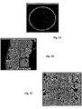
- 238000001878 scanning electron micrograph Methods 0.000 description 5
- 238000009736 wetting Methods 0.000 description 5
- 229920003023 plastic Polymers 0.000 description 4
- 239000004033 plastic Substances 0.000 description 4
- 238000002834 transmittance Methods 0.000 description 4
- 230000005540 biological transmission Effects 0.000 description 3
- 238000001124 conductive atomic force microscopy Methods 0.000 description 3
- 229910052802 copper Inorganic materials 0.000 description 3
- 238000007363 ring formation reaction Methods 0.000 description 3
- 238000001338 self-assembly Methods 0.000 description 3
- 238000005245 sintering Methods 0.000 description 3
- 239000000243 solution Substances 0.000 description 3
- 239000000126 substance Substances 0.000 description 3
- 239000010409 thin film Substances 0.000 description 3
- XLYOFNOQVPJJNP-UHFFFAOYSA-N water Substances O XLYOFNOQVPJJNP-UHFFFAOYSA-N 0.000 description 3
- XMWRBQBLMFGWIX-UHFFFAOYSA-N C60 fullerene Chemical class C12=C3C(C4=C56)=C7C8=C5C5=C9C%10=C6C6=C4C1=C1C4=C6C6=C%10C%10=C9C9=C%11C5=C8C5=C8C7=C3C3=C7C2=C1C1=C2C4=C6C4=C%10C6=C9C9=C%11C5=C5C8=C3C3=C7C1=C1C2=C4C6=C2C9=C5C3=C12 XMWRBQBLMFGWIX-UHFFFAOYSA-N 0.000 description 2
- 240000002329 Inga feuillei Species 0.000 description 2
- 238000005452 bending Methods 0.000 description 2
- YKYOUMDCQGMQQO-UHFFFAOYSA-L cadmium dichloride Chemical compound Cl[Cd]Cl YKYOUMDCQGMQQO-UHFFFAOYSA-L 0.000 description 2
- XIEPJMXMMWZAAV-UHFFFAOYSA-N cadmium nitrate Chemical compound [Cd+2].[O-][N+]([O-])=O.[O-][N+]([O-])=O XIEPJMXMMWZAAV-UHFFFAOYSA-N 0.000 description 2
- 239000000969 carrier Substances 0.000 description 2
- 239000002800 charge carrier Substances 0.000 description 2
- 238000005229 chemical vapour deposition Methods 0.000 description 2
- 239000002322 conducting polymer Substances 0.000 description 2
- 230000006378 damage Effects 0.000 description 2
- 238000009792 diffusion process Methods 0.000 description 2
- 238000007772 electroless plating Methods 0.000 description 2
- 238000005401 electroluminescence Methods 0.000 description 2
- 238000009713 electroplating Methods 0.000 description 2
- 238000005516 engineering process Methods 0.000 description 2
- 238000002474 experimental method Methods 0.000 description 2
- 229910003472 fullerene Inorganic materials 0.000 description 2
- 229910021389 graphene Inorganic materials 0.000 description 2
- 229910002804 graphite Inorganic materials 0.000 description 2
- 239000010439 graphite Substances 0.000 description 2
- PSCMQHVBLHHWTO-UHFFFAOYSA-K indium(iii) chloride Chemical compound Cl[In](Cl)Cl PSCMQHVBLHHWTO-UHFFFAOYSA-K 0.000 description 2
- 230000003993 interaction Effects 0.000 description 2
- RBTARNINKXHZNM-UHFFFAOYSA-K iron trichloride Chemical compound Cl[Fe](Cl)Cl RBTARNINKXHZNM-UHFFFAOYSA-K 0.000 description 2
- RLJMLMKIBZAXJO-UHFFFAOYSA-N lead nitrate Chemical compound [O-][N+](=O)O[Pb]O[N+]([O-])=O RLJMLMKIBZAXJO-UHFFFAOYSA-N 0.000 description 2
- 239000007769 metal material Substances 0.000 description 2
- 239000012811 non-conductive material Substances 0.000 description 2
- 230000003287 optical effect Effects 0.000 description 2
- 230000000737 periodic effect Effects 0.000 description 2
- 238000012545 processing Methods 0.000 description 2
- SQGYOTSLMSWVJD-UHFFFAOYSA-N silver(1+) nitrate Chemical compound [Ag+].[O-]N(=O)=O SQGYOTSLMSWVJD-UHFFFAOYSA-N 0.000 description 2
- 239000007787 solid Substances 0.000 description 2
- 238000001228 spectrum Methods 0.000 description 2
- 230000002269 spontaneous effect Effects 0.000 description 2
- 238000005507 spraying Methods 0.000 description 2
- 230000007480 spreading Effects 0.000 description 2
- 238000003892 spreading Methods 0.000 description 2
- 238000012360 testing method Methods 0.000 description 2
- 238000007740 vapor deposition Methods 0.000 description 2
- 239000000080 wetting agent Substances 0.000 description 2
- 229910052724 xenon Inorganic materials 0.000 description 2
- FHNFHKCVQCLJFQ-UHFFFAOYSA-N xenon atom Chemical compound [Xe] FHNFHKCVQCLJFQ-UHFFFAOYSA-N 0.000 description 2
- JIAARYAFYJHUJI-UHFFFAOYSA-L zinc dichloride Chemical compound [Cl-].[Cl-].[Zn+2] JIAARYAFYJHUJI-UHFFFAOYSA-L 0.000 description 2
- YBNMDCCMCLUHBL-UHFFFAOYSA-N (2,5-dioxopyrrolidin-1-yl) 4-pyren-1-ylbutanoate Chemical compound C=1C=C(C2=C34)C=CC3=CC=CC4=CC=C2C=1CCCC(=O)ON1C(=O)CCC1=O YBNMDCCMCLUHBL-UHFFFAOYSA-N 0.000 description 1
- ZVYYAYJIGYODSD-LNTINUHCSA-K (z)-4-bis[[(z)-4-oxopent-2-en-2-yl]oxy]gallanyloxypent-3-en-2-one Chemical compound [Ga+3].C\C([O-])=C\C(C)=O.C\C([O-])=C\C(C)=O.C\C([O-])=C\C(C)=O ZVYYAYJIGYODSD-LNTINUHCSA-K 0.000 description 1
- SKWCWFYBFZIXHE-LNTINUHCSA-K (z)-4-bis[[(z)-4-oxopent-2-en-2-yl]oxy]indiganyloxypent-3-en-2-one Chemical compound [In+3].C\C([O-])=C\C(C)=O.C\C([O-])=C\C(C)=O.C\C([O-])=C\C(C)=O SKWCWFYBFZIXHE-LNTINUHCSA-K 0.000 description 1
- QTBSBXVTEAMEQO-UHFFFAOYSA-M Acetate Chemical compound CC([O-])=O QTBSBXVTEAMEQO-UHFFFAOYSA-M 0.000 description 1
- 229910017115 AlSb Inorganic materials 0.000 description 1
- 241001572615 Amorphus Species 0.000 description 1
- VEXZGXHMUGYJMC-UHFFFAOYSA-M Chloride anion Chemical compound [Cl-] VEXZGXHMUGYJMC-UHFFFAOYSA-M 0.000 description 1
- RYGMFSIKBFXOCR-UHFFFAOYSA-N Copper Chemical compound [Cu] RYGMFSIKBFXOCR-UHFFFAOYSA-N 0.000 description 1
- 229910005540 GaP Inorganic materials 0.000 description 1
- 229910005542 GaSb Inorganic materials 0.000 description 1
- 241001101998 Galium Species 0.000 description 1
- 229910000530 Gallium indium arsenide Inorganic materials 0.000 description 1
- 229910004262 HgTe Inorganic materials 0.000 description 1
- VEXZGXHMUGYJMC-UHFFFAOYSA-N Hydrochloric acid Chemical compound Cl VEXZGXHMUGYJMC-UHFFFAOYSA-N 0.000 description 1
- 229910000673 Indium arsenide Inorganic materials 0.000 description 1
- 229910021577 Iron(II) chloride Inorganic materials 0.000 description 1
- 229910021578 Iron(III) chloride Inorganic materials 0.000 description 1
- 241001509960 Micromorphus Species 0.000 description 1
- 229910015797 MoPt Inorganic materials 0.000 description 1
- 229910015795 MoRh Inorganic materials 0.000 description 1
- 101100077717 Mus musculus Morn2 gene Proteins 0.000 description 1
- 229910002665 PbTe Inorganic materials 0.000 description 1
- 239000004698 Polyethylene Substances 0.000 description 1
- 229910019017 PtRh Inorganic materials 0.000 description 1
- VYPSYNLAJGMNEJ-UHFFFAOYSA-N Silicium dioxide Chemical compound O=[Si]=O VYPSYNLAJGMNEJ-UHFFFAOYSA-N 0.000 description 1
- 229910021607 Silver chloride Inorganic materials 0.000 description 1
- 229920002125 Sokalan® Polymers 0.000 description 1
- 229910021626 Tin(II) chloride Inorganic materials 0.000 description 1
- 229910021627 Tin(IV) chloride Inorganic materials 0.000 description 1
- 229910007709 ZnTe Inorganic materials 0.000 description 1
- 229910052782 aluminium Inorganic materials 0.000 description 1
- VSCWAEJMTAWNJL-UHFFFAOYSA-K aluminium trichloride Chemical compound Cl[Al](Cl)Cl VSCWAEJMTAWNJL-UHFFFAOYSA-K 0.000 description 1
- CEGOLXSVJUTHNZ-UHFFFAOYSA-K aluminium tristearate Chemical compound [Al+3].CCCCCCCCCCCCCCCCCC([O-])=O.CCCCCCCCCCCCCCCCCC([O-])=O.CCCCCCCCCCCCCCCCCC([O-])=O CEGOLXSVJUTHNZ-UHFFFAOYSA-K 0.000 description 1
- CBTVGIZVANVGBH-UHFFFAOYSA-N aminomethyl propanol Chemical compound CC(C)(N)CO CBTVGIZVANVGBH-UHFFFAOYSA-N 0.000 description 1
- 229910021417 amorphous silicon Inorganic materials 0.000 description 1
- 238000013459 approach Methods 0.000 description 1
- 239000012736 aqueous medium Substances 0.000 description 1
- 238000000089 atomic force micrograph Methods 0.000 description 1
- 229910002113 barium titanate Inorganic materials 0.000 description 1
- 230000008901 benefit Effects 0.000 description 1
- XDRPDDZWXGILRT-FDGPNNRMSA-L bis[[(z)-4-oxopent-2-en-2-yl]oxy]tin Chemical compound [Sn+2].C\C([O-])=C\C(C)=O.C\C([O-])=C\C(C)=O XDRPDDZWXGILRT-FDGPNNRMSA-L 0.000 description 1
- 230000001680 brushing effect Effects 0.000 description 1
- 229910052793 cadmium Inorganic materials 0.000 description 1
- LHQLJMJLROMYRN-UHFFFAOYSA-L cadmium acetate Chemical compound [Cd+2].CC([O-])=O.CC([O-])=O LHQLJMJLROMYRN-UHFFFAOYSA-L 0.000 description 1
- GWOWVOYJLHSRJJ-UHFFFAOYSA-L cadmium stearate Chemical compound [Cd+2].CCCCCCCCCCCCCCCCCC([O-])=O.CCCCCCCCCCCCCCCCCC([O-])=O GWOWVOYJLHSRJJ-UHFFFAOYSA-L 0.000 description 1
- WLZRMCYVCSSEQC-UHFFFAOYSA-N cadmium(2+) Chemical compound [Cd+2] WLZRMCYVCSSEQC-UHFFFAOYSA-N 0.000 description 1
- UHYPYGJEEGLRJD-UHFFFAOYSA-N cadmium(2+);selenium(2-) Chemical compound [Se-2].[Cd+2] UHYPYGJEEGLRJD-UHFFFAOYSA-N 0.000 description 1
- 229910052799 carbon Inorganic materials 0.000 description 1
- 239000000919 ceramic Substances 0.000 description 1
- DVRDHUBQLOKMHZ-UHFFFAOYSA-N chalcopyrite Chemical compound [S-2].[S-2].[Fe+2].[Cu+2] DVRDHUBQLOKMHZ-UHFFFAOYSA-N 0.000 description 1
- 229910052951 chalcopyrite Inorganic materials 0.000 description 1
- 230000008859 change Effects 0.000 description 1
- 238000012512 characterization method Methods 0.000 description 1
- 230000005591 charge neutralization Effects 0.000 description 1
- 238000006243 chemical reaction Methods 0.000 description 1
- 229910052804 chromium Inorganic materials 0.000 description 1
- 239000011651 chromium Substances 0.000 description 1
- 230000002860 competitive effect Effects 0.000 description 1
- 239000012141 concentrate Substances 0.000 description 1
- 239000011370 conductive nanoparticle Substances 0.000 description 1
- 230000001419 dependent effect Effects 0.000 description 1
- 238000013461 design Methods 0.000 description 1
- 238000001514 detection method Methods 0.000 description 1
- VBXWCGWXDOBUQZ-UHFFFAOYSA-K diacetyloxyindiganyl acetate Chemical compound [In+3].CC([O-])=O.CC([O-])=O.CC([O-])=O VBXWCGWXDOBUQZ-UHFFFAOYSA-K 0.000 description 1
- PNOXNTGLSKTMQO-UHFFFAOYSA-L diacetyloxytin Chemical compound CC(=O)O[Sn]OC(C)=O PNOXNTGLSKTMQO-UHFFFAOYSA-L 0.000 description 1
- HQWPLXHWEZZGKY-UHFFFAOYSA-N diethylzinc Chemical compound CC[Zn]CC HQWPLXHWEZZGKY-UHFFFAOYSA-N 0.000 description 1
- LKRFCKCBYVZXTC-UHFFFAOYSA-N dinitrooxyindiganyl nitrate Chemical compound [In+3].[O-][N+]([O-])=O.[O-][N+]([O-])=O.[O-][N+]([O-])=O LKRFCKCBYVZXTC-UHFFFAOYSA-N 0.000 description 1
- 238000007598 dipping method Methods 0.000 description 1
- 239000002270 dispersing agent Substances 0.000 description 1
- 238000007606 doctor blade method Methods 0.000 description 1
- 239000002019 doping agent Substances 0.000 description 1
- 238000001035 drying Methods 0.000 description 1
- 239000003792 electrolyte Substances 0.000 description 1
- 230000002708 enhancing effect Effects 0.000 description 1
- 238000011156 evaluation Methods 0.000 description 1
- 230000001747 exhibiting effect Effects 0.000 description 1
- 230000004907 flux Effects 0.000 description 1
- 238000009472 formulation Methods 0.000 description 1
- CHPZKNULDCNCBW-UHFFFAOYSA-N gallium nitrate Inorganic materials [Ga+3].[O-][N+]([O-])=O.[O-][N+]([O-])=O.[O-][N+]([O-])=O CHPZKNULDCNCBW-UHFFFAOYSA-N 0.000 description 1
- UPWPDUACHOATKO-UHFFFAOYSA-K gallium trichloride Chemical compound Cl[Ga](Cl)Cl UPWPDUACHOATKO-UHFFFAOYSA-K 0.000 description 1
- YVFORYDECCQDAW-UHFFFAOYSA-N gallium;trinitrate;hydrate Chemical compound O.[Ga+3].[O-][N+]([O-])=O.[O-][N+]([O-])=O.[O-][N+]([O-])=O YVFORYDECCQDAW-UHFFFAOYSA-N 0.000 description 1
- 229910052737 gold Inorganic materials 0.000 description 1
- 229910052735 hafnium Inorganic materials 0.000 description 1
- RBTKNAXYKSUFRK-UHFFFAOYSA-N heliogen blue Chemical compound [Cu].[N-]1C2=C(C=CC=C3)C3=C1N=C([N-]1)C3=CC=CC=C3C1=NC([N-]1)=C(C=CC=C3)C3=C1N=C([N-]1)C3=CC=CC=C3C1=N2 RBTKNAXYKSUFRK-UHFFFAOYSA-N 0.000 description 1
- 238000001198 high resolution scanning electron microscopy Methods 0.000 description 1
- 230000002209 hydrophobic effect Effects 0.000 description 1
- 238000010348 incorporation Methods 0.000 description 1
- 229910052738 indium Inorganic materials 0.000 description 1
- WPYVAWXEWQSOGY-UHFFFAOYSA-N indium antimonide Chemical compound [Sb]#[In] WPYVAWXEWQSOGY-UHFFFAOYSA-N 0.000 description 1
- RPQDHPTXJYYUPQ-UHFFFAOYSA-N indium arsenide Chemical compound [In]#[As] RPQDHPTXJYYUPQ-UHFFFAOYSA-N 0.000 description 1
- APFVFJFRJDLVQX-UHFFFAOYSA-N indium atom Chemical compound [In] APFVFJFRJDLVQX-UHFFFAOYSA-N 0.000 description 1
- 229910003437 indium oxide Inorganic materials 0.000 description 1
- PJXISJQVUVHSOJ-UHFFFAOYSA-N indium(iii) oxide Chemical compound [O-2].[O-2].[O-2].[In+3].[In+3] PJXISJQVUVHSOJ-UHFFFAOYSA-N 0.000 description 1
- 229910000765 intermetallic Inorganic materials 0.000 description 1
- 229910052741 iridium Inorganic materials 0.000 description 1
- 229910052742 iron Inorganic materials 0.000 description 1
- XEEYBQQBJWHFJM-UHFFFAOYSA-N iron Substances [Fe] XEEYBQQBJWHFJM-UHFFFAOYSA-N 0.000 description 1
- NMCUIPGRVMDVDB-UHFFFAOYSA-L iron dichloride Chemical compound Cl[Fe]Cl NMCUIPGRVMDVDB-UHFFFAOYSA-L 0.000 description 1
- AQBLLJNPHDIAPN-LNTINUHCSA-K iron(3+);(z)-4-oxopent-2-en-2-olate Chemical compound [Fe+3].C\C([O-])=C\C(C)=O.C\C([O-])=C\C(C)=O.C\C([O-])=C\C(C)=O AQBLLJNPHDIAPN-LNTINUHCSA-K 0.000 description 1
- LNOZJRCUHSPCDZ-UHFFFAOYSA-L iron(ii) acetate Chemical compound [Fe+2].CC([O-])=O.CC([O-])=O LNOZJRCUHSPCDZ-UHFFFAOYSA-L 0.000 description 1
- HWSZZLVAJGOAAY-UHFFFAOYSA-L lead(II) chloride Chemical compound Cl[Pb]Cl HWSZZLVAJGOAAY-UHFFFAOYSA-L 0.000 description 1
- 229910052748 manganese Inorganic materials 0.000 description 1
- 239000011572 manganese Substances 0.000 description 1
- 229910052753 mercury Inorganic materials 0.000 description 1
- 229910001092 metal group alloy Inorganic materials 0.000 description 1
- 239000002923 metal particle Substances 0.000 description 1
- 239000013528 metallic particle Substances 0.000 description 1
- VNWKTOKETHGBQD-UHFFFAOYSA-N methane Chemical compound C VNWKTOKETHGBQD-UHFFFAOYSA-N 0.000 description 1
- 239000004530 micro-emulsion Substances 0.000 description 1
- 238000012544 monitoring process Methods 0.000 description 1
- 229910052759 nickel Inorganic materials 0.000 description 1
- PXHVJJICTQNCMI-UHFFFAOYSA-N nickel Substances [Ni] PXHVJJICTQNCMI-UHFFFAOYSA-N 0.000 description 1
- 229910052758 niobium Inorganic materials 0.000 description 1
- 238000000879 optical micrograph Methods 0.000 description 1
- 238000005457 optimization Methods 0.000 description 1
- 239000003960 organic solvent Substances 0.000 description 1
- 229910052762 osmium Inorganic materials 0.000 description 1
- 238000004806 packaging method and process Methods 0.000 description 1
- 239000003973 paint Substances 0.000 description 1
- 229910052763 palladium Inorganic materials 0.000 description 1
- 239000003961 penetration enhancing agent Substances 0.000 description 1
- 238000007747 plating Methods 0.000 description 1
- 229910052697 platinum Inorganic materials 0.000 description 1
- 239000004584 polyacrylic acid Substances 0.000 description 1
- 229920000573 polyethylene Polymers 0.000 description 1
- 229920001296 polysiloxane Polymers 0.000 description 1
- 230000001681 protective effect Effects 0.000 description 1
- 239000011241 protective layer Substances 0.000 description 1
- 230000006798 recombination Effects 0.000 description 1
- 238000005215 recombination Methods 0.000 description 1
- 238000009877 rendering Methods 0.000 description 1
- 229910052702 rhenium Inorganic materials 0.000 description 1
- 238000000518 rheometry Methods 0.000 description 1
- 229910052703 rhodium Inorganic materials 0.000 description 1
- 150000003839 salts Chemical class 0.000 description 1
- 229910052706 scandium Inorganic materials 0.000 description 1
- 238000007650 screen-printing Methods 0.000 description 1
- 238000005204 segregation Methods 0.000 description 1
- SBIBMFFZSBJNJF-UHFFFAOYSA-N selenium;zinc Chemical compound [Se]=[Zn] SBIBMFFZSBJNJF-UHFFFAOYSA-N 0.000 description 1
- 150000003346 selenoethers Chemical class 0.000 description 1
- HKZLPVFGJNLROG-UHFFFAOYSA-M silver monochloride Chemical compound [Cl-].[Ag+] HKZLPVFGJNLROG-UHFFFAOYSA-M 0.000 description 1
- 229910001961 silver nitrate Inorganic materials 0.000 description 1
- 239000004984 smart glass Substances 0.000 description 1
- 238000009450 smart packaging Methods 0.000 description 1
- 239000011343 solid material Substances 0.000 description 1
- 235000011150 stannous chloride Nutrition 0.000 description 1
- 229910052715 tantalum Inorganic materials 0.000 description 1
- 229910052713 technetium Inorganic materials 0.000 description 1
- OCGWQDWYSQAFTO-UHFFFAOYSA-N tellanylidenelead Chemical compound [Pb]=[Te] OCGWQDWYSQAFTO-UHFFFAOYSA-N 0.000 description 1
- AXZWODMDQAVCJE-UHFFFAOYSA-L tin(II) chloride (anhydrous) Chemical compound [Cl-].[Cl-].[Sn+2] AXZWODMDQAVCJE-UHFFFAOYSA-L 0.000 description 1
- HPGGPRDJHPYFRM-UHFFFAOYSA-J tin(iv) chloride Chemical compound Cl[Sn](Cl)(Cl)Cl HPGGPRDJHPYFRM-UHFFFAOYSA-J 0.000 description 1
- 229910052719 titanium Inorganic materials 0.000 description 1
- 229910052721 tungsten Inorganic materials 0.000 description 1
- 229910052720 vanadium Inorganic materials 0.000 description 1
- 238000010947 wet-dispersion method Methods 0.000 description 1
- 229910052727 yttrium Inorganic materials 0.000 description 1
- 229910052725 zinc Inorganic materials 0.000 description 1
- 239000011701 zinc Substances 0.000 description 1
- 235000005074 zinc chloride Nutrition 0.000 description 1
- 239000011592 zinc chloride Substances 0.000 description 1
- 229910052726 zirconium Inorganic materials 0.000 description 1
Images


Classifications
-
- C—CHEMISTRY; METALLURGY
- C23—COATING METALLIC MATERIAL; COATING MATERIAL WITH METALLIC MATERIAL; CHEMICAL SURFACE TREATMENT; DIFFUSION TREATMENT OF METALLIC MATERIAL; COATING BY VACUUM EVAPORATION, BY SPUTTERING, BY ION IMPLANTATION OR BY CHEMICAL VAPOUR DEPOSITION, IN GENERAL; INHIBITING CORROSION OF METALLIC MATERIAL OR INCRUSTATION IN GENERAL
- C23C—COATING METALLIC MATERIAL; COATING MATERIAL WITH METALLIC MATERIAL; SURFACE TREATMENT OF METALLIC MATERIAL BY DIFFUSION INTO THE SURFACE, BY CHEMICAL CONVERSION OR SUBSTITUTION; COATING BY VACUUM EVAPORATION, BY SPUTTERING, BY ION IMPLANTATION OR BY CHEMICAL VAPOUR DEPOSITION, IN GENERAL
- C23C4/00—Coating by spraying the coating material in the molten state, e.g. by flame, plasma or electric discharge
- C23C4/18—After-treatment
-
- B—PERFORMING OPERATIONS; TRANSPORTING
- B05—SPRAYING OR ATOMISING IN GENERAL; APPLYING FLUENT MATERIALS TO SURFACES, IN GENERAL
- B05D—PROCESSES FOR APPLYING FLUENT MATERIALS TO SURFACES, IN GENERAL
- B05D3/00—Pretreatment of surfaces to which liquids or other fluent materials are to be applied; After-treatment of applied coatings, e.g. intermediate treating of an applied coating preparatory to subsequent applications of liquids or other fluent materials
- B05D3/10—Pretreatment of surfaces to which liquids or other fluent materials are to be applied; After-treatment of applied coatings, e.g. intermediate treating of an applied coating preparatory to subsequent applications of liquids or other fluent materials by other chemical means
- B05D3/107—Post-treatment of applied coatings
-
- B—PERFORMING OPERATIONS; TRANSPORTING
- B05—SPRAYING OR ATOMISING IN GENERAL; APPLYING FLUENT MATERIALS TO SURFACES, IN GENERAL
- B05D—PROCESSES FOR APPLYING FLUENT MATERIALS TO SURFACES, IN GENERAL
- B05D5/00—Processes for applying liquids or other fluent materials to surfaces to obtain special surface effects, finishes or structures
- B05D5/06—Processes for applying liquids or other fluent materials to surfaces to obtain special surface effects, finishes or structures to obtain multicolour or other optical effects
- B05D5/061—Special surface effect
-
- B—PERFORMING OPERATIONS; TRANSPORTING
- B05—SPRAYING OR ATOMISING IN GENERAL; APPLYING FLUENT MATERIALS TO SURFACES, IN GENERAL
- B05D—PROCESSES FOR APPLYING FLUENT MATERIALS TO SURFACES, IN GENERAL
- B05D5/00—Processes for applying liquids or other fluent materials to surfaces to obtain special surface effects, finishes or structures
- B05D5/12—Processes for applying liquids or other fluent materials to surfaces to obtain special surface effects, finishes or structures to obtain a coating with specific electrical properties
-
- C—CHEMISTRY; METALLURGY
- C23—COATING METALLIC MATERIAL; COATING MATERIAL WITH METALLIC MATERIAL; CHEMICAL SURFACE TREATMENT; DIFFUSION TREATMENT OF METALLIC MATERIAL; COATING BY VACUUM EVAPORATION, BY SPUTTERING, BY ION IMPLANTATION OR BY CHEMICAL VAPOUR DEPOSITION, IN GENERAL; INHIBITING CORROSION OF METALLIC MATERIAL OR INCRUSTATION IN GENERAL
- C23C—COATING METALLIC MATERIAL; COATING MATERIAL WITH METALLIC MATERIAL; SURFACE TREATMENT OF METALLIC MATERIAL BY DIFFUSION INTO THE SURFACE, BY CHEMICAL CONVERSION OR SUBSTITUTION; COATING BY VACUUM EVAPORATION, BY SPUTTERING, BY ION IMPLANTATION OR BY CHEMICAL VAPOUR DEPOSITION, IN GENERAL
- C23C26/00—Coating not provided for in groups C23C2/00 - C23C24/00
-
- H—ELECTRICITY
- H01—ELECTRIC ELEMENTS
- H01B—CABLES; CONDUCTORS; INSULATORS; SELECTION OF MATERIALS FOR THEIR CONDUCTIVE, INSULATING OR DIELECTRIC PROPERTIES
- H01B1/00—Conductors or conductive bodies characterised by the conductive materials; Selection of materials as conductors
- H01B1/02—Conductors or conductive bodies characterised by the conductive materials; Selection of materials as conductors mainly consisting of metals or alloys
- H01B1/026—Alloys based on copper
-
- H—ELECTRICITY
- H01—ELECTRIC ELEMENTS
- H01B—CABLES; CONDUCTORS; INSULATORS; SELECTION OF MATERIALS FOR THEIR CONDUCTIVE, INSULATING OR DIELECTRIC PROPERTIES
- H01B1/00—Conductors or conductive bodies characterised by the conductive materials; Selection of materials as conductors
- H01B1/06—Conductors or conductive bodies characterised by the conductive materials; Selection of materials as conductors mainly consisting of other non-metallic substances
- H01B1/10—Conductors or conductive bodies characterised by the conductive materials; Selection of materials as conductors mainly consisting of other non-metallic substances sulfides
-
- H—ELECTRICITY
- H01—ELECTRIC ELEMENTS
- H01L—SEMICONDUCTOR DEVICES NOT COVERED BY CLASS H10
- H01L31/00—Semiconductor devices sensitive to infrared radiation, light, electromagnetic radiation of shorter wavelength or corpuscular radiation and specially adapted either for the conversion of the energy of such radiation into electrical energy or for the control of electrical energy by such radiation; Processes or apparatus specially adapted for the manufacture or treatment thereof or of parts thereof; Details thereof
- H01L31/02—Details
- H01L31/0224—Electrodes
- H01L31/022466—Electrodes made of transparent conductive layers, e.g. TCO, ITO layers
-
- H—ELECTRICITY
- H01—ELECTRIC ELEMENTS
- H01L—SEMICONDUCTOR DEVICES NOT COVERED BY CLASS H10
- H01L31/00—Semiconductor devices sensitive to infrared radiation, light, electromagnetic radiation of shorter wavelength or corpuscular radiation and specially adapted either for the conversion of the energy of such radiation into electrical energy or for the control of electrical energy by such radiation; Processes or apparatus specially adapted for the manufacture or treatment thereof or of parts thereof; Details thereof
- H01L31/18—Processes or apparatus specially adapted for the manufacture or treatment of these devices or of parts thereof
- H01L31/1884—Manufacture of transparent electrodes, e.g. TCO, ITO
-
- H—ELECTRICITY
- H01—ELECTRIC ELEMENTS
- H01L—SEMICONDUCTOR DEVICES NOT COVERED BY CLASS H10
- H01L33/00—Semiconductor devices with at least one potential-jump barrier or surface barrier specially adapted for light emission; Processes or apparatus specially adapted for the manufacture or treatment thereof or of parts thereof; Details thereof
- H01L33/36—Semiconductor devices with at least one potential-jump barrier or surface barrier specially adapted for light emission; Processes or apparatus specially adapted for the manufacture or treatment thereof or of parts thereof; Details thereof characterised by the electrodes
- H01L33/40—Materials therefor
- H01L33/42—Transparent materials
-
- H—ELECTRICITY
- H05—ELECTRIC TECHNIQUES NOT OTHERWISE PROVIDED FOR
- H05B—ELECTRIC HEATING; ELECTRIC LIGHT SOURCES NOT OTHERWISE PROVIDED FOR; CIRCUIT ARRANGEMENTS FOR ELECTRIC LIGHT SOURCES, IN GENERAL
- H05B33/00—Electroluminescent light sources
- H05B33/12—Light sources with substantially two-dimensional radiating surfaces
- H05B33/26—Light sources with substantially two-dimensional radiating surfaces characterised by the composition or arrangement of the conductive material used as an electrode
- H05B33/28—Light sources with substantially two-dimensional radiating surfaces characterised by the composition or arrangement of the conductive material used as an electrode of translucent electrodes
-
- H—ELECTRICITY
- H05—ELECTRIC TECHNIQUES NOT OTHERWISE PROVIDED FOR
- H05K—PRINTED CIRCUITS; CASINGS OR CONSTRUCTIONAL DETAILS OF ELECTRIC APPARATUS; MANUFACTURE OF ASSEMBLAGES OF ELECTRICAL COMPONENTS
- H05K1/00—Printed circuits
- H05K1/02—Details
- H05K1/03—Use of materials for the substrate
- H05K1/0306—Inorganic insulating substrates, e.g. ceramic, glass
-
- H—ELECTRICITY
- H05—ELECTRIC TECHNIQUES NOT OTHERWISE PROVIDED FOR
- H05K—PRINTED CIRCUITS; CASINGS OR CONSTRUCTIONAL DETAILS OF ELECTRIC APPARATUS; MANUFACTURE OF ASSEMBLAGES OF ELECTRICAL COMPONENTS
- H05K1/00—Printed circuits
- H05K1/02—Details
- H05K1/03—Use of materials for the substrate
- H05K1/0313—Organic insulating material
-
- H—ELECTRICITY
- H05—ELECTRIC TECHNIQUES NOT OTHERWISE PROVIDED FOR
- H05K—PRINTED CIRCUITS; CASINGS OR CONSTRUCTIONAL DETAILS OF ELECTRIC APPARATUS; MANUFACTURE OF ASSEMBLAGES OF ELECTRICAL COMPONENTS
- H05K1/00—Printed circuits
- H05K1/02—Details
- H05K1/03—Use of materials for the substrate
- H05K1/0386—Paper sheets
-
- H—ELECTRICITY
- H05—ELECTRIC TECHNIQUES NOT OTHERWISE PROVIDED FOR
- H05K—PRINTED CIRCUITS; CASINGS OR CONSTRUCTIONAL DETAILS OF ELECTRIC APPARATUS; MANUFACTURE OF ASSEMBLAGES OF ELECTRICAL COMPONENTS
- H05K1/00—Printed circuits
- H05K1/02—Details
- H05K1/09—Use of materials for the conductive, e.g. metallic pattern
- H05K1/092—Dispersed materials, e.g. conductive pastes or inks
- H05K1/095—Dispersed materials, e.g. conductive pastes or inks for polymer thick films, i.e. having a permanent organic polymeric binder
-
- H—ELECTRICITY
- H05—ELECTRIC TECHNIQUES NOT OTHERWISE PROVIDED FOR
- H05K—PRINTED CIRCUITS; CASINGS OR CONSTRUCTIONAL DETAILS OF ELECTRIC APPARATUS; MANUFACTURE OF ASSEMBLAGES OF ELECTRICAL COMPONENTS
- H05K1/00—Printed circuits
- H05K1/02—Details
- H05K1/09—Use of materials for the conductive, e.g. metallic pattern
- H05K1/092—Dispersed materials, e.g. conductive pastes or inks
- H05K1/097—Inks comprising nanoparticles and specially adapted for being sintered at low temperature
-
- H—ELECTRICITY
- H05—ELECTRIC TECHNIQUES NOT OTHERWISE PROVIDED FOR
- H05K—PRINTED CIRCUITS; CASINGS OR CONSTRUCTIONAL DETAILS OF ELECTRIC APPARATUS; MANUFACTURE OF ASSEMBLAGES OF ELECTRICAL COMPONENTS
- H05K3/00—Apparatus or processes for manufacturing printed circuits
- H05K3/10—Apparatus or processes for manufacturing printed circuits in which conductive material is applied to the insulating support in such a manner as to form the desired conductive pattern
- H05K3/12—Apparatus or processes for manufacturing printed circuits in which conductive material is applied to the insulating support in such a manner as to form the desired conductive pattern using thick film techniques, e.g. printing techniques to apply the conductive material or similar techniques for applying conductive paste or ink patterns
- H05K3/1241—Apparatus or processes for manufacturing printed circuits in which conductive material is applied to the insulating support in such a manner as to form the desired conductive pattern using thick film techniques, e.g. printing techniques to apply the conductive material or similar techniques for applying conductive paste or ink patterns by ink-jet printing or drawing by dispensing
- H05K3/125—Apparatus or processes for manufacturing printed circuits in which conductive material is applied to the insulating support in such a manner as to form the desired conductive pattern using thick film techniques, e.g. printing techniques to apply the conductive material or similar techniques for applying conductive paste or ink patterns by ink-jet printing or drawing by dispensing by ink-jet printing
-
- H—ELECTRICITY
- H10—SEMICONDUCTOR DEVICES; ELECTRIC SOLID-STATE DEVICES NOT OTHERWISE PROVIDED FOR
- H10K—ORGANIC ELECTRIC SOLID-STATE DEVICES
- H10K50/00—Organic light-emitting devices
- H10K50/80—Constructional details
- H10K50/84—Passivation; Containers; Encapsulations
-
- C—CHEMISTRY; METALLURGY
- C23—COATING METALLIC MATERIAL; COATING MATERIAL WITH METALLIC MATERIAL; CHEMICAL SURFACE TREATMENT; DIFFUSION TREATMENT OF METALLIC MATERIAL; COATING BY VACUUM EVAPORATION, BY SPUTTERING, BY ION IMPLANTATION OR BY CHEMICAL VAPOUR DEPOSITION, IN GENERAL; INHIBITING CORROSION OF METALLIC MATERIAL OR INCRUSTATION IN GENERAL
- C23C—COATING METALLIC MATERIAL; COATING MATERIAL WITH METALLIC MATERIAL; SURFACE TREATMENT OF METALLIC MATERIAL BY DIFFUSION INTO THE SURFACE, BY CHEMICAL CONVERSION OR SUBSTITUTION; COATING BY VACUUM EVAPORATION, BY SPUTTERING, BY ION IMPLANTATION OR BY CHEMICAL VAPOUR DEPOSITION, IN GENERAL
- C23C16/00—Chemical coating by decomposition of gaseous compounds, without leaving reaction products of surface material in the coating, i.e. chemical vapour deposition [CVD] processes
- C23C16/44—Chemical coating by decomposition of gaseous compounds, without leaving reaction products of surface material in the coating, i.e. chemical vapour deposition [CVD] processes characterised by the method of coating
- C23C16/50—Chemical coating by decomposition of gaseous compounds, without leaving reaction products of surface material in the coating, i.e. chemical vapour deposition [CVD] processes characterised by the method of coating using electric discharges
- C23C16/513—Chemical coating by decomposition of gaseous compounds, without leaving reaction products of surface material in the coating, i.e. chemical vapour deposition [CVD] processes characterised by the method of coating using electric discharges using plasma jets
-
- H—ELECTRICITY
- H01—ELECTRIC ELEMENTS
- H01L—SEMICONDUCTOR DEVICES NOT COVERED BY CLASS H10
- H01L2924/00—Indexing scheme for arrangements or methods for connecting or disconnecting semiconductor or solid-state bodies as covered by H01L24/00
- H01L2924/0001—Technical content checked by a classifier
- H01L2924/0002—Not covered by any one of groups H01L24/00, H01L24/00 and H01L2224/00
-
- H—ELECTRICITY
- H01—ELECTRIC ELEMENTS
- H01L—SEMICONDUCTOR DEVICES NOT COVERED BY CLASS H10
- H01L2933/00—Details relating to devices covered by the group H01L33/00 but not provided for in its subgroups
- H01L2933/0008—Processes
- H01L2933/0016—Processes relating to electrodes
-
- H—ELECTRICITY
- H05—ELECTRIC TECHNIQUES NOT OTHERWISE PROVIDED FOR
- H05K—PRINTED CIRCUITS; CASINGS OR CONSTRUCTIONAL DETAILS OF ELECTRIC APPARATUS; MANUFACTURE OF ASSEMBLAGES OF ELECTRICAL COMPONENTS
- H05K1/00—Printed circuits
- H05K1/02—Details
- H05K1/0213—Electrical arrangements not otherwise provided for
- H05K1/0216—Reduction of cross-talk, noise or electromagnetic interference
- H05K1/0218—Reduction of cross-talk, noise or electromagnetic interference by printed shielding conductors, ground planes or power plane
- H05K1/0224—Patterned shielding planes, ground planes or power planes
- H05K1/0225—Single or multiple openings in a shielding, ground or power plane
-
- H—ELECTRICITY
- H05—ELECTRIC TECHNIQUES NOT OTHERWISE PROVIDED FOR
- H05K—PRINTED CIRCUITS; CASINGS OR CONSTRUCTIONAL DETAILS OF ELECTRIC APPARATUS; MANUFACTURE OF ASSEMBLAGES OF ELECTRICAL COMPONENTS
- H05K1/00—Printed circuits
- H05K1/02—Details
- H05K1/0277—Bendability or stretchability details
- H05K1/0278—Rigid circuit boards or rigid supports of circuit boards locally made bendable, e.g. by removal or replacement of material
-
- H—ELECTRICITY
- H05—ELECTRIC TECHNIQUES NOT OTHERWISE PROVIDED FOR
- H05K—PRINTED CIRCUITS; CASINGS OR CONSTRUCTIONAL DETAILS OF ELECTRIC APPARATUS; MANUFACTURE OF ASSEMBLAGES OF ELECTRICAL COMPONENTS
- H05K1/00—Printed circuits
- H05K1/02—Details
- H05K1/03—Use of materials for the substrate
- H05K1/0393—Flexible materials
-
- H—ELECTRICITY
- H05—ELECTRIC TECHNIQUES NOT OTHERWISE PROVIDED FOR
- H05K—PRINTED CIRCUITS; CASINGS OR CONSTRUCTIONAL DETAILS OF ELECTRIC APPARATUS; MANUFACTURE OF ASSEMBLAGES OF ELECTRICAL COMPONENTS
- H05K2201/00—Indexing scheme relating to printed circuits covered by H05K1/00
- H05K2201/02—Fillers; Particles; Fibers; Reinforcement materials
- H05K2201/0203—Fillers and particles
- H05K2201/0242—Shape of an individual particle
- H05K2201/0257—Nanoparticles
-
- H—ELECTRICITY
- H05—ELECTRIC TECHNIQUES NOT OTHERWISE PROVIDED FOR
- H05K—PRINTED CIRCUITS; CASINGS OR CONSTRUCTIONAL DETAILS OF ELECTRIC APPARATUS; MANUFACTURE OF ASSEMBLAGES OF ELECTRICAL COMPONENTS
- H05K2201/00—Indexing scheme relating to printed circuits covered by H05K1/00
- H05K2201/02—Fillers; Particles; Fibers; Reinforcement materials
- H05K2201/0203—Fillers and particles
- H05K2201/0242—Shape of an individual particle
- H05K2201/026—Nanotubes or nanowires
-
- H—ELECTRICITY
- H05—ELECTRIC TECHNIQUES NOT OTHERWISE PROVIDED FOR
- H05K—PRINTED CIRCUITS; CASINGS OR CONSTRUCTIONAL DETAILS OF ELECTRIC APPARATUS; MANUFACTURE OF ASSEMBLAGES OF ELECTRICAL COMPONENTS
- H05K2201/00—Indexing scheme relating to printed circuits covered by H05K1/00
- H05K2201/03—Conductive materials
- H05K2201/0302—Properties and characteristics in general
-
- H—ELECTRICITY
- H05—ELECTRIC TECHNIQUES NOT OTHERWISE PROVIDED FOR
- H05K—PRINTED CIRCUITS; CASINGS OR CONSTRUCTIONAL DETAILS OF ELECTRIC APPARATUS; MANUFACTURE OF ASSEMBLAGES OF ELECTRICAL COMPONENTS
- H05K2201/00—Indexing scheme relating to printed circuits covered by H05K1/00
- H05K2201/03—Conductive materials
- H05K2201/032—Materials
- H05K2201/0323—Carbon
-
- H—ELECTRICITY
- H05—ELECTRIC TECHNIQUES NOT OTHERWISE PROVIDED FOR
- H05K—PRINTED CIRCUITS; CASINGS OR CONSTRUCTIONAL DETAILS OF ELECTRIC APPARATUS; MANUFACTURE OF ASSEMBLAGES OF ELECTRICAL COMPONENTS
- H05K2201/00—Indexing scheme relating to printed circuits covered by H05K1/00
- H05K2201/03—Conductive materials
- H05K2201/032—Materials
- H05K2201/0329—Intrinsically conductive polymer [ICP]; Semiconductive polymer
-
- H—ELECTRICITY
- H05—ELECTRIC TECHNIQUES NOT OTHERWISE PROVIDED FOR
- H05K—PRINTED CIRCUITS; CASINGS OR CONSTRUCTIONAL DETAILS OF ELECTRIC APPARATUS; MANUFACTURE OF ASSEMBLAGES OF ELECTRICAL COMPONENTS
- H05K2201/00—Indexing scheme relating to printed circuits covered by H05K1/00
- H05K2201/03—Conductive materials
- H05K2201/0332—Structure of the conductor
- H05K2201/0335—Layered conductors or foils
- H05K2201/0338—Layered conductor, e.g. layered metal substrate, layered finish layer, layered thin film adhesion layer
-
- H—ELECTRICITY
- H05—ELECTRIC TECHNIQUES NOT OTHERWISE PROVIDED FOR
- H05K—PRINTED CIRCUITS; CASINGS OR CONSTRUCTIONAL DETAILS OF ELECTRIC APPARATUS; MANUFACTURE OF ASSEMBLAGES OF ELECTRICAL COMPONENTS
- H05K2201/00—Indexing scheme relating to printed circuits covered by H05K1/00
- H05K2201/03—Conductive materials
- H05K2201/0332—Structure of the conductor
- H05K2201/0335—Layered conductors or foils
- H05K2201/035—Paste overlayer, i.e. conductive paste or solder paste over conductive layer
-
- H—ELECTRICITY
- H05—ELECTRIC TECHNIQUES NOT OTHERWISE PROVIDED FOR
- H05K—PRINTED CIRCUITS; CASINGS OR CONSTRUCTIONAL DETAILS OF ELECTRIC APPARATUS; MANUFACTURE OF ASSEMBLAGES OF ELECTRICAL COMPONENTS
- H05K2201/00—Indexing scheme relating to printed circuits covered by H05K1/00
- H05K2201/03—Conductive materials
- H05K2201/0332—Structure of the conductor
- H05K2201/0388—Other aspects of conductors
- H05K2201/0391—Using different types of conductors
-
- H—ELECTRICITY
- H05—ELECTRIC TECHNIQUES NOT OTHERWISE PROVIDED FOR
- H05K—PRINTED CIRCUITS; CASINGS OR CONSTRUCTIONAL DETAILS OF ELECTRIC APPARATUS; MANUFACTURE OF ASSEMBLAGES OF ELECTRICAL COMPONENTS
- H05K2201/00—Indexing scheme relating to printed circuits covered by H05K1/00
- H05K2201/09—Shape and layout
- H05K2201/09209—Shape and layout details of conductors
- H05K2201/09654—Shape and layout details of conductors covering at least two types of conductors provided for in H05K2201/09218 - H05K2201/095
- H05K2201/0969—Apertured conductors
-
- H—ELECTRICITY
- H05—ELECTRIC TECHNIQUES NOT OTHERWISE PROVIDED FOR
- H05K—PRINTED CIRCUITS; CASINGS OR CONSTRUCTIONAL DETAILS OF ELECTRIC APPARATUS; MANUFACTURE OF ASSEMBLAGES OF ELECTRICAL COMPONENTS
- H05K2201/00—Indexing scheme relating to printed circuits covered by H05K1/00
- H05K2201/10—Details of components or other objects attached to or integrated in a printed circuit board
- H05K2201/10007—Types of components
- H05K2201/10053—Switch
-
- H—ELECTRICITY
- H05—ELECTRIC TECHNIQUES NOT OTHERWISE PROVIDED FOR
- H05K—PRINTED CIRCUITS; CASINGS OR CONSTRUCTIONAL DETAILS OF ELECTRIC APPARATUS; MANUFACTURE OF ASSEMBLAGES OF ELECTRICAL COMPONENTS
- H05K2201/00—Indexing scheme relating to printed circuits covered by H05K1/00
- H05K2201/10—Details of components or other objects attached to or integrated in a printed circuit board
- H05K2201/10007—Types of components
- H05K2201/10106—Light emitting diode [LED]
-
- H—ELECTRICITY
- H05—ELECTRIC TECHNIQUES NOT OTHERWISE PROVIDED FOR
- H05K—PRINTED CIRCUITS; CASINGS OR CONSTRUCTIONAL DETAILS OF ELECTRIC APPARATUS; MANUFACTURE OF ASSEMBLAGES OF ELECTRICAL COMPONENTS
- H05K2201/00—Indexing scheme relating to printed circuits covered by H05K1/00
- H05K2201/10—Details of components or other objects attached to or integrated in a printed circuit board
- H05K2201/10007—Types of components
- H05K2201/10151—Sensor
-
- H—ELECTRICITY
- H05—ELECTRIC TECHNIQUES NOT OTHERWISE PROVIDED FOR
- H05K—PRINTED CIRCUITS; CASINGS OR CONSTRUCTIONAL DETAILS OF ELECTRIC APPARATUS; MANUFACTURE OF ASSEMBLAGES OF ELECTRICAL COMPONENTS
- H05K2201/00—Indexing scheme relating to printed circuits covered by H05K1/00
- H05K2201/10—Details of components or other objects attached to or integrated in a printed circuit board
- H05K2201/10007—Types of components
- H05K2201/10166—Transistor
-
- H—ELECTRICITY
- H05—ELECTRIC TECHNIQUES NOT OTHERWISE PROVIDED FOR
- H05K—PRINTED CIRCUITS; CASINGS OR CONSTRUCTIONAL DETAILS OF ELECTRIC APPARATUS; MANUFACTURE OF ASSEMBLAGES OF ELECTRICAL COMPONENTS
- H05K2201/00—Indexing scheme relating to printed circuits covered by H05K1/00
- H05K2201/10—Details of components or other objects attached to or integrated in a printed circuit board
- H05K2201/10007—Types of components
- H05K2201/10174—Diode
-
- H—ELECTRICITY
- H05—ELECTRIC TECHNIQUES NOT OTHERWISE PROVIDED FOR
- H05K—PRINTED CIRCUITS; CASINGS OR CONSTRUCTIONAL DETAILS OF ELECTRIC APPARATUS; MANUFACTURE OF ASSEMBLAGES OF ELECTRICAL COMPONENTS
- H05K2203/00—Indexing scheme relating to apparatus or processes for manufacturing printed circuits covered by H05K3/00
- H05K2203/05—Patterning and lithography; Masks; Details of resist
- H05K2203/0502—Patterning and lithography
- H05K2203/0545—Pattern for applying drops or paste; Applying a pattern made of drops or paste
-
- H—ELECTRICITY
- H05—ELECTRIC TECHNIQUES NOT OTHERWISE PROVIDED FOR
- H05K—PRINTED CIRCUITS; CASINGS OR CONSTRUCTIONAL DETAILS OF ELECTRIC APPARATUS; MANUFACTURE OF ASSEMBLAGES OF ELECTRICAL COMPONENTS
- H05K2203/00—Indexing scheme relating to apparatus or processes for manufacturing printed circuits covered by H05K3/00
- H05K2203/11—Treatments characterised by their effect, e.g. heating, cooling, roughening
- H05K2203/1173—Differences in wettability, e.g. hydrophilic or hydrophobic areas
-
- H—ELECTRICITY
- H05—ELECTRIC TECHNIQUES NOT OTHERWISE PROVIDED FOR
- H05K—PRINTED CIRCUITS; CASINGS OR CONSTRUCTIONAL DETAILS OF ELECTRIC APPARATUS; MANUFACTURE OF ASSEMBLAGES OF ELECTRICAL COMPONENTS
- H05K2203/00—Indexing scheme relating to apparatus or processes for manufacturing printed circuits covered by H05K3/00
- H05K2203/12—Using specific substances
- H05K2203/125—Inorganic compounds, e.g. silver salt
-
- H—ELECTRICITY
- H05—ELECTRIC TECHNIQUES NOT OTHERWISE PROVIDED FOR
- H05K—PRINTED CIRCUITS; CASINGS OR CONSTRUCTIONAL DETAILS OF ELECTRIC APPARATUS; MANUFACTURE OF ASSEMBLAGES OF ELECTRICAL COMPONENTS
- H05K3/00—Apparatus or processes for manufacturing printed circuits
- H05K3/10—Apparatus or processes for manufacturing printed circuits in which conductive material is applied to the insulating support in such a manner as to form the desired conductive pattern
- H05K3/14—Apparatus or processes for manufacturing printed circuits in which conductive material is applied to the insulating support in such a manner as to form the desired conductive pattern using spraying techniques to apply the conductive material, e.g. vapour evaporation
-
- Y—GENERAL TAGGING OF NEW TECHNOLOGICAL DEVELOPMENTS; GENERAL TAGGING OF CROSS-SECTIONAL TECHNOLOGIES SPANNING OVER SEVERAL SECTIONS OF THE IPC; TECHNICAL SUBJECTS COVERED BY FORMER USPC CROSS-REFERENCE ART COLLECTIONS [XRACs] AND DIGESTS
- Y02—TECHNOLOGIES OR APPLICATIONS FOR MITIGATION OR ADAPTATION AGAINST CLIMATE CHANGE
- Y02E—REDUCTION OF GREENHOUSE GAS [GHG] EMISSIONS, RELATED TO ENERGY GENERATION, TRANSMISSION OR DISTRIBUTION
- Y02E10/00—Energy generation through renewable energy sources
- Y02E10/50—Photovoltaic [PV] energy
-
- Y—GENERAL TAGGING OF NEW TECHNOLOGICAL DEVELOPMENTS; GENERAL TAGGING OF CROSS-SECTIONAL TECHNOLOGIES SPANNING OVER SEVERAL SECTIONS OF THE IPC; TECHNICAL SUBJECTS COVERED BY FORMER USPC CROSS-REFERENCE ART COLLECTIONS [XRACs] AND DIGESTS
- Y10—TECHNICAL SUBJECTS COVERED BY FORMER USPC
- Y10T—TECHNICAL SUBJECTS COVERED BY FORMER US CLASSIFICATION
- Y10T428/00—Stock material or miscellaneous articles
- Y10T428/24—Structurally defined web or sheet [e.g., overall dimension, etc.]
- Y10T428/24273—Structurally defined web or sheet [e.g., overall dimension, etc.] including aperture
- Y10T428/24322—Composite web or sheet
- Y10T428/24331—Composite web or sheet including nonapertured component
-
- Y—GENERAL TAGGING OF NEW TECHNOLOGICAL DEVELOPMENTS; GENERAL TAGGING OF CROSS-SECTIONAL TECHNOLOGIES SPANNING OVER SEVERAL SECTIONS OF THE IPC; TECHNICAL SUBJECTS COVERED BY FORMER USPC CROSS-REFERENCE ART COLLECTIONS [XRACs] AND DIGESTS
- Y10—TECHNICAL SUBJECTS COVERED BY FORMER USPC
- Y10T—TECHNICAL SUBJECTS COVERED BY FORMER US CLASSIFICATION
- Y10T428/00—Stock material or miscellaneous articles
- Y10T428/249921—Web or sheet containing structurally defined element or component
- Y10T428/249953—Composite having voids in a component [e.g., porous, cellular, etc.]
- Y10T428/249978—Voids specified as micro
- Y10T428/249979—Specified thickness of void-containing component [absolute or relative] or numerical cell dimension
Definitions
- the present invention generally relates to a method for producing conductive transparent films and to optoelectronic and electronic devices comprising them.
- Transparent conductive coatings are used in a wide range of applications such as displays (LCD, Plasma, touch screens, e-paper, etc), lighting devices (electroluminescence, OLED) and solar cells.
- displays LCD, Plasma, touch screens, e-paper, etc
- lighting devices electrolectroluminescence, OLED
- solar cells The markets of these applications are moving towards flexible and printable products ("plastic electronics"), for which the current technology based on transparent conductive oxide (TCO) has numerous disadvantages having to do with, e.g., complexity of the manufacturing process, high cost, abundance of precursors, and relatively low conductivity. Consequently, much effort is devoted to finding alternatives for the most widely used tin doped indium oxide, ITO, which would provide high conductivity and yet high transparency.
- TCO transparent conductive oxide
- Wu et al [ 1 ] demonstrated the application of carbon nanotubes as transparent electrodes, exhibiting transmittance properties in the IR range that are superior to ITO.
- Jiang et al [ 2 ] employed Al-doped ZnO films for OLED devices, and Wang et al [ 3 ] used ultra thin graphene films for solar cells.
- Another alternative consists of a grid pattern, such as silver wire grids.
- a grid pattern such as silver wire grids.
- Garbar et al disclose formation of a transparent conductive coating by the use of emulations [ 4 ].
- Deegan et al found that once a millimeter-size droplet of liquid containing solid particles is pinned to a substrate, upon drying of the droplet, the solid particles assemble into a ring [ 5 ].
- Hu and Larson demonstrated that in the case of a mixture of liquids the Marangoni affect is also very significant [ 6 ].
- Sommer [ 7 ] suggested a model for analyzing the five forces that affect the particles within the droplets and concluded that the main forces responsible for the ring formation are the interactions between the particles and the substrate and the flux that takes the particles to the periphery.
- Perelaer at al [ 8 ] and Kamyshny et al [ 9 ] showed that micrometric individual rings could be obtained by inkjet printing of dispersions of silica particles or microemulsion droplets.
- Perelear et al utilized the inkjet printing method within the same printing parameters and obtained uniform size of droplets and consequently uniform rings [ 10 ].
- Magdassi et al have disclosed [ 13,14 ] that in the case of dispersions of silver nanoparticles, this effect can lead to the formation of conductive layers of millimeter size rings without the need for sintering at high temperatures due to spontaneous close packing of the silver nanoparticles at the rim of the ring.
- US 2008/129193 relates to a light emitting device and a producing method thereof are provided.
- the light emitting device is configured such that a transparent electrode layer, an organic light emitting layer and a counter electrode layer are laminated in this order on a transparent substrate, in which the transparent electrode layer is formed of mesh-like metal material and a transparent conductive polymer.
- the producing method includes: (a) printing a solution in which metal particles are dispersed in a solvent in a mesh shape on a transparent substrate so as to form a mesh-like metal layer on the transparent substrate; (b) forming a transparent conductive polymer layer on the mesh-like metal layer; (c) forming an organic light emitting layer on the transparent conductive polymer layer; and (d) forming a counter electrode layer on the organic light emitting layer.
- the present invention is aimed to provide improved processes for producing conductive transparent films and devices which incorporate such films, such as solar cells.
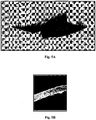
- the transparent conductive films of the present invention are generally characterized by an array of ring structures, which, in some embodiments of the invention, are spaced-apart material-free voids (or holes) in a continuum of a conductive material surface, and in others are intersecting conductive rings constructed of a conductive material on a non-conductive surface.
- the films of the invention are thus characterized by an array of conductive lines composed of conducting materials surrounding empty two dimensional material-voids, as further disclosed hereinbelow.
- a process for the manufacture of a conductive transparent film on a substrate comprising:
- the process comprises:
- the " material-free voids" are empty cells, openings, in the film of the first or conductive material, through which the substrate is exposed.
- the voids are separated by a conductive material which forms a continuous pattern.
- the conductive material is substantially a network of thin lines between the material-free voids.
- the voids are substantially free of the first or conductive material.
- the voids are further characterized hereinbelow.
- the conductive transparent film (the first material in the above aspect of the invention) is produced on a " substrate " which may be a flexible or rigid substrate, which may be substantially two-dimensional (a thin flat substrate) or a three-dimensional curved (non-flat) surface.
- the substrate can be of any smoothness.
- the substrate may be of a solid material such as glass, paper, a semiconductor inorganic or organic, a polymeric material or a ceramic surface.
- the surface material, being the substrate on which the film (of the first material or conductive material) is formed, may not necessarily be of the same material as the bulk of the object on the surface of which the film is produced.
- the substrate is an inorganic semiconductor material, including but not limited to, silicon, tin, compounds of boron, tellurium, geranium, gallium, gallium arsenide (GaAs), gallium phosphide (GaP), cadmium telluride (CdTe), gallium aluminum arsenide (GaAlAs), indium phosphide (InP), gallium arsenide phosphide (GaAsP), cadmium sulfide (CdS), copper indium gallium diselenide (CIGS), mercury cadmium telluride (HgCdTe), and copper indium sulfide or selenide.
- silicon tin
- the substrate may be of a polymeric material such as a polyamide, polyester, a polyacrylate, a polyolefin, a polyimide, a polycarbonate and polymethyl methacrylate.
- a polymeric material such as a polyamide, polyester, a polyacrylate, a polyolefin, a polyimide, a polycarbonate and polymethyl methacrylate.
- the substrate is coated on at least a region of its surface by a first material which is conductive or rendered conductive by any one method, thereby obtaining a conductive film or pattern on the at least a region of the substrate surface.
- the conductivity (or resistance) and transparency of the film is measured within the boundaries of the coated at least a region of the substrate.
- the at least a region of the surface may be the complete surface of the substrate or one or more regions of the substrate which may be connected to each other or in the vicinity of the other or spaced apart.
- the regions need not be of any predetermined size or shape.
- the regions may be in the form of a desired predetermined pattern.
- the first material e.g., conductive or precursor thereof, may be applied to the substrate by any means available so as to form a film of a desired thickness.
- the material may be applied by ink jetting by an ink-jet printer, by spraying by a sprayer or any other method such as air brush, by brushing the surface, by dipping the substrate into a liquid carrier comprising the, e.g., conductive material, by the doctor blade method, spin and roll-to-roll coating or by any other means as known in the art.
- the material droplets may be in the range of 1 picoliter to 10 microliter.
- the first material or the conductive material is typically selected from a metal, a transition metal, a semiconductor, an alloy, an intermetallic material, a conducting polymer, a carbon based material such as carbon black, carbon nanotubes (CNT), graphite, graphene, fullerenes, and carbon allotropes.
- the conductive material may be a combination of two or more different materials which are deposited on the substrate as a mixture to form, or step-wise. In some embodiments, the two or more different conductive materials are deposited on the substrate to form a plurality of ring structures, each ring structure being of a different conductive material as defined above.
- the two or more different conductive materials are deposited step-wise to form a conductive multilayer, each layer (film) being composed of a plurality of ring structures and being of a different material or material form.
- each layer (film) being composed of a plurality of ring structures and being of a different material or material form.
- two or more materials may be present in equal amounts or at any ratio, or where one of the materials is used as a dopant of the other.
- the conductive material is or comprises an element of Groups IIIB, IVB, VB, VIB, VIIB, VIIIB, IB, IIB, IIIA, IVA and VA of block d of the Periodic Table of the Elements.
- the conductive material is or comprises a transition metal selected from Groups IIIB, IVB, VB, VIB, VIIB, VIIIB, IB and IIB of block d the Periodic Table.
- the transition metal is a metal selected from Sc, Ti, V, Cr, Mn, Fe, Ni, Cu, Zn, Y, Zr, Nb, Tc, Ru, Mo, Rh, W, Au, Pt, Pd, Ag, Mn, Co, Cd, Hf, Ta, Re, Os, Ir and Hg.
- the conductive material is selected, in a non-limiting fashion, from indium(III) acetate, indium(III) chloride, indium(III) nitrate, indium(III) acetylacetonate, for the creation of CuInS 2 and Cu(InGa)S 2 ; iron(II) chloride, iron(III) chloride, iron(II) acetate, iron(III) acetylacetonate for the formation of CuFeS 2 ; gallium(III) acetylacetonate, gallium(II) chloride, gallium(III) chloride, gallium(III) nitrate for the formation of CuGaS 2 and Cu(InGa)S 2 ; aluminum(III) chloride, aluminum(III) stearate for the formation of CuAlS 2 ; silver nitrate, silver chloride for the formation of AgS; dimethlyzinc, diethylzinc, zinc chloride, tin(II)
- the conductive material is selected amongst semiconductor materials.
- the semiconductor material may be selected from elements of Group II-VI, Group III-V, Group IV-VI, Group III-VI, Group IV semiconductors and combinations thereof.
- the semiconductor material is a Group II-VI material being selected from CdSe, CdS, CdTe, ZnSe, ZnS, ZnTe, HgS, HgSe, HgTe, CdZnSe and any combination thereof.
- Group III-V material are selected from InAs, InP, InN, GaN, InSb, InAsP, InGaAs, GaAs, GaP, GaSb, AlP, AlN, AlAs, AlSb, CdSeTe, ZnCdSe and any combination thereof.
- the semiconductor material is selected from Group IV-VI, the material being selected from PbSe, PbTe, PbS, PbSnTe, Tl 2 SnTe 5 and any combination thereof.
- the conductive material is selected amongst metal alloys and intermetallics of the above metal and/or transition metals.
- Non-limiting examples of such alloys are WMo, MoRh, MoRh 3 , Ph 0.34 Ru 0.66 , Ph 0.4 Ru 0.6 , PdRh, PdRu, MoPd 2 , Pd 0.3 Mo 0.8 , MoPt, Mo 2 Pt, PtPd, Pt 0.4 Ru 0.6 , Pt 0.2 Ru 0.8 , PtRh, WPt, AuPd, AuPt, AuRh, AuRu, AuMo, and AuW.
- the conductive material is a carbon based material such as carbon black, carbon nanotubes (CNT), graphite, graphene, fullerenes, or other carbon allotropes.
- the conductive material may alternatively be a conductive polymer such as poly(3,4-dioctyloxythiophene) (PDOT), poly(3,4-ethylenedioxythiophene):poly (styrenesulfonate) (PDOT:PSS), polyaniline and polypyrrole.
- PDOT poly(3,4-dioctyloxythiophene)
- PDOT poly(3,4-ethylenedioxythiophene):poly (styrenesulfonate)
- PDOT polyaniline
- polypyrrole polypyrrole
- the conductive film is obtained by treating the substrate with a first material which is electrically non-conductive at the deposition step, but can be made conductive after further treatment (e.g., heating).
- the posttreatment for rendering the non-conductive material conductive include, in a non-limiting fashion, heating, chemical treatment, plasma, UV, laser, or microwave irradiation, flash lamp (Xenon) electroless plating, further coating and others.
- a non-conductive material such as a silver precursor, may be deposited on the substrate and rendered conductive, subsequent to hole printing by, e.g., heating.
- the conductive material is in the form of particles, e.g., nanoparticles.
- the conductive material is typically dispersed or dissolved in a liquid carrier prior to application for ease of accurate delivery.
- the liquid carrier may be selected from water and organic solvents.
- the liquid carrier may comprise at least one additional material for endowing specific functionality or enhancing the any one property of the film, such functionalities or property may be wetting, rheology, adhesion, doping, scratch resistance, contact and sheet resistance or preferential diffusion into an adjacent layer.
- additional material may include glass frits and inorganic salts.
- glass frits may be added to the conductive formulation prior to application to aid inter-diffusion and adhesion with a silicon-based semiconductor layer as known in silicon based photovoltaic cells.
- the conductive film is treated with at least one second material which is capable of displacing the conductive material in the film upon contact, at the so-called point of contact, clearing a void, hole or a cell in the conductive layer.
- the at least one second material differs from the first material of the conductive film by at least one chemical or physical parameter which permits the eventual displacement of material from the conductive film.
- Such parameter may be of the material itself or of the solution (solvent) in which it is dispersed, dissolved or otherwise carried; the parameter being selected from hydrophilicity, hydrophobicity, wetting behavior, surface tension and surface energy, spreading coefficient, evaporation rate, viscosity and other parameters.
- the at least one second material e.g., liquid, can be deposited on the film at various stages of evaporation of the wet film, as long as the displacement process is enabled.
- the first material is a hydrophobic solvent with conductive material in the form of nanoparticles and the at least one second material deposited as individual droplets on top of the film of the conductive material is carried in an aqueous medium. Due to the difference between the two materials, the aqueous material spreads over the wet film of nanoparticles, and due to surface energy effects come into contact with the substrate, thus forming material-free voids in the form of rings or holes, while pushing the nanoparticles to the rim of the material droplets. This eventually results, in this example, in narrow lines composed of closely packed nanoparticles and empty two dimensional voids.
- the dimensions of the material voids may be controlled by the size of the aqueous droplets, the competitive wetting of the droplets and the wet dispersion conductive film, the kinetics of the spreading, evaporation and particle-particle interactions.
- the conductive film is a solvent-based (nonaqueous) material containing metallic nanoparticles.
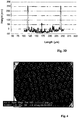
- the density of the voids (holes, cells) in the conductive layer should be such that the width between the voids of the remaining conductive material is less than 50 microns (between 1 and 50 microns) and in some cases at most 20 microns (between 1 and 20 microns).
- the final conductivity of the transparent film may also depend on several other parameters and the final coating may therefore, in certain embodiments, require additional processing to achieve high conductivity/transparency.
- Such processing may be heating, plasma, UV, laser, or microwave irradiation, flash lamp (Xenon) electroless plating, further coating and others.
- the height of the void rims is less than 10 microns and the average void diameter is less than 500 microns.
- the void diameter is between 10 and 300 microns, e.g., about 200 microns depending on the equipment used for deposition of the droplets.
- Small network cell size is preferred for low resistance losses in photovoltaic devices utilizing highly resistive materials (e.g. amorphous silicon or organic cells).
- highly resistive materials e.g. amorphous silicon or organic cells.
- the resistance associated with lateral motion of charge carriers from the middle of the void that is generally no larger than the resistance associated with vertical motion of the carriers within the semiconductor layer, i.e., the path length for moving carriers for a small network cell is no longer horizontally than vertically. Larger network void diameters could generate substantially greater ohmic losses and are thus generally not preferred.
- the film having the material-free void pattern has a sheet resistance (if composed of nanoparticles, as measured after sintering) of between 0.004 Ohm/square to 5 kOhm/square, in some cases less than 50 ohm/sq, less than 20 ohm/sq, less than or equal to 7 ohm/sq.
- the exhibited sheet resistance may be attributed to a close packing of the conductive material forming the conductive pattern, but may also be attributed to a post-jetting sintering process, as further disclosed below. Sheet resistance may be further reduced by subsequent electroplating of the deposited pattern.
- the transparent conductive films of the invention are particularly useful in devices that require transmission of visible, NIR, IR, and/or UV regions of the electromagnetic spectrum.
- the light transparency of the layers is of at least 30%, in some embodiments at least 50%, in other embodiments at least 70% and in further embodiments of about 95% and more light transparency.
- transmission is measured in the wavelength range of 400nm to 700nm.
- the films manufactured in accordance with the present invention are characterized by a transparency of 95% and a sheet resistance of between 0.004 Ohm/square to 5 kOhm/square.
- the resistivity of the film is 4 ⁇ 0.5 Ohm/square over 0.5 cm 2 .
- the invention further provides a substrate, as defined herein, coated with a conductive transparent film of a material having a plurality of spaced-apart ring-voids, the rim of each of said plurality of spaced-apart voids is less than 10 microns and the average void-diameter is less than 500 microns.
- the average void diameter is between 10 and 300 microns. In other embodiments, the average void diameter is between about 200 and 300 microns.
- the width of the conductive material between the voids is smaller than 60 micron
- the conductive transparent film is characterized by a light transparency of 95% and a sheet resistance of between 0.004 Ohm/square to 5 kOhm/square.
- the resistivity of the conductive transparent film is 4 ⁇ 0.5 Ohm/square over 0.5 cm 2 .
- the invention also provides a substrate, as defined herein, coated with a conductive transparent film of a material having a plurality of spaced-apart voids, the rim of each of said plurality of spaced-apart voids is less than 10 microns and the average hole-diameter is less than 500 microns, wherein the film has an overall transparency of 95% and a sheet resistance of between 0.004 Ohm/square to 5 kOhm/square.
- the invention also provide a conductive transparent film of a material, said film having a plurality of spaced-apart material voids, the rim of each of said plurality of spaced-apart voids is less than 10 microns and the average hole-diameter is less than 500 microns, wherein the film has an overall transparency of 95% and a sheet resistance of between 0.004 Ohm/square to 5 kOhm/square.
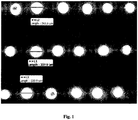
- FIG. 1 A conductive transparent film according to the above aspect of the invention is shown in Fig. 1 .
- the film was prepared by inkjet printing of drops of a single aqueous solution (the second material) on a wet film of solvent-based silver dispersion (the first material).
- the application of the aqueous droplets onto the silver film caused a replacement of the silver solvent dispersion/substrate interface with the aqueous solution/substrate interface, resulting in empty cells, material-free voids.
- the silver particles, which were displaced to the rim of the droplet formed a darker area, typical for more condensed packing of the particles.
- a process for the manufacture of a conductive transparent pattern on a substrate comprising treating a substrate with a plurality of droplets of a conductive material, permitting said droplets to form an array of intersecting ring-structures on the substrate, wherein the conductive material is selected from (1) a combination of two or more metals or precursors thereof, (2) a semiconductor material, (3) a carbon based material such as carbon black, carbon nanotubes (CNT), and other carbon allotropes, (4) quantum dots, and (5) any mixture of the aforementioned, to thereby obtain a conductive transparent pattern on the substrate.
- the conductive material is selected from (1) a combination of two or more metals or precursors thereof, (2) a semiconductor material, (3) a carbon based material such as carbon black, carbon nanotubes (CNT), and other carbon allotropes, (4) quantum dots, and (5) any mixture of the aforementioned, to thereby obtain a conductive transparent pattern on the substrate.
- the conductive transparent coating is obtained by self-assembly of a conductive material.
- the self-assembly permits the formation of arrays of interconnected micrometric rings.
- the rim of each ring has a width of between 1-10 microns (in some embodiments, 1-5 microns, in other embodiments, 2-9 microns, in further embodiments, 3-9 microns, or 2-6 microns) and is composed of closely packed nanoparticles. Such an arrangement results in high electrical conductivity.
- the center of each ring is actually a hole, having a diameter of between about 100 and 200 microns. Due to the small dimensions, the whole array of the interconnected rings is optically transparent and maintains its high conductivity.
- the conductive arrays may be obtained by inkjet printing of picoliter droplets of a dispersion of at least one conductive material, as defined hereinabove, e.g., silver, onto a substrate, as defined hereinabove. After printing, each printed dot is self-assembled into a ring, by the well known "coffee ring effect". This effect may be utilized, in accordance with the invention, for obtaining a functional property, namely transparency and conductivity, by forming tow-dimensional arrays of interconnected conductive rings. The fabrication of the arrays is spontaneous, with a low cost process of inkjet printing. The resulting conductivity and transparency of these are comparable to that of ITO.
- a functional property namely transparency and conductivity
- two or more such materials may be used for improving one or more properties of the array.
- dispersions containing a mixture of two or more conductive nanoparticles segregation ( Fig. 2 ) can be obtained.
- the two nanoparticle-populations may differ by size, protective molecule, dispersant or coating.
- the invention thus provides a substrate, as defined hereinabove, coated with a conductive transparent film, the film having a pattern of intersecting ring structures of a conductive material selected from (1) a combination of two or more metals or precursors thereof, (2) a semiconductor material, (3) carbon based materials such as carbon black, carbon nanotubes (CNT), and other carbon allotropes, (4) quantum dots, and (5) any mixture of the aforementioned, the rim of each ring structure has a width of between about 1-5 microns, the diameter of each ring structure is between about 100 and 200 micrometer.
- the present invention provides in a further of its aspects, a device implementing at least one conductive transparent film according to the present invention.
- the conductive transparent film having a plurality of spaced-apart ring-voids, the rim of each of said plurality of spaced-apart voids is less than 10 microns and the average void-diameter is less than 500 microns.
- the average void diameter in the film is between 10 and 300 microns. In other embodiments, the average void diameter in the film is between about 200 and 300 microns.
- the width of the conductive material between the voids is smaller than 60 micron
- the film implemented in the device of the invention is further characterized by having at least one attribute selected from:
- the conductive transparent film implemented in the device is characterized by a light transparency of 95% and a sheet resistance of between 0.004 Ohm/square to 5 kOhm/square.
- the resistivity of the conductive transparent film is 4 ⁇ 0.5 Ohm/square over 0.5 cm 2 .
- the invention also provides a device implementing a conductive transparent film having a plurality of spaced-apart voids, the rim of each of said plurality of spaced-apart voids is less than 10 microns and the average hole-diameter is less than 500 microns, wherein the film has an overall transparency of 95% and a sheet resistance of between 0.004 Ohm/square to 5 kOhm/square.
- the invention also provides a device implementing a conductive transparent film having a pattern of intersecting ring structures of at least one conductive material.
- the conductive material is as defined hereinabove.
- the conductive material is non-metallic.
- the conductive material is selected from (1) a combination of two or more metals or precursors thereof, (2) a semiconductor material, (3) carbon based materials such as carbon black, carbon nanotubes (CNT), and other carbon allotropes, (4) quantum dots, and (5) any mixture of the aforementioned.
- the conductive transparent film implemented in the device has a width of between about 1-5 microns, the diameter of each ring structure is between about 100 and 200 micrometer.
- the conductive transparent film is constructed of at least two intersecting ring structures or at least two layered films of intersecting ring structures, wherein the ring structures are composed of different conductive materials, as defined hereinabove.
- the at least two intersecting ring structures are composed of two or more different conductive materials.
- the at least two layers of intersecting ring structures are constructed of layered films of ring structures, each film being of a different conductive material or composed of ring structures of different conductive materials.
- the layer implemented in the device of the invention is manufactured according to the process comprising:
- the layer in the device is manufactured according to the process comprising:
- the invention also provides a device implementing a conductive transparent multilayer, said multilayer being composed of a plurality of films, each film of said multilayer being composed of a plurality of ring structures.
- each layer may be of a different material or material form or composed of a plurality of ring structures of different materials or material forms.
- the substrate on which the film is provided may be an integral part of the device or may be a substrate which following its treatment as recited is implemented in the device.
- the device may be an electronic device or an optoelectronic device.
- an additional layer over the transparent conductive film may be formed by plating.
- a protective layer over the metal e.g., silver, may be useful.
- optoelectronics is the study and application of electronic devices that source, detect and control light; such devices may be electrical-to-optical and/or optical-to-electrical transducers.
- the conductive transparent films produced in accordance with the invention can be employed as conductive transparent electrodes, replacing ITO as the material of choice.
- the films manufactured according to the invention exhibit higher transparency and thus lead to higher efficiency of the optoelectronic device.
- the transparent conductive films of the invention may be integrated in devices, that requires transmittance of visible, UV, IR, and/or NIR regions of the electromagnetic spectrum, including for example, photoconductors, photodiodes; solar cells; light emitting diodes (LEDs), including organic light emitting diodes and lasers; light sensors, as well as specialized transistors, including organic transistors, inorganic transistors, or hybrid transistors.
- Other applications for utilization of such coatings are related to the following categories: printed electronics, touch screens, display backplanes and large or small area flexible applications. Flexible applications further include large area arrays, flexible displays, and e-paper (electronic books, journals, newspapers).
- the conductive transparent films may further find utility in monitoring or detection devices for healthcare, security or safety-related uses, including low-cost or disposable sensors or optical devices, as well as in smart packaging such as for incorporation of tags or RFID components into the packaging.
- the technology can be employed in building applications such as smart windows, or in specialty coatings and paints which function as part of a semiconductor device.
- the optoelectronic device is photovoltaic solar cells.
- the transparent conductive film which is produced according to the processes of the present invention may be integrated as follows:
- the transparent electrode composed of conductive rings or conductive patterns connecting the holes and produced by the present invention may also have a lower resistivity than ITO while maintaining light transmittance. Lower resistivity can lead to lower power losses, for example, in conversion of optical power to electrical power in solar cells. Further, the geometry of the ring pattern of the transparent electrode is advantageous over the geometry of a conventional silver grid due to higher transparency.
- the line width of screen-printed grids is typically quite large (100 microns) in comparison to the line width of the rings forming the array of the present transparent electrodes ( ⁇ 10 microns). Reduced line widths allow greater transparency.
- the fabrication methods for transparent electrodes used in the present invention can also be used to form electromagnetic shielding (EMS).
- EMS electromagnetic shielding
- the transparent conductive patterns provided in accordance with the processes of the present invention are better alternatives to the widely used transparent conductive oxides, such as ITO, and can be utilized in optoelectronic devices such as solar cells.
- the new transparent conductive coatings are achieved by forming a 2-D array of interconnected rings or array of holes, while the rim of the ring and the spaces in between the holes is composed of a conducting material such as metallic nanoparticles.
- the rim of the individual rings has a width of below 50 microns and a height below 300 nm, which surrounds a "hole” with a controllable diameter for example diameter of about 150 micron, and therefore the whole array of the interconnected rings is invisible to the naked eye.
- the rims of the rings are composed of self-assembled, closely packed nanoparticles, which make the individual rings and the resulting array electrically conductive.
- arrays of holes is based on controlled wetting which induces, in case of metallic nanoparticles, their self-assembly into predetermined narrow patterns around two-dimensional empty cells.
- the conducting material concentrates at the rims (in case of ring formation) or in between empty spaces (in case of holes formation).
- transparent conductive coatings which are obtained by printing metallic (or semiconductor) particles was demonstrated while using it as the transparent electrode on a plastic electroluminescent device, demonstrating the applicability of this concept in plastics electronics.
- Such transparent conductive coatings can be used in a wide range of applications such as displays (LCD, Plasma, touch screens, e-paper), lighting devices (electroluminescence, OLED) and solar cells.
- a glass slide was coated by a solvent based silver ink (solvent with dispersed silver nanoparticles) by draw down. Before the total evaporation of the solvent, an aqueous solution was printed on top of the coat by ink-jet printing (MicroFab, 60um wide nozzle). The solution contained 0.05% of a wetting agent (BYK 348) The printed droplets led to the de-wetting of the silver ink at the printing zone, i.e., to the formation of holes (an area which does not contain the conducting material). The area with holes can be further treated if required to obtain conductivity. For example, if the conducting material is silver nanoparticles, the substrate can be sintered at elevated temperature, or by other chemical means.
- Single rings with a diameter of ⁇ 150 micrometer were obtained by ink-jetting a silver ink (prepared as described elsewhere [ 14 ]) on polyethylene terphthalate (PET) substrate with the single nozzle print-head.
- PET polyethylene terphthalate
- the aqueous ink contained 0.5 wt% dispersed silver nanoparticles, with a diameter of 5 to 20 nm, stabilized by polyacrylic acid.
- the surface tension of the ink was adjusted to 30 mN/m by the use of Byk®348 (BykCheime).
- the pH was set to 10 using amino methyl propanol.
- the printing of the dispersion was performed by Microfab®JetDriveTM III printer with a 60 micrometer wide single nozzle.
- the applied waveform for all the printing experiments was: voltage 110 V, rise time 3 microsec, echotime 15 microsec, dwell time 30 microsec fall time 5 microsec.
- the voltage increased (from the minimal voltage of 20 V), the droplet size increased as well, thus enlarging the ring diameter. Further increase above 110V, was not tested due to device limitation.
- the dwell time was also increased in steps of 5 microsec up to a value of 40 microsec (in each change the echo-time was double the value of the dwell time), which also caused the droplet and ring diameter to increase. Changing the dwell time and the voltage did not affect the edge profile, as it remained in a parabolic shape.
- the movement of the substrate was performed by a DMC-21x3XY table (Galil Motion Control, Inc.).
- the substrate temperature was set to 30°C with a Peltier heater/cooler, and humidity within the printing chamber was 30-40% RH.
- each ring should be conductive. Therefore, at the first stage, resistivity measurements of individual rings were performed by connecting the ring to microelectrodes obtained by vapor deposition of Au/Cr bi-layer through a suitable mask.
- FIG. 5A The topographic 3-D ( FIG. 5A ) image shows a continuous line having maximal height of 400 nm and width of about 7 ⁇ m.
- the corresponding 2-D current map ( Fig. 5C ) and image ( Fig.5B ) show that the line is indeed conductive. It should be emphasized that even though a small area of the ring is scanned, the fact that this area of the ring is conductive proves electrical continuity over a much larger range, at least as far as the distance to the Au/Cr counter electrode.
- Chains composed of overlapping printed rings printed as described in Example 2 were obtained by printing a first forward line of rings with pre-determined spaces between the rings, followed by printing a backward, second line of rings, with a proper distance adjustment between the two lines. Optimization of the chain formation process was achieved by adjusting the jetting frequency (35 Hz) and the substrate movement (10000 micrometer/s). Part of such a chain is shown in Figs. 6A-C.
- Two-dimensional (2-D) arrays of such rings were formed by repeating the chain formation procedure for a large number of lines, while keeping a constant distance between the lines.
- 2-D arrays composed of connected chains could be obtained.
- the array is actually composed mainly of holes (the inner part of each ring), ⁇ 150 micrometer in diameter, which are connected by narrow lines, about 5 micrometer in width, located around each hole.
- the sheet resistance of such a 2-D array (sample area of 0.5 cm 2 ) was very low, 4 ⁇ 0.5 Ohm/square. It should be noted that qualitative bending experiments show that these values remained constant even after bending the substrate at angles below about 20°, showing that the arrays may be suitable for applications in which flexibility is required.
- the typical sheet resistance of ITO thin films that have more than 80% transparency is much greater, in the range of 20-100 Ohm/square.
- the 5 micrometer lines are almost invisible to the naked eye, thus the 2-D pattern is almost transparent.
- the transmittance measured by a spectrophotometer at 400-800 nm was as great as 95( ⁇ 3) % T.
- these conductive arrays were evaluated as the transparent electrode in an electroluminescent device.
- the device was fabricated on top of the transparent ring array by depositing layers of ZnS, and BaTiO 3 by conventional screen printing, followed by deposition of a second silver electrode.
- the printed ring array is indeed conductive and transparent.
- the decay length for emission was estimated to be about 20 ⁇ m).
Claims (17)
- Verfahren zur Herstellung eines leitenden transparenten Films auf einem Substrat, wobei das Verfahren Folgendes umfasst:- Beschichten eines Substrats durch ein erstes Material, um einen nassen Film aus dem ersten Material auf zumindest einem Bereich einer Oberfläche des Substrats zu bilden, wobei das erste Material leitend ist oder wobei der Film behandelt ist, um das erste Material leitend zu machen; und- Behandeln des Films mit zumindest einem zweiten Material, das dazu in der Lage ist, das erste Material in dem Film an dem Kontaktpunkt zu verschieben; was zu Verschiebung des Filmmaterials von dem Kontaktpunkt und Exposition des Substrats führt, um eine Anordnung an beabstandeten Ringhohlräumen in dem Film bereitzustellen.
- Verfahren nach Anspruch 1, wobei das Substrat aus einem Material ist, das aus Glas, Papier, einem anorganischen oder organischen Halbleitermaterial, einem Polymermaterial und einem Keramikmaterial ausgewählt ist.
- Verfahren nach Anspruch 2, wobei das Substrat ein anorganisches Halbleitermaterial ist, das aus Silizium, Zinn, Verbindungen aus Bor, Tellur, Geranium, Gallium, Galliumarsenid (GaAs), Galliumphosphid (GaP), Cadmiumtellurid (CdTe), Galliumaluminiumarsenid (GaAlAs), Indiumphosphid (InP), Galliumarsenidphosphid (GaAsP), Cadmiumsulfid (CdS), Kupferindiumgalliumdiselenid (CIGS), Quecksilbercadmiumtellurid (HgCdTe), Kupferindiumsulfid und Kupferindiumselenid ausgewählt ist.
- Verfahren nach Anspruch 2, wobei das Substrat aus einem Polymermaterial ist, das aus einem Polyamid, Polyester, einem Polyacrylat, einem Polyolefin, einem Polyimid, einem Polycarbonat und Polymethylmethacrylat ausgewählt ist.
- Verfahren nach Anspruch 1, wobei das erste Material aus einem Metall, einem Übergangsmetall, einem Halbleiter, einer Legierung, einem intermetallischen Material, einem leitenden Material und einem kohlenstoffbasierten Material ausgewählt ist.
- Verfahren nach Anspruch 5, wobei das erste Material ein leitendes Polymer ist.
- Verfahren nach Anspruch 6, wobei das leitende Polymer aus poly(3,4-Dioctyloxythiophen) (PDOT), poly(3,4-Ethylendioxythiopen):poly(Styrolsulfonat) (PDOT:PSS), Polyanilin und Polypyrrol ausgewählt ist.
- Verfahren nach Anspruch 5, wobei das erste Material eine Kombination aus zwei oder mehreren verschiedenen leitenden Materialien ist, die auf dem Substrat abgelagert sind, um eine Vielzahl von Ringstrukturen zu bilden, die jeweils aus einem anderen leitenden Material sind, oder stufenweise abgelagert sind, um eine leitende Multischicht zu bilden, wobei jede Schicht aus einer Vielzahl von Ringstrukturen besteht und aus einem/einer anderen Material oder Materialform ist.
- Substrat, das mit einem leitenden transparenten Film eines Materials beschichtet ist, das eine Vielzahl von beabstandeten materialfreien Hohlräumen aufweist, wobei der Rand von jedem aus der Vielzahl von beabstandeten Hohlräumen weniger als 10 Mikrometer beträgt und der durchschnittliche Hohlraumdurchmesser weniger als 500 Mikrometer beträgt.
- Substrat nach Anspruch 9, dadurch gekennzeichnet, dass es zumindest eines des Folgenden aufweist:a. eine Hohlraumbeabstandung von weniger als 50 Mikrometern;b. einen Schichtwiderstand zwischen 0,004 Ohm/Quadrat und 5 kOhm/Quadrat; undc. eine Lichttransparenz von zumindest 30 %.
- Substrat, das mit einem leitenden transparenten Film eines Materials beschichtet ist, das eine Vielzahl von beabstandeten materialfreien Hohlräumen aufweist, wobei der Abstand zwischen jedem aus der Vielzahl von beabstandeten Hohlräumen weniger als 10 Mikrometer beträgt und der durchschnittliche Hohlraumdurchmesser weniger als 500 Mikrometer beträgt, wobei der Film eine Gesamttransparent von 95 % und einen Schichtwiderstand zwischen 0,004 Ohm/Quadrat und 5 kOhm/Quadrat aufweist.
- Substrat nach einem der Ansprüche 9-11, hergestellt gemäß dem Verfahren nach einem der Ansprüche 1 bis 8.
- Verfahren zur Herstellung eines leitenden transparenten Musters auf einem Substrat, wobei das Verfahren das Behandeln eines Substrats mit einer Vielzahl von Tröpfchen eines leitenden Materials umfasst, wodurch erlaubt wird, dass die Tröpfchen eine Anordnung an sich schneidenden Ringstrukturen auf dem Substrat bilden, wobei das leitende Material aus (1) einer Kombination aus einem oder mehreren Metallen oder Vorläufern davon, (2) einem Halbleitermaterial, (3) einem kohlenstoffbasierten Material, (4) Quantenpunkten und (5) einem beliebigen Gemisch aus dem Vorstehenden ausgewählt ist, um dadurch ein leitendes transparentes Muster auf dem Substrat zu erhalten, wobei der Rand jedes Rings eine Breite zwischen 1 und 10 Mikrometern aufweist.
- Substrat, das mit einem leitenden transparenten Film beschichtet ist, wobei der Film ein Muster aus sich schneidenden Ringstrukturen eines leitenden Material aufweist, das aus (1) einer Kombination aus einem oder mehreren Metallen oder Vorläufern davon, (2) einem Halbleitermaterial, (3) einem kohlenstoffbasierten Material, (4) Quantenpunkten und (5) einem beliebigen Gemisch aus dem Vorstehenden ausgewählt ist, wobei der Rand jeder Ringstruktur eine Breite zwischen ungefähr 1 und 5 Mikrometern aufweist, wobei der Durchmesser jeder Ringstruktur ungefähr 100 bis 200 Mikrometer beträgt.
- Substrat nach Anspruch 14, wobei der Film durch zumindest eines des Folgenden gekennzeichnet ist:a. einen Schichtwiderstand zwischen 0,004 Ohm/Quadrat und 5 kOhm/Quadrat; undb. eine Lichttransparenz von zumindest 30 %.
- Bauelement, das einen leitenden transparenten Film umsetzt, wobei der Film ein Muster aus sich schneidenden Ringstrukturen aus zumindest einem leitenden Material aufweist.
- Bauelement, das eine leitende transparente Multischicht umsetzt, wobei die Multischicht aus einer Vielzahl von Filmen besteht, wobei jeder Film der Multischicht aus einer Vielzahl von sich schneidenden Ringstrukturen aus zumindest einem leitenden Material besteht und aus einem/einer anderen Material oder Materialform ist.
Applications Claiming Priority (2)
| Application Number | Priority Date | Filing Date | Title |
|---|---|---|---|
| US25713909P | 2009-11-02 | 2009-11-02 | |
| PCT/IL2010/000909 WO2011051952A2 (en) | 2009-11-02 | 2010-11-02 | Transparent conductive coatings for optoelectronic and electronic devices |
Publications (2)
| Publication Number | Publication Date |
|---|---|
| EP2496661A2 EP2496661A2 (de) | 2012-09-12 |
| EP2496661B1 true EP2496661B1 (de) | 2018-07-11 |
Family
ID=43827776
Family Applications (1)
| Application Number | Title | Priority Date | Filing Date |
|---|---|---|---|
| EP10790862.6A Not-in-force EP2496661B1 (de) | 2009-11-02 | 2010-11-02 | Transparente leitende beschichtungen für optoelelektronische und elektronische bauelemente |
Country Status (6)
| Country | Link |
|---|---|
| US (2) | US9107275B2 (de) |
| EP (1) | EP2496661B1 (de) |
| JP (2) | JP2013531861A (de) |
| KR (1) | KR20120104565A (de) |
| CN (1) | CN102714903B (de) |
| WO (1) | WO2011051952A2 (de) |
Families Citing this family (34)
| Publication number | Priority date | Publication date | Assignee | Title |
|---|---|---|---|---|
| PT2456918T (pt) | 2009-07-22 | 2016-12-07 | Hampidjan Hf | Corda helicoidal com menor força de arrastamento para redes de arrasto pelágico e métodos |
| US8933906B2 (en) | 2011-02-02 | 2015-01-13 | 3M Innovative Properties Company | Patterned substrates with non-linear conductor traces |
| KR101846434B1 (ko) | 2011-06-10 | 2018-04-09 | 삼성디스플레이 주식회사 | 유기 발광 표시 장치 |
| US20130025662A1 (en) * | 2011-07-25 | 2013-01-31 | International Business Machines Corporation | Water Soluble Dopant for Carbon Films |
| CN102338941B (zh) * | 2011-09-06 | 2013-07-24 | 天津大学 | 碲化镉量子点接枝石墨烯-碳纳米管复合薄膜光开关材料及制备 |
| EP4052648A1 (de) * | 2011-11-17 | 2022-09-07 | Nippon Telegraph And Telephone Corporation | Leitfähige polymerfasern, verfahren und vorrichtung zur herstellung leitfähiger polymerfasern, biologische elektrode, vorrichtung zur messung biologischer signale, implantierbare elektrode und vorrichtung zum messen biologischer signale |
| DE102012201688A1 (de) * | 2012-02-06 | 2013-08-08 | Robert Bosch Gmbh | Solarzelle und Verfahren zu deren Herstellung |
| CN102594212A (zh) * | 2012-02-20 | 2012-07-18 | 北京航空航天大学 | 一种积木球壳火炬太阳能发电装置 |
| WO2014099080A2 (en) | 2012-09-26 | 2014-06-26 | University Of Florida Research Foundation, Inc. | Transparent quantum dot light-emitting diodes with dielectric/metal/dielectric electrode |
| US9786865B2 (en) * | 2013-04-01 | 2017-10-10 | Pioneer Corporation | Optical device |
| JP6266598B2 (ja) * | 2013-04-01 | 2018-01-24 | パイオニア株式会社 | 光学装置 |
| FI20135510L (fi) | 2013-05-14 | 2014-11-15 | Canatu Oy | Taipuisa valoa emittoiva kalvo |
| GB201310854D0 (en) | 2013-06-18 | 2013-07-31 | Isis Innovation | Photoactive layer production process |
| JP6536401B2 (ja) * | 2013-07-10 | 2019-07-03 | コニカミノルタ株式会社 | 塗膜形成方法、透明導電膜付き基材、デバイス及び電子機器 |
| SG11201601614YA (en) * | 2013-09-10 | 2016-04-28 | Univ Nanyang Tech | Electrochromic device |
| WO2015083160A2 (en) * | 2013-12-02 | 2015-06-11 | Clearjet Ltd | Process for controlling wettability features |
| US10465295B2 (en) | 2014-05-20 | 2019-11-05 | Alpha Assembly Solutions Inc. | Jettable inks for solar cell and semiconductor fabrication |
| JP6540698B2 (ja) | 2014-06-25 | 2019-07-10 | コニカミノルタ株式会社 | パターン形成方法、透明導電膜付き基材、デバイス及び電子機器 |
| CN111525018B (zh) * | 2014-08-06 | 2023-10-24 | Ns材料株式会社 | 树脂成型品、波长变换部件、以及照明部件 |
| CN113930707B (zh) | 2014-10-21 | 2024-04-16 | 奥雷尔科技有限公司 | 一种在基底上形成图案化金属膜的方法和系统 |
| KR102290310B1 (ko) * | 2014-11-14 | 2021-08-13 | 삼성전자주식회사 | 전도성 박막 |
| KR102266615B1 (ko) | 2014-11-17 | 2021-06-21 | 삼성전자주식회사 | 전계 효과 트랜지스터를 포함하는 반도체 소자 및 그 제조 방법 |
| GB201500748D0 (en) * | 2015-01-16 | 2015-03-04 | Cambridge Display Tech Ltd | Method of forming a light-emitting device |
| WO2016140284A1 (ja) | 2015-03-02 | 2016-09-09 | コニカミノルタ株式会社 | パターン形成方法、透明導電膜付き基材、デバイス及び電子機器 |
| WO2016143715A1 (ja) * | 2015-03-06 | 2016-09-15 | コニカミノルタ株式会社 | 透明導電体及び透明導電体の製造方法 |
| JP6413978B2 (ja) | 2015-08-21 | 2018-10-31 | コニカミノルタ株式会社 | 機能性細線パターン前駆体の形成方法、機能性細線パターンの形成方法、透明導電膜の形成方法、デバイスの製造方法及び電子機器の製造方法、並びに、機能性細線パターン、透明導電膜付き基材、デバイス及び電子機器 |
| US11001687B2 (en) | 2016-08-31 | 2021-05-11 | Konica Minolta, Inc. | Substrate with functional fine line and method for forming functional fine line |
| US10126656B2 (en) | 2016-09-08 | 2018-11-13 | Goodrich Corporation | Apparatus and methods of electrically conductive optical semiconductor coating |
| CN108659622B (zh) * | 2017-03-28 | 2021-05-04 | 京东方科技集团股份有限公司 | 导电油墨、显示基板及其制造方法和显示装置 |
| CN107556510B (zh) * | 2017-08-29 | 2020-06-05 | 浙江理工大学 | 一种柔性传感器电极的制备方法 |
| KR101947164B1 (ko) * | 2018-06-05 | 2019-02-13 | 삼성디스플레이 주식회사 | 유기 발광 표시 장치 및 그 제조 방법 |
| CN109307897B (zh) * | 2018-11-23 | 2021-04-27 | 淮阴工学院 | 一种可绕折的光扩散膜的制备方法 |
| CN109633950A (zh) * | 2019-02-20 | 2019-04-16 | 福州大学 | 一种用于集成成像2d/3d可切换显示的液晶透镜及其制备方法 |
| US11862746B2 (en) * | 2019-04-23 | 2024-01-02 | Syracuse University | Ultrawide-angle light collecting modules formed by direct light-writing of nanoparticle-based metallo-dielectric optical waveguides |
Family Cites Families (9)
| Publication number | Priority date | Publication date | Assignee | Title |
|---|---|---|---|---|
| US6197418B1 (en) * | 1998-12-21 | 2001-03-06 | Agfa-Gevaert, N.V. | Electroconductive glass laminate |
| JP4232480B2 (ja) | 2002-03-25 | 2009-03-04 | 住友金属鉱山株式会社 | 貴金属コート銀微粒子分散液の製造方法と透明導電層形成用塗布液および透明導電性基材と表示装置 |
| US7601406B2 (en) | 2002-06-13 | 2009-10-13 | Cima Nanotech Israel Ltd. | Nano-powder-based coating and ink compositions |
| US20070003743A1 (en) * | 2004-08-27 | 2007-01-04 | Masaaki Asano | Color filter substrate for organic EL element |
| JP2008527169A (ja) * | 2005-01-10 | 2008-07-24 | イシウム リサーチ デベロップメント カンパニー オブ ザ ヘブリュー ユニバーシティー オブ イエルサレム | 金属ナノ粒子の水系分散物 |
| US8330348B2 (en) | 2005-10-31 | 2012-12-11 | Osram Opto Semiconductors Gmbh | Structured luminescence conversion layer |
| JP2008130449A (ja) * | 2006-11-22 | 2008-06-05 | Alps Electric Co Ltd | 発光装置およびその製造方法 |
| TWI480653B (zh) | 2007-04-20 | 2015-04-11 | Cambrios Technologies Corp | 高對比透明導體及形成其之方法 |
| JP2009224078A (ja) * | 2008-03-14 | 2009-10-01 | Kyoto Univ | 透明導電膜及びその製造方法 |
-
2010
- 2010-11-02 CN CN201080060244.9A patent/CN102714903B/zh not_active Expired - Fee Related
- 2010-11-02 EP EP10790862.6A patent/EP2496661B1/de not_active Not-in-force
- 2010-11-02 KR KR20127014346A patent/KR20120104565A/ko not_active Application Discontinuation
- 2010-11-02 US US13/503,772 patent/US9107275B2/en not_active Expired - Fee Related
- 2010-11-02 JP JP2012536014A patent/JP2013531861A/ja active Pending
- 2010-11-02 WO PCT/IL2010/000909 patent/WO2011051952A2/en active Application Filing
-
2015
- 2015-01-30 JP JP2015016775A patent/JP2015146310A/ja active Pending
- 2015-07-06 US US14/792,092 patent/US9807848B2/en active Active
Non-Patent Citations (1)
| Title |
|---|
| None * |
Also Published As
| Publication number | Publication date |
|---|---|
| KR20120104565A (ko) | 2012-09-21 |
| JP2013531861A (ja) | 2013-08-08 |
| US20120204950A1 (en) | 2012-08-16 |
| US20150357511A1 (en) | 2015-12-10 |
| WO2011051952A2 (en) | 2011-05-05 |
| US9107275B2 (en) | 2015-08-11 |
| EP2496661A2 (de) | 2012-09-12 |
| CN102714903B (zh) | 2016-08-10 |
| WO2011051952A3 (en) | 2011-06-23 |
| JP2015146310A (ja) | 2015-08-13 |
| CN102714903A (zh) | 2012-10-03 |
| US9807848B2 (en) | 2017-10-31 |
Similar Documents
| Publication | Publication Date | Title |
|---|---|---|
| US9807848B2 (en) | Transparent conductive coatings for optoelectronic and electronic devices | |
| KR101234881B1 (ko) | 나노입자로 형성된 투명한 전극을 갖는 광전지 소자 | |
| Yang et al. | Designed assembly and integration of colloidal nanocrystals for device applications | |
| US20070001581A1 (en) | Nanostructure based light emitting devices and associated methods | |
| US20100003781A1 (en) | Roll-to-roll non-vacuum deposition of transparent conductive electrodes | |
| WO2012168941A1 (en) | Flexible transparent conductive coatings by direct room temperature evaporative lithography | |
| JP2012507872A (ja) | ハイブリッド透明導電性電極 | |
| WO2015083160A2 (en) | Process for controlling wettability features | |
| US20120292725A1 (en) | Deposition and post-processing techniques for transparent conductive films | |
| EP3323149A1 (de) | Verformbare optoelektronische vorrichtungen für papier-origami | |
| Pozov et al. | Up-scalable ITO-free organic light emitting diodes based on embedded inkjet-printed copper grids | |
| Xiao et al. | Emission spectroscopy investigation of the enhancement of carrier collection efficiency in AgBiS2-nanocrystal/ZnO-nanowire heterojunction solar cells | |
| CN109215687A (zh) | 用于光信息存储的柔性透明存储器及制备方法 | |
| US10290754B2 (en) | Light harvesting antenna complexes | |
| Mohammad et al. | Effect of substrates on structural, morphological, optical and electrical characteristics on poly (9, 9-di-n-octylfluorenyl-2, 7-diyl)(PFO) thin films | |
| YousefiAmin | Printed Thin Film Photodetectors | |
| Basavaraj et al. | Solution processing of active semiconducting polymers and conducting polymer anodes for fabricating photodetectors |
Legal Events
| Date | Code | Title | Description |
|---|---|---|---|
| PUAI | Public reference made under article 153(3) epc to a published international application that has entered the european phase |
Free format text: ORIGINAL CODE: 0009012 |
|
| 17P | Request for examination filed |
Effective date: 20120604 |
|
| AK | Designated contracting states |
Kind code of ref document: A2 Designated state(s): AL AT BE BG CH CY CZ DE DK EE ES FI FR GB GR HR HU IE IS IT LI LT LU LV MC MK MT NL NO PL PT RO RS SE SI SK SM TR |
|
| DAX | Request for extension of the european patent (deleted) | ||
| STAA | Information on the status of an ep patent application or granted ep patent |
Free format text: STATUS: EXAMINATION IS IN PROGRESS |
|
| 17Q | First examination report despatched |
Effective date: 20170307 |
|
| REG | Reference to a national code |
Ref country code: DE Ref legal event code: R079 Ref document number: 602010051878 Country of ref document: DE Free format text: PREVIOUS MAIN CLASS: C09K0011020000 Ipc: H01B0001020000 |
|
| GRAP | Despatch of communication of intention to grant a patent |
Free format text: ORIGINAL CODE: EPIDOSNIGR1 |
|
| STAA | Information on the status of an ep patent application or granted ep patent |
Free format text: STATUS: GRANT OF PATENT IS INTENDED |
|
| RIC1 | Information provided on ipc code assigned before grant |
Ipc: C23C 4/18 20060101ALI20180110BHEP Ipc: H01L 31/18 20060101ALI20180110BHEP Ipc: H01B 1/10 20060101ALI20180110BHEP Ipc: H05K 1/02 20060101ALI20180110BHEP Ipc: H05K 3/12 20060101ALI20180110BHEP Ipc: H05K 1/03 20060101ALI20180110BHEP Ipc: C23C 26/00 20060101ALI20180110BHEP Ipc: H05K 1/09 20060101ALI20180110BHEP Ipc: H01B 1/02 20060101AFI20180110BHEP |
|
| INTG | Intention to grant announced |
Effective date: 20180126 |
|
| GRAS | Grant fee paid |
Free format text: ORIGINAL CODE: EPIDOSNIGR3 |
|
| GRAA | (expected) grant |
Free format text: ORIGINAL CODE: 0009210 |
|
| STAA | Information on the status of an ep patent application or granted ep patent |
Free format text: STATUS: THE PATENT HAS BEEN GRANTED |
|
| AK | Designated contracting states |
Kind code of ref document: B1 Designated state(s): AL AT BE BG CH CY CZ DE DK EE ES FI FR GB GR HR HU IE IS IT LI LT LU LV MC MK MT NL NO PL PT RO RS SE SI SK SM TR |
|
| REG | Reference to a national code |
Ref country code: GB Ref legal event code: FG4D |
|
| REG | Reference to a national code |
Ref country code: CH Ref legal event code: EP |
|
| REG | Reference to a national code |
Ref country code: AT Ref legal event code: REF Ref document number: 1017763 Country of ref document: AT Kind code of ref document: T Effective date: 20180715 |
|
| REG | Reference to a national code |
Ref country code: DE Ref legal event code: R096 Ref document number: 602010051878 Country of ref document: DE |
|
| REG | Reference to a national code |
Ref country code: IE Ref legal event code: FG4D |
|
| REG | Reference to a national code |
Ref country code: NL Ref legal event code: MP Effective date: 20180711 |
|
| REG | Reference to a national code |
Ref country code: LT Ref legal event code: MG4D |
|
| REG | Reference to a national code |
Ref country code: AT Ref legal event code: MK05 Ref document number: 1017763 Country of ref document: AT Kind code of ref document: T Effective date: 20180711 |
|
| PG25 | Lapsed in a contracting state [announced via postgrant information from national office to epo] |
Ref country code: NL Free format text: LAPSE BECAUSE OF FAILURE TO SUBMIT A TRANSLATION OF THE DESCRIPTION OR TO PAY THE FEE WITHIN THE PRESCRIBED TIME-LIMIT Effective date: 20180711 |
|
| PG25 | Lapsed in a contracting state [announced via postgrant information from national office to epo] |
Ref country code: BG Free format text: LAPSE BECAUSE OF FAILURE TO SUBMIT A TRANSLATION OF THE DESCRIPTION OR TO PAY THE FEE WITHIN THE PRESCRIBED TIME-LIMIT Effective date: 20181011 Ref country code: SE Free format text: LAPSE BECAUSE OF FAILURE TO SUBMIT A TRANSLATION OF THE DESCRIPTION OR TO PAY THE FEE WITHIN THE PRESCRIBED TIME-LIMIT Effective date: 20180711 Ref country code: AT Free format text: LAPSE BECAUSE OF FAILURE TO SUBMIT A TRANSLATION OF THE DESCRIPTION OR TO PAY THE FEE WITHIN THE PRESCRIBED TIME-LIMIT Effective date: 20180711 Ref country code: GR Free format text: LAPSE BECAUSE OF FAILURE TO SUBMIT A TRANSLATION OF THE DESCRIPTION OR TO PAY THE FEE WITHIN THE PRESCRIBED TIME-LIMIT Effective date: 20181012 Ref country code: RS Free format text: LAPSE BECAUSE OF FAILURE TO SUBMIT A TRANSLATION OF THE DESCRIPTION OR TO PAY THE FEE WITHIN THE PRESCRIBED TIME-LIMIT Effective date: 20180711 Ref country code: IS Free format text: LAPSE BECAUSE OF FAILURE TO SUBMIT A TRANSLATION OF THE DESCRIPTION OR TO PAY THE FEE WITHIN THE PRESCRIBED TIME-LIMIT Effective date: 20181111 Ref country code: NO Free format text: LAPSE BECAUSE OF FAILURE TO SUBMIT A TRANSLATION OF THE DESCRIPTION OR TO PAY THE FEE WITHIN THE PRESCRIBED TIME-LIMIT Effective date: 20181011 Ref country code: PL Free format text: LAPSE BECAUSE OF FAILURE TO SUBMIT A TRANSLATION OF THE DESCRIPTION OR TO PAY THE FEE WITHIN THE PRESCRIBED TIME-LIMIT Effective date: 20180711 Ref country code: LT Free format text: LAPSE BECAUSE OF FAILURE TO SUBMIT A TRANSLATION OF THE DESCRIPTION OR TO PAY THE FEE WITHIN THE PRESCRIBED TIME-LIMIT Effective date: 20180711 Ref country code: FI Free format text: LAPSE BECAUSE OF FAILURE TO SUBMIT A TRANSLATION OF THE DESCRIPTION OR TO PAY THE FEE WITHIN THE PRESCRIBED TIME-LIMIT Effective date: 20180711 |
|
| PG25 | Lapsed in a contracting state [announced via postgrant information from national office to epo] |
Ref country code: LV Free format text: LAPSE BECAUSE OF FAILURE TO SUBMIT A TRANSLATION OF THE DESCRIPTION OR TO PAY THE FEE WITHIN THE PRESCRIBED TIME-LIMIT Effective date: 20180711 Ref country code: ES Free format text: LAPSE BECAUSE OF FAILURE TO SUBMIT A TRANSLATION OF THE DESCRIPTION OR TO PAY THE FEE WITHIN THE PRESCRIBED TIME-LIMIT Effective date: 20180711 Ref country code: AL Free format text: LAPSE BECAUSE OF FAILURE TO SUBMIT A TRANSLATION OF THE DESCRIPTION OR TO PAY THE FEE WITHIN THE PRESCRIBED TIME-LIMIT Effective date: 20180711 Ref country code: HR Free format text: LAPSE BECAUSE OF FAILURE TO SUBMIT A TRANSLATION OF THE DESCRIPTION OR TO PAY THE FEE WITHIN THE PRESCRIBED TIME-LIMIT Effective date: 20180711 |
|
| REG | Reference to a national code |
Ref country code: DE Ref legal event code: R097 Ref document number: 602010051878 Country of ref document: DE |
|
| PG25 | Lapsed in a contracting state [announced via postgrant information from national office to epo] |
Ref country code: IT Free format text: LAPSE BECAUSE OF FAILURE TO SUBMIT A TRANSLATION OF THE DESCRIPTION OR TO PAY THE FEE WITHIN THE PRESCRIBED TIME-LIMIT Effective date: 20180711 Ref country code: EE Free format text: LAPSE BECAUSE OF FAILURE TO SUBMIT A TRANSLATION OF THE DESCRIPTION OR TO PAY THE FEE WITHIN THE PRESCRIBED TIME-LIMIT Effective date: 20180711 Ref country code: RO Free format text: LAPSE BECAUSE OF FAILURE TO SUBMIT A TRANSLATION OF THE DESCRIPTION OR TO PAY THE FEE WITHIN THE PRESCRIBED TIME-LIMIT Effective date: 20180711 Ref country code: CZ Free format text: LAPSE BECAUSE OF FAILURE TO SUBMIT A TRANSLATION OF THE DESCRIPTION OR TO PAY THE FEE WITHIN THE PRESCRIBED TIME-LIMIT Effective date: 20180711 |
|
| PLBE | No opposition filed within time limit |
Free format text: ORIGINAL CODE: 0009261 |
|
| STAA | Information on the status of an ep patent application or granted ep patent |
Free format text: STATUS: NO OPPOSITION FILED WITHIN TIME LIMIT |
|
| PG25 | Lapsed in a contracting state [announced via postgrant information from national office to epo] |
Ref country code: DK Free format text: LAPSE BECAUSE OF FAILURE TO SUBMIT A TRANSLATION OF THE DESCRIPTION OR TO PAY THE FEE WITHIN THE PRESCRIBED TIME-LIMIT Effective date: 20180711 Ref country code: SM Free format text: LAPSE BECAUSE OF FAILURE TO SUBMIT A TRANSLATION OF THE DESCRIPTION OR TO PAY THE FEE WITHIN THE PRESCRIBED TIME-LIMIT Effective date: 20180711 Ref country code: SK Free format text: LAPSE BECAUSE OF FAILURE TO SUBMIT A TRANSLATION OF THE DESCRIPTION OR TO PAY THE FEE WITHIN THE PRESCRIBED TIME-LIMIT Effective date: 20180711 |
|
| 26N | No opposition filed |
Effective date: 20190412 |
|
| REG | Reference to a national code |
Ref country code: CH Ref legal event code: PL |
|
| PG25 | Lapsed in a contracting state [announced via postgrant information from national office to epo] |
Ref country code: MC Free format text: LAPSE BECAUSE OF FAILURE TO SUBMIT A TRANSLATION OF THE DESCRIPTION OR TO PAY THE FEE WITHIN THE PRESCRIBED TIME-LIMIT Effective date: 20180711 Ref country code: LU Free format text: LAPSE BECAUSE OF NON-PAYMENT OF DUE FEES Effective date: 20181102 |
|
| REG | Reference to a national code |
Ref country code: BE Ref legal event code: MM Effective date: 20181130 |
|
| REG | Reference to a national code |
Ref country code: IE Ref legal event code: MM4A |
|
| PG25 | Lapsed in a contracting state [announced via postgrant information from national office to epo] |
Ref country code: CH Free format text: LAPSE BECAUSE OF NON-PAYMENT OF DUE FEES Effective date: 20181130 Ref country code: LI Free format text: LAPSE BECAUSE OF NON-PAYMENT OF DUE FEES Effective date: 20181130 Ref country code: SI Free format text: LAPSE BECAUSE OF FAILURE TO SUBMIT A TRANSLATION OF THE DESCRIPTION OR TO PAY THE FEE WITHIN THE PRESCRIBED TIME-LIMIT Effective date: 20180711 |
|
| PG25 | Lapsed in a contracting state [announced via postgrant information from national office to epo] |
Ref country code: IE Free format text: LAPSE BECAUSE OF NON-PAYMENT OF DUE FEES Effective date: 20181102 |
|
| PG25 | Lapsed in a contracting state [announced via postgrant information from national office to epo] |
Ref country code: BE Free format text: LAPSE BECAUSE OF NON-PAYMENT OF DUE FEES Effective date: 20181130 |
|
| PG25 | Lapsed in a contracting state [announced via postgrant information from national office to epo] |
Ref country code: MT Free format text: LAPSE BECAUSE OF NON-PAYMENT OF DUE FEES Effective date: 20181102 |
|
| PG25 | Lapsed in a contracting state [announced via postgrant information from national office to epo] |
Ref country code: TR Free format text: LAPSE BECAUSE OF FAILURE TO SUBMIT A TRANSLATION OF THE DESCRIPTION OR TO PAY THE FEE WITHIN THE PRESCRIBED TIME-LIMIT Effective date: 20180711 |
|
| PG25 | Lapsed in a contracting state [announced via postgrant information from national office to epo] |
Ref country code: PT Free format text: LAPSE BECAUSE OF FAILURE TO SUBMIT A TRANSLATION OF THE DESCRIPTION OR TO PAY THE FEE WITHIN THE PRESCRIBED TIME-LIMIT Effective date: 20180711 |
|
| PG25 | Lapsed in a contracting state [announced via postgrant information from national office to epo] |
Ref country code: MK Free format text: LAPSE BECAUSE OF NON-PAYMENT OF DUE FEES Effective date: 20180711 Ref country code: CY Free format text: LAPSE BECAUSE OF FAILURE TO SUBMIT A TRANSLATION OF THE DESCRIPTION OR TO PAY THE FEE WITHIN THE PRESCRIBED TIME-LIMIT Effective date: 20180711 Ref country code: HU Free format text: LAPSE BECAUSE OF FAILURE TO SUBMIT A TRANSLATION OF THE DESCRIPTION OR TO PAY THE FEE WITHIN THE PRESCRIBED TIME-LIMIT; INVALID AB INITIO Effective date: 20101102 |
|
| PGFP | Annual fee paid to national office [announced via postgrant information from national office to epo] |
Ref country code: DE Payment date: 20211118 Year of fee payment: 12 Ref country code: GB Payment date: 20211118 Year of fee payment: 12 Ref country code: FR Payment date: 20211122 Year of fee payment: 12 |
|
| REG | Reference to a national code |
Ref country code: DE Ref legal event code: R119 Ref document number: 602010051878 Country of ref document: DE |
|
| GBPC | Gb: european patent ceased through non-payment of renewal fee |
Effective date: 20221102 |
|
| PG25 | Lapsed in a contracting state [announced via postgrant information from national office to epo] |
Ref country code: GB Free format text: LAPSE BECAUSE OF NON-PAYMENT OF DUE FEES Effective date: 20221102 Ref country code: DE Free format text: LAPSE BECAUSE OF NON-PAYMENT OF DUE FEES Effective date: 20230601 |
|
| PG25 | Lapsed in a contracting state [announced via postgrant information from national office to epo] |
Ref country code: FR Free format text: LAPSE BECAUSE OF NON-PAYMENT OF DUE FEES Effective date: 20221130 |