EP2478576B9 - Organische elektronische vorrichtung und dotierstoff zur dotierung eines organischen halbleitermatrixmaterials - Google Patents
Organische elektronische vorrichtung und dotierstoff zur dotierung eines organischen halbleitermatrixmaterials Download PDFInfo
- Publication number
- EP2478576B9 EP2478576B9 EP10754509.7A EP10754509A EP2478576B9 EP 2478576 B9 EP2478576 B9 EP 2478576B9 EP 10754509 A EP10754509 A EP 10754509A EP 2478576 B9 EP2478576 B9 EP 2478576B9
- Authority
- EP
- European Patent Office
- Prior art keywords
- bis
- phenyl
- copper
- amino
- matrix material
- Prior art date
- Legal status (The legal status is an assumption and is not a legal conclusion. Google has not performed a legal analysis and makes no representation as to the accuracy of the status listed.)
- Active
Links
Images


Classifications
-
- H—ELECTRICITY
- H10—SEMICONDUCTOR DEVICES; ELECTRIC SOLID-STATE DEVICES NOT OTHERWISE PROVIDED FOR
- H10K—ORGANIC ELECTRIC SOLID-STATE DEVICES
- H10K85/00—Organic materials used in the body or electrodes of devices covered by this subclass
- H10K85/30—Coordination compounds
- H10K85/371—Metal complexes comprising a group IB metal element, e.g. comprising copper, gold or silver
-
- C—CHEMISTRY; METALLURGY
- C07—ORGANIC CHEMISTRY
- C07F—ACYCLIC, CARBOCYCLIC OR HETEROCYCLIC COMPOUNDS CONTAINING ELEMENTS OTHER THAN CARBON, HYDROGEN, HALOGEN, OXYGEN, NITROGEN, SULFUR, SELENIUM OR TELLURIUM
- C07F1/00—Compounds containing elements of Groups 1 or 11 of the Periodic Table
- C07F1/005—Compounds containing elements of Groups 1 or 11 of the Periodic Table without C-Metal linkages
-
- H—ELECTRICITY
- H10—SEMICONDUCTOR DEVICES; ELECTRIC SOLID-STATE DEVICES NOT OTHERWISE PROVIDED FOR
- H10K—ORGANIC ELECTRIC SOLID-STATE DEVICES
- H10K50/00—Organic light-emitting devices
- H10K50/10—OLEDs or polymer light-emitting diodes [PLED]
- H10K50/14—Carrier transporting layers
- H10K50/15—Hole transporting layers
- H10K50/155—Hole transporting layers comprising dopants
-
- H—ELECTRICITY
- H10—SEMICONDUCTOR DEVICES; ELECTRIC SOLID-STATE DEVICES NOT OTHERWISE PROVIDED FOR
- H10K—ORGANIC ELECTRIC SOLID-STATE DEVICES
- H10K50/00—Organic light-emitting devices
- H10K50/10—OLEDs or polymer light-emitting diodes [PLED]
- H10K50/18—Carrier blocking layers
-
- Y—GENERAL TAGGING OF NEW TECHNOLOGICAL DEVELOPMENTS; GENERAL TAGGING OF CROSS-SECTIONAL TECHNOLOGIES SPANNING OVER SEVERAL SECTIONS OF THE IPC; TECHNICAL SUBJECTS COVERED BY FORMER USPC CROSS-REFERENCE ART COLLECTIONS [XRACs] AND DIGESTS
- Y02—TECHNOLOGIES OR APPLICATIONS FOR MITIGATION OR ADAPTATION AGAINST CLIMATE CHANGE
- Y02E—REDUCTION OF GREENHOUSE GAS [GHG] EMISSIONS, RELATED TO ENERGY GENERATION, TRANSMISSION OR DISTRIBUTION
- Y02E10/00—Energy generation through renewable energy sources
- Y02E10/50—Photovoltaic [PV] energy
- Y02E10/549—Organic PV cells
Definitions
- the disclosure relates to an organic electronic device that contains a copper complex as a p-dopant for doping an organic semiconducting matrix material used for a functional organic layer comprised in the organic electronic device.
- the disclosure further relates to a dopant for doping an organic semiconducting matrix material wherein the dopant is a polynuclear copper complex.
- An organic electronic device comprises a substrate, a first electrode, arranged on the substrate, at least a first functional organic layer arranged on the first electrode and a second electrode arranged on the first functional organic layer.
- the first functional organic layer of this device comprises a matrix material and a p-dopant with regard to the matrix material; the p-dopant comprises a Lewis-acidic mononuclear or polynuclear copper complex containing at least one ligand L of the following formula: wherein E 1 and E 2 may be the same or different and represent oxygen, sulfur, selenium or NR', wherein R represents hydrogen or a substituted or unsubstituted hydrocarbon, which may be branched, linear or cyclic, and wherein and R' represents hydrogen or a substituted or unsubstituted, branched, linear or cyclic hydrocarbon.
- the copper atom in the mononuclear complex or at least a part of the copper atoms of the polynuclear complex are in the oxid
- R' may also be connected with R.
- organic electronic device comprises
- one layer or one element is arranged or applied "on” or “above” another layer or another element can mean here and hereinafter that said one layer or one element is arranged directly in direct mechanical and/or electrical contact on the other layer or the other element. Furthermore, it can also mean that said one layer or one element is arranged indirectly on or respectively above the other layer or the other element. In this case, further layers and/or elements can then be arranged between said one and the other layer.
- the first functional organic layer can particularly be selected from the group comprising one or a plurality of electroluminescent layers (EL), electron blocking layers (EBL), hole transport layers (HTL) and hole injection layers (HIL).
- Any further functional organic layer can be selected from the group comprising one or a plurality of electron injection layers (EIL), electron transport layers (ETL), hole blocking layers (HBL), electroluminescent layers (EL), electron blocking layers (EBL), hole transport layers (HTL) and/or hole injection layers (HIL).
- EIL electron injection layers
- ETL electron transport layers
- HBL hole blocking layers
- EBL electroluminescent layers
- EBL electron blocking layers
- HTL hole transport layers
- HIL hole injection layers
- HIL hole injection layers
- HIL hole injection layers
- HIL hole injection layers
- HTL hole transport layers
- HIL hole injection layers
- HIL hole injection layers
- HIL hole injection layers
- HIL hole injection layers
- HTL hole transport layers
- HIL hole injection layers
- HIL hole injection layers
- the functional layers can comprise organic polymers, organic oligomers, organic monomers, organic small, non-polymeric molecules ("small molecules”) or combinations thereof.
- copper complexes with ligands L being carboxylates, homologues of carboxylates and the respective amides and amidinates may improve the whole transport in a functional organic layer, i.e. the hole-conductivity of the layer is increased by the dopant.
- the organic electronic device is a radiation emitting device (for example an OLED)
- these dopants usually do not quench radiation emission.
- the copper(I) complexes even exhibit luminescence by themselves and can help to detect loss channels in the device fabrication. It was observed for the first time that a radiation emitting compound can also be used to increase hole-conductivity.
- a further advantage of the present copper complexes is that the starting materials for these complexes are generally of low cost.
- the copper complex of the present disclosure serves as a p-dopant; therefore, the copper complex is a metal organic acceptor compound with respect to the matrix material of the first functional organic layer. Normally, the copper complex is a neutral (electron-poor) complex and has at least one organic ligand L, without being restricted to that.
- the copper complexes in the first functional organic layer may be isolated molecules. However, usually these copper complexes are connected to molecules comprised in the matrix material by chemical bonds (i.e. the molecules comprised in the matrix material serve as ligands coordinating to the copper complex). Normally, the copper atom (or all of the copper atoms) are coordinated to organic ligands only. However, the organic ligands may possess suitable functional groups which allow linking to form an oligomer or polymer.
- the ligand L of the present disclosure contributes negative charges to the complex (i.e. one negative charge per CE 2 group).
- the copper complex of the present disclosure is (in the state where no matrix molecule coordinates to the copper atom) a homoleptic complex where only ligands L are coordinated to the central copper atom.
- the copper complex (particularly the copper complex containing only ligands L) is often - as long as no molecule of the matrix material coordinates to the central copper atom - complex with square planar or linear molecular geometry, particularly if copper-copper interactions are disregarded.
- the geometry is usually altered and for example a pentagonal-bipyramidal coordination geometry or a square pyramidal molecular geometry results.
- the copper complex is still - as mentioned before - a neutral complex.
- the copper complexes and/or ligands apply to mononuclear copper complexes but also to polynuclear copper complexes.
- the ligand L may bind to only one copper atom and also to two copper atoms (i.e. bridging two copper atoms). If ligands L are contained which are tridentate, tetradentate or multidentate ligands, also more than two copper atoms of the polynuclear copper complex may be bridged.
- copper-copper bonds may exist between two or more copper atoms.
- Copper (I) complexes usually no copper-copper bonds (of the copper complexes without coordinating molecules of the matrix) are observed. This may be proven by x-ray spectroscopy and by absorption spectroscopy (which shows a square planar surrounding of the copper atoms, i.e. a copper atom surrounded by four organic ligands, particularly four ligands L or copper complexes with two coordinated ligands, particularly two ligands L, with a linear geometry of the complex). Copper(I) complexes often show cuprophilic Cu-Cu interactions; The Cu-Cu carboxylate bridged distances may very broadly vary from 2.5 to 3.2 ⁇ .
- the organic electronic device and in particular the first functional organic layer exhibits an improved lifetime.
- charges transported via the first functional organic layer may cause a destabilizing effect with regard to the copper complex. If, however, more than one copper atom is present in the copper complex, the destabilizing effect is distributed on all copper-atoms. Therefore, polynuclear complexes usually show an improved stability compared to mononuclear complexes.
- the polynuclear copper complexes show a so-called "paddle-wheel” structure, particularly as far as non-inventive copper (II) complexes are concerned.
- a paddle-wheel complex is a complex with usually two metal atoms, in the present case copper atoms, which are bridged by one, two, three, four or even more multidentate ligands, in the present case usually two or most often four ligands L.
- the coordination mode of all ligands (with respect to the copper atoms) is almost identical so that - with respect to copper atoms and ligands L - at least one two-fold or four-fold rotation axis through two of the copper atoms contained in the polynuclear complex is defined.
- Square planar complexes often exhibit an at least four-fold rotation axis; linear coordinated complexes often show a two-fold rotation axis.
- the copper atom of the non-inventive mononuclear complex or at least a part of the copper atoms (usually all copper atoms according to a non-inventive embodiment) of the polynuclear copper complex shows the oxidation state +2.
- the ligands are mostly coordinated in a square planar geometry (in the state where no molecules of the matrix are coordinating to the copper atom).
- the copper atom in the mononuclear complex or at least a part of the copper atoms (usually all copper atoms) of the polynuclear complex are in the oxidation state +1.
- the coordination mode of the copper atom is mostly linear (as long as no molecule of the matrix coordinates to the copper atom).
- Complexes containing copper (II) atoms usually exhibit a better hole transport ability than complexes containing copper (I) atoms.
- Copper (I) complexes according to the invention have a closed shell d 10 configuration. Therefore, the effect originates primarily from the Lewis acidity of the copper atom.
- Non-inventive copper (II) complexes have a not closed d 9 configuration, thus giving rise to an oxidation behaviour. Partial oxidation increases the hole density.
- complexes containing copper (I) atoms are often thermally more stable than corresponding copper (II) complexes.
- the copper complex of the present disclosure (in the state where no molecules of the matrix are coordinated) is Lewis-acidic.
- a Lewis-acidic compound is a compound which acts as an electron pair acceptor.
- a Lewis-base therefore, is an electron pair donator.
- the Lewis-acidic behavior of the present copper complexes is particularly related to the molecules of the matrix material. Therefore, the molecules of the matrix material usually act as a Lewis-base with respect to the Lewis-acidic copper complexes.
- a Lewis-acidic complex according to the present disclosure may also be a complex as described before wherein a solvent molecule coordinates to the central copper atom at the free coordination site described before.
- a solvent molecule coordinates to the central copper atom at the free coordination site described before.
- the tested copper complexes described in the examples below do not comprise a solvent molecule.
- the copper atom contains an open (i.e. a further) coordination site.
- a (Lewis-basic) compound particularly an aromatic ring or a nitrogen atom of an amine component contained in the matrix material can coordinate (see the following schemes 1 and 2):
- the ligand L coordinating to the copper atom contains a group R representing a substituted or unsubstituted hydrocarbon, which may be branched, linear or cyclic.
- the branched, linear or cyclic hydrocarbon may particularly contain 1 - 20 carbon atoms, for example methyl, ethyl or condensed substituents (like decahydronaphthyl or adamantyl, cyclo-hexyl or fully or partly substituted alkyl-moieties.
- the substituted or unsubstituted aromatic groups R may for example be phenyl, biphenyl, naphthyl, phenanthryl, benzyl or a hetero aromatic residue for example a substituted or unsubstituted residue selected from the heterocycles depicted in the following:
- the ligand L coordinating to the copper atom contains a group R representing an alkyl and/or aryl group wherein the alkyl, aryl or aralkyl group bears at least one electron withdrawing substituent.
- the copper complex may contain more than one type of carboxylic acids (mixed systems), amides and amidinates, wherein the word "type” referes on the one hand to the substituent R and on the other hand to the hetero atoms being connected to the copper.
- An electron withdrawing substituent according to this disclosure is a substituent which reduces the electron density at the atom to which the electron withdrawing substituent is bound compared to the respective atom bearing a hydrogen atom instead of the electron withdrawing substituent.
- the electron withdrawing groups may for example be selected from the group containing halogens (e.g. chlorine and particularly fluorine), nitro groups, cyano groups and mixtures of these groups.
- the alkyl and/or aryl group may bear exclusively electron withdrawing substituents, for example the aforesaid electron withdrawing groups or hydrogen atoms as well as one or more electron withdrawing substituents.
- ligands L wherein the alkyl and/or aryl groups bear at least one electron withdrawing substituent are used, the electron density at the central atom (s) of the copper complex can be reduced; therefore, the Lewis-acidity of the copper complex can be increased.
- the substituent R'' may be alkyl or hydrogen or an aromatic group, particularly phenyl; all groups described before for the residue R'' may contain electron withdrawing substituents, particularly the electron withdrawing substituents mentioned before) or a derivative of benzoic acid containing an electron withdrawing substituent (for example ortho-, para- or meta-fluoro benzoic acid, ortho-, para- or meta-cyano benzoic acid, ortho-, para- or meta-nitro benzoic
- fluorinated, particularly perfluorinated, homo- and heteroaromatic compounds can be used as moieties R and R'', respectively.
- substituents which are strong Lewis acids, (or the corresponding substituents bearing chlorine atoms instead of fluorine atoms) may be bound to the carboxylate group:
- ligands L having the following. structure may be used: wherein E 1 and E 2 are defined as above, wherein Y 1 , Y 2 , Y 3 , Y 4 and Y 5 represent the same or different groups or atoms and wherein Y 1 , Y 2 , Y 3 , Y 4 and Y 5 are independently selected from the following atoms and/or groups: C-F, C-Cl, C-Br, C-NO 2 , C-CN, N, C-N 3 , C-OCN, C-NCO, C-CNO, C-SCN, C-NCS, and C-SeCN, particulary independently selected from the following atoms and/or groups C-F, C-NO 2 , C-CN, and N.
- ligands L may for example be selected from the following ligands:
- aromatic substituents R being different from substituents R deriving from six-membered rings i.e. from phenyl are possible, for example substituents R deriving from polycyclic aromats, for example deriving from 1-nayphthyl and 2-naphthyl.
- These ligands L may for example be selected from the following ligands:
- fluorine as electron withdrawing substituent is mentioned as copper complexes containing fluorine atoms in the coordinated ligands may be evaporated and deposited more easily.
- a further group to be mentioned is the trifluoromethyl group.
- the group R' (in the case of amidinates one or both of the groups R') is represented by a substituted or unsubstituted, branched, linear or cyclic hydrocarbon which bears at least one electron withdrawing substituent. This electron withdrawing substituent is defined as above with respect to the group R.
- the first functional layer is a hole-transport layer.
- the addition of the copper complex to the matrix material of the hole-transport layer results in an improved hole-transport compared to the matrix material containing no p-dopant.
- This improved hole-transport may be explained by the transfer of the hole (or a positive charge) from the molecules of the matrix material being coordinated to the copper complex to the copper atoms and vice versa. This transfer is depicted in the following scheme 3 containing several mesomeric structures of a copper (II) complex (the ligands L or any other ligands or additional copper atoms contained in the copper complex being omitted for the purpose of clarity).
- the device according to the present disclosure is a radiation emitting device, usually no exciton blocking layers between the light emitting layer and the hole-transport layer acting as first functional organic layer are necessary as no quenching occurs upon addition of the p-dopant to the hole-transport layer.
- the matrix material of the hole-transport layer may be selected from one or more compounds of the following group consisting of NPB (N,N'-bis(naphthalen-1-yl)-N,N'-bis(phenyl)-benzidine, ⁇ -NPB (N,N'-bis(naphthalen-2-yl)-N,N'-bis(phenyl)-benzidine), TPD (N,N'-bis(3-methylphenyl)-N,N'-bis(phenyl)-benzidine), N,N'-bis(naphthalen-1-yl)-N,N'-bis(phenyl)-2,2-dimethylbenzidine, Spiro-TPD (N,N'-bis(3-methylphenyl)-N,N'-bis(phenyl)-9,9-spirobifluorene), Spiro-NPB (N,N'-bis(naphthalen-1-yl)-N,N'-bis(phenyl)-9,9-spirobi
- the first functional layer of the organic electronic device of the present application may be an electron blocking layer. If the copper complexes according to the present disclosure were used in an electron blocking layer - even if matrix materials usually used for electron transport materials are contained - almost no electron conductivity was observed.
- every matrix material used in electronic organic devices may be the matrix material of the first functional layer being an electron blocking layer - even electron transporting matrix materials.
- the matrix material can be a matrix material usually used for electron blocking layers.
- the (electron conducting) matrix material can for example be selected from one or more of the materials of the group consisting of Liq (8-hydroxyquinolinolato-lithium), TPBi (2,2',2''-(1,3,5-benzinetriyl)-tris(1-phenyl-1-H-benzimidazole)), PBD (2-(4-biphenylyl)-5-(4-tert-butylphenyl)-1,3,4-oxadiazole), BCP (2,9-dimethyl-4,7-diphenyl-1,10-phenanthroline), BPhen (4,7-Diphenyl-1,10-phenanthroline), BAlq (bis-(2-methyl-8-quinolinolate)-4-(phenylphenolato)aluminium), TAZ (3-(4-biphenylyl)-4-phenyl-5-tert-butylphenyl-1,2,4-triazole), CzSi (3,6-bis(tri
- the first functional layer is an emission layer. Therefore, the first functional layer comprises a matrix material, the copper complex according to the disclosure and a light emitting material; alternatively, the first functional organic layer may comprise a light emitting matrix material and the copper complex.
- the first functional organic layer according to this embodiment may also contain a matrix material and the p-dopant (copper complex), wherein the p-dopant additionally serves as light emitting substance.
- the intensity of the in the light emitted by the copper complexes according to the disclosure exhibits - with respect to the light emitting materials used for OLEDs known by the skilled person - a relatively low intensity.
- applications using the copper-complexes/p-dopants according to the disclosure as a light emitting molecules will usually contain a further emitter layer and the emitter layer containing the copper complex will only serve for changing the spectrum (or the color) of the emitted radiation.
- the matrix material of the first functional organic layer comprises an organic compound or consists of this organic compound.
- this organic compound coordinates to the copper complex (i.e. the p-dopant according to the disclosure). Therefore, not all molecules of the organic material of the matrix material coordinate to copper atoms. However, one and the same organic compound may also coordinate to two or sometimes even more copper atoms. If the organic compound contained in the matrix material of the first functional organic layer contains - as described before - two or more coordination sites a part of which coordinates two copper atoms catenarian structures or netlike structures of a plurality of the copper complexes (as defined in claim 1) and a plurality of organic molecules may be formed.
- the coordination of the organic compound may result from interactions of ⁇ -electrons and/or ⁇ -electrons of the organic compound with the copper atom.
- the hole-transport ability is improved if the number of catenarian or netlike structures in the first functional layer is increased. Therefore, also the increase of possible coordination sites usually leads to an increase of hole-transport as the formation of netlike structures or catenarian structures is favored.
- the structure of the copper complex has an influence on the propensity of coordination of the organic compound.
- the amount of p-dopant/copper complex contained in the first organic functional layer is 50% by volume with respect to the matrix material for example the amount of the p-dopant may be 30% by volume or less. Often the amount p-dopant with respect to the matrix material will be at least 5% by volume and 15% by volume at the most. The concentration by volume can easily be observed by comparison of evaporated matrix material and evaporated p-dopant if the first functional organic layer is produced by simultaneous evaporation of matrix and p-dopant (the layer thickness for and after evaporation can be measured).
- a variation of the amount of p-dopant can easily be realized by changing the temperature used for evaporation of the source of p-dopant and matrix material.
- the respective proportion of p-dopant in weight percent can easily be calculated.
- the organic electronic device may in particular be a radiation emitting device, for example an organic light emitting diode (OLED).
- the organic electronic device may further be for example an organic field effect transistor, an organic solar cell, a photo detector, a display or in general also an opto-electronic component.
- An organic electronic device containing the p-dopants/copper complexes according to the disclosure serving as components improving hole-transport is particularly suited for organic electronic devices wherein the efficiency strongly depends on a good hole-transport.
- the generated luminescence is directly dependent on the number of formed excitons.
- the number excitons is directly dependent on the number of recombining holes and electrons.
- a good hole-transport (as well as electron transport) gives rise to a high rate of recombination and, therefore, to a high efficiency and luminescence of the OLED. Furthermore, the power efficiency increases, when voltage drop over the transport layers decreases. If the conductivity of the transport layers is about 3 to 4 orders of magnitude higher compared to the other layers in the stack, the voltage drop over the transport layers will usually no longer be observable. The most "power" efficient device will usually be a device, where the voltage is dropped almost only along the emitting layers.
- the first functional organic layer of the organic electronic device is obtainable (or obtained) by simultaneous evaporation of the copper complex (p-dopant) and the matrix material.
- the simultaneous evaporation of the copper complex and the matrix material enables an interaction of those molecules.
- the organic electronic device according to the present disclosure can be produced by the following method:
- the electrodes arranged in step B), step D) or in both steps are patterned.
- the objective of the present disclosure is also achieved by a semiconducting material produced, using a copper complex (p-dopant) as described before.
- a semiconducting material is obtainable by combining a matrix material and the aforesaid copper complex, particularly, by simultaneous evaporation of the matrix material and the copper complex.
- Figure 1 shows a schematic view of one embodiment of the organic electronic device being a radiation emitting device. From the bottom up the following layer sequence is depicted: the bottom most layer is the substrate 1, for example a transparent substrate, for example a substrate made of glass.
- the succeeding layer is an anode layer 2 which may be a transparent conducting oxide (TCO) for example indium-tin-oxide (ITO).
- TCO transparent conducting oxide
- ITO indium-tin-oxide
- a hole-injection layer 3 is arranged on top of the anode layer 2 a hole-injection layer 3 is arranged.
- a hole-transport layer 4 is depicted (particularly a hole-transport layer being the first functional organic layer according to the present disclosure containing the p-dopant/copper complex).
- an emitter layer 5 is arranged on top of the hole-transport layer.
- a hole-blocking layer 6 is arranged followed by the electron transport layer 7 and the electron injection layer 8.
- the anode 9 is arranged, for example an electrode made of metal or a transparent material (giving rise to a top/bottom-emitter).
- the OLED is emitting white light; the radiation emitting device, therefore, may contain an emitter layer comprising several light emitting materials (for example blue and yellow or blue, green and red emitting substances); alternatively, several emitter layers comprising molecules emitting light in different colors may be contained. Alternatively a radiation converting material may be contained in the light path.
- the radiation emitting device may contain an emitter layer comprising several light emitting materials (for example blue and yellow or blue, green and red emitting substances); alternatively, several emitter layers comprising molecules emitting light in different colors may be contained. Alternatively a radiation converting material may be contained in the light path.
- the OLED shown in figure 1 may be produced by sputtering the anode material onto the substrate and subsequently adding the functional layers by evaporation (co-evaporation) of the corresponding materials and/or spin coating.
- the device shown in figure 1 may also be altered in a way that the layer sequence between anode and cathode is inverted (therefore, the cathode is arranged on the substrate) and a top-emitting device - if non-transparent material is used for the cathode - is obtained.
- an OLED according to the present disclosure can be obtained by the following procedure:
- An ITO pre-structured glass substrate is treated with oxygen plasma for ten minutes and transferred into an evaporator as fast as possible.
- the evaporator is located inside an argon filled glove-box with oxygen and water concentration being less than 2ppm.
- the pressure inside the evaporator is lower than 2x10 -6 mbar.
- Two sources, containing the matrix material and the p-dopant are simultaneously heated up to a temperature just below the evaporation temperature.
- the p-dopant and the matrix materials are then heated up further until a constant evaporation rate is reached.
- a shutter (inhibiting a deposition of the matrix material and the p-dopant) is opened for the co- evaporation.
- a p-dopant for example Cu 2 (O 2 CCF 3 ) 4 as a comparative example and Cu 4 (O 2 CCF 3 ) 4 as an example according to the invention may be used.
- Cu 2 (O 2 CCF 3 ) 4 (comparative example) is heated up to a temperature of 144°C yielding in an evaporation rate of 0.14 ⁇ /s;
- Cu 4 (O 2 CCF 3 ) 4 (example according to the invention) is heated up to temperature of 81°C yielding in an evaporation rate of 0.10 ⁇ /s.
- the temperatures for evaporation are strongly dependent on the setup inside the evaporator and the evaporator used for the deposition.
- the measured temperature e.g. strongly depends on the position of the thermocouple used for temperature measurements and further setup specifications for every evaporator. All depositions mentioned in this disclosure were done with the same evaporator. The deposition rates can be reproduced easily within a different evaporator due to calibration of sensors.
- NPB hole-transporting material
- BCP electron transporting material
- Evaporation temperatures and evaporation rates are usually equipment dependent.
- the sources are cooled down below 40°C before the evaporation chamber is vented with argon and opened to change the mask for the cathode deposition.
- the counter electrode is deposited by thermal evaporation and consists of a 150 nm thick layer of aluminum. The deposition is started (shutter opened) when the evaporation rate reaches 0.5 ⁇ /s and the rate is then increased slowly up to 5 ⁇ /s.
- the obtained layer sequence is kept inside an inert atmosphere to record the spectrum according to figures 2 to 4 right after the cathode deposition.
- Figure 2 shows a current-voltage (I-V) characteristic of a layer sequence as described before with a 200 nm thick layer of NPB of an 4 mm 2 device.
- the lowest curve in figure 2 depicts the electrical characteristic of an undoped NPB layer (diamonds); the curve in the middle is obtained by the same arrangement containing additionally 5% by volume of Cu 4 (O 2 CCF 3 ) 4 (triangles) as an example according to the invention.
- the electrical characteristics show enhancement in conductivity by about seven orders of magnitude.
- In a third experiment there are 200 nm thick layer of NPB is doped with 7% by volume of Cu 2 (O 2 CCF 3 ) 4 (squares) as a comparative example.
- the electrical characteristics show enhancement in conductivity by about eight orders of magnitude.
- the present disclosure in general gives rise to an enhancement in conductivity of at least 5 orders, usually more than seven orders of magnitude compared to an undoped hole-transport layer.
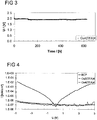
- figure 3 the stability of a device containing a 200 nm thick layer of NPB doped with Cu 4 (O 2 CCF 3 ) 4 as an example according to the invention.
- the same device as described above ( figure 2 ) was electrically stressed for 700 hours with a current of 1 mA. During the whole testing time the necessary voltage to be applied does not significantly change.
- Figure 4 shows the I-V characteristics of the same layer sequence as described before with the difference that an electron transporting material instead of a hole-transporting material is used.
- BCP is a well known electron conductor.
- the I-V characteristics of undoped BCP are shown as top most spectrum in figure 4 (diamonds).
- the conductivity of the sample drops to values around the noise level. Therefore, the p-dopants according to the present disclosure do not promote electron conductivity in typical electron conductors, particularly electron conductors based on nitrogen containing aromatic systems; they even prohibit electron conduction.
- FIG. 5A shows the I-V characteristics of eight single-carrier-devices prepared as described before by co-evaporation of NPB and the respective copper complex. Six of these compounds were fluorinated ligand L and the position and quantity of fluorine was varied to investigate the effect on doping. The last compound is non-fluorinated as a kind of reference and to show the difference beteen fluorinated and non fluorinated complexes.
- Figure 5B shows the principle of numbering of the fluorine positions on the benzoic ring of the copper-complex of the seven compounds that have been investigated.
- Each device consists of a 200nm doped organic layer sandwiched between the ITO and aluminum (150nm) electrodes.
- the NPB reference diamonds
- a first group comprises of Cu 4 (O 2 CC 6 H 5 ) 4 (squares), Cu 6 (O 2 C(2,6-F) 2 C 6 H 3 ) 6 (circles) and Cu 4 (O 2 C(4-F)C 6 H 4 ) 4 (asterisks) which all show a much lower (3 orders of magnitude) current density for positive voltages compared to NPB and no improvement (drop) of the build-in voltage (no shift towards lower voltages).
- this effect is probably due to the lack of fluorine which seems to be required for a sufficient doping effect. Even though the other two materials contain fluorine, its position and quantity seems to avoid a doping effect.
- the second compound contains two fluorine atoms on the ring on positions 2 and 6 and are thereby on the "inside” of the compound hindering the electron pulling effect of fluorine and therefore reduce the hole generation possibility on the copper atom and its doping effect.
- the third compound of this group has one fluorine atom located on position 4 which is on the "outside” of the structure, but the quantity of fluorine is to low to obtain a suitable doping effect.
- a second group comprises of four compounds with an increasing quantity of fluorine and a shift of fluorine towards the outer positions of the copper-benzoate structure.
- Cu 4 (O 2 C(3-F) C 6 H 4 ) 4 (crosses), Cu 6 (O 2 C(3,5-F) 2 C 6 H 3 ) 6 (plusses), Cu 4 (O 2 C(3,4,5-F) 3 C 6 H 2 ) 4 (dashes) and Cu 4 (O 2 C (2,3,4,5,6-F) 5 C 6 ) 4 (triangles) all have a similar behavior for positive voltages.
- the current densities with these materials doped into NPB do not drop by 3 orders of magnitude as for the first group but are within one order of magnitude compared to the NPB reference which is considered to be equivalent.
- NPB as the first reference matrix material has a HOMO level of -5.5 eV and therefore a material with a lower HOMO was chosen:
- 1-TNata (4,4',4 " -Tris(N-(1-naphthyl)-N-phenyl-amino)triphenylamine) with a HOMO of - 5.0 eV was used to prepare a similar single carrier device by coevaporation as mentioned before.
- Figure 6 shows the I-V characteristics of a single carrier device with 1-TNata doped with Cu 4 (O 2 C(2,3,4,5,6-F) 5 C 6 ) 4 (triangles) and a 1-TNata reference graph (diamonds).
- the characteristic shows an enhancement incurrent density of two orders of magnitude for positive voltages.
- the symmetrical behavior of this graph also shows the independency of the metal work functions of ITO and aluminum.
- This single carrier device shows a very clear and classical doping effect for the given matrix-dopant combination.
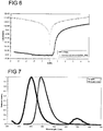
- FIG. 7 shows the photoluminescence spectrum of NPB doped with Cu 4 (O 2 CCF 3 ) 4 as an example according to the invention.
- NPB itself exhibits a blue fluorescence with a maximum around 440 nm.
- the copper complexes according to the present disclosure particularly the copper(I) trifluoroacetate complexe described before, shifts the emission of NPB towards the ultraviolet region.
- the emission maximum of NPB is shifted to around 400 nm.
- the copper(I) complexes according to the present disclosure show an emission maximum between 500 nm and 600 nm.
- Cu 2 O and an anhydride of the respective carboxylic acid in excess, for example two-fold excess with respect to a molar ratio of copper:carboxylic acid of 1:1
- a suitable solvent in excess, for example two-fold excess with respect to a molar ratio of copper:carboxylic acid of 1:1
- Cu 2 O having not reacted is removed by filtration.
- the solvent is evaporated and the obtained material heated under vacuum at elevated temperature for at least ten hours.
- the obtained material may be purified by sublimation.
- the carboxylic acid itself and water trapping material for example DEAD may be used.
- Benzoic acid (2.5 g, 10.24 mmol) was heated under nitrogen for two hours in refluxing xylenes (14 ml) in a Dean-Stark apparatus. The obtained solution was added to a copper (I) oxide (0.2 g, 1.40 mmol) and reflux was continued until all the oxide had reacted (ca. 12 hours). Upon slow cooling to room temperature, the product started to appear as a white crystalline precipitate while benzoic acid remained in the solution. After two and a half hours and thirteen minutes the solution was removed by a canula. The polycrystalline powder was washed with xylenes (3 times 20 ml) and dried under vacuum. Yield: 75%.
- Cu 4 (O 2 CCF 3 ) 4 and an at least five-fold excess of a carboxylic acid to be coordinated to the copper atoms are combined with a suitable solvent and refluxed for at least 12 hours.
- the obtained solution is evaporated to dryness and heated at elevated temperature under vacuum for several days to remove the excess of unreacted acid. Pure product may be obtained by sublimation.
- a crystalline products precipitates after the solution is allowed to cool down.
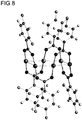
- the solids are then filtered and dried. They may contain coordinated carboxylic acids, but recrystallization from anhydrous acetone followed by drying under vacuum, as described in example 7, yields unligated non-inventive copper(II) carboxylates (see also S. I. Troyanov et al., Koord. Khimijya, 1991, vol 17, N12, 1692-1697 ).
- Figure 8 shows an X-ray structure of this compound.
- the lines between the copper atoms do not represent copper-copper bonds.
Landscapes
- Chemical & Material Sciences (AREA)
- Organic Chemistry (AREA)
- Physics & Mathematics (AREA)
- Optics & Photonics (AREA)
- Inorganic Chemistry (AREA)
- Engineering & Computer Science (AREA)
- Materials Engineering (AREA)
- Electroluminescent Light Sources (AREA)
- Organic Low-Molecular-Weight Compounds And Preparation Thereof (AREA)
- Photovoltaic Devices (AREA)
Claims (9)
- Organisches Elektronikbauelement, umfassend- ein Substrat (1),- eine erste Elektrode, die auf dem Substrat (1) angeordnet ist,- mindestens eine erste funktionelle organische Schicht, die auf der ersten Elektrode angeordnet ist, wobei die erste funktionelle Schicht eine Lochtransportschicht ist,- eine zweite Elektrode, die auf der ersten funktionellen organischen Schicht angeordnet ist,- wobei die erste funktionelle organische Schicht ein Matrixmaterial und einen p-Dotierstoff in Bezug auf das Matrixmaterial umfasst, dadurch gekennzeichnet, dass der p-Dotierstoff einen Lewis-sauren einkernigen oder mehrkernigen Kupferkomplex umfasst, der mindestens einen Liganden L mit der folgenden Formel enthält:
 - E1 und E2 gleich oder verschieden sein können und für Sauerstoff, Schwefel, Selen oder NR' stehen,- R für Wasserstoff oder einen substituierten oder unsubstituierten, verzweigten, linearen oder cyclischen Kohlenwasserstoff steht,- R' für Wasserstoff oder einen substituierten oder unsubstituierten, verzweigten, linearen oder cyclischen Kohlenwasserstoff steht, und- das Kupferatom in dem einkernigen Komplex oder mindestens ein Teil der Kupferatome des mehrkernigen Komplexes im Oxidationszustand +1 vorliegen und eine d10-Konfiguration mit abgeschlossener Schale aufweisen.
 - Organisches Elektronikbauelement gemäß dem vorhergehenden Anspruch, wobei der Kupferkomplex ein mehrkerniger Komplex ist.
- Organisches Elektronikbauelement gemäß dem vorhergehenden Anspruch, wobei mindestens ein Ligand L des Kupferkomplexes zwei Kupferatome verbrückt.
- Organisches Bauelement gemäß Anspruch 1, wobei die Gruppe R des Liganden L für eine Alkyl- und/oder Arylgruppe steht, die mindestens einen elektronenziehenden Substituenten trägt.
- Organisches Bauelement nach einem der vorherigen Ansprüche, wobei in dem Matrixmaterial der ersten funktionellen organischen Schicht eine organische Verbindung umfasst, und die organische Verbindung teilweise mit dem Kupferkomplex koordiniert.
- Organisches Bauelement nach dem vorherigen Anspruch, wobei die organische Verbindung mindestens zwei Koordinationsstellen enthält, wobei die mindestens zwei Koordinationsstellen von mindestens einem Teil der organischen Verbindung an ein Kupferatom koordinieren, um so eine Struktur mit einer Mehrzahl von Kupferkomplexen und einer Mehrzahl von Molekülen der organischen Verbindung zu bilden.
- Organisches Elektronikbauelement nach einem der vorhergehenden Ansprüche, wobei das Matrixmaterial ausgewählt ist aus einer oder mehreren Verbindungen der folgenden Gruppe bestehend aus NPB (N,N'-Bis(naphthalin-1-yl)-N,N'-bis(phenyl)-benzidin, β-NPB (N,N'-Bis(naphthalin-2-yl)-N,N'-bis(phenyl)-benzidin), TPD (N,N'-Bis(3-methylphenyl)-N,N'-bis(phenyl)-benzidin), N,N'-Bis(naphthalin-1-yl)-N,N'-bis(phenyl)-2,2-dimethylbenzidin, Spiro-TPD (N,N'-Bis(3-methylphenyl)-N,N'-bis(phenyl)-9,9-spirobifluoren), Spiro-NPB (N,N'-Bis(naphthalin-1-yl)-N,N'-bis(phenyl)-9,9-spirobifluoren), DMFL-TPD (N,N'-Bis(3-methylphenyl)-N,N'-bis(phenyl)-9,9-dimethylfluoren, DMFL-NPB (N,N'-Bis(naphthalin-1-yl)-N,N'-bis(phenyl)-9,9-dimethylfluoren), DPFL-TPD (N,N'-Bis(3-methylphenyl)-N,N'-bis(phenyl)-9,9-diphenylfluoren), DPFL-NPB (N,N'-Bis-(naphth-1-yl)-N,N'-bis(phenyl)-9,9-diphenylfluoren), Sp-TAD (2,2',7,7'-Tetrakis(n,n-diphenylamino)-9,9'-spirobifluoren), TAPC (Di-[4-(N,N-ditolylamino)-phenyl]cyclohexan), Spiro-TTB (2,2',7,7'-Tetra(N,N-ditolyl)aminospirobifluoren), BPAPF (9,9-Bis[4-(N,N-bisbiphenyl-4-yl-amino)phenyl]-9H-fluoren), Spiro-2NPB (2,2',7,7'-Tetrakis[N-naphthyl(phenyl)-amino]-9,9-spirobifluoren), Spiro-5 (2,7-Bis[N,N-bis(9,9-spirobifluoren-2-yl)-amino]-9,9-spirobifluoren), 2,2'-Spiro-DBP (2,2'-Bis-[N,N-bis(biphenyl-4-yl)amino]-9,9-spirobifluoren), PAPB (N,N'-Bis(phenanthren-9-yl)-N,N'-bis(phenyl)-benzidin), TNB (N,N,N',N'-Tetranaphthalin-2-yl-benzidin), Spiro-BPA (2,2'-Bis(N,N-diphenylamino)-9,9-spirobifluoren), NPAPF (9,9-Bis[4-(N,N-bisnaphth-2-ylamino)phenyl]-9H-fluoren), NPBAPF (9,9-Bis[4-(N,N'-bisnaphth-2-yl-N,N'-bisphenylamino)-phenyl]-9H-fluoren), TiOPC (Titanoxid-Phthalocyanin), CuPC (KupferPhthalocyanin), F4-TCNQ (2,3,5,6-Tetrafluor-7,7,8,8,-tetracyanochinodimethan), m-MTDATA (4,4',4"-Tris(N-3-methylphenyl-N-phenylamino)triphenylamin), 2T-NATA (4,4',4"-Tris(N-(naphthalin-2-yl)-N-phenylamino)triphenylamin), 1T-NATA (4,4',4"-Tris(N-(naphthalin-1-yl)-N-phenylamino)triphenylamin), NATA (4,4',4"-Tris(N,N-diphenylamino)triphenylamin), PPDN (Pyrazino[2,3-f][1,10]phenanthrolin-2,3-dicarbonitril), MeO-TPD (N,N,N',N'-Tetrakis(4-methoxyphenyl)benzidin), MeO-Spiro-TPD (2,7-Bis[N,N-bis(4-methoxyphenyl)amino]-9,9-spirobifluoren), 2,2'-MeO-Spiro-TPD (2,2'-Bis[N,N-bis(4-methoxyphenyl)amino]-9,9-spirobifluoren), β-NPP (N,N'-Di(naphthalin-2-yl)-N,N'-diphenylbenzol-1,4-diamin), NTNPB (N,N'-Diphenyl-N,N'-di-[4-(N,N-ditolylamino)phenyl]benzidin) und NPNPB (N,N'-Diphenyl-N,N'-di-[4-(N,N-diphenylamino)phenyl]benzidin).
- Organisches Elektronikbauteil nach einem der vorherigen Ansprüche, wobei das organische Elektronikbauteil ausgewählt ist aus einer Gruppe, die einen Feldeffekttransistor, eine Solarzelle, einen Photodetektor, ein optoelektronisches Bauteil, eine Licht emittierende Diode und eine Anzeige umfasst.
- Organisches Elektronikbauelement, umfassend- ein Substrat (1),- eine erste Elektrode, die auf dem Substrat (1) angeordnet ist,- mindestens eine erste funktionelle organische Schicht, die auf der ersten Elektrode angeordnet ist,- eine zweite Elektrode, die auf der ersten funktionellen organischen Schicht angeordnet ist,- wobei die erste funktionelle organische Schicht ein Matrixmaterial und einen p-Dotierstoff in Bezug auf das Matrixmaterial umfasst, dadurch gekennzeichnet, dass der p-Dotierstoff einen Lewis-sauren Kupferkomplex umfasst und das Matrixmaterial eine Lewis-basische Verbindung ist, die an die freien Koordinationsstellen der Kupferatome gemäß Schema 1 oder 2 koordiniert:


Applications Claiming Priority (2)
| Application Number | Priority Date | Filing Date | Title |
|---|---|---|---|
| US24392709P | 2009-09-18 | 2009-09-18 | |
| PCT/EP2010/063619 WO2011033023A1 (en) | 2009-09-18 | 2010-09-16 | Organic electronic device and dopant for doping an organic semiconducting matrix material |
Publications (3)
| Publication Number | Publication Date |
|---|---|
| EP2478576A1 EP2478576A1 (de) | 2012-07-25 |
| EP2478576B1 EP2478576B1 (de) | 2017-05-31 |
| EP2478576B9 true EP2478576B9 (de) | 2017-09-06 |
Family
ID=42829910
Family Applications (1)
| Application Number | Title | Priority Date | Filing Date |
|---|---|---|---|
| EP10754509.7A Active EP2478576B9 (de) | 2009-09-18 | 2010-09-16 | Organische elektronische vorrichtung und dotierstoff zur dotierung eines organischen halbleitermatrixmaterials |
Country Status (6)
| Country | Link |
|---|---|
| US (2) | US8624229B2 (de) |
| EP (1) | EP2478576B9 (de) |
| JP (1) | JP5836275B2 (de) |
| KR (1) | KR101768731B1 (de) |
| CN (1) | CN102576802B (de) |
| WO (1) | WO2011033023A1 (de) |
Families Citing this family (30)
| Publication number | Priority date | Publication date | Assignee | Title |
|---|---|---|---|---|
| DE102010013495A1 (de) * | 2010-03-31 | 2011-10-06 | Siemens Aktiengesellschaft | Dotierstoff für eine Lochleiterschicht für organische Halbleiterbauelemente und Verwendung dazu |
| DE102010062954A1 (de) | 2010-12-13 | 2012-06-14 | Osram Opto Semiconductors Gmbh | Optoelektronisches Bauelement und Verwendung eines Kupferkomplexes in einer Ladungserzeugungsschichtfolge |
| DE102010062877A1 (de) * | 2010-12-13 | 2012-06-21 | Osram Opto Semiconductors Gmbh | Organisches Lichtemittierendes Bauelement und Verwendung eines Kupferkomplexes in einer Ladungstransportschicht |
| DE102011007052A1 (de) * | 2011-04-08 | 2012-10-11 | Osram Opto Semiconductors Gmbh | Optoelektronisches Bauelement und Verwendung eines Kupferkomplexes als Dotierstoff zum Dotieren einer Schicht |
| DE102012209523A1 (de) * | 2012-06-06 | 2013-12-12 | Osram Opto Semiconductors Gmbh | Hauptgruppenmetallkomplexe als p-Dotanden für organische elektronische Matrixmaterialien |
| DE102012209520A1 (de) * | 2012-06-06 | 2013-12-12 | Osram Opto Semiconductors Gmbh | Metallkomplexe als p-Dotanden für organische elektronische Matrixmaterialien |
| DE102012211869A1 (de) | 2012-07-06 | 2014-01-09 | Osram Opto Semiconductors Gmbh | Organisches Licht emittierendes Bauelement |
| JP6239624B2 (ja) | 2012-09-18 | 2017-11-29 | メルク パテント ゲーエムベーハー | 電子素子のための材料 |
| KR102037819B1 (ko) * | 2012-12-24 | 2019-10-29 | 엘지디스플레이 주식회사 | 유기전계발광표시장치 및 그 제조방법 |
| DE102013106949A1 (de) | 2013-07-02 | 2015-01-08 | Osram Opto Semiconductors Gmbh | Optoelektronisches Bauelement, organische funktionelle Schicht und Verfahren zur Herstellung eines optoelektronischen Bauelements |
| KR102253438B1 (ko) * | 2014-03-26 | 2021-05-20 | 삼성디스플레이 주식회사 | 아민계 화합물 및 이를 포함한 유기 발광 소자 |
| EP2960315A1 (de) | 2014-06-27 | 2015-12-30 | cynora GmbH | Organische Elektrolumineszenzvorrichtung |
| WO2016012274A1 (en) | 2014-07-21 | 2016-01-28 | Basf Se | Organic-inorganic tandem solar cell |
| WO2016042070A1 (de) | 2014-09-17 | 2016-03-24 | Cynora Gmbh | Organische moleküle zur verwendung als emitter |
| DE102014114224A1 (de) | 2014-09-30 | 2016-03-31 | Osram Oled Gmbh | Organisches elektronisches Bauteil, Verwendung eines Zinkkomplexes als p-Dotierungsmittel für organische elektronische Matrixmaterialien |
| DE202014106226U1 (de) | 2014-09-30 | 2015-10-28 | Osram Oled Gmbh | Organisches elektronisches Bauteil |
| DE102015102866B4 (de) | 2015-02-27 | 2023-02-02 | Tdk Electronics Ag | Keramisches Bauelement, Bauelementanordnung und Verfahren zur Herstellung eines keramischen Bauelements |
| DE102015119778A1 (de) | 2015-11-16 | 2017-05-18 | Osram Oled Gmbh | Organisches elektronisches Bauelement, Verwendung eines p-Dotierstoffs für ein Matrixmaterial |
| DE102015121844A1 (de) * | 2015-12-15 | 2017-06-22 | Osram Oled Gmbh | Organisches elektronisches Bauelement und Verwendung eines fluorierten Sulfonimid-Metallsalzes |
| DE102016101710B4 (de) | 2016-02-01 | 2025-02-06 | Pictiva Displays International Limited | OLED und Verfahren zur Herstellung einer OLED |
| KR102534789B1 (ko) * | 2016-05-02 | 2023-05-19 | 한양대학교 산학협력단 | 과불소화산 처리된 전도성 고분자 박막의 제조방법 및 이의 용도 |
| KR102675576B1 (ko) * | 2016-07-04 | 2024-06-18 | 삼성디스플레이 주식회사 | 유기 발광 표시 장치 |
| KR102078435B1 (ko) * | 2016-07-14 | 2020-02-17 | 주식회사 엘지화학 | 유기 전계 발광 소자 및 이의 제조 방법 |
| DE102017111425A1 (de) | 2017-05-24 | 2018-11-29 | Osram Oled Gmbh | Organisches elektronisches Bauelement und Verfahren zur Herstellung eines organischen elektronischen Bauelements |
| WO2018234346A1 (en) | 2017-06-23 | 2018-12-27 | Merck Patent Gmbh | Materials for organic electroluminescent devices |
| EP3503234B1 (de) * | 2017-12-20 | 2020-11-04 | Novaled GmbH | Organische elektronische vorrichtung mit einem inversen koordinationskomplex und verfahren zur herstellung davon |
| WO2019175149A1 (en) | 2018-03-16 | 2019-09-19 | Merck Patent Gmbh | Materials for organic electroluminescent devices |
| CN114639788A (zh) * | 2020-12-15 | 2022-06-17 | 云谷(固安)科技有限公司 | 发光器件、材料筛选方法及显示面板 |
| CN113337276B (zh) * | 2021-05-10 | 2022-07-15 | 武汉大学 | 发光材料、喷墨打印薄膜光学器件的方法及其应用 |
| KR20250128345A (ko) | 2022-12-23 | 2025-08-27 | 메르크 파텐트 게엠베하 | 전자 디바이스 |
Family Cites Families (15)
| Publication number | Priority date | Publication date | Assignee | Title |
|---|---|---|---|---|
| US4622355A (en) | 1984-07-16 | 1986-11-11 | The United States Of America As Represented By The United States Department Of Energy | Radiation-hardened polymeric films |
| JPH03241778A (ja) * | 1990-02-19 | 1991-10-28 | Sekisui Chem Co Ltd | 有機太陽電池 |
| JP2998268B2 (ja) | 1991-04-19 | 2000-01-11 | 三菱化学株式会社 | 有機電界発光素子 |
| JPH11251067A (ja) | 1998-03-02 | 1999-09-17 | Junji Kido | 有機エレクトロルミネッセント素子 |
| KR20010050711A (ko) | 1999-09-29 | 2001-06-15 | 준지 키도 | 유기전계발광소자, 유기전계발광소자그룹 및 이런소자들의 발광스펙트럼의 제어방법 |
| US6764776B2 (en) | 2000-11-30 | 2004-07-20 | Semiconductor Energy Laboratory Co., Ltd. | Light emitting device |
| JP4255635B2 (ja) | 2000-11-30 | 2009-04-15 | 株式会社半導体エネルギー研究所 | 発光装置 |
| TW545080B (en) | 2000-12-28 | 2003-08-01 | Semiconductor Energy Lab | Light emitting device and method of manufacturing the same |
| DE102004010954A1 (de) * | 2004-03-03 | 2005-10-06 | Novaled Gmbh | Verwendung eines Metallkomplexes als n-Dotand für ein organisches halbleitendes Matrixmaterial, organisches Halbleitermaterial und elektronisches Bauteil |
| US7825250B2 (en) | 2004-10-01 | 2010-11-02 | Ube Industries, Ltd. | Binuclear metal complex, metal complex dye, photoelectric conversion element, and photochemical battery |
| JP4915544B2 (ja) | 2005-05-11 | 2012-04-11 | パナソニック株式会社 | 有機エレクトロルミネッセンス素子 |
| US7632703B2 (en) | 2005-12-22 | 2009-12-15 | Xerox Corporation | Organic thin-film transistors |
| JP5082423B2 (ja) * | 2006-12-14 | 2012-11-28 | ソニー株式会社 | 半導体装置及びその製造方法 |
| DE102007028236A1 (de) * | 2007-06-20 | 2009-01-02 | Siemens Ag | Halbleitendes Material und organische Gleichrichterdiode |
| US20090001360A1 (en) * | 2007-06-29 | 2009-01-01 | Masaya Nakayama | Organic el display and method for producing the same |
-
2010
- 2010-09-16 EP EP10754509.7A patent/EP2478576B9/de active Active
- 2010-09-16 KR KR1020127009765A patent/KR101768731B1/ko active Active
- 2010-09-16 WO PCT/EP2010/063619 patent/WO2011033023A1/en not_active Ceased
- 2010-09-16 CN CN201080041456.2A patent/CN102576802B/zh active Active
- 2010-09-16 JP JP2012529272A patent/JP5836275B2/ja not_active Expired - Fee Related
- 2010-09-17 US US12/884,683 patent/US8624229B2/en active Active
-
2013
- 2013-12-12 US US14/104,882 patent/US9166178B2/en active Active
Also Published As
| Publication number | Publication date |
|---|---|
| US8624229B2 (en) | 2014-01-07 |
| KR101768731B1 (ko) | 2017-08-16 |
| CN102576802A (zh) | 2012-07-11 |
| US9166178B2 (en) | 2015-10-20 |
| JP5836275B2 (ja) | 2015-12-24 |
| US20110089408A1 (en) | 2011-04-21 |
| EP2478576A1 (de) | 2012-07-25 |
| CN102576802B (zh) | 2015-08-05 |
| WO2011033023A1 (en) | 2011-03-24 |
| US20140107364A1 (en) | 2014-04-17 |
| EP2478576B1 (de) | 2017-05-31 |
| JP2013505565A (ja) | 2013-02-14 |
| KR20120080609A (ko) | 2012-07-17 |
Similar Documents
| Publication | Publication Date | Title |
|---|---|---|
| EP2478576B1 (de) | Organische elektronische vorrichtung und dotierstoff zur dotierung eines organischen halbleitermatrixmaterials | |
| KR20230169008A (ko) | 유기 전계발광 물질 및 디바이스 | |
| Wolak et al. | Functionalized pentacene derivatives for use as red emitters in organic light-emitting diodes | |
| CN107078221B (zh) | 有机电场发光元件及其制造方法 | |
| CN110662750A (zh) | 有机化合物及包含该有机化合物的有机电致发光元件 | |
| KR20130036048A (ko) | 디벤조푸란 화합물 및 8-히드록시퀴놀리노레이토 알칼리 토금속 또는 알칼리 금속 착물의 층을 포함하는 유기 전자 소자 | |
| TWI895241B (zh) | 具低lumo能量的n-雜亞芳基化合物、有機半導體層及有機電子元件 | |
| US11018310B2 (en) | Luminescent tetradentate gold(III) compounds for organic light-emitting devices and their preparation | |
| KR102032713B1 (ko) | 헤테로레프틱 이리듐 착체, 및 상기 화합물을 이용한 발광재료 및 유기 발광소자 | |
| EP3840081A1 (de) | Organische elektronische vorrichtung mit einer verbindung der formel (1), anzeigevorrichtung mit der organischen elektronischen vorrichtung sowie verbindungen der formel (1) zur verwendung in organischen elektronischen vorrichtungen | |
| EP4169092B1 (de) | Organische elektronische vorrichtung und anzeigevorrichtung mit der organischen elektronischen vorrichtung sowie zusammensetzung zur verwendung in organischen elektronischen vorrichtungen | |
| CN105009316A (zh) | 有机电场发光元件用硼化合物以及有机电场发光元件 | |
| WO2023110888A1 (en) | A ce(iv) metal complex, an organic electronic device comprising an anode layer, a cathode layer and a charge generation layer, wherein the charge generation layer comprises a p-type charge generation layer that comprises the ce(iv) metal complex and a n-type charge generation layer | |
| WO2021123067A1 (en) | Organic electronic device comprising a compound of formula (1), display device comprising the organic electronic device as well as compounds of formula (1) for use in organic electronic devices | |
| WO2009149860A2 (en) | Method of making an oled | |
| WO2020125484A1 (en) | Luminescent tetradentate ligand-containing gold (iii) compounds for organic light-emitting devices and their preparation | |
| CN105820122A (zh) | 有机电致发光材料和装置 | |
| EP3930024B1 (de) | Organische elektronische vorrichtung und anzeigevorrichtung mit der organischen elektronischen vorrichtung sowie zusammensetzung zur verwendung in organischen elektronischen vorrichtungen | |
| TW202315189A (zh) | P型半導體層的製備方法,該方法獲得之p型半導體,包含該p型半導體層的有機電子元件,包含該有機電子元件的顯示裝置、金屬化合物及該金屬化合物於該p型半導體的用途 | |
| EP4387414A1 (de) | Organische elektrolumineszenzvorrichtung mit einer verbindung der formel (i) und einer verbindung der formel (ii) und anzeigevorrichtung mit der organischen elektrolumineszenzvorrichtung | |
| Kwon et al. | Efficient blue phosphorescent host through nonbonded conformational locking interactions | |
| WO2024110651A1 (en) | Organic electroluminescent device and display device comprising the organic electroluminescent device | |
| KR102697369B1 (ko) | 두 개의 금속 도펀트를 포함한 n-도핑된 반도전성 물질 | |
| KR20260023530A (ko) | 유기 전자 장치에 사용하기 위한 화학식 (I)의 유기 화합물, 화학식 (IV)의 화합물 및 화학식 (IVa) 내지 (IVd) 중 적어도 하나의 화합물을 포함하는 조성물, 화합물 또는 조성물을 포함하는 유기 반도체층, 유기 반도체층을 포함하는 유기 전자 장치, 및 유기 전자 장치를 포함하는 디스플레이 장치 | |
| KR20230024740A (ko) | 신규한 유기전기발광 화합물 및 이를 포함하는 유기전기발광소자 |
Legal Events
| Date | Code | Title | Description |
|---|---|---|---|
| PUAI | Public reference made under article 153(3) epc to a published international application that has entered the european phase |
Free format text: ORIGINAL CODE: 0009012 |
|
| 17P | Request for examination filed |
Effective date: 20120330 |
|
| AK | Designated contracting states |
Kind code of ref document: A1 Designated state(s): AL AT BE BG CH CY CZ DE DK EE ES FI FR GB GR HR HU IE IS IT LI LT LU LV MC MK MT NL NO PL PT RO SE SI SK SM TR |
|
| DAX | Request for extension of the european patent (deleted) | ||
| 17Q | First examination report despatched |
Effective date: 20140626 |
|
| RAP1 | Party data changed (applicant data changed or rights of an application transferred) |
Owner name: OSRAM OLED GMBH |
|
| REG | Reference to a national code |
Ref country code: DE Ref legal event code: R079 Ref document number: 602010042689 Country of ref document: DE Free format text: PREVIOUS MAIN CLASS: H01L0051000000 Ipc: H01L0051540000 |
|
| GRAP | Despatch of communication of intention to grant a patent |
Free format text: ORIGINAL CODE: EPIDOSNIGR1 |
|
| INTG | Intention to grant announced |
Effective date: 20170203 |
|
| RIC1 | Information provided on ipc code assigned before grant |
Ipc: H01L 51/54 20060101AFI20170125BHEP Ipc: C07F 1/08 20060101ALI20170125BHEP |
|
| GRAS | Grant fee paid |
Free format text: ORIGINAL CODE: EPIDOSNIGR3 |
|
| GRAA | (expected) grant |
Free format text: ORIGINAL CODE: 0009210 |
|
| RIN1 | Information on inventor provided before grant (corrected) |
Inventor name: WEMKEN, JAN HAUKE Inventor name: SCHMID, GUENTER Inventor name: PETRUKHINA, MARINA A. |
|
| AK | Designated contracting states |
Kind code of ref document: B1 Designated state(s): AL AT BE BG CH CY CZ DE DK EE ES FI FR GB GR HR HU IE IS IT LI LT LU LV MC MK MT NL NO PL PT RO SE SI SK SM TR |
|
| REG | Reference to a national code |
Ref country code: CH Ref legal event code: EP Ref country code: GB Ref legal event code: FG4D |
|
| REG | Reference to a national code |
Ref country code: AT Ref legal event code: REF Ref document number: 898172 Country of ref document: AT Kind code of ref document: T Effective date: 20170615 |
|
| REG | Reference to a national code |
Ref country code: IE Ref legal event code: FG4D |
|
| REG | Reference to a national code |
Ref country code: DE Ref legal event code: R096 Ref document number: 602010042689 Country of ref document: DE |
|
| REG | Reference to a national code |
Ref country code: FR Ref legal event code: PLFP Year of fee payment: 8 |
|
| REG | Reference to a national code |
Ref country code: NL Ref legal event code: MP Effective date: 20170531 |
|
| REG | Reference to a national code |
Ref country code: LT Ref legal event code: MG4D |
|
| REG | Reference to a national code |
Ref country code: AT Ref legal event code: MK05 Ref document number: 898172 Country of ref document: AT Kind code of ref document: T Effective date: 20170531 |
|
| PG25 | Lapsed in a contracting state [announced via postgrant information from national office to epo] |
Ref country code: NO Free format text: LAPSE BECAUSE OF FAILURE TO SUBMIT A TRANSLATION OF THE DESCRIPTION OR TO PAY THE FEE WITHIN THE PRESCRIBED TIME-LIMIT Effective date: 20170831 Ref country code: GR Free format text: LAPSE BECAUSE OF FAILURE TO SUBMIT A TRANSLATION OF THE DESCRIPTION OR TO PAY THE FEE WITHIN THE PRESCRIBED TIME-LIMIT Effective date: 20170901 Ref country code: FI Free format text: LAPSE BECAUSE OF FAILURE TO SUBMIT A TRANSLATION OF THE DESCRIPTION OR TO PAY THE FEE WITHIN THE PRESCRIBED TIME-LIMIT Effective date: 20170531 Ref country code: AT Free format text: LAPSE BECAUSE OF FAILURE TO SUBMIT A TRANSLATION OF THE DESCRIPTION OR TO PAY THE FEE WITHIN THE PRESCRIBED TIME-LIMIT Effective date: 20170531 Ref country code: HR Free format text: LAPSE BECAUSE OF FAILURE TO SUBMIT A TRANSLATION OF THE DESCRIPTION OR TO PAY THE FEE WITHIN THE PRESCRIBED TIME-LIMIT Effective date: 20170531 Ref country code: ES Free format text: LAPSE BECAUSE OF FAILURE TO SUBMIT A TRANSLATION OF THE DESCRIPTION OR TO PAY THE FEE WITHIN THE PRESCRIBED TIME-LIMIT Effective date: 20170531 Ref country code: LT Free format text: LAPSE BECAUSE OF FAILURE TO SUBMIT A TRANSLATION OF THE DESCRIPTION OR TO PAY THE FEE WITHIN THE PRESCRIBED TIME-LIMIT Effective date: 20170531 |
|
| PGFP | Annual fee paid to national office [announced via postgrant information from national office to epo] |
Ref country code: GB Payment date: 20170921 Year of fee payment: 8 Ref country code: FR Payment date: 20170928 Year of fee payment: 8 |
|
| PG25 | Lapsed in a contracting state [announced via postgrant information from national office to epo] |
Ref country code: NL Free format text: LAPSE BECAUSE OF FAILURE TO SUBMIT A TRANSLATION OF THE DESCRIPTION OR TO PAY THE FEE WITHIN THE PRESCRIBED TIME-LIMIT Effective date: 20170531 Ref country code: SE Free format text: LAPSE BECAUSE OF FAILURE TO SUBMIT A TRANSLATION OF THE DESCRIPTION OR TO PAY THE FEE WITHIN THE PRESCRIBED TIME-LIMIT Effective date: 20170531 Ref country code: LV Free format text: LAPSE BECAUSE OF FAILURE TO SUBMIT A TRANSLATION OF THE DESCRIPTION OR TO PAY THE FEE WITHIN THE PRESCRIBED TIME-LIMIT Effective date: 20170531 Ref country code: BG Free format text: LAPSE BECAUSE OF FAILURE TO SUBMIT A TRANSLATION OF THE DESCRIPTION OR TO PAY THE FEE WITHIN THE PRESCRIBED TIME-LIMIT Effective date: 20170831 Ref country code: IS Free format text: LAPSE BECAUSE OF FAILURE TO SUBMIT A TRANSLATION OF THE DESCRIPTION OR TO PAY THE FEE WITHIN THE PRESCRIBED TIME-LIMIT Effective date: 20170930 |
|
| PG25 | Lapsed in a contracting state [announced via postgrant information from national office to epo] |
Ref country code: RO Free format text: LAPSE BECAUSE OF FAILURE TO SUBMIT A TRANSLATION OF THE DESCRIPTION OR TO PAY THE FEE WITHIN THE PRESCRIBED TIME-LIMIT Effective date: 20170531 Ref country code: EE Free format text: LAPSE BECAUSE OF FAILURE TO SUBMIT A TRANSLATION OF THE DESCRIPTION OR TO PAY THE FEE WITHIN THE PRESCRIBED TIME-LIMIT Effective date: 20170531 Ref country code: SK Free format text: LAPSE BECAUSE OF FAILURE TO SUBMIT A TRANSLATION OF THE DESCRIPTION OR TO PAY THE FEE WITHIN THE PRESCRIBED TIME-LIMIT Effective date: 20170531 Ref country code: CZ Free format text: LAPSE BECAUSE OF FAILURE TO SUBMIT A TRANSLATION OF THE DESCRIPTION OR TO PAY THE FEE WITHIN THE PRESCRIBED TIME-LIMIT Effective date: 20170531 Ref country code: DK Free format text: LAPSE BECAUSE OF FAILURE TO SUBMIT A TRANSLATION OF THE DESCRIPTION OR TO PAY THE FEE WITHIN THE PRESCRIBED TIME-LIMIT Effective date: 20170531 |
|
| PG25 | Lapsed in a contracting state [announced via postgrant information from national office to epo] |
Ref country code: PL Free format text: LAPSE BECAUSE OF FAILURE TO SUBMIT A TRANSLATION OF THE DESCRIPTION OR TO PAY THE FEE WITHIN THE PRESCRIBED TIME-LIMIT Effective date: 20170531 Ref country code: IT Free format text: LAPSE BECAUSE OF FAILURE TO SUBMIT A TRANSLATION OF THE DESCRIPTION OR TO PAY THE FEE WITHIN THE PRESCRIBED TIME-LIMIT Effective date: 20170531 Ref country code: SM Free format text: LAPSE BECAUSE OF FAILURE TO SUBMIT A TRANSLATION OF THE DESCRIPTION OR TO PAY THE FEE WITHIN THE PRESCRIBED TIME-LIMIT Effective date: 20170531 |
|
| REG | Reference to a national code |
Ref country code: DE Ref legal event code: R097 Ref document number: 602010042689 Country of ref document: DE |
|
| PLBE | No opposition filed within time limit |
Free format text: ORIGINAL CODE: 0009261 |
|
| STAA | Information on the status of an ep patent application or granted ep patent |
Free format text: STATUS: NO OPPOSITION FILED WITHIN TIME LIMIT |
|
| REG | Reference to a national code |
Ref country code: CH Ref legal event code: PL |
|
| 26N | No opposition filed |
Effective date: 20180301 |
|
| PG25 | Lapsed in a contracting state [announced via postgrant information from national office to epo] |
Ref country code: MC Free format text: LAPSE BECAUSE OF FAILURE TO SUBMIT A TRANSLATION OF THE DESCRIPTION OR TO PAY THE FEE WITHIN THE PRESCRIBED TIME-LIMIT Effective date: 20170531 Ref country code: SI Free format text: LAPSE BECAUSE OF FAILURE TO SUBMIT A TRANSLATION OF THE DESCRIPTION OR TO PAY THE FEE WITHIN THE PRESCRIBED TIME-LIMIT Effective date: 20170531 |
|
| REG | Reference to a national code |
Ref country code: IE Ref legal event code: MM4A |
|
| REG | Reference to a national code |
Ref country code: BE Ref legal event code: MM Effective date: 20170930 |
|
| PG25 | Lapsed in a contracting state [announced via postgrant information from national office to epo] |
Ref country code: LU Free format text: LAPSE BECAUSE OF NON-PAYMENT OF DUE FEES Effective date: 20170916 |
|
| PG25 | Lapsed in a contracting state [announced via postgrant information from national office to epo] |
Ref country code: LI Free format text: LAPSE BECAUSE OF NON-PAYMENT OF DUE FEES Effective date: 20170930 Ref country code: CH Free format text: LAPSE BECAUSE OF NON-PAYMENT OF DUE FEES Effective date: 20170930 Ref country code: IE Free format text: LAPSE BECAUSE OF NON-PAYMENT OF DUE FEES Effective date: 20170916 |
|
| PG25 | Lapsed in a contracting state [announced via postgrant information from national office to epo] |
Ref country code: BE Free format text: LAPSE BECAUSE OF NON-PAYMENT OF DUE FEES Effective date: 20170930 |
|
| PG25 | Lapsed in a contracting state [announced via postgrant information from national office to epo] |
Ref country code: MT Free format text: LAPSE BECAUSE OF NON-PAYMENT OF DUE FEES Effective date: 20170916 |
|
| GBPC | Gb: european patent ceased through non-payment of renewal fee |
Effective date: 20180916 |
|
| PG25 | Lapsed in a contracting state [announced via postgrant information from national office to epo] |
Ref country code: HU Free format text: LAPSE BECAUSE OF FAILURE TO SUBMIT A TRANSLATION OF THE DESCRIPTION OR TO PAY THE FEE WITHIN THE PRESCRIBED TIME-LIMIT; INVALID AB INITIO Effective date: 20100916 |
|
| PG25 | Lapsed in a contracting state [announced via postgrant information from national office to epo] |
Ref country code: FR Free format text: LAPSE BECAUSE OF NON-PAYMENT OF DUE FEES Effective date: 20180930 |
|
| PG25 | Lapsed in a contracting state [announced via postgrant information from national office to epo] |
Ref country code: GB Free format text: LAPSE BECAUSE OF NON-PAYMENT OF DUE FEES Effective date: 20180916 Ref country code: CY Free format text: LAPSE BECAUSE OF NON-PAYMENT OF DUE FEES Effective date: 20170531 |
|
| PG25 | Lapsed in a contracting state [announced via postgrant information from national office to epo] |
Ref country code: MK Free format text: LAPSE BECAUSE OF FAILURE TO SUBMIT A TRANSLATION OF THE DESCRIPTION OR TO PAY THE FEE WITHIN THE PRESCRIBED TIME-LIMIT Effective date: 20170531 |
|
| PG25 | Lapsed in a contracting state [announced via postgrant information from national office to epo] |
Ref country code: TR Free format text: LAPSE BECAUSE OF FAILURE TO SUBMIT A TRANSLATION OF THE DESCRIPTION OR TO PAY THE FEE WITHIN THE PRESCRIBED TIME-LIMIT Effective date: 20170531 |
|
| PG25 | Lapsed in a contracting state [announced via postgrant information from national office to epo] |
Ref country code: PT Free format text: LAPSE BECAUSE OF FAILURE TO SUBMIT A TRANSLATION OF THE DESCRIPTION OR TO PAY THE FEE WITHIN THE PRESCRIBED TIME-LIMIT Effective date: 20170531 |
|
| PG25 | Lapsed in a contracting state [announced via postgrant information from national office to epo] |
Ref country code: AL Free format text: LAPSE BECAUSE OF FAILURE TO SUBMIT A TRANSLATION OF THE DESCRIPTION OR TO PAY THE FEE WITHIN THE PRESCRIBED TIME-LIMIT Effective date: 20170531 |
|
| REG | Reference to a national code |
Ref country code: DE Ref legal event code: R079 Ref document number: 602010042689 Country of ref document: DE Free format text: PREVIOUS MAIN CLASS: H01L0051540000 Ipc: H10K0085000000 |
|
| PGFP | Annual fee paid to national office [announced via postgrant information from national office to epo] |
Ref country code: DE Payment date: 20250925 Year of fee payment: 16 |
|
| REG | Reference to a national code |
Ref country code: DE Ref legal event code: R081 Ref document number: 602010042689 Country of ref document: DE Owner name: AMS-OSRAM INTERNATIONAL GMBH, DE Free format text: FORMER OWNER: OSRAM OLED GMBH, 93049 REGENSBURG, DE |