EP2475233B1 - System zur Ablagerung von Mikrodraht - Google Patents
System zur Ablagerung von Mikrodraht Download PDFInfo
- Publication number
- EP2475233B1 EP2475233B1 EP12150324.7A EP12150324A EP2475233B1 EP 2475233 B1 EP2475233 B1 EP 2475233B1 EP 12150324 A EP12150324 A EP 12150324A EP 2475233 B1 EP2475233 B1 EP 2475233B1
- Authority
- EP
- European Patent Office
- Prior art keywords
- microwire
- dielectric
- printing
- trace
- dielectric layer
- Prior art date
- Legal status (The legal status is an assumption and is not a legal conclusion. Google has not performed a legal analysis and makes no representation as to the accuracy of the status listed.)
- Active
Links
Images




Classifications
-
- H—ELECTRICITY
- H05—ELECTRIC TECHNIQUES NOT OTHERWISE PROVIDED FOR
- H05K—PRINTED CIRCUITS; CASINGS OR CONSTRUCTIONAL DETAILS OF ELECTRIC APPARATUS; MANUFACTURE OF ASSEMBLAGES OF ELECTRICAL COMPONENTS
- H05K1/00—Printed circuits
- H05K1/02—Details
-
- H—ELECTRICITY
- H05—ELECTRIC TECHNIQUES NOT OTHERWISE PROVIDED FOR
- H05K—PRINTED CIRCUITS; CASINGS OR CONSTRUCTIONAL DETAILS OF ELECTRIC APPARATUS; MANUFACTURE OF ASSEMBLAGES OF ELECTRICAL COMPONENTS
- H05K13/00—Apparatus or processes specially adapted for manufacturing or adjusting assemblages of electric components
- H05K13/06—Wiring by machine
-
- H—ELECTRICITY
- H05—ELECTRIC TECHNIQUES NOT OTHERWISE PROVIDED FOR
- H05K—PRINTED CIRCUITS; CASINGS OR CONSTRUCTIONAL DETAILS OF ELECTRIC APPARATUS; MANUFACTURE OF ASSEMBLAGES OF ELECTRICAL COMPONENTS
- H05K3/00—Apparatus or processes for manufacturing printed circuits
- H05K3/10—Apparatus or processes for manufacturing printed circuits in which conductive material is applied to the insulating support in such a manner as to form the desired conductive pattern
- H05K3/103—Apparatus or processes for manufacturing printed circuits in which conductive material is applied to the insulating support in such a manner as to form the desired conductive pattern by bonding or embedding conductive wires or strips
-
- H—ELECTRICITY
- H05—ELECTRIC TECHNIQUES NOT OTHERWISE PROVIDED FOR
- H05K—PRINTED CIRCUITS; CASINGS OR CONSTRUCTIONAL DETAILS OF ELECTRIC APPARATUS; MANUFACTURE OF ASSEMBLAGES OF ELECTRICAL COMPONENTS
- H05K1/00—Printed circuits
- H05K1/02—Details
- H05K1/0213—Electrical arrangements not otherwise provided for
- H05K1/0237—High frequency adaptations
- H05K1/0245—Lay-out of balanced signal pairs, e.g. differential lines or twisted lines
-
- H—ELECTRICITY
- H05—ELECTRIC TECHNIQUES NOT OTHERWISE PROVIDED FOR
- H05K—PRINTED CIRCUITS; CASINGS OR CONSTRUCTIONAL DETAILS OF ELECTRIC APPARATUS; MANUFACTURE OF ASSEMBLAGES OF ELECTRICAL COMPONENTS
- H05K2201/00—Indexing scheme relating to printed circuits covered by H05K1/00
- H05K2201/09—Shape and layout
- H05K2201/09209—Shape and layout details of conductors
- H05K2201/09218—Conductive traces
- H05K2201/09236—Parallel layout
-
- H—ELECTRICITY
- H05—ELECTRIC TECHNIQUES NOT OTHERWISE PROVIDED FOR
- H05K—PRINTED CIRCUITS; CASINGS OR CONSTRUCTIONAL DETAILS OF ELECTRIC APPARATUS; MANUFACTURE OF ASSEMBLAGES OF ELECTRICAL COMPONENTS
- H05K2201/00—Indexing scheme relating to printed circuits covered by H05K1/00
- H05K2201/10—Details of components or other objects attached to or integrated in a printed circuit board
- H05K2201/10227—Other objects, e.g. metallic pieces
- H05K2201/10287—Metal wires as connectors or conductors
-
- H—ELECTRICITY
- H05—ELECTRIC TECHNIQUES NOT OTHERWISE PROVIDED FOR
- H05K—PRINTED CIRCUITS; CASINGS OR CONSTRUCTIONAL DETAILS OF ELECTRIC APPARATUS; MANUFACTURE OF ASSEMBLAGES OF ELECTRICAL COMPONENTS
- H05K2203/00—Indexing scheme relating to apparatus or processes for manufacturing printed circuits covered by H05K3/00
- H05K2203/15—Position of the PCB during processing
- H05K2203/1545—Continuous processing, i.e. involving rolls moving a band-like or solid carrier along a continuous production path
-
- H—ELECTRICITY
- H05—ELECTRIC TECHNIQUES NOT OTHERWISE PROVIDED FOR
- H05K—PRINTED CIRCUITS; CASINGS OR CONSTRUCTIONAL DETAILS OF ELECTRIC APPARATUS; MANUFACTURE OF ASSEMBLAGES OF ELECTRICAL COMPONENTS
- H05K3/00—Apparatus or processes for manufacturing printed circuits
- H05K3/38—Improvement of the adhesion between the insulating substrate and the metal
- H05K3/386—Improvement of the adhesion between the insulating substrate and the metal by the use of an organic polymeric bonding layer, e.g. adhesive
-
- H—ELECTRICITY
- H05—ELECTRIC TECHNIQUES NOT OTHERWISE PROVIDED FOR
- H05K—PRINTED CIRCUITS; CASINGS OR CONSTRUCTIONAL DETAILS OF ELECTRIC APPARATUS; MANUFACTURE OF ASSEMBLAGES OF ELECTRICAL COMPONENTS
- H05K3/00—Apparatus or processes for manufacturing printed circuits
- H05K3/46—Manufacturing multilayer circuits
- H05K3/4644—Manufacturing multilayer circuits by building the multilayer layer by layer, i.e. build-up multilayer circuits
- H05K3/4664—Adding a circuit layer by thick film methods, e.g. printing techniques or by other techniques for making conductive patterns by using pastes, inks or powders
-
- Y—GENERAL TAGGING OF NEW TECHNOLOGICAL DEVELOPMENTS; GENERAL TAGGING OF CROSS-SECTIONAL TECHNOLOGIES SPANNING OVER SEVERAL SECTIONS OF THE IPC; TECHNICAL SUBJECTS COVERED BY FORMER USPC CROSS-REFERENCE ART COLLECTIONS [XRACs] AND DIGESTS
- Y10—TECHNICAL SUBJECTS COVERED BY FORMER USPC
- Y10T—TECHNICAL SUBJECTS COVERED BY FORMER US CLASSIFICATION
- Y10T29/00—Metal working
- Y10T29/53—Means to assemble or disassemble
- Y10T29/5313—Means to assemble electrical device
- Y10T29/532—Conductor
-
- Y—GENERAL TAGGING OF NEW TECHNOLOGICAL DEVELOPMENTS; GENERAL TAGGING OF CROSS-SECTIONAL TECHNOLOGIES SPANNING OVER SEVERAL SECTIONS OF THE IPC; TECHNICAL SUBJECTS COVERED BY FORMER USPC CROSS-REFERENCE ART COLLECTIONS [XRACs] AND DIGESTS
- Y10—TECHNICAL SUBJECTS COVERED BY FORMER USPC
- Y10T—TECHNICAL SUBJECTS COVERED BY FORMER US CLASSIFICATION
- Y10T29/00—Metal working
- Y10T29/53—Means to assemble or disassemble
- Y10T29/5313—Means to assemble electrical device
- Y10T29/532—Conductor
- Y10T29/53209—Terminal or connector
- Y10T29/53213—Assembled to wire-type conductor
Definitions
- Embodiments of the disclosure relate generally to the field of electronic circuits and more particularly to embodiments for depositing dielectric and conductive materials in combination with microwire conductors for electrical circuits.
- US 4000558 discloses a known process of fabricating a wiring harness wherein an uninsulated wire is placed on a bottom layer of dielectric material and a top layer of dielectric material is provided to insulate the wire.
- GB2161325 dicsloses a known method of making wire scribed circuit boards.
- US 6831371 discloses a known integrated circuit substrate having embedded wire conductors and method therefore.
- Exemplary embodiments provide a microcircuit deposition system which incorporates a first printing engine for depositing a dielectric on a substrate.
- a microwire spooling machine houses a microwire spool and incorporates a tension guide to position a microwire trace onto the dielectric layer.
- a second printing engine trails the microwire spooling machine to deposit a covering dielectric layer over the microwire trace.
- the embodiments described herein demonstrate a system for controlled installation of thin, uninsulated copper wire of less than 100 micrometers (about 38 gauge or less) in diameter (microwire) onto various substrates including composite skins, subsystem enclosures, and supporting structures on platforms where there is a desire to reduce discrete wiring.
- a spooling machine places the microwire onto the substrate with a control tip, and a direct-write deposition system will both precede and follow the tooltip to print dielectric material for insulating the microwire and conducting material where needed to bridge the microwire with other traces or circuit elements.
- FIG. 1 shows an exemplary embodiment of a deposition system employing a first printing engine 10 for depositing a dielectric or insulating layer 12 on a substrate 14.
- a microwire spooling machine 16 houses microwire spools 18 and employs a tensioning guide 20 to position a microwire trace 22 onto the dielectric layer.
- the spooling machine may be mechanically or controllably connected to track the first printing engine at a desired distance.
- the microwire trace may be deposited onto the dielectric layer while still tacky from printing to provide an adhesive effect in constraining the microwire trace.
- a cutter 24 severs the microwire trace at a desired length.
- a second printing engine 26 trails the microwire spooling machine to deposit a covering dielectric or insulating layer 28.
- the second printing engine may be mechanically or controllably connected to track the first printing engine at a desired distance.
- dielectric layer 12 as deposited on substrate 14 provides an insulating path as shown in FIG. 2A for segregation of the microwire trace from the surface of the substrate which may be a composite, titanium, aluminum or alternative material surface associated either with a system-in-a-package (SIP) integrated circuit, other printed circuit element or an operational surface such as an unmanned aerial vehicle (UAV) skin.
- the dielectric layer incorporates Polyvinylbutyral (PVB) materials.
- Microwire trace 22 deposited on the dielectric layer 12 as shown in FIG. 2B provides a high conductivity trace with superior mechanical properties to a printed conductive trace.
- a silver ink printed trace of 1 m in length has a resistance of approximately 1 k ⁇ .
- R total resistance
- p the resistivity (1.68x10 -8 ⁇ m for Cu)
- 1 the length of the trace (1 m)
- A is the cross sectional area of the trace (8x10 -9 m2 for exemplary 38 gauge microwire)
- a total resistance of 2.1 ⁇ is provided for a 1 m trace.
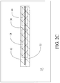
- Deposition of the covering dielectric layer 28 as shown in FIG. 2C provides top insulation for the microwire trace as well as additional adhesive capability to restrain the microwire.
- a printing gap 30 is shown in the covering dielectric layer representative of the capability in the system to provide cross connection with subsequently printed traces of silver ink or similar materials or other micro wire traces for cross connection traces or circuits. While shown for the covering layer, similar printing gaps may be employed in the initial dielectric layer for circuit interconnection with lower layers of conductive materials on the substrate thereby enabling stacked electronic circuits.
- the system may also employ one or more ultraviolet (UV) curing elements 32 as shown in FIG. 1 tracking the spooling machine and second printing engine for curing after printing of dielectric layers employing a UV sensitive polymer as a portion of the dielectric layer composition.
- UV ultraviolet
- Microwire spooling machine 16 An exemplary arrangement for the Microwire spooling machine 16 shown in FIG. 3 .
- Microwire of small gage approximately 38 or 40 (100.838 ⁇ m or 79.756 ⁇ m respectively) is held in a dispensing spool 18 from which the microwire is drawn and fed through a set of feed rollers 42.
- a guide bale 44 or similar structure orients and guides the microwire for placement onto the substrate or dielectric covering layer with tensioning guide 20.
- a cutter 24 is provided to severe the wire at the termination of a trace. For the embodiment shown, the cutter operates transversely to allow a micro wire tail 46 to extend from the guide bale.
- a positioning foot 48 is moveable vertically in a telescoping fitting 50 to engage and urge the tail into surface contact.
- Roller mounting of fitting 50 horizontally in track 52 allows controlled lateral motion of the foot to maintain contact of the tail during initial lateral motion of the spooling machine for sufficient adherence to the surface of the dielectric layer 12 to maintain position.
- the foot is then withdrawn and the guide bale and tensioning guide then maintain sufficient tension in the microwire trace as deposited to provide the desired linearity of the trace.
- the embodiment described provides a process as shown in FIG. 4 for creating circuits by deposition of a first dielectric or insulating layer on a substrate using a direct printing process, step 402.
- a microwire is then unspooled and deposited onto the dielectric layer, step 404, which may adhesively bind the wire.
- UV curing is then applied to dry the insulating layer and adhesive, step 406.
- a second dielectric or insulating layer is then deposited over the microwire with a direct printing process, step 408, with circuit interconnection gapping by suspension of printing feed at predetermined locations, step 410.
- UV curing of the second insulating layer is then accomplished, step 412.
- direct printing of conducting ink for circuit interconnection through the second layer gapping is then employed, step 414.
- a first printing engine for interruptibly depositing a dielectric with a UV sensitive polymer base on a substrate
- a microwire spooling machine connected to track the first printing engine and housing a microwire spool and incorporating a tension guide to position a microwire trace onto the dielectric layer, said microwire drawn from the spool and fed through a set of feed rollers and wherein the microwire trace is deposited onto the dielectric layer while still tacky from printing to provide an adhesive effect in constraining the microwire trace
- said spooling machine further incorporating a guide bale to orient and guide the microwire from the feed rollers for placement onto the dielectric, a tensioning guide to provide the desired linearity of the trace and a cutter to sever the microwire trace at a desired length
- a UV source connected to track the spooling machine for curing of the dielectric layer with adhered microwire trace
- a second printing engine connected to
Landscapes
- Engineering & Computer Science (AREA)
- Microelectronics & Electronic Packaging (AREA)
- Manufacturing & Machinery (AREA)
- Manufacturing Of Printed Wiring (AREA)
- Non-Metallic Protective Coatings For Printed Circuits (AREA)
- Printing Methods (AREA)
Claims (19)
- Mikroschaltungs-Ablagerungssystem mit:einer ersten Druckmaschine (10) zum Ablagern eines Dielektrikums (12) auf einem Substrat (14);einer Mikrodraht-Spulmaschine (16), wobei der Mikrodraht ein nicht isolierter Draht mit einem Durchmesser von weniger als 100 Mikrometern ist, wobei in der Spulmaschine eine Mikrodrahtspule (18) untergebracht und eine Zugführung (20) enthalten ist, um eine Mikrodraht-Leiterbahn (22) auf der Dielektrikumsschicht (12) zu positionieren;einer zweiten Druckmaschine (26), die der Mikrodraht-Spulmaschine (16) nachfolgt, um eine Dielektrikums-Deckschicht (28) über der Mikrodraht-Leiterbahn (22) abzulagern.
- Mikroschaltungs-Ablagerungssystem nach Anspruch 1, das des Weiteren eine Schneidvorrichtung (24) aufweist, um die Mikrodraht-Leiterbahn (22) bei der gewünschten Länge abzuschneiden.
- Mikroschaltungs-Ablagerungssystem nach Anspruch 1, wobei das System dazu ausgelegt ist, die Mikrodraht-Leiterbahn (22) auf der Dielektrikumsschicht (12) abzulagern, während sie noch vom Drucken klebend ist, um eine Klebewirkung beim Festlegen der Mikrodraht-Leiterbahn (22) vorzusehen.
- Mikroschaltungs-Ablagerungssystem nach Anspruch 1, wobei das gedruckte Dielektrikum (12) UV-empfindlich ist und das System des Weiteren wenigstens eine Ultraviolett(UV)-Quelle (32) nach einer der Druckmaschinen (10, 26) aufweist, um das Dielektrikum (12) auszuhärten.
- Mikroschaltungs-Ablagerungssystem nach Anspruch 1, wobei das System dazu ausgelegt ist, den Mikrodraht (22) von der Spule (18) zu ziehen und den Mikrodraht durch einen Satz von Zuführrollen zuzuführen.
- Mikroschaltungs-Ablagerungssystem nach Anspruch 5, das des Weiteren einen Führungsbügel (44) aufweist, um den Mikrodraht (22) auszurichten und von den Zuführrollen (42) zur Platzierung auf das Dielektrikum (12) zu führen.
- Mikroschaltungs-Ablagerungssystem nach Anspruch 3, das des Weiteren eine Zugführung (20) aufweist, um die gewünschte Linearität der Leiterbahn (22) vorzusehen.
- Mikroschaltungs-Ablagerungssystem nach Anspruch 1, wobei die erste und die zweite Druckmaschine (10, 26) unterbrechbar sind, um Verbindungslücken in der Dielektrikumsschicht (12) und der Dielektrikums-Deckschicht (28) zu bilden.
- Mikrodrahtschaltung mit:einer ersten Dielektrikumsschicht (12), die auf ein Substrat (14) mit einem Direktschreibsystem gedruckt ist;einer gezogenen Mikrodraht-Leiterbahn, wobei der Mikrodraht ein nicht isolierter Draht mit einem Durchmesser von weniger als 100 Mikrometern ist, der auf der Dielektrikumsschicht (12) positioniert und daran geklebt ist; undeiner zweiten Dielektrikumsschicht (28), die mit einem Direktschreibsystem über die gezogene Mikrodraht-Leiterbahn (22) gedruckt ist.
- Mikrodrahtschaltung nach Anspruch 9, wobei die zweite Dielektrikumsschicht (28) Verbindungslücken im Direktschreibdruck aufweist.
- Mikrodrahtschaltung nach Anspruch 9 oder 10, wobei die erste Dielektrikumsschicht (12) Verbindungslücken im Direktschreibdruck aufweist.
- Mikrodrahtschaltung nach Anspruch 9, 10 oder 11, wobei das Substrat (14) eine Komposithaut aufweist.
- Mikrodrahtschaltung nach Anspruch 12, wobei die Komposithaut die Haut eines unbemannten Fluggeräts (unmanned aerial vehicle; UAV) ist.
- Verfahren zum Anbringen eines Mikrodrahts, wobei der Mikrodraht ein nicht isolierter Draht mit einem Durchmesser von weniger als 100 Mikrometern ist, wobei das Verfahren umfasst:Drucken einer Bodenschicht aus einem dielektrischen Material (12), um einen gezogenen Mikrodraht (22) von einem Substratmaterial (14) zu isolieren;Platzieren des gezogenen Mikrodrahts (22) auf der Schicht des dielektrischen Materials (12); undDrucken einer Oberschicht (28) des dielektrischen Materials, um den gezogenen Mikrodraht (22) von der Umgebung zu isolieren.
- Verfahren zum Anbringen eines Mikrodrahts (22) nach Anspruch 14, das des Weiteren das Anwenden von UV-Härten umfasst, um die Dielektrikums-Bodenschicht (12) zu trocknen.
- Verfahren zum Anbringen eines Mikrodrahts (22) nach Anspruch 14 oder 15, das des Weiteren das Anwenden von UV-Härten umfasst, um die Dielektrikums-Oberschicht (28) zu trocknen.
- Verfahren zum Anbringen eines Mikrodrahts (22) nach Anspruch 14 bis 16, wobei das Drucken einer Oberschicht (28) das Vorsehen von Lücken an vorgegebenen Stellen zur Schaltungsverbindung umfasst.
- Verfahren zum Anbringen eines Mikrodrahts (22) nach Anspruch 14 bis 17, wobei das Drucken einer Bodenschicht (12) das Vorsehen von Lücken an vorgegebenen Stellen zur Schaltungsverbindung umfasst.
- Verfahren zum Anbringen eines Mikrodrahts (22) nach Anspruch 17, das des Weiteren das direkte Drucken von leitfähiger Tinte zur Schaltungsverbindung durch die Oberschicht-Lücken umfasst.
Applications Claiming Priority (1)
| Application Number | Priority Date | Filing Date | Title |
|---|---|---|---|
| US12/985,247 US8635767B2 (en) | 2011-01-05 | 2011-01-05 | System for depositing microwire |
Publications (2)
| Publication Number | Publication Date |
|---|---|
| EP2475233A1 EP2475233A1 (de) | 2012-07-11 |
| EP2475233B1 true EP2475233B1 (de) | 2013-12-04 |
Family
ID=45562707
Family Applications (1)
| Application Number | Title | Priority Date | Filing Date |
|---|---|---|---|
| EP12150324.7A Active EP2475233B1 (de) | 2011-01-05 | 2012-01-05 | System zur Ablagerung von Mikrodraht |
Country Status (4)
| Country | Link |
|---|---|
| US (3) | US8635767B2 (de) |
| EP (1) | EP2475233B1 (de) |
| JP (1) | JP5889623B2 (de) |
| CN (1) | CN102595791B (de) |
Families Citing this family (4)
| Publication number | Priority date | Publication date | Assignee | Title |
|---|---|---|---|---|
| GB2502600B8 (en) | 2012-05-31 | 2015-01-07 | Improvements in touch sensitive displays | |
| WO2019161256A2 (en) | 2018-02-15 | 2019-08-22 | The Charles Stark Draper Laboratory, Inc. | Electrostatic motor |
| CN109731622B (zh) * | 2018-12-30 | 2022-01-07 | 深圳博华仕科技有限公司 | 一种微流控芯片的电极印造装置及印造方法 |
| CN115038251B (zh) * | 2022-07-20 | 2024-02-02 | 江南大学 | 一种利用基于金属丝的直书写工艺制作传感器的方法 |
Family Cites Families (27)
| Publication number | Priority date | Publication date | Assignee | Title |
|---|---|---|---|---|
| US3547718A (en) * | 1967-05-18 | 1970-12-15 | Rogers Corp | Method of making flat flexible electrical cables |
| US3674602A (en) * | 1969-10-09 | 1972-07-04 | Photocircuits Corp | Apparatus for making wire scribed circuit boards |
| US3808042A (en) * | 1970-06-05 | 1974-04-30 | Owens Illinois Inc | Multilayer dielectric |
| US4000558A (en) | 1971-10-14 | 1977-01-04 | International Telephone And Telegraph Corporation | Process of fabricating wiring harness |
| US4416914A (en) * | 1980-12-29 | 1983-11-22 | General Electric Company | Electrical conductors arranged in multiple layers and preparation thereof |
| US4427478A (en) | 1982-06-28 | 1984-01-24 | International Business Machines Corporation | Process for making an encapsulated circuit board and products made thereby |
| EP0168602A1 (de) | 1984-06-25 | 1986-01-22 | Kollmorgen Technologies Corporation | Methode zur Herstellung von Verbindungsschaltungsplatten |
| US4689270A (en) * | 1984-07-20 | 1987-08-25 | W. C. Heraeus Gmbh | Composite substrate for printed circuits and printed circuit-substrate combination |
| US5035939A (en) * | 1989-08-31 | 1991-07-30 | David Sarnoff Research Center, Inc. | Manufacture of printed circuit boards |
| JPH05226815A (ja) * | 1992-02-12 | 1993-09-03 | Fujitsu Ltd | ワイヤ位置決め装置 |
| JPH06275949A (ja) * | 1993-03-18 | 1994-09-30 | Hitachi Chem Co Ltd | 配線板の製造法及び装置 |
| JPH09107169A (ja) * | 1995-10-13 | 1997-04-22 | Yazaki Corp | シート配線板の製造方法 |
| JPH11163499A (ja) * | 1997-11-28 | 1999-06-18 | Nitto Boseki Co Ltd | プリント配線板の製造方法及びこの製造方法によるプリント配線板 |
| US6000120A (en) * | 1998-04-16 | 1999-12-14 | Motorola, Inc. | Method of making coaxial transmission lines on a printed circuit board |
| JP3255118B2 (ja) * | 1998-08-04 | 2002-02-12 | 株式会社村田製作所 | 伝送線路および伝送線路共振器 |
| US20050156991A1 (en) | 1998-09-30 | 2005-07-21 | Optomec Design Company | Maskless direct write of copper using an annular aerosol jet |
| US7045015B2 (en) | 1998-09-30 | 2006-05-16 | Optomec Design Company | Apparatuses and method for maskless mesoscale material deposition |
| CA2363409A1 (en) * | 2001-11-20 | 2003-05-20 | Microbonds, Inc. | A wire bonder for ball bonding insulated wire and method of using same |
| US6831371B1 (en) | 2002-03-16 | 2004-12-14 | Amkor Technology, Inc. | Integrated circuit substrate having embedded wire conductors and method therefor |
| US7709766B2 (en) | 2002-08-05 | 2010-05-04 | Research Foundation Of The State University Of New York | System and method for manufacturing embedded conformal electronics |
| ATE396790T1 (de) | 2002-12-17 | 2008-06-15 | Univ New York State Res Found | Direkter auftrag von metallischen leitermustern auf isolierflächen |
| US20040258841A1 (en) * | 2003-06-19 | 2004-12-23 | Casey John F. | Methods for depositing a thickfilm dielectric on a substrate |
| US20050156693A1 (en) * | 2004-01-20 | 2005-07-21 | Dove Lewis R. | Quasi-coax transmission lines |
| US7646015B2 (en) * | 2006-10-31 | 2010-01-12 | Semiconductor Energy Laboratory Co., Ltd. | Manufacturing method of semiconductor device and semiconductor device |
| TWI336782B (en) * | 2007-07-05 | 2011-02-01 | Apex Biotechnology Corp | Composite modified electrode trip |
| KR101042200B1 (ko) * | 2010-09-02 | 2011-06-16 | 드림스페이스월드주식회사 | Pcb를 사용한 무인 비행체 |
| EP3019641A4 (de) * | 2013-07-09 | 2017-07-19 | United Technologies Corporation | Luftfahrtkomponenten aus einem beschichteten polymer |
-
2011
- 2011-01-05 US US12/985,247 patent/US8635767B2/en active Active
- 2011-12-09 JP JP2011270137A patent/JP5889623B2/ja active Active
-
2012
- 2012-01-05 EP EP12150324.7A patent/EP2475233B1/de active Active
- 2012-01-05 CN CN201210012032.4A patent/CN102595791B/zh active Active
-
2013
- 2013-12-19 US US14/134,028 patent/US9258901B2/en active Active
-
2015
- 2015-11-11 US US14/938,444 patent/US10863614B2/en active Active
Also Published As
| Publication number | Publication date |
|---|---|
| JP2012156492A (ja) | 2012-08-16 |
| CN102595791B (zh) | 2017-04-12 |
| CN102595791A (zh) | 2012-07-18 |
| US10863614B2 (en) | 2020-12-08 |
| US8635767B2 (en) | 2014-01-28 |
| US9258901B2 (en) | 2016-02-09 |
| JP5889623B2 (ja) | 2016-03-22 |
| US20160066407A1 (en) | 2016-03-03 |
| US20140102769A1 (en) | 2014-04-17 |
| EP2475233A1 (de) | 2012-07-11 |
| US20120168204A1 (en) | 2012-07-05 |
Similar Documents
| Publication | Publication Date | Title |
|---|---|---|
| US11116070B2 (en) | Interconnect circuit methods and devices | |
| US10863614B2 (en) | Microwire circuit and deposition system | |
| CN102026529A (zh) | 屏蔽膜、具有该屏蔽膜的屏蔽配线板、屏蔽膜的接地方法 | |
| JP2009038278A (ja) | プリント配線板用シールドフィルム及びプリント配線板 | |
| JP2005506901A (ja) | 電子部品堆積用テープ組成物 | |
| JP2000269632A (ja) | シールドフレキシブルプリント配線板の製造方法、シールドフレキシブルプリント配線板用補強シールドフィルム及びシールドフレキシブルプリント配線板 | |
| CN106205954A (zh) | 电感器及其形成方法 | |
| JP6148176B2 (ja) | フレキシブル基板上に電気構成要素を組み立てる方法および装置、ならびに電気構成要素とフレキシブル基板との組立体 | |
| KR101416581B1 (ko) | 알루미늄 패턴을 이용한 디지타이저 기판 및 이의 제조방법 | |
| WO2016063907A1 (ja) | フィルム状プリント回路板及びその製造方法 | |
| EP3648119A1 (de) | Elektrische vorrichtung für fahrzeug | |
| EP3664587B1 (de) | Elektronische vorrichtung und herstellungsverfahren dafür | |
| CN204230234U (zh) | 配线部件 | |
| JP2012156492A5 (de) | ||
| CN103021878B (zh) | 用于形成电子模块的方法及系统 | |
| EP3219177B1 (de) | Flexible schaltung mit partiellem bodenpfad | |
| EP3001783A1 (de) | In eine komponente eingebettetes substrat und verfahren zur herstellung davon | |
| US9723726B2 (en) | Film composite having electrical functionality for applying to a substrate | |
| WO2019151434A1 (ja) | 部材接続方法及び接着テープ | |
| US10020250B2 (en) | Interposer, module, and method of producing interposer | |
| CN1816250A (zh) | 电子部件安装基板 | |
| KR102423487B1 (ko) | 플렉시블 플랫 케이블의 제조방법 및 이를 통해 제조된 플렉시블 플랫 케이블 | |
| KR101408097B1 (ko) | 임피던스 매칭용 시트 및 그를 이용한 연성 플랫 케이블의 제조방법 | |
| JP6205814B2 (ja) | 配線基体およびその製造方法 | |
| JP2015012096A (ja) | 多層プリント配線板の製造方法及び接着シート |
Legal Events
| Date | Code | Title | Description |
|---|---|---|---|
| PUAI | Public reference made under article 153(3) epc to a published international application that has entered the european phase |
Free format text: ORIGINAL CODE: 0009012 |
|
| 17P | Request for examination filed |
Effective date: 20120105 |
|
| AK | Designated contracting states |
Kind code of ref document: A1 Designated state(s): AL AT BE BG CH CY CZ DE DK EE ES FI FR GB GR HR HU IE IS IT LI LT LU LV MC MK MT NL NO PL PT RO RS SE SI SK SM TR |
|
| AX | Request for extension of the european patent |
Extension state: BA ME |
|
| RIC1 | Information provided on ipc code assigned before grant |
Ipc: H05K 3/10 20060101AFI20130429BHEP Ipc: H05K 3/38 20060101ALN20130429BHEP Ipc: H05K 13/06 20060101ALI20130429BHEP Ipc: H05K 3/46 20060101ALN20130429BHEP |
|
| GRAP | Despatch of communication of intention to grant a patent |
Free format text: ORIGINAL CODE: EPIDOSNIGR1 |
|
| INTG | Intention to grant announced |
Effective date: 20130716 |
|
| GRAS | Grant fee paid |
Free format text: ORIGINAL CODE: EPIDOSNIGR3 |
|
| GRAA | (expected) grant |
Free format text: ORIGINAL CODE: 0009210 |
|
| AK | Designated contracting states |
Kind code of ref document: B1 Designated state(s): AL AT BE BG CH CY CZ DE DK EE ES FI FR GB GR HR HU IE IS IT LI LT LU LV MC MK MT NL NO PL PT RO RS SE SI SK SM TR |
|
| REG | Reference to a national code |
Ref country code: GB Ref legal event code: FG4D |
|
| REG | Reference to a national code |
Ref country code: CH Ref legal event code: EP |
|
| REG | Reference to a national code |
Ref country code: IE Ref legal event code: FG4D Ref country code: AT Ref legal event code: REF Ref document number: 643970 Country of ref document: AT Kind code of ref document: T Effective date: 20140115 |
|
| REG | Reference to a national code |
Ref country code: DE Ref legal event code: R096 Ref document number: 602012000587 Country of ref document: DE Effective date: 20140130 |
|
| REG | Reference to a national code |
Ref country code: NL Ref legal event code: VDEP Effective date: 20131204 |
|
| REG | Reference to a national code |
Ref country code: AT Ref legal event code: MK05 Ref document number: 643970 Country of ref document: AT Kind code of ref document: T Effective date: 20131204 |
|
| PG25 | Lapsed in a contracting state [announced via postgrant information from national office to epo] |
Ref country code: NL Free format text: LAPSE BECAUSE OF FAILURE TO SUBMIT A TRANSLATION OF THE DESCRIPTION OR TO PAY THE FEE WITHIN THE PRESCRIBED TIME-LIMIT Effective date: 20131204 Ref country code: SE Free format text: LAPSE BECAUSE OF FAILURE TO SUBMIT A TRANSLATION OF THE DESCRIPTION OR TO PAY THE FEE WITHIN THE PRESCRIBED TIME-LIMIT Effective date: 20131204 Ref country code: LT Free format text: LAPSE BECAUSE OF FAILURE TO SUBMIT A TRANSLATION OF THE DESCRIPTION OR TO PAY THE FEE WITHIN THE PRESCRIBED TIME-LIMIT Effective date: 20131204 Ref country code: FI Free format text: LAPSE BECAUSE OF FAILURE TO SUBMIT A TRANSLATION OF THE DESCRIPTION OR TO PAY THE FEE WITHIN THE PRESCRIBED TIME-LIMIT Effective date: 20131204 Ref country code: HR Free format text: LAPSE BECAUSE OF FAILURE TO SUBMIT A TRANSLATION OF THE DESCRIPTION OR TO PAY THE FEE WITHIN THE PRESCRIBED TIME-LIMIT Effective date: 20131204 Ref country code: NO Free format text: LAPSE BECAUSE OF FAILURE TO SUBMIT A TRANSLATION OF THE DESCRIPTION OR TO PAY THE FEE WITHIN THE PRESCRIBED TIME-LIMIT Effective date: 20140304 |
|
| REG | Reference to a national code |
Ref country code: LT Ref legal event code: MG4D |
|
| PG25 | Lapsed in a contracting state [announced via postgrant information from national office to epo] |
Ref country code: AT Free format text: LAPSE BECAUSE OF FAILURE TO SUBMIT A TRANSLATION OF THE DESCRIPTION OR TO PAY THE FEE WITHIN THE PRESCRIBED TIME-LIMIT Effective date: 20131204 Ref country code: LV Free format text: LAPSE BECAUSE OF FAILURE TO SUBMIT A TRANSLATION OF THE DESCRIPTION OR TO PAY THE FEE WITHIN THE PRESCRIBED TIME-LIMIT Effective date: 20131204 Ref country code: CY Free format text: LAPSE BECAUSE OF FAILURE TO SUBMIT A TRANSLATION OF THE DESCRIPTION OR TO PAY THE FEE WITHIN THE PRESCRIBED TIME-LIMIT Effective date: 20131204 Ref country code: RS Free format text: LAPSE BECAUSE OF FAILURE TO SUBMIT A TRANSLATION OF THE DESCRIPTION OR TO PAY THE FEE WITHIN THE PRESCRIBED TIME-LIMIT Effective date: 20131204 |
|
| PG25 | Lapsed in a contracting state [announced via postgrant information from national office to epo] |
Ref country code: IS Free format text: LAPSE BECAUSE OF FAILURE TO SUBMIT A TRANSLATION OF THE DESCRIPTION OR TO PAY THE FEE WITHIN THE PRESCRIBED TIME-LIMIT Effective date: 20140404 Ref country code: EE Free format text: LAPSE BECAUSE OF FAILURE TO SUBMIT A TRANSLATION OF THE DESCRIPTION OR TO PAY THE FEE WITHIN THE PRESCRIBED TIME-LIMIT Effective date: 20131204 Ref country code: BE Free format text: LAPSE BECAUSE OF FAILURE TO SUBMIT A TRANSLATION OF THE DESCRIPTION OR TO PAY THE FEE WITHIN THE PRESCRIBED TIME-LIMIT Effective date: 20131204 |
|
| PG25 | Lapsed in a contracting state [announced via postgrant information from national office to epo] |
Ref country code: CZ Free format text: LAPSE BECAUSE OF FAILURE TO SUBMIT A TRANSLATION OF THE DESCRIPTION OR TO PAY THE FEE WITHIN THE PRESCRIBED TIME-LIMIT Effective date: 20131204 Ref country code: RO Free format text: LAPSE BECAUSE OF FAILURE TO SUBMIT A TRANSLATION OF THE DESCRIPTION OR TO PAY THE FEE WITHIN THE PRESCRIBED TIME-LIMIT Effective date: 20131204 Ref country code: SK Free format text: LAPSE BECAUSE OF FAILURE TO SUBMIT A TRANSLATION OF THE DESCRIPTION OR TO PAY THE FEE WITHIN THE PRESCRIBED TIME-LIMIT Effective date: 20131204 Ref country code: PT Free format text: LAPSE BECAUSE OF FAILURE TO SUBMIT A TRANSLATION OF THE DESCRIPTION OR TO PAY THE FEE WITHIN THE PRESCRIBED TIME-LIMIT Effective date: 20140404 Ref country code: LU Free format text: LAPSE BECAUSE OF FAILURE TO SUBMIT A TRANSLATION OF THE DESCRIPTION OR TO PAY THE FEE WITHIN THE PRESCRIBED TIME-LIMIT Effective date: 20140105 Ref country code: ES Free format text: LAPSE BECAUSE OF FAILURE TO SUBMIT A TRANSLATION OF THE DESCRIPTION OR TO PAY THE FEE WITHIN THE PRESCRIBED TIME-LIMIT Effective date: 20131204 Ref country code: PL Free format text: LAPSE BECAUSE OF FAILURE TO SUBMIT A TRANSLATION OF THE DESCRIPTION OR TO PAY THE FEE WITHIN THE PRESCRIBED TIME-LIMIT Effective date: 20131204 |
|
| REG | Reference to a national code |
Ref country code: DE Ref legal event code: R097 Ref document number: 602012000587 Country of ref document: DE |
|
| PG25 | Lapsed in a contracting state [announced via postgrant information from national office to epo] |
Ref country code: MC Free format text: LAPSE BECAUSE OF FAILURE TO SUBMIT A TRANSLATION OF THE DESCRIPTION OR TO PAY THE FEE WITHIN THE PRESCRIBED TIME-LIMIT Effective date: 20131204 |
|
| PLBE | No opposition filed within time limit |
Free format text: ORIGINAL CODE: 0009261 |
|
| STAA | Information on the status of an ep patent application or granted ep patent |
Free format text: STATUS: NO OPPOSITION FILED WITHIN TIME LIMIT |
|
| PG25 | Lapsed in a contracting state [announced via postgrant information from national office to epo] |
Ref country code: DK Free format text: LAPSE BECAUSE OF FAILURE TO SUBMIT A TRANSLATION OF THE DESCRIPTION OR TO PAY THE FEE WITHIN THE PRESCRIBED TIME-LIMIT Effective date: 20131204 |
|
| REG | Reference to a national code |
Ref country code: IE Ref legal event code: MM4A |
|
| 26N | No opposition filed |
Effective date: 20140905 |
|
| REG | Reference to a national code |
Ref country code: DE Ref legal event code: R097 Ref document number: 602012000587 Country of ref document: DE Effective date: 20140905 |
|
| PG25 | Lapsed in a contracting state [announced via postgrant information from national office to epo] |
Ref country code: IE Free format text: LAPSE BECAUSE OF NON-PAYMENT OF DUE FEES Effective date: 20140105 |
|
| PG25 | Lapsed in a contracting state [announced via postgrant information from national office to epo] |
Ref country code: SI Free format text: LAPSE BECAUSE OF FAILURE TO SUBMIT A TRANSLATION OF THE DESCRIPTION OR TO PAY THE FEE WITHIN THE PRESCRIBED TIME-LIMIT Effective date: 20131204 |
|
| REG | Reference to a national code |
Ref country code: CH Ref legal event code: PL |
|
| PG25 | Lapsed in a contracting state [announced via postgrant information from national office to epo] |
Ref country code: CH Free format text: LAPSE BECAUSE OF NON-PAYMENT OF DUE FEES Effective date: 20150131 Ref country code: LI Free format text: LAPSE BECAUSE OF NON-PAYMENT OF DUE FEES Effective date: 20150131 |
|
| REG | Reference to a national code |
Ref country code: FR Ref legal event code: PLFP Year of fee payment: 5 |
|
| PG25 | Lapsed in a contracting state [announced via postgrant information from national office to epo] |
Ref country code: MT Free format text: LAPSE BECAUSE OF FAILURE TO SUBMIT A TRANSLATION OF THE DESCRIPTION OR TO PAY THE FEE WITHIN THE PRESCRIBED TIME-LIMIT Effective date: 20131204 |
|
| PG25 | Lapsed in a contracting state [announced via postgrant information from national office to epo] |
Ref country code: SM Free format text: LAPSE BECAUSE OF FAILURE TO SUBMIT A TRANSLATION OF THE DESCRIPTION OR TO PAY THE FEE WITHIN THE PRESCRIBED TIME-LIMIT Effective date: 20131204 |
|
| PG25 | Lapsed in a contracting state [announced via postgrant information from national office to epo] |
Ref country code: BG Free format text: LAPSE BECAUSE OF FAILURE TO SUBMIT A TRANSLATION OF THE DESCRIPTION OR TO PAY THE FEE WITHIN THE PRESCRIBED TIME-LIMIT Effective date: 20131204 Ref country code: GR Free format text: LAPSE BECAUSE OF FAILURE TO SUBMIT A TRANSLATION OF THE DESCRIPTION OR TO PAY THE FEE WITHIN THE PRESCRIBED TIME-LIMIT Effective date: 20140305 Ref country code: IT Free format text: LAPSE BECAUSE OF FAILURE TO SUBMIT A TRANSLATION OF THE DESCRIPTION OR TO PAY THE FEE WITHIN THE PRESCRIBED TIME-LIMIT Effective date: 20131204 |
|
| PG25 | Lapsed in a contracting state [announced via postgrant information from national office to epo] |
Ref country code: HU Free format text: LAPSE BECAUSE OF FAILURE TO SUBMIT A TRANSLATION OF THE DESCRIPTION OR TO PAY THE FEE WITHIN THE PRESCRIBED TIME-LIMIT; INVALID AB INITIO Effective date: 20120105 Ref country code: TR Free format text: LAPSE BECAUSE OF FAILURE TO SUBMIT A TRANSLATION OF THE DESCRIPTION OR TO PAY THE FEE WITHIN THE PRESCRIBED TIME-LIMIT Effective date: 20131204 |
|
| REG | Reference to a national code |
Ref country code: FR Ref legal event code: PLFP Year of fee payment: 6 |
|
| REG | Reference to a national code |
Ref country code: FR Ref legal event code: PLFP Year of fee payment: 7 |
|
| PG25 | Lapsed in a contracting state [announced via postgrant information from national office to epo] |
Ref country code: MK Free format text: LAPSE BECAUSE OF FAILURE TO SUBMIT A TRANSLATION OF THE DESCRIPTION OR TO PAY THE FEE WITHIN THE PRESCRIBED TIME-LIMIT Effective date: 20131204 |
|
| PG25 | Lapsed in a contracting state [announced via postgrant information from national office to epo] |
Ref country code: AL Free format text: LAPSE BECAUSE OF FAILURE TO SUBMIT A TRANSLATION OF THE DESCRIPTION OR TO PAY THE FEE WITHIN THE PRESCRIBED TIME-LIMIT Effective date: 20131204 |
|
| REG | Reference to a national code |
Ref country code: DE Ref legal event code: R082 Ref document number: 602012000587 Country of ref document: DE Representative=s name: KILBURN & STRODE LLP, NL |
|
| P01 | Opt-out of the competence of the unified patent court (upc) registered |
Effective date: 20230516 |
|
| PGFP | Annual fee paid to national office [announced via postgrant information from national office to epo] |
Ref country code: GB Payment date: 20260127 Year of fee payment: 15 |
|
| PGFP | Annual fee paid to national office [announced via postgrant information from national office to epo] |
Ref country code: DE Payment date: 20260128 Year of fee payment: 15 |
|
| PGFP | Annual fee paid to national office [announced via postgrant information from national office to epo] |
Ref country code: FR Payment date: 20260126 Year of fee payment: 15 |