EP2472629A1 - Thin-layer encapsulation for an opto-electronic component, method for producing same and opto-electronic component - Google Patents
Thin-layer encapsulation for an opto-electronic component, method for producing same and opto-electronic component Download PDFInfo
- Publication number
- EP2472629A1 EP2472629A1 EP12161502A EP12161502A EP2472629A1 EP 2472629 A1 EP2472629 A1 EP 2472629A1 EP 12161502 A EP12161502 A EP 12161502A EP 12161502 A EP12161502 A EP 12161502A EP 2472629 A1 EP2472629 A1 EP 2472629A1
- Authority
- EP
- European Patent Office
- Prior art keywords
- layer
- thin
- ald
- encapsulation
- optoelectronic component
- Prior art date
- Legal status (The legal status is an assumption and is not a legal conclusion. Google has not performed a legal analysis and makes no representation as to the accuracy of the status listed.)
- Withdrawn
Links
Images

Classifications
-
- H—ELECTRICITY
- H10—SEMICONDUCTOR DEVICES; ELECTRIC SOLID-STATE DEVICES NOT OTHERWISE PROVIDED FOR
- H10K—ORGANIC ELECTRIC SOLID-STATE DEVICES
- H10K50/00—Organic light-emitting devices
- H10K50/80—Constructional details
- H10K50/84—Passivation; Containers; Encapsulations
-
- H—ELECTRICITY
- H05—ELECTRIC TECHNIQUES NOT OTHERWISE PROVIDED FOR
- H05B—ELECTRIC HEATING; ELECTRIC LIGHT SOURCES NOT OTHERWISE PROVIDED FOR; CIRCUIT ARRANGEMENTS FOR ELECTRIC LIGHT SOURCES, IN GENERAL
- H05B33/00—Electroluminescent light sources
- H05B33/02—Details
- H05B33/04—Sealing arrangements, e.g. against humidity
-
- H—ELECTRICITY
- H10—SEMICONDUCTOR DEVICES; ELECTRIC SOLID-STATE DEVICES NOT OTHERWISE PROVIDED FOR
- H10K—ORGANIC ELECTRIC SOLID-STATE DEVICES
- H10K30/00—Organic devices sensitive to infrared radiation, light, electromagnetic radiation of shorter wavelength or corpuscular radiation
- H10K30/10—Organic devices sensitive to infrared radiation, light, electromagnetic radiation of shorter wavelength or corpuscular radiation comprising heterojunctions between organic semiconductors and inorganic semiconductors
- H10K30/15—Sensitised wide-bandgap semiconductor devices, e.g. dye-sensitised TiO2
-
- H—ELECTRICITY
- H10—SEMICONDUCTOR DEVICES; ELECTRIC SOLID-STATE DEVICES NOT OTHERWISE PROVIDED FOR
- H10K—ORGANIC ELECTRIC SOLID-STATE DEVICES
- H10K30/00—Organic devices sensitive to infrared radiation, light, electromagnetic radiation of shorter wavelength or corpuscular radiation
- H10K30/80—Constructional details
- H10K30/88—Passivation; Containers; Encapsulations
-
- H—ELECTRICITY
- H10—SEMICONDUCTOR DEVICES; ELECTRIC SOLID-STATE DEVICES NOT OTHERWISE PROVIDED FOR
- H10K—ORGANIC ELECTRIC SOLID-STATE DEVICES
- H10K50/00—Organic light-emitting devices
- H10K50/80—Constructional details
- H10K50/84—Passivation; Containers; Encapsulations
- H10K50/842—Containers
- H10K50/8423—Metallic sealing arrangements
-
- H—ELECTRICITY
- H10—SEMICONDUCTOR DEVICES; ELECTRIC SOLID-STATE DEVICES NOT OTHERWISE PROVIDED FOR
- H10K—ORGANIC ELECTRIC SOLID-STATE DEVICES
- H10K50/00—Organic light-emitting devices
- H10K50/80—Constructional details
- H10K50/84—Passivation; Containers; Encapsulations
- H10K50/844—Encapsulations
- H10K50/8445—Encapsulations multilayered coatings having a repetitive structure, e.g. having multiple organic-inorganic bilayers
-
- Y—GENERAL TAGGING OF NEW TECHNOLOGICAL DEVELOPMENTS; GENERAL TAGGING OF CROSS-SECTIONAL TECHNOLOGIES SPANNING OVER SEVERAL SECTIONS OF THE IPC; TECHNICAL SUBJECTS COVERED BY FORMER USPC CROSS-REFERENCE ART COLLECTIONS [XRACs] AND DIGESTS
- Y02—TECHNOLOGIES OR APPLICATIONS FOR MITIGATION OR ADAPTATION AGAINST CLIMATE CHANGE
- Y02E—REDUCTION OF GREENHOUSE GAS [GHG] EMISSIONS, RELATED TO ENERGY GENERATION, TRANSMISSION OR DISTRIBUTION
- Y02E10/00—Energy generation through renewable energy sources
- Y02E10/50—Photovoltaic [PV] energy
- Y02E10/549—Organic PV cells
-
- Y—GENERAL TAGGING OF NEW TECHNOLOGICAL DEVELOPMENTS; GENERAL TAGGING OF CROSS-SECTIONAL TECHNOLOGIES SPANNING OVER SEVERAL SECTIONS OF THE IPC; TECHNICAL SUBJECTS COVERED BY FORMER USPC CROSS-REFERENCE ART COLLECTIONS [XRACs] AND DIGESTS
- Y02—TECHNOLOGIES OR APPLICATIONS FOR MITIGATION OR ADAPTATION AGAINST CLIMATE CHANGE
- Y02P—CLIMATE CHANGE MITIGATION TECHNOLOGIES IN THE PRODUCTION OR PROCESSING OF GOODS
- Y02P70/00—Climate change mitigation technologies in the production process for final industrial or consumer products
- Y02P70/50—Manufacturing or production processes characterised by the final manufactured product
Definitions
- the present application relates to a thin-film encapsulation for an optoelectronic component, a method for its production and an optoelectronic component.
- Opto-electronic devices and especially those having an organic functional material, such as organic light-emitting diodes (OLEDs), are extremely sensitive to moisture and oxygen.
- OLEDs organic light-emitting diodes
- OLEDs are usually encapsulated in a costly manner with glass cavities which are glued onto the component.
- thin-film encapsulations with thin layers are known, which seal the component against moisture and oxygen.
- Such a thin-layer encapsulation is for example in the applications DE 10 2008 031 405 .
- the thin-layer encapsulation described herein has the particular disadvantage of having only a low optical transmission for visible light.
- the object of the present invention is to specify an improved thin-film encapsulation for an optoelectronic component.
- the thin-layer encapsulation should have a good optical transmission for visible light. It is another object of the present application to provide a method for producing the thin-layer encapsulation and an optoelectronic component with such a thin-layer encapsulation.
- Thin-layer encapsulation is understood here to mean a device which is suitable for forming a barrier to atmospheric substances, in particular to moisture and oxygen.
- the thin-layer encapsulation is designed so that it can be penetrated by atmospheric substances such as water or oxygen, at most at very low levels.
- this barrier effect is essentially produced by thin layers which form part of the thin-layer encapsulation.
- the layers of the thin-layer encapsulation generally have a thickness of less than or equal to a few 100 nm.
- the thin-layer encapsulation consists of the thin layers suitable for the Barrier effect of the Dünn fürverkapselung are responsible.
- the layer sequence is not limited to two ALD layers. Rather, the layer sequence can have further ALD layers. Likewise, the layer sequence can have further layers, which were produced by methods other than atomic layer deposition.
- a layer sequence which has only ALD layers is also referred to herein as "nanolaminate”.
- ALD atomic layer deposition
- the surface to be coated is heated to a temperature above room temperature. Thereby, the reaction for forming the solid ALD layer can be thermally initiated.
- the temperature of the surface to be coated is usually dependent on the starting compounds.
- a plasma-less atomic layer deposition designates in the present case an ALD process for which no plasma is produced as described below, but in which the reaction of the starting compounds takes place only via the plasma phase to form the solid layer Temperature of the surface to be coated is initiated.
- the temperature of the surface to be coated is usually between 60 ° C and 120 ° C in a PLALD process, the limits being included.
- Plasma-enhanced atomic layer deposition in the present case also refers to an ALD process in which the second starting compound is supplied with the simultaneous production of a plasma, whereby the second starting compound is to be excited.
- This can - compared to a non-plasmal ALD processes - the temperature at which the surface to be coated must be heated is reduced, and the plasma generation nevertheless initiates the reaction between the starting compounds.
- the temperature of the surface to be coated is preferably less than or equal to 120 ° C., particularly preferably less than or equal to 80 ° C., for PEALD.
- a PEALD process may be advantageous if initiation of the reaction between the starting compounds requires a surface temperature at which the device to be encapsulated might be damaged.
- the first ALD layer is particularly preferably in direct contact with the second ALD layer. This means that the first ALD layer and the second ALD layer have a common interface.
- the first ALD layer is particularly preferably different from the second ALD layer with respect to the material. In this way it is possible to adapt the optical properties of the thin-layer encapsulation in such a way that its transmission for visible light is increased.
- Suitable materials for the first and / or the second ALD layer are: alumina, zinc oxide, zirconia, titania, hafnia, lanthania.
- the ALD layers of the layer sequence are formed particularly thin, for example, they have a thickness between an atomic layer and 10 nm, wherein the limits are included. This usually contributes to a high optical transmission of the thin-layer encapsulation.
- a thin-layer encapsulation comprises a nanolaminate in which the first ALD layer comprises aluminum oxide or consists of aluminum oxide and the second ALD layer comprises zinc oxide or consists of zinc oxide, the first ALD layer and the second ALD layer in direct contact standing together.
- a nanolaminate has, in particular, a particularly high optical transmission for visible light, with a simultaneously good barrier effect.
- a thin-layer encapsulation comprises a nanolaminate in which the first ALD layer comprises aluminum oxide or consists of aluminum oxide and the second ALD layer comprises titanium oxide or consists of titanium oxide, the first ALD layer and the second ALD layer Layer particularly preferably in direct contact with each other. More preferably, the nanolaminate concludes with an ALD layer comprising or consisting of titanium oxide, that is, an outer surface of the thin film encapsulant is formed by an ALD layer comprising titanium oxide or titanium oxide.
- Such a nanolaminate in particular also has a particularly high optical transmission for visible light, while at the same time having good barrier effect.
- the layer sequence of the thin-layer encapsulation comprises at least one further layer which has been deposited by thermal vapor deposition or by means of a plasma-assisted process, such as sputtering or plasma-enhanced chemical vapor deposition (PECVD).
- a plasma-assisted process such as sputtering or plasma-enhanced chemical vapor deposition (PECVD).
- Suitable materials for the further layer are: silicon nitride, silicon oxide, silicon oxynitride, indium tin oxide, indium zinc oxide, aluminum-doped zinc oxide, aluminum oxide and mixtures and alloys thereof.
- the further layer has, for example, a thickness of between 1 nm and 5 ⁇ m, the limits being included. Particularly preferably, the further layer has a thickness between 1 nm and 400 nm, again including the boundaries.
- the further layer is arranged on an outer side of the layer sequence.
- this has a nanolaminate, to which a further layer is arranged in direct contact.
- a particularly preferred thin-layer encapsulation which ensures high optical transmission for visible light and a particularly good hermetic barrier effect, has a further layer, which is applied by means of a plasma-supported process and comprises silicon nitride or consists of silicon nitride.
- the layer sequence of the thin-layer encapsulation may have a further ALD layer.
- This further ALD layer may, for example, comprise or consist of at least one of the following materials: aluminum oxide, zinc oxide, zirconium oxide, titanium oxide, Hafnium oxide, lanthanum oxide.
- the further ALD layer comprises titanium oxide or consists of this material.
- the further ALD layer particularly preferably forms an outer surface of the thin-layer encapsulation.
- the layers of the layer sequence are repeated several times, preferably periodically.
- the thin-layer encapsulation particularly preferably has a nanolaminate whose ALD layers repeat multiply or periodically within the nanolaminate. As a result, advantageously a particularly dense thin-layer encapsulation can be achieved.
- the present thin-layer encapsulation it is advantageously possible to adapt the optical properties of the thin-layer encapsulation in a desired manner by suitably selecting the individual layers, in particular with regard to the thickness and materials of the layers. For example, by a suitable selection of layer thicknesses and materials of the layers, the transmittance and the reflectivity of the thin-layer encapsulation can be adapted in a desired manner.
- a thin-layer encapsulation with an antireflection effect or with a desired degree of transmission can be achieved.
- the thin-layer encapsulation particularly preferably has a transmission for visible light which is greater than or equal to 70%. Particularly preferably, the transmission of the thin-layer encapsulation for visible light is greater than or equal to 90%.
- the present thin-layer encapsulation is particularly suitable for optoelectronic components, since their optical properties can be adapted in the desired manner.
- the thin-layer encapsulation is preferably applied between the active zone and the substrate. This arrangement advantageously protects in particular the sensitive active zone.
- the thin-layer encapsulation is usually first applied to the substrate and then the active zone above the thin-layer encapsulation.
- the present thin-layer encapsulation is particularly suitable for being applied to flexible substrates, such as metal foils or plastic films, since they do not lose their flexibility due to the thin-layer encapsulation due to the small thickness of the thin-layer encapsulation.
- the thin-layer encapsulation is so mounted over the active zone that the generated in the active zone or received radiation passes through the thin-film encapsulation.
- the present thin-layer encapsulation is particularly suitable for use in an organic light-emitting diode, an organic photovoltaic cell, a solar cell or in an optoelectronic component which has an organic electronic device - such as e.g. Transistors, diodes or organic integrated circuits - has.
- an organic electronic device - such as e.g. Transistors, diodes or organic integrated circuits - has.
- a first ALD layer and a second ALD layer are each deposited by means of atomic layer deposition.
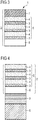
- the thin-layer encapsulation 1 according to the exemplary embodiment of FIG. 1 comprises a layer sequence 2 having a first ALD layer 3 deposited by atomic layer deposition and a second ALD layer 4 also deposited by atomic layer deposition.
- the first ALD layer 3 and the second ALD layer 4 are in particular in direct contact with each other.
- the first ALD layer 3 comprises or consists of, for example, aluminum oxide, while the second ALD layer 4 consists of zinc oxide or comprises zinc oxide. Since the two ALD layers 3, 4 presently consist of two different materials, their transmission to visible light is increased because interference effects that can reduce the transmission in a single ALD layer are at least reduced. Furthermore, the use of two different materials for the first ALD layer 3 and the second ALD layer 4 has the advantage that small diffusion channels in the ALD layers 3, 4 can be better closed.
- suitable materials for the ALD layers 3, 4 are, for example, zirconium oxide, titanium oxide, hafnium oxide and lanthanum oxide.
- the thickness of the first ALD layer 3 is according to the embodiment FIG. 1 at about 10 nm, while the second ALD layer 4 has a thickness of about 1 nm.
- the two ALD layers 3, 4 according to the embodiment of the FIG. 1 form a nanolaminate 5.
- a nanolaminate 5 alone may be capable of providing a sufficient barrier to atmospheric influences such as moisture or oxygen.
- a thin-layer encapsulation 1 according to the present application may furthermore be formed by a nanolaminate 5, in which the ALD layers 3, 4 repeat periodically.
- the thin-layer encapsulation 1 according to the exemplary embodiment of FIG. 2A has, for example, a nanolaminate 5, in which the ALD layers 3, 4 of the nanolaminate according to FIG. 1 repeat periodically three times.
- the ALD layers 3, 4 are each arranged in direct contact with each other, that is, they each form a common interface.
- the ALD layers 3, 4 of the nanolaminate 5 repeat FIG. 1 at least five times. This is not shown for reasons of clarity.
- the layer sequence 2 of the thin-film encapsulation 1 according to FIG. 2A in addition to another layer 6, which is not applied by atomic layer deposition, but for example by thermal Vaporizing or plasma enhanced methods such as sputtering or PECVD.
- the further layer 6 is in this case arranged in direct contact with the outermost first ALD layer 3 of the nanolaminate 5.
- the further layer 6 comprises silicon nitride or consists of silicon nitride and has a thickness of, for example, approximately 90 nm.
- silicon oxide silicon oxide, silicon oxynitride, indium tin oxide, indium zinc oxide, aluminum-doped zinc oxide, aluminum oxide and their mixtures and alloys are suitable for the further layer 6.
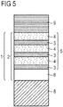
- the thin-layer encapsulation 1 according to the exemplary embodiment of FIG. 2B has a first ALD layer 3, which as in the embodiment according to FIG. 2A Has alumina or consists of alumina. Furthermore, the thin-layer encapsulation 1 has a second ALD layer 4 which comprises titanium oxide or consists of titanium oxide.
- the first ALD layer 3 is applied in direct contact with the second ALD layer 4.
- the nanolaminate 5 according to the embodiment of the FIG. 2B is formed by a threefold periodic repetition of a first ALD layer 3 comprising alumina or consisting of alumina and a second ald layer 4 comprising titania or consisting of titania. Furthermore, it is also possible that the nanolaminate 5 is formed by a quadruple or about five times periodic repetition of such first and second ALD layers 3, 4.
- the thickness of the first ALD layer 3 and the second ALD layer 4 is preferably between one atomic layer and 10 nm.
- the thickness of the first ALD layer 3, which comprises aluminum oxide or consists of aluminum oxide is about 2 nm
- Thickness of the second ALD layer 4, which comprises titanium oxide or consists of titanium oxide, is for example between approximately 7 nm and approximately 9 nm, the limits being included.
- the layer sequence 2 of the thin-layer encapsulation 1 it is also possible for the layer sequence 2 of the thin-layer encapsulation 1 to have a further ALD layer 6 'which likewise comprises titanium oxide or consists of titanium oxide and which forms the outer surface of the thin-layer encapsulation 1.
- Such a further ALD layer 6 ', which comprises titanium oxide or consists of titanium oxide has, for example, a thickness of approximately 8 nm.
- the thin-layer encapsulation 1 according to the exemplary embodiment of FIG. 3 differs from the thin-layer encapsulation 1 according to the FIG. 2A in that its layer sequence 2 comprises a second further layer 7.
- the second further layer 7 is applied to the side of the nanolaminate 5 facing away from the first further layer 6 in direct contact therewith.
- the second further layer 7 may comprise the same material as the first further layer 6 or also another material.
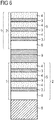
- the optoelectronic component according to the embodiment of the FIG. 4 has a substrate 8, to which an active zone 9 is applied.
- the active zone 9 is in the present case suitable for receiving or emitting radiation.
- the active zone 9 of the device comprises, for example, an organic functional material.
- the active zone 9 may also comprise an inorganic active material.
- the optoelectronic component can be, for example, an organic light-emitting diode, an organic photovoltaic cell or a solar cell. Furthermore, the optoelectronic component can also comprise organic electronics, such as transistors, diodes or organic integrated circuits.
- a thin-film encapsulation 1 On the active zone 9 of the optoelectronic component is a thin-film encapsulation 1 according to the embodiment of FIG. 2A applied.
- the thin-film encapsulation 1 is applied to the active zone 9 in such a way that the further layer 6 faces the active zone 9 and the radiation generated or received in the active zone 9 passes through the thin-layer encapsulation 1.
- the optoelectronic device according to FIG. 4 could the optoelectronic device according to FIG. 4 also a thin-layer encapsulation 1 according to the embodiments of the FIGS. 1, 2B and 3 include.
- the optoelectronic component according to the embodiment of FIG. 5 has the optoelectronic component according to the embodiment of FIG. 5 a thin-film encapsulation 1, which is arranged between the substrate 8 and the active zone 9 of the component.
- the further layer 6 of the thin-layer encapsulation 1 faces the substrate 8.
- the active zone 9 is applied to the nanolaminate 5.
- the optoelectronic component according to the embodiment of the FIG. 6 has two thin-film encapsulations 1.
- the two Dünntikverkapselitch 1 are presently identical according to the embodiment of FIG. 2A educated. But they can also be designed differently from each other.
- the first thin-layer encapsulation 1 is as in the device according to the FIG. 5 between the substrate 8 and the active region 9, while the second thin-layer encapsulation 1 is arranged above the active region 9, as in the embodiment of FIGS FIG. 4 ,
Abstract
Description
Diese Patentanmeldung beansprucht die Priorität der deutschen Patentanmeldungen
Die vorliegende Anmeldung betrifft eine Dünnschichtverkapselung für ein optoelektronisches Bauelement, ein Verfahren zu dessen Herstellung und ein optoelektronisches Bauelement.The present application relates to a thin-film encapsulation for an optoelectronic component, a method for its production and an optoelectronic component.
Optoelektronische Bauelemente und insbesondere solche, die ein organisches funktionelles Material aufweisen, wie beispielsweise organische Leuchtdioden (OLEDs), sind außerordentlich empfindlich gegenüber Feuchtigkeit und Sauerstoff. Zum Schutz vor Feuchtigkeit und Sauerstoff werden OLEDs beispielsweise in der Regel aufwändig mit Glaskavitäten verkapselt, die auf das Bauteil geklebt werden.Opto-electronic devices, and especially those having an organic functional material, such as organic light-emitting diodes (OLEDs), are extremely sensitive to moisture and oxygen. For example, to protect against moisture and oxygen, OLEDs are usually encapsulated in a costly manner with glass cavities which are glued onto the component.
Weiterhin sind Dünnschichtverkapselungen mit dünnen Schichten bekannt, die das Bauelement gegen Feuchtigkeit und Sauerstoff abdichten. Eine solche Dünnschichtverkapselung ist beispielsweise in den Anmeldungen
Aufgabe der vorliegenden Erfindung ist es, eine verbesserte Dünnschichtverkapselung für ein optoelektronisches Bauelement anzugeben. Insbesondere soll die Dünnschichtverkapselung eine gute optische Transmission für sichtbares Licht aufweisen. Weiterhin ist es Aufgabe der vorliegenden Anmeldung, ein Verfahren zur Herstellung der Dünnschichtverkapselung und ein optoelektronisches Bauelement mit einer solchen Dünnschichtverkapselung anzugeben.The object of the present invention is to specify an improved thin-film encapsulation for an optoelectronic component. In particular, the thin-layer encapsulation should have a good optical transmission for visible light. It is another object of the present application to provide a method for producing the thin-layer encapsulation and an optoelectronic component with such a thin-layer encapsulation.
Diese Aufgaben werden durch eine Dünnschichtverkapselung mit den Merkmalen des Patentanspruches 1, ein optoelektronisches Bauelement mit den Merkmalen des Patentanspruches 11, sowie durch ein Verfahren gemäß Patentanspruch 15 gelöst.These objects are achieved by a thin-layer encapsulation having the features of
Vorteilhafte Ausführungsformen sowie Weiterbildungen der vorliegenden Erfindung sind in den jeweils abhängigen Ansprüchen angegeben.Advantageous embodiments and further developments of the present invention are specified in the respective dependent claims.
Unter "Dünnschichtverkapselung" wird vorliegend eine Vorrichtung verstanden, die dazu geeignet ist, eine Barriere gegenüber atmosphärischen Stoffen, insbesondere gegenüber Feuchtigkeit und Sauerstoff, zu bilden. Mit anderen Worten ist die Dünnschichtverkapselung derart ausgebildet, dass sie von atmosphärischen Stoffen, wie Wasser oder Sauerstoff, höchstens zu sehr geringen Anteilen durchdrungen werden kann. Diese Barrierewirkung wird bei der Dünnschichtverkapselung im Wesentlichen durch dünne Schichten erzeugt, die Teil der Dünnschichtverkapselung sind. Die Schichten der Dünnschichtverkapselung weisen in der Regel eine Dicke kleiner oder gleich einiger 100 nm auf."Thin-layer encapsulation" is understood here to mean a device which is suitable for forming a barrier to atmospheric substances, in particular to moisture and oxygen. In other words, the thin-layer encapsulation is designed so that it can be penetrated by atmospheric substances such as water or oxygen, at most at very low levels. In the case of thin-layer encapsulation, this barrier effect is essentially produced by thin layers which form part of the thin-layer encapsulation. The layers of the thin-layer encapsulation generally have a thickness of less than or equal to a few 100 nm.
Gemäß einer Ausführungsform besteht die Dünnschichtverkapselung aus den dünnen Schichten, die für die Barrierewirkung der Dünnschichtverkapselung verantwortlich sind.According to one embodiment, the thin-layer encapsulation consists of the thin layers suitable for the Barrier effect of the Dünnschichtverkapselung are responsible.
Eine Dünnschichtverkapselung für ein optoelektronisches Bauelement mit einer guten Transmission für sichtbares Licht weist insbesondere eine Schichtenfolge mit folgenden Schichten auf:
- eine erste ALD-Schicht, die mittels Atomlagenabscheidung abgeschieden wurde, und
- eine zweite ALD-Schicht, die ebenfalls mittels Atomlagenabscheidung abgeschieden wurde.
- a first ALD layer deposited by atomic layer deposition, and
- a second ALD layer also deposited by atomic layer deposition.
Es sei an dieser Stelle darauf hingewiesen, dass die Schichtenfolge nicht auf zwei ALD-Schichten beschränkt ist. Vielmehr kann die Schichtenfolge weitere ALD-Schichten aufweisen. Ebenso kann die Schichtenfolge weitere Schichten aufweisen, die mittels anderer Verfahren als Atomlagenabscheidung erzeugt wurden.It should be noted at this point that the layer sequence is not limited to two ALD layers. Rather, the layer sequence can have further ALD layers. Likewise, the layer sequence can have further layers, which were produced by methods other than atomic layer deposition.
Eine Schichtenfolge, die nur ALD-Schichten aufweist, wird vorliegend auch als "Nanolaminat" bezeichnet.A layer sequence which has only ALD layers is also referred to herein as "nanolaminate".
Mit "Atomlagenabscheidung" ("atomic layer deposition", ALD) ist vorliegend ein Verfahren bezeichnet, bei dem eine erste gasförmige Ausgangsverbindung einem Volumen zugeführt wird, in dem eine zu beschichtende Oberfläche bereitgestellt ist, so dass die erste gasförmige Verbindung auf der Oberfläche adsorbieren kann. Nach einer bevorzugt vollständigen oder nahezu vollständigen Bedeckung der Oberfläche mit der ersten Ausgangsverbindung wird der Teil der ersten Ausgangsverbindung, der noch gasförmig und/oder nicht auf der Oberfläche adsorbiert vorliegt, in der Regel wieder aus dem Volumen entfernt und eine zweite Ausgangsverbindung zugeführt. Die zweite Ausgangsverbindung ist dafür vorgesehen, mit der an der Oberfläche adsorbierten, ersten Ausgangsverbindung unter Bildung einer festen ALD-Schicht chemisch zu reagieren.By "atomic layer deposition" (ALD) herein is meant a process in which a first gaseous starting compound is supplied to a volume in which a surface to be coated is provided so that the first gaseous compound can adsorb on the surface , After a preferably complete or almost complete covering of the surface with the first starting compound, the part of the first starting compound which is still present in gaseous form and / or not adsorbed on the surface is usually removed again from the volume and a second starting compound fed. The second starting compound is intended to chemically react with the first starting compound adsorbed on the surface to form a solid ALD layer.
Es sei an dieser Stelle darauf hingewiesen, dass bei der Atomlagenabscheidung auch mehr als zwei Ausgangsverbindungen zum Einsatz kommen können.It should be noted at this point that in the atomic layer deposition more than two starting compounds can be used.
Bei der Atomlagenabscheidung ist es in der Regel vorteilhaft, wenn die zu beschichtende Oberfläche auf eine Temperatur über Raumtemperatur erhitzt wird. Dadurch kann die Reaktion zur Bildung der festen ALD-Schicht thermisch initiiert werden. Die Temperatur der zu beschichteten Oberfläche ist hierbei in der Regel von den Ausgangsverbindungen abhängig.In the atomic layer deposition, it is generally advantageous if the surface to be coated is heated to a temperature above room temperature. Thereby, the reaction for forming the solid ALD layer can be thermally initiated. The temperature of the surface to be coated is usually dependent on the starting compounds.
Eine plasmalose Atomlagenabscheidung ("plasma-less atomic layer deposition", PLALD) bezeichnet vorliegend ein ALD-Verfahren, für das kein Plasma wie im Folgenden beschrieben, erzeugt wird, sondern bei dem zur Bildung der festen Schicht, die Reaktion der Ausgangsverbindungen nur über die Temperatur der zu beschichtenden Oberfläche initiiert wird.A plasma-less atomic layer deposition (PLALD) designates in the present case an ALD process for which no plasma is produced as described below, but in which the reaction of the starting compounds takes place only via the plasma phase to form the solid layer Temperature of the surface to be coated is initiated.
Die Temperatur der zu beschichtenden Oberfläche liegt bei einem PLALD-Verfahren in der Regel zwischen 60°C und 120°C, wobei die Grenzen eingeschlossen sind.The temperature of the surface to be coated is usually between 60 ° C and 120 ° C in a PLALD process, the limits being included.
Eine plasmaunterstützte Atomlagenabscheidung ("plasma enhanced atomic layer deposition", PEALD) bezeichnet vorliegend weiterhin ein ALD-Verfahren, bei dem die zweite Ausgangsverbindung bei gleichzeitiger Erzeugung eines Plasmas zugeführt wird, wodurch die zweite Ausgangsverbindung angeregt werden soll. Dadurch kann - im Vergleich zu einem plasmalosen ALD-Verfahren - die Temperatur, auf die die zu beschichtende Oberfläche aufgeheizt werden muss, verringert werden und durch die Plasmaerzeugung dennoch die Reaktion zwischen den Ausgangsverbindungen initiiert werden. Bevorzugt ist die Temperatur der zu beschichteten Oberfläche bei PEALD kleiner oder gleich 120°C, besonders bevorzugt kleiner oder gleich 80°C.Plasma-enhanced atomic layer deposition (PEALD) in the present case also refers to an ALD process in which the second starting compound is supplied with the simultaneous production of a plasma, whereby the second starting compound is to be excited. This can - compared to a non-plasmal ALD processes - the temperature at which the surface to be coated must be heated is reduced, and the plasma generation nevertheless initiates the reaction between the starting compounds. The temperature of the surface to be coated is preferably less than or equal to 120 ° C., particularly preferably less than or equal to 80 ° C., for PEALD.
Insbesondere kann ein PEALD-Verfahren vorteilhaft sein, wenn eine Initiierung der Reaktion zwischen den Ausgangsverbindungen eine Oberflächentemperatur erforderlich macht, bei der das zu verkapselnde Bauelement geschädigt werden könnte.In particular, a PEALD process may be advantageous if initiation of the reaction between the starting compounds requires a surface temperature at which the device to be encapsulated might be damaged.
Bei der Dünnschichtverkapselung befindet sich die erste ALD-Schicht besonders bevorzugt in direktem Kontakt mit der zweiten ALD-Schicht. Dies bedeutet, dass die erste ALD-Schicht und die zweite ALD-Schicht eine gemeinsame Grenzfläche aufweisen.In the case of thin-layer encapsulation, the first ALD layer is particularly preferably in direct contact with the second ALD layer. This means that the first ALD layer and the second ALD layer have a common interface.
Weiterhin ist die erste ALD-Schicht besonders bevorzugt von der zweiten ALD-Schicht bezüglich des Materials verschieden. Auf diese Art und Weise ist es möglich, die optischen Eigenschaften der Dünnschichtverkapselung derart anzupassen, dass deren Transmission für sichtbares Licht erhöht wird.Furthermore, the first ALD layer is particularly preferably different from the second ALD layer with respect to the material. In this way it is possible to adapt the optical properties of the thin-layer encapsulation in such a way that its transmission for visible light is increased.
Geeignete Materialien für die erste und/oder die zweite ALD-Schicht sind: Aluminiumoxid, Zinkoxid, Zirkoniumoxid, Titanoxid, Hafniumoxid, Lanthaniumoxid.Suitable materials for the first and / or the second ALD layer are: alumina, zinc oxide, zirconia, titania, hafnia, lanthania.
Bevorzugt sind die ALD-Schichten der Schichtenfolge besonders dünn ausgebildet, beispielsweise weisen diese eine Dicke zwischen einer Atomlage und 10 nm auf, wobei die Grenzen eingeschlossen sind. Dies trägt in der Regel zu einer hohen optischen Transmission der Dünnschichtverkapselung bei.Preferably, the ALD layers of the layer sequence are formed particularly thin, for example, they have a thickness between an atomic layer and 10 nm, wherein the limits are included. This usually contributes to a high optical transmission of the thin-layer encapsulation.
Besonders bevorzugt weist eine Dünnschichtverkapselung ein Nanolaminat auf, bei dem die erste ALD-Schicht Aluminiumoxid aufweist oder aus Aluminiumoxid besteht und die zweite ALD-Schicht Zinkoxid aufweist oder aus Zinkoxid besteht, wobei die erste ALD-Schicht und die zweite ALD-Schicht in direktem Kontakt miteinander stehen. Ein derartiges Nanolaminat weist insbesondere eine besonders hohe optische Transmission für sichtbares Licht auf, bei gleichzeitig guter Barrierewirkung.Particularly preferably, a thin-layer encapsulation comprises a nanolaminate in which the first ALD layer comprises aluminum oxide or consists of aluminum oxide and the second ALD layer comprises zinc oxide or consists of zinc oxide, the first ALD layer and the second ALD layer in direct contact standing together. Such a nanolaminate has, in particular, a particularly high optical transmission for visible light, with a simultaneously good barrier effect.
Bei einer weiteren besonders bevorzugten Ausführungsform weist eine Dünnschichtverkapselung ein Nanolaminat auf, bei dem die erste ALD-Schicht Aluminiumoxid aufweist oder aus Aluminiumoxid besteht und die zweite ALD-Schicht Titanoxid aufweist oder aus Titanoxid besteht, wobei die erste ALD-Schicht und die zweite ALD-Schicht besonders bevorzugt in direktem Kontakt miteinander stehen. Besonders bevorzugt schließt das Nanolaminat mit einer ALD-Schicht ab, die Titanoxid aufweist oder aus Titanoxid besteht, dass heißt, dass eine Außenfläche der Dünnschichtverkapselung durch eine ALD-Schicht, die Titanoxid aufweist oder aus Titanoxid besteht, gebildet ist. Auch ein derartiges Nanolaminat weist insbesondere eine besonders hohe optische Transmission für sichtbares Licht auf, bei gleichzeitig guter Barrierewirkung.In a further particularly preferred embodiment, a thin-layer encapsulation comprises a nanolaminate in which the first ALD layer comprises aluminum oxide or consists of aluminum oxide and the second ALD layer comprises titanium oxide or consists of titanium oxide, the first ALD layer and the second ALD layer Layer particularly preferably in direct contact with each other. More preferably, the nanolaminate concludes with an ALD layer comprising or consisting of titanium oxide, that is, an outer surface of the thin film encapsulant is formed by an ALD layer comprising titanium oxide or titanium oxide. Such a nanolaminate in particular also has a particularly high optical transmission for visible light, while at the same time having good barrier effect.
Gemäß einer weiteren Ausführungsform umfasst die Schichtenfolge der Dünnschichtverkapselung zumindest eine weitere Schicht, die durch thermisches Aufdampfen oder mittels eines plasmagestützten Prozesses, wie Sputtern oder Plasma-Enhanced Chemical Vapour Deposition (PECVD) abgeschieden wurde.According to a further embodiment, the layer sequence of the thin-layer encapsulation comprises at least one further layer which has been deposited by thermal vapor deposition or by means of a plasma-assisted process, such as sputtering or plasma-enhanced chemical vapor deposition (PECVD).
Geeignete Materialien für die weitere Schicht sind: Siliziumnitrid, Siliziumoxid, Siliziumoxinitrid, Indiumzinnoxid, Indiumzinkoxid, Aluminium-dotiertes Zinkoxid, Aluminiumoxid sowie deren Mischungen und Legierungen.Suitable materials for the further layer are: silicon nitride, silicon oxide, silicon oxynitride, indium tin oxide, indium zinc oxide, aluminum-doped zinc oxide, aluminum oxide and mixtures and alloys thereof.
Die weitere Schicht weist beispielsweise eine Dicke zwischen 1 nm und 5 µm auf, wobei die Grenzen eingeschlossen sind. Besonders bevorzugt weist die weitere Schicht eine Dicke zwischen 1 nm und 400 nm auf, wobei wiederum die Grenzen eingeschlossen sind.The further layer has, for example, a thickness of between 1 nm and 5 μm, the limits being included. Particularly preferably, the further layer has a thickness between 1 nm and 400 nm, again including the boundaries.
Gemäß einer besonders bevorzugten Ausführungsform ist die weitere Schicht an einer Außenseite der Schichtenfolge angeordnet.According to a particularly preferred embodiment, the further layer is arranged on an outer side of the layer sequence.
Gemäß einer bevorzugten Ausführungsform der Dünnschichtverkapselung weist diese ein Nanolaminat auf, an das in direktem Kontakt eine weitere Schicht angeordnet ist.According to a preferred embodiment of the thin-layer encapsulation, this has a nanolaminate, to which a further layer is arranged in direct contact.
Eine besonders bevorzugte Dünnschichtverkapselung, die eine hohe optische Transmission für sichtbares Licht sowie eine besonders gute hermetische Barrierewirkung gewährleistet, weist eine weitere Schicht auf, die mittels eines plasmagestützten Prozesses aufgebracht ist und Siliziumnitrid umfasst oder aus Siliziumnitrid besteht.A particularly preferred thin-layer encapsulation, which ensures high optical transmission for visible light and a particularly good hermetic barrier effect, has a further layer, which is applied by means of a plasma-supported process and comprises silicon nitride or consists of silicon nitride.
Zusätzlich oder alternativ ist es auch möglich, dass die Schichtenfolge der Dünnschichtverkapselung eine weitere ALD-Schicht aufweist. Diese weitere ALD-Schicht kann beispielsweise eines der folgenden Materialien aufweisen oder aus zumindest einem dieser Materialien bestehen: Aluminiumoxid, Zinkoxid, Zirkoniumoxid, Titanoxid, Hafniumoxid, Lanthaniumoxid. Besonders bevorzugt weist die weitere ALD-Schicht Titanoxid auf oder besteht aus diesem Material. Weiterhin bildet die weitere ALD-Schicht besonders bevorzugt eine Außenfläche der Dünnschichtverkapselung aus.Additionally or alternatively, it is also possible for the layer sequence of the thin-layer encapsulation to have a further ALD layer. This further ALD layer may, for example, comprise or consist of at least one of the following materials: aluminum oxide, zinc oxide, zirconium oxide, titanium oxide, Hafnium oxide, lanthanum oxide. Particularly preferably, the further ALD layer comprises titanium oxide or consists of this material. Furthermore, the further ALD layer particularly preferably forms an outer surface of the thin-layer encapsulation.
Gemäß einer weiteren Ausführungsform der Dünnschichtverkapselung wiederholen sich die Schichten der Schichtenfolge mehrfach, bevorzugt periodisch. Besonders bevorzugt weist die Dünnschichtverkapselung ein Nanolaminat auf, dessen ALD-Schichten sich innerhalb des Nanolaminates mehrfach oder periodisch wiederholen. Hierdurch kann vorteilhafterweise eine besonders dichte Dünnschichtverkapselung erzielt werden.According to a further embodiment of the thin-layer encapsulation, the layers of the layer sequence are repeated several times, preferably periodically. The thin-layer encapsulation particularly preferably has a nanolaminate whose ALD layers repeat multiply or periodically within the nanolaminate. As a result, advantageously a particularly dense thin-layer encapsulation can be achieved.
Bei der vorliegenden Dünnschichtverkapselung ist es vorteilhafterweise möglich, durch geeignete Auswahl der einzelnen Schichten, insbesondere hinsichtlich Dicke und Materialien der Schichten, die optischen Eigenschaften der Dünnschichtverkapselung auf gewünschte Art und Weise anzupassen. So kann beispielsweise durch eine geeignete Auswahl von Schichtdicken und Materialien der Schichten der Transmissionsgrad und die Reflektivität der Dünnschichtverkapselung auf gewünschte Art und Weise angepasst werden. Vorteilhafterweise kann etwa eine Dünnschichtverkapselung mit Entspiegelungswirkung oder mit einem gewünschten Transmissionsgrad erzielt werden.In the case of the present thin-layer encapsulation, it is advantageously possible to adapt the optical properties of the thin-layer encapsulation in a desired manner by suitably selecting the individual layers, in particular with regard to the thickness and materials of the layers. For example, by a suitable selection of layer thicknesses and materials of the layers, the transmittance and the reflectivity of the thin-layer encapsulation can be adapted in a desired manner. Advantageously, for example, a thin-layer encapsulation with an antireflection effect or with a desired degree of transmission can be achieved.
Die Dünnschichtverkapselung weist besonders bevorzugt eine Transmission für sichtbares Licht auf, die größer oder gleich 70% ist. Besonders bevorzugt ist die Transmission der Dünnschichtverkapselung für sichtbares Licht größer oder gleich 90 %.The thin-layer encapsulation particularly preferably has a transmission for visible light which is greater than or equal to 70%. Particularly preferably, the transmission of the thin-layer encapsulation for visible light is greater than or equal to 90%.
Die vorliegende Dünnschichtverkapselung ist insbesondere für optoelektronische Bauelemente geeignet, da ihre optischen Eigenschaften auf gewünschte Art und Weise angepasst werden kann.The present thin-layer encapsulation is particularly suitable for optoelectronic components, since their optical properties can be adapted in the desired manner.
Ein optoelektronisches Bauelement umfasst insbesondere:
- ein Substrat,
- eine aktive, strahlungserzeugende und/oder strahlungsempfangende Zone, die auf dem Substrat aufgebracht ist, und
- eine Dünnschichtverkapselung, wie sie oben beschrieben wurde.
- a substrate,
- an active, radiation-generating and / or radiation-receiving zone, which is applied to the substrate, and
- a thin film encapsulation as described above.
Die Dünnschichtverkapselung ist bevorzugt zwischen der aktiven Zone und dem Substrat aufgebracht. Diese Anordnung schützt vorteilhafterweise insbesondere die empfindliche aktive Zone.The thin-layer encapsulation is preferably applied between the active zone and the substrate. This arrangement advantageously protects in particular the sensitive active zone.
Zur Herstellung einer solchen Anordnung wird in der Regel erst die Dünnschichtverkapselung auf das Substrat aufgebracht und anschließend die aktive Zone über der Dünnschichtverkapselung.In order to produce such an arrangement, the thin-layer encapsulation is usually first applied to the substrate and then the active zone above the thin-layer encapsulation.
Die vorliegende Dünnschichtverkapselung ist insbesondere geeignet, auf flexible Substrate, wie beispielsweise Metallfolien oder Kunststofffolien aufgebracht zu werden, da diese aufgrund der geringen Dicke der Dünnschichtverkapselung ihre Flexibilität durch die Dünnschichtverkapselung nicht verlieren.The present thin-layer encapsulation is particularly suitable for being applied to flexible substrates, such as metal foils or plastic films, since they do not lose their flexibility due to the thin-layer encapsulation due to the small thickness of the thin-layer encapsulation.
Gemäß einer weiteren bevorzugten Ausführungsform ist die Dünnschichtverkapselung derart über der aktiven Zone angebracht, dass die in der aktiven Zone erzeugte oder empfangene Strahlung durch die Dünnschichtverkapselung hindurch läuft.According to a further preferred embodiment, the thin-layer encapsulation is so mounted over the active zone that the generated in the active zone or received radiation passes through the thin-film encapsulation.
Die vorliegende Dünnschichtverkapselung ist insbesondere geeignet, bei einer organischen Leuchtdiode, einer organischen Fotovoltaikzelle, einer Solarzelle angewendet zu werden oder bei einem optoelektronischen Bauelement, das eine organische Elektronik - wie z.B. Transistoren, Dioden oder organische integrierte Schaltkreise - aufweist.The present thin-layer encapsulation is particularly suitable for use in an organic light-emitting diode, an organic photovoltaic cell, a solar cell or in an optoelectronic component which has an organic electronic device - such as e.g. Transistors, diodes or organic integrated circuits - has.
Bei dem Verfahren zur Herstellung einer Dünnschichtverkapselung für ein optoelektronisches Bauelement werden eine erste ALD-Schicht und eine zweite ALD-Schicht jeweils mittels Atomlagenabscheidung abgeschieden. Die zuvor im Zusammenhang mit der Dünnschichtverkapselung beschriebenen vorteilhaften Ausgestaltungen gelten analog auch für das Verfahren.In the method for producing a thin-film encapsulation for an optoelectronic component, a first ALD layer and a second ALD layer are each deposited by means of atomic layer deposition. The advantageous embodiments described above in connection with the thin-layer encapsulation apply analogously to the method as well.
Weitere vorteilhafte Ausführungsformen und Weiterbildungen der Erfindung ergeben sich aus den im Folgenden in Verbindung mit den Figuren beschriebenen Ausführungsbeispielen.Further advantageous embodiments and developments of the invention will become apparent from the embodiments described below in conjunction with the figures.
Es zeigen:
-
Figuren 1bis 3 -
Figuren 4bis 6
-
FIGS. 1 to 3 schematic sectional views each of a thin-film encapsulation according to each embodiment, and -
FIGS. 4 to 6 schematic sectional views of an optoelectronic component according to one embodiment in each case.
In den Ausführungsbeispielen und Figuren sind gleiche oder gleich wirkende Bestandteile jeweils mit den gleichen Bezugszeichen versehen. Die dargestellten Elemente und deren Größenverhältnisse untereinander sind nicht als maßstabsgerecht anzusehen, vielmehr können einzelne Elemente, insbesondere Schichtdicken, zum besseren Verständnis übertrieben groß dargestellt sein.In the exemplary embodiments and figures, identical or identically acting components are each provided with the same reference numerals. The illustrated elements and their proportions with each other are not to be regarded as true to scale, but individual elements, in particular layer thicknesses, for exaggerated understanding be shown exaggerated.
Die Dünnschichtverkapselung 1 gemäß dem Ausführungsbeispiel der
Die erste ALD-Schicht 3 umfasst oder besteht zum Beispiel aus Aluminiumoxid, während die zweite ALD-Schicht 4 aus Zinkoxid besteht oder Zinkoxid aufweist. Da die beiden ALD-Schichten 3, 4 vorliegend aus zwei verschiedenen Materialien bestehen, ist deren Transmission gegenüber sichtbarem Licht erhöht, da Interferenzeffekte, die bei einer einzigen ALD-Schicht die Transmission erniedrigen können, zumindest vermindert werden. Weiterhin hat die Verwendung zweier verschiedener Materialien für die erste ALD-Schicht 3 und die zweite ALD-Schicht 4 den Vorteil, dass kleine Diffusionskanäle in den ALD-Schichten 3, 4 besser geschlossen werden können.The
Weitere geeignete Materialien für die ALD-Schichten 3, 4 sind beispielsweise Zirkoniumoxid, Titanoxid, Hafniumoxid und Lanthaniumoxid.Other suitable materials for the ALD layers 3, 4 are, for example, zirconium oxide, titanium oxide, hafnium oxide and lanthanum oxide.
Die Dicke der ersten ALD-Schicht 3 liegt bei dem Ausführungsbeispiel gemäß
Die beiden ALD-Schichten 3, 4 gemäß dem Ausführungsbeispiel der
Eine Dünnschichtverkapselung 1 gemäß der vorliegenden Anmeldung kann weiterhin durch ein Nanolaminat 5 gebildet sein, bei dem sich die ALD-Schichten 3, 4 periodisch wiederholen.A thin-
Die Dünnschichtverkapselung 1 gemäß dem Ausführungsbeispiel der
Die ALD-Schichten 3, 4 sind herbei jeweils in direktem Kontakt miteinander angeordnet, dass heißt, sie bilden jeweils eine gemeinsame Grenzfläche aus.The ALD layers 3, 4 are each arranged in direct contact with each other, that is, they each form a common interface.
Bei einer besonders bevorzugten Ausführungsform wiederholen sich die ALD-Schichten 3, 4 des Nanolaminats 5 der
Neben dem Nanolaminat 5 weist die Schichtenfolge 2 der Dünnschichtverkapselung 1 gemäß
Die weitere Schicht 6 ist hierbei in direktem Kontakt mit der äußersten ersten ALD-Schicht 3 des Nanolaminats 5 angeordnet.The
Bei dem Ausführungsbeispiel der
Für die weitere Schicht 6 sind neben Siliziumnitrid die Materialien Siliziumoxid, Siliziumoxinitrid, Indiumzinnoxid, Indiumzinkoxid, Aluminium-dotiertes Zinkoxid Aluminiumoxid sowie deren Mischungen und Legierungen geeignet.In addition to silicon nitride, the materials silicon oxide, silicon oxynitride, indium tin oxide, indium zinc oxide, aluminum-doped zinc oxide, aluminum oxide and their mixtures and alloys are suitable for the
Die Dünnschichtverkapselung 1 gemäß dem Ausführungsbeispiel der
Die Dicke der ersten ALD-Schicht 3 und der zweiten ALD-Schicht 4, liegt bevorzugt zwischen einer Atomlage und 10 nm. Beispielsweise beträgt die Dicke der ersten ALD-Schicht 3, die Aluminiumoxid aufweist oder aus Aluminiumoxid besteht, ca. 2 nm. Die Dicke der zweiten ALD-Schicht 4, die Titanoxid aufweist oder aus Titanoxid besteht, liegt beispielsweise zwischen ca. 7 nm und ca. 9 nm, wobei die Grenzen eingeschlossen sind.The thickness of the
Besonders bevorzugt ist die Dünnschichtverkapselung gemäß dem Ausführungsbeispiel der
Die Dünnschichtverkapselung 1 gemäß dem Ausführungsbeispiel der
Das optoelektronische Bauelement gemäß dem Ausführungsbeispiel der
Die aktive Zone 9 des Bauelementes umfasst beispielsweise ein organisches funktionelles Material. Alternativ kann die aktive Zone 9 auch ein anorganisches aktives Material aufweisen.The
Bei dem optoelektronischen Bauelement kann es sich beispielsweise um eine organische Leuchtdiode, eine organische Fotovoltaikzelle oder eine Solarzelle handeln. Weiterhin kann das optoelektronische Bauelement auch eine organische Elektronik - wie etwa Transistoren, Dioden oder organische integrierte Schaltkreise umfassen.The optoelectronic component can be, for example, an organic light-emitting diode, an organic photovoltaic cell or a solar cell. Furthermore, the optoelectronic component can also comprise organic electronics, such as transistors, diodes or organic integrated circuits.
Auf die aktive Zone 9 des optoelektronischen Bauelementes ist eine Dünnschichtverkapselung 1 gemäß dem Ausführungsbeispiel der
Anstelle der Dünnschichtverkapselung 1 gemäß dem Ausführungsbeispiel der
Im Unterschied zu dem Ausführungsbeispiel gemäß der
Die erste Dünnschichtverkapselung 1 ist wie bei dem Bauelement gemäß der
Die Erfindung ist nicht durch die Beschreibung anhand der Ausführungsbeispiele auf diese beschränkt. Vielmehr umfasst die Erfindung jedes neue Merkmal sowie jede Kombination von Merkmalen, was insbesondere jede Kombination von Merkmalen in den Patentansprüchen beinhaltet, auch wenn dieses Merkmal oder diese Kombination selbst nicht explizit in den Patentansprüchen oder Ausführungsbeispielen angegeben ist.The invention is not limited by the description based on the embodiments of these. Rather, the invention encompasses any novel feature as well as any combination of features, including in particular any combination of features in the claims, even if this feature or combination itself is not explicitly stated in the patent claims or exemplary embodiments.
Claims (15)
Applications Claiming Priority (3)
| Application Number | Priority Date | Filing Date | Title |
|---|---|---|---|
| DE102009014543 | 2009-03-24 | ||
| DE102009024411A DE102009024411A1 (en) | 2009-03-24 | 2009-06-09 | Thin-film encapsulation for an optoelectronic component, method for its production and optoelectronic component |
| EP10710030.7A EP2412040B1 (en) | 2009-03-24 | 2010-03-22 | Thin-layer encapsulation for an optoelectronic component, method for the production thereof, and optoelectronic component |
Related Parent Applications (2)
| Application Number | Title | Priority Date | Filing Date |
|---|---|---|---|
| EP10710030.7 Division | 2010-03-22 | ||
| EP10710030.7A Division-Into EP2412040B1 (en) | 2009-03-24 | 2010-03-22 | Thin-layer encapsulation for an optoelectronic component, method for the production thereof, and optoelectronic component |
Publications (1)
| Publication Number | Publication Date |
|---|---|
| EP2472629A1 true EP2472629A1 (en) | 2012-07-04 |
Family
ID=42664172
Family Applications (2)
| Application Number | Title | Priority Date | Filing Date |
|---|---|---|---|
| EP10710030.7A Active EP2412040B1 (en) | 2009-03-24 | 2010-03-22 | Thin-layer encapsulation for an optoelectronic component, method for the production thereof, and optoelectronic component |
| EP12161502A Withdrawn EP2472629A1 (en) | 2009-03-24 | 2010-03-22 | Thin-layer encapsulation for an opto-electronic component, method for producing same and opto-electronic component |
Family Applications Before (1)
| Application Number | Title | Priority Date | Filing Date |
|---|---|---|---|
| EP10710030.7A Active EP2412040B1 (en) | 2009-03-24 | 2010-03-22 | Thin-layer encapsulation for an optoelectronic component, method for the production thereof, and optoelectronic component |
Country Status (7)
| Country | Link |
|---|---|
| US (1) | US9444062B2 (en) |
| EP (2) | EP2412040B1 (en) |
| JP (1) | JP6073130B2 (en) |
| KR (1) | KR101722277B1 (en) |
| CN (1) | CN102362369B (en) |
| DE (1) | DE102009024411A1 (en) |
| WO (1) | WO2010108894A1 (en) |
Families Citing this family (60)
| Publication number | Priority date | Publication date | Assignee | Title |
|---|---|---|---|---|
| DE102009024411A1 (en) | 2009-03-24 | 2010-09-30 | Osram Opto Semiconductors Gmbh | Thin-film encapsulation for an optoelectronic component, method for its production and optoelectronic component |
| FR2949775B1 (en) | 2009-09-10 | 2013-08-09 | Saint Gobain Performance Plast | PROTECTIVE SUBSTRATE FOR COLOR DEVICE OR RADIATION TRANSMITTER |
| FR2949776B1 (en) | 2009-09-10 | 2013-05-17 | Saint Gobain Performance Plast | LAYERED ELEMENT FOR ENCAPSULATING A SENSITIVE ELEMENT |
| FR2973940A1 (en) * | 2011-04-08 | 2012-10-12 | Saint Gobain | LAYERED ELEMENT FOR ENCAPSULATING A SENSITIVE ELEMENT |
| FR2973939A1 (en) | 2011-04-08 | 2012-10-12 | Saint Gobain | LAYERED ELEMENT FOR ENCAPSULATING A SENSITIVE ELEMENT |
| DE102011079004A1 (en) | 2011-07-12 | 2013-01-17 | Osram Opto Semiconductors Gmbh | ORGANIC LIGHT-EMITTING COMPONENT AND METHOD FOR PRODUCING AN ORGANIC LIGHT-EMITTING COMPONENT |
| DE102011079048A1 (en) | 2011-07-13 | 2013-01-17 | Osram Opto Semiconductors Gmbh | LIGHT-EMITTING COMPONENTS AND METHOD FOR PRODUCING A LIGHT-EMITTING COMPONENT |
| KR101658822B1 (en) | 2011-07-14 | 2016-09-22 | 오스람 오엘이디 게엠베하 | Encapsulation structure for an optoelectronic component and method for encapsulating an optoelectronic component |
| DE102011113428A1 (en) | 2011-09-14 | 2013-03-14 | Osram Opto Semiconductors Gmbh | Optoelectronic component |
| DE102011084276B4 (en) | 2011-10-11 | 2019-10-10 | Osram Oled Gmbh | Encapsulation for an organic electrical component, an organic electronic component with the encapsulation and a method for the production of an organic electronic component with the encapsulation |
| DE102012203212A1 (en) | 2012-03-01 | 2013-09-05 | Osram Opto Semiconductors Gmbh | Coating system useful for producing layer on substrate using growth process, preferably for performing atomic layer deposition, comprises supply container, in which liquid starting material for layer is provided, and evaporator unit |
| DE102012208142B4 (en) | 2012-05-15 | 2021-05-12 | Pictiva Displays International Limited | ORGANIC LIGHT EMITTING COMPONENT AND METHOD FOR MANUFACTURING AN ORGANIC LIGHT EMITTING COMPONENT |
| DE102012211869A1 (en) | 2012-07-06 | 2014-01-09 | Osram Opto Semiconductors Gmbh | Organic light emitting device |
| DE102012214216A1 (en) | 2012-08-09 | 2014-02-13 | Osram Opto Semiconductors Gmbh | Organic light-emitting diode module and method for its production |
| DE102012214325B4 (en) * | 2012-08-10 | 2017-06-08 | Osram Oled Gmbh | Method for producing an optoelectronic component and method for structuring an organic, optoelectronic component |
| KR101970361B1 (en) | 2012-08-20 | 2019-04-19 | 삼성디스플레이 주식회사 | Organic light emitting diode device and manufacturing method thereof |
| CN102864417A (en) * | 2012-08-22 | 2013-01-09 | 吉林大学 | Method for encapsulating organic devices by passivation layer prepared by electron beam evaporation and atomic layer deposition |
| DE102012215708A1 (en) | 2012-09-05 | 2014-03-06 | Osram Opto Semiconductors Gmbh | STORAGE CONTAINER FOR A COATING SYSTEM AND COATING SYSTEM |
| DE102012221080A1 (en) * | 2012-11-19 | 2014-03-06 | Osram Opto Semiconductors Gmbh | Method for producing a layer on a surface region of an electronic component |
| KR101528407B1 (en) * | 2012-11-29 | 2015-06-11 | 주식회사 엘지화학 | Coating method for decreasing damage of inorganic thin layer |
| JP6036279B2 (en) * | 2012-12-26 | 2016-11-30 | コニカミノルタ株式会社 | Organic electroluminescence device manufacturing method |
| CN104134756A (en) * | 2013-04-30 | 2014-11-05 | 成均馆大学校产学协力团 | Multilayer encapsulation thin-film |
| KR101465212B1 (en) * | 2013-04-30 | 2014-11-25 | 성균관대학교산학협력단 | Ultra-flexible encapsulation thin-film |
| DE102013105128A1 (en) | 2013-05-17 | 2014-11-20 | Osram Opto Semiconductors Gmbh | Optoelectronic component |
| KR20150018964A (en) | 2013-08-12 | 2015-02-25 | 삼성디스플레이 주식회사 | Organic light emitting display device and methode for manufacturing the same |
| DE102013108871A1 (en) | 2013-08-16 | 2015-03-12 | Osram Opto Semiconductors Gmbh | Organic light emitting device |
| DE102013109646B4 (en) | 2013-09-04 | 2021-12-02 | Pictiva Displays International Limited | Organic optoelectronic component |
| JP6672152B2 (en) * | 2013-09-30 | 2020-03-25 | エルジー・ケム・リミテッド | Substrate for organic electronic device and method for producing the same |
| KR101928598B1 (en) * | 2013-09-30 | 2018-12-12 | 주식회사 엘지화학 | Polyimide film and process for preparing same |
| FR3020179B1 (en) * | 2014-04-22 | 2017-10-06 | Saint Gobain | ELECTRODE SUPPORTED TRANSPARENT FOR OLED |
| DE102014106549B4 (en) | 2014-05-09 | 2023-10-19 | Pictiva Displays International Limited | Organic light-emitting component |
| DE102014108282A1 (en) | 2014-06-12 | 2015-12-17 | Osram Opto Semiconductors Gmbh | Optoelectronic semiconductor component, method for producing an optoelectronic semiconductor component and light source with an optoelectronic semiconductor component |
| EP2960315A1 (en) | 2014-06-27 | 2015-12-30 | cynora GmbH | Organic electroluminescent device |
| DE102014110969A1 (en) | 2014-08-01 | 2016-02-04 | Osram Oled Gmbh | Organic component and method for producing an organic component |
| DE102014118354A1 (en) | 2014-09-12 | 2016-03-17 | Osram Oled Gmbh | Organic component |
| WO2016042070A1 (en) | 2014-09-17 | 2016-03-24 | Cynora Gmbh | Organic molecules for use as emitters |
| DE102014116141B4 (en) | 2014-11-05 | 2022-07-28 | OSRAM Opto Semiconductors Gesellschaft mit beschränkter Haftung | Method for producing at least one optoelectronic semiconductor chip, optoelectronic semiconductor chip and optoelectronic semiconductor component |
| DE102014223507A1 (en) | 2014-11-18 | 2016-05-19 | Osram Oled Gmbh | Organic light emitting device and method of making an organic light emitting device |
| JP2016100315A (en) * | 2014-11-26 | 2016-05-30 | パイオニア株式会社 | Light-emitting device |
| JP2016103443A (en) * | 2014-11-28 | 2016-06-02 | パイオニア株式会社 | Light-emitting device |
| KR102382025B1 (en) * | 2015-03-04 | 2022-04-04 | 삼성디스플레이 주식회사 | Display apparatus |
| DE102015105766A1 (en) | 2015-04-15 | 2016-10-20 | Osram Oled Gmbh | Holding device for an organic light emitting diode and OLED module |
| DE102015107471A1 (en) | 2015-05-12 | 2016-11-17 | Osram Oled Gmbh | Organic light emitting device |
| CN107534095A (en) * | 2015-05-14 | 2018-01-02 | 应用材料公司 | Encapsulation membrane stack for OLED applications |
| DE102015110241A1 (en) | 2015-06-25 | 2016-12-29 | Osram Oled Gmbh | A method of controlling an organic light emitting device, a light emitting device having an organic light emitting device, and headlamps having a light emitting device |
| DE102015118417A1 (en) | 2015-10-28 | 2017-05-04 | Osram Oled Gmbh | Optoelectronic component and method for producing an optoelectronic component |
| CN105449123B (en) * | 2015-11-18 | 2018-03-06 | 上海大学 | The preparation method of water oxygen barrier layer |
| KR102228408B1 (en) * | 2016-10-06 | 2021-03-17 | 주식회사 원익아이피에스 | Method of Manufacturing Hard Mask |
| TWI661076B (en) * | 2016-10-06 | 2019-06-01 | 南韓商圓益Ips股份有限公司 | Method of manufacturing composite layer |
| KR102228412B1 (en) * | 2016-11-03 | 2021-03-17 | 주식회사 원익아이피에스 | Method of Manufacturing Hard Mask |
| KR102268492B1 (en) * | 2017-09-22 | 2021-06-25 | 주식회사 원익아이피에스 | Method of Manufacturing Composite Layer |
| WO2018156218A1 (en) * | 2016-11-07 | 2018-08-30 | The Regents Of The University Of Colorado, A Body Corporate | Improved performance of technical ceramics |
| JP6924023B2 (en) * | 2016-12-16 | 2021-08-25 | パイオニア株式会社 | Light emitting device |
| JP6815901B2 (en) * | 2017-03-06 | 2021-01-20 | 株式会社日本製鋼所 | Display device and its manufacturing method |
| CN108666438A (en) * | 2017-04-01 | 2018-10-16 | 上海和辉光电有限公司 | Display panel and display device |
| CN107819075A (en) * | 2017-11-02 | 2018-03-20 | 长沙新材料产业研究院有限公司 | A kind of method that flexible perovskite solar cell is integrated on aerostatics utricule |
| CN108598198A (en) * | 2018-04-26 | 2018-09-28 | 上海空间电源研究所 | A kind of resistance to elemental oxygen flexibility high transparency conductive packaging material |
| JP2019195001A (en) * | 2019-08-20 | 2019-11-07 | パイオニア株式会社 | Light emission device |
| JP2020053411A (en) | 2019-12-26 | 2020-04-02 | パイオニア株式会社 | Light-emitting device |
| KR20210133493A (en) | 2020-04-29 | 2021-11-08 | 삼성전자주식회사 | Sensor and electronic device |
Citations (6)
| Publication number | Priority date | Publication date | Assignee | Title |
|---|---|---|---|---|
| WO2006014591A2 (en) * | 2004-07-08 | 2006-02-09 | Itn Energy Systems, Inc. | Permeation barriers for flexible electronics |
| DE102008019900A1 (en) | 2008-01-30 | 2009-08-06 | Osram Opto Semiconductors Gmbh | Organic opto-electronic component i.e. organic LED, manufacturing method, involves applying barrier layers on organic functional layer by plasma enhanced atomic layer deposition and by plasma-enhanced chemical vapor deposition |
| WO2009094997A1 (en) * | 2008-01-30 | 2009-08-06 | Osram Opto Semiconductors Gmbh | Method for producing an electronic component and electronic component |
| DE102008031405A1 (en) | 2008-07-02 | 2010-01-07 | Osram Opto Semiconductors Gmbh | Barrier layer-encapsulated electronic component, e.g. LED, is obtained by successively applying layers by plasma-less atomic layer deposition and plasma-enhanced chemical vapor deposition |
| DE102008048472A1 (en) | 2008-09-23 | 2010-03-25 | Osram Opto Semiconductors Gmbh | Barrier layer-encapsulated electronic component, e.g. LED, is obtained by successively applying layers by plasma-less atomic layer deposition and plasma-enhanced chemical vapor deposition |
| DE102009024411A1 (en) | 2009-03-24 | 2010-09-30 | Osram Opto Semiconductors Gmbh | Thin-film encapsulation for an optoelectronic component, method for its production and optoelectronic component |
Family Cites Families (31)
| Publication number | Priority date | Publication date | Assignee | Title |
|---|---|---|---|---|
| US4507393A (en) * | 1983-08-11 | 1985-03-26 | Schott Glass Technologies, Inc. | Highly prefractive, low dispersion optical glass suitable for multifocal corrective lenses |
| PT1208244E (en) | 1999-04-03 | 2004-09-30 | Leibniz Inst Festkorper Werkst | METAL MATERIAL BASED ON NICKEL AND A METHOD FOR ITS PRODUCTION |
| US7198832B2 (en) * | 1999-10-25 | 2007-04-03 | Vitex Systems, Inc. | Method for edge sealing barrier films |
| JP4556282B2 (en) * | 2000-03-31 | 2010-10-06 | 株式会社デンソー | Organic EL device and method for manufacturing the same |
| TW548239B (en) | 2000-10-23 | 2003-08-21 | Asm Microchemistry Oy | Process for producing aluminium oxide films at low temperatures |
| JP3687582B2 (en) * | 2001-09-12 | 2005-08-24 | ウシオ電機株式会社 | Discharge lamp |
| JP3724454B2 (en) * | 2002-05-31 | 2005-12-07 | 株式会社デンソー | Thin film formation method |
| DE10307095A1 (en) * | 2003-02-19 | 2004-09-02 | Merck Patent Gmbh | Evaporation material for the production of high refractive index optical layers |
| JP4186688B2 (en) * | 2003-04-17 | 2008-11-26 | 三菱化学株式会社 | Electroluminescence element |
| US7212485B2 (en) * | 2003-04-14 | 2007-05-01 | Hoya Corporation | Objective lens and method for manufacture thereof |
| KR20060006840A (en) | 2003-05-16 | 2006-01-19 | 이 아이 듀폰 디 네모아 앤드 캄파니 | Barrier films for plastic substrates fabricated by atomic layer deposition |
| CN1657976A (en) * | 2004-02-16 | 2005-08-24 | 柯尼卡美能达精密光学株式会社 | Optical element and optical pickup apparatus |
| US20050181535A1 (en) | 2004-02-17 | 2005-08-18 | Yun Sun J. | Method of fabricating passivation layer for organic devices |
| JP4363365B2 (en) | 2004-07-20 | 2009-11-11 | 株式会社デンソー | Color organic EL display and manufacturing method thereof |
| US20060063015A1 (en) * | 2004-09-23 | 2006-03-23 | 3M Innovative Properties Company | Protected polymeric film |
| JP5464775B2 (en) | 2004-11-19 | 2014-04-09 | エイエスエム インターナショナル エヌ.ヴェー. | Method for producing metal oxide film at low temperature |
| JP5066814B2 (en) * | 2005-03-11 | 2012-11-07 | 三菱化学株式会社 | ELECTROLUMINESCENT ELEMENT AND LIGHTING DEVICE |
| US8125128B2 (en) | 2005-03-11 | 2012-02-28 | Mitsubishi Chemical Corporation | Electroluminescence element and lighting apparatus |
| JP2007052100A (en) * | 2005-08-16 | 2007-03-01 | Konica Minolta Opto Inc | Optical reflection member |
| KR100792139B1 (en) * | 2006-02-06 | 2008-01-04 | 주식회사 엘지화학 | Organic light emitting device using an inorganic insulating layer as an electron injection layer and method for fabricating the same |
| US20070295390A1 (en) * | 2006-05-05 | 2007-12-27 | Nanosolar, Inc. | Individually encapsulated solar cells and solar cell strings having a substantially inorganic protective layer |
| US20070295388A1 (en) * | 2006-05-05 | 2007-12-27 | Nanosolar, Inc. | Solar assembly with a multi-ply barrier layer and individually encapsulated solar cells or solar cell strings |
| US7781031B2 (en) * | 2006-12-06 | 2010-08-24 | General Electric Company | Barrier layer, composite article comprising the same, electroactive device, and method |
| US8174187B2 (en) * | 2007-01-15 | 2012-05-08 | Global Oled Technology Llc | Light-emitting device having improved light output |
| US8241713B2 (en) * | 2007-02-21 | 2012-08-14 | 3M Innovative Properties Company | Moisture barrier coatings for organic light emitting diode devices |
| JP2008235760A (en) * | 2007-03-23 | 2008-10-02 | Denso Corp | Method of manufacturing insulating film |
| DE102007024152A1 (en) * | 2007-04-18 | 2008-10-23 | Osram Opto Semiconductors Gmbh | Organic optoelectronic component |
| US20090079328A1 (en) * | 2007-09-26 | 2009-03-26 | Fedorovskaya Elena A | Thin film encapsulation containing zinc oxide |
| US20090081356A1 (en) * | 2007-09-26 | 2009-03-26 | Fedorovskaya Elena A | Process for forming thin film encapsulation layers |
| US20090278454A1 (en) * | 2008-05-12 | 2009-11-12 | Fedorovskaya Elena A | Oled display encapsulated with a filter |
| KR101084267B1 (en) | 2009-02-26 | 2011-11-16 | 삼성모바일디스플레이주식회사 | Organic light emitting diode display and method for manufactureing the same |
-
2009
- 2009-06-09 DE DE102009024411A patent/DE102009024411A1/en not_active Withdrawn
-
2010
- 2010-03-22 US US13/260,560 patent/US9444062B2/en active Active
- 2010-03-22 CN CN201080013287.1A patent/CN102362369B/en active Active
- 2010-03-22 EP EP10710030.7A patent/EP2412040B1/en active Active
- 2010-03-22 WO PCT/EP2010/053717 patent/WO2010108894A1/en active Application Filing
- 2010-03-22 JP JP2012501272A patent/JP6073130B2/en active Active
- 2010-03-22 EP EP12161502A patent/EP2472629A1/en not_active Withdrawn
- 2010-03-22 KR KR1020117025037A patent/KR101722277B1/en active IP Right Grant
Patent Citations (6)
| Publication number | Priority date | Publication date | Assignee | Title |
|---|---|---|---|---|
| WO2006014591A2 (en) * | 2004-07-08 | 2006-02-09 | Itn Energy Systems, Inc. | Permeation barriers for flexible electronics |
| DE102008019900A1 (en) | 2008-01-30 | 2009-08-06 | Osram Opto Semiconductors Gmbh | Organic opto-electronic component i.e. organic LED, manufacturing method, involves applying barrier layers on organic functional layer by plasma enhanced atomic layer deposition and by plasma-enhanced chemical vapor deposition |
| WO2009094997A1 (en) * | 2008-01-30 | 2009-08-06 | Osram Opto Semiconductors Gmbh | Method for producing an electronic component and electronic component |
| DE102008031405A1 (en) | 2008-07-02 | 2010-01-07 | Osram Opto Semiconductors Gmbh | Barrier layer-encapsulated electronic component, e.g. LED, is obtained by successively applying layers by plasma-less atomic layer deposition and plasma-enhanced chemical vapor deposition |
| DE102008048472A1 (en) | 2008-09-23 | 2010-03-25 | Osram Opto Semiconductors Gmbh | Barrier layer-encapsulated electronic component, e.g. LED, is obtained by successively applying layers by plasma-less atomic layer deposition and plasma-enhanced chemical vapor deposition |
| DE102009024411A1 (en) | 2009-03-24 | 2010-09-30 | Osram Opto Semiconductors Gmbh | Thin-film encapsulation for an optoelectronic component, method for its production and optoelectronic component |
Non-Patent Citations (1)
| Title |
|---|
| MEYER J ET AL: "Al2O3/ZrO2 Nanolaminates as Utrahigh Gas-Diffusion Barriers- A Strategy for Reliable Encapsulation of Organic Electronics", ADVANCED MATERIALS, WILEY VCH VERLAG, DE, vol. 21, no. 18, 19 February 2009 (2009-02-19), pages 1845 - 1849, XP002586026, ISSN: 0935-9648, DOI: 10.1002/ADMA.200803440 * |
Also Published As
| Publication number | Publication date |
|---|---|
| JP6073130B2 (en) | 2017-02-01 |
| JP2012521623A (en) | 2012-09-13 |
| CN102362369B (en) | 2016-10-26 |
| CN102362369A (en) | 2012-02-22 |
| WO2010108894A1 (en) | 2010-09-30 |
| KR20120001778A (en) | 2012-01-04 |
| EP2412040A1 (en) | 2012-02-01 |
| EP2412040B1 (en) | 2018-07-18 |
| DE102009024411A1 (en) | 2010-09-30 |
| US20120132953A1 (en) | 2012-05-31 |
| US9444062B2 (en) | 2016-09-13 |
| KR101722277B1 (en) | 2017-03-31 |
Similar Documents
| Publication | Publication Date | Title |
|---|---|---|
| EP2412040B1 (en) | Thin-layer encapsulation for an optoelectronic component, method for the production thereof, and optoelectronic component | |
| DE102014107264A1 (en) | ORGANIC LIGHT EMITTING DISPLAY APPARATUS CROPPED WITH A HYDROPHOBIC ORGANIC THIN FILM AND METHOD OF MANUFACTURING THEREOF | |
| DE102012208142B4 (en) | ORGANIC LIGHT EMITTING COMPONENT AND METHOD FOR MANUFACTURING AN ORGANIC LIGHT EMITTING COMPONENT | |
| WO2009095006A1 (en) | Device comprising an encapsulation unit | |
| EP2421707A1 (en) | Transparent barrier laminates | |
| EP2005485A2 (en) | Glassless solar power module comprising at least one flexible thin-film solar cell and method for producing the same | |
| EP2614536B1 (en) | Thin-film encapsulation, optoelectronic semiconductor body comprising a thin-film encapsulation and method for producing a thin-film encapsulation | |
| DE102004040277B4 (en) | A reflective layer system having a plurality of layers for application to a III / V compound semiconductor material | |
| WO2017178233A1 (en) | Multi-layer encapsulation, method for encapsulation and optoelectronic component | |
| DE102011005612A1 (en) | Organic optoelectronic component and method for producing an optoelectronic component | |
| DE102015105484A1 (en) | Organic light emitting device | |
| DE102010042982A1 (en) | Electronic component and method for manufacturing an electronic component | |
| DE102006024893A1 (en) | scintillator | |
| DE102011079101A1 (en) | ORGANIC OPTOELECTRONIC COMPONENT AND METHOD FOR THE PRODUCTION THEREOF | |
| EP2699705B1 (en) | Method of depositing a transparent barrier coating system | |
| DE102020200053A1 (en) | Encapsulation system for an optoelectronic component with at least one first encapsulation and one second encapsulation, optoelectronic component with such an encapsulation system | |
| WO2019145229A1 (en) | Optoelectronic component and method for producing an optoelectronic component | |
| WO2016102584A1 (en) | Optoelectronic assembly and method for producing an optoelectronic assembly | |
| DE102016100914B4 (en) | Method for producing a porous refractive index gradient layer | |
| DE102006042327B4 (en) | Apparatus and method for forming thin silicon nitride films on surfaces of crystalline silicon solar wafers | |
| DE102010006134B4 (en) | UV absorbing coating system, process for its preparation and plastic substrate | |
| WO2017029367A1 (en) | Method for producing an optoelectronic component and optoelectronic component | |
| WO2015082687A1 (en) | Optoelectronic component and method for producing an optoelectronic component | |
| DE102016100907B4 (en) | Method for producing a reflection-reducing layer system | |
| DE102016109874B4 (en) | Method for producing a radiation-emitting component and radiation-emitting component |
Legal Events
| Date | Code | Title | Description |
|---|---|---|---|
| AC | Divisional application: reference to earlier application |
Ref document number: 2412040 Country of ref document: EP Kind code of ref document: P |
|
| AK | Designated contracting states |
Kind code of ref document: A1 Designated state(s): AT BE BG CH CY CZ DE DK EE ES FI FR GB GR HR HU IE IS IT LI LT LU LV MC MK MT NL NO PL PT RO SE SI SK SM TR |
|
| PUAI | Public reference made under article 153(3) epc to a published international application that has entered the european phase |
Free format text: ORIGINAL CODE: 0009012 |
|
| 17P | Request for examination filed |
Effective date: 20121212 |
|
| RAP1 | Party data changed (applicant data changed or rights of an application transferred) |
Owner name: OSRAM OLED GMBH |
|
| 17Q | First examination report despatched |
Effective date: 20170223 |
|
| STAA | Information on the status of an ep patent application or granted ep patent |
Free format text: STATUS: THE APPLICATION IS DEEMED TO BE WITHDRAWN |
|
| 18D | Application deemed to be withdrawn |
Effective date: 20180116 |