EP2460197B1 - Superconducting article with prefabricated nanostructure for improved flux pinning - Google Patents
Superconducting article with prefabricated nanostructure for improved flux pinning Download PDFInfo
- Publication number
- EP2460197B1 EP2460197B1 EP10806895.8A EP10806895A EP2460197B1 EP 2460197 B1 EP2460197 B1 EP 2460197B1 EP 10806895 A EP10806895 A EP 10806895A EP 2460197 B1 EP2460197 B1 EP 2460197B1
- Authority
- EP
- European Patent Office
- Prior art keywords
- nanorods
- optionally
- layer
- hts
- buffer
- Prior art date
- Legal status (The legal status is an assumption and is not a legal conclusion. Google has not performed a legal analysis and makes no representation as to the accuracy of the status listed.)
- Active
Links
Images


Classifications
-
- H—ELECTRICITY
- H10—SEMICONDUCTOR DEVICES; ELECTRIC SOLID-STATE DEVICES NOT OTHERWISE PROVIDED FOR
- H10N—ELECTRIC SOLID-STATE DEVICES NOT OTHERWISE PROVIDED FOR
- H10N60/00—Superconducting devices
- H10N60/80—Constructional details
-
- B—PERFORMING OPERATIONS; TRANSPORTING
- B82—NANOTECHNOLOGY
- B82B—NANOSTRUCTURES FORMED BY MANIPULATION OF INDIVIDUAL ATOMS, MOLECULES, OR LIMITED COLLECTIONS OF ATOMS OR MOLECULES AS DISCRETE UNITS; MANUFACTURE OR TREATMENT THEREOF
- B82B3/00—Manufacture or treatment of nanostructures by manipulation of individual atoms or molecules, or limited collections of atoms or molecules as discrete units
-
- B—PERFORMING OPERATIONS; TRANSPORTING
- B82—NANOTECHNOLOGY
- B82Y—SPECIFIC USES OR APPLICATIONS OF NANOSTRUCTURES; MEASUREMENT OR ANALYSIS OF NANOSTRUCTURES; MANUFACTURE OR TREATMENT OF NANOSTRUCTURES
- B82Y30/00—Nanotechnology for materials or surface science, e.g. nanocomposites
-
- C—CHEMISTRY; METALLURGY
- C23—COATING METALLIC MATERIAL; COATING MATERIAL WITH METALLIC MATERIAL; CHEMICAL SURFACE TREATMENT; DIFFUSION TREATMENT OF METALLIC MATERIAL; COATING BY VACUUM EVAPORATION, BY SPUTTERING, BY ION IMPLANTATION OR BY CHEMICAL VAPOUR DEPOSITION, IN GENERAL; INHIBITING CORROSION OF METALLIC MATERIAL OR INCRUSTATION IN GENERAL
- C23C—COATING METALLIC MATERIAL; COATING MATERIAL WITH METALLIC MATERIAL; SURFACE TREATMENT OF METALLIC MATERIAL BY DIFFUSION INTO THE SURFACE, BY CHEMICAL CONVERSION OR SUBSTITUTION; COATING BY VACUUM EVAPORATION, BY SPUTTERING, BY ION IMPLANTATION OR BY CHEMICAL VAPOUR DEPOSITION, IN GENERAL
- C23C28/00—Coating for obtaining at least two superposed coatings either by methods not provided for in a single one of groups C23C2/00 - C23C26/00 or by combinations of methods provided for in subclasses C23C and C25C or C25D
- C23C28/30—Coatings combining at least one metallic layer and at least one inorganic non-metallic layer
- C23C28/32—Coatings combining at least one metallic layer and at least one inorganic non-metallic layer including at least one pure metallic layer
- C23C28/322—Coatings combining at least one metallic layer and at least one inorganic non-metallic layer including at least one pure metallic layer only coatings of metal elements only
-
- C—CHEMISTRY; METALLURGY
- C23—COATING METALLIC MATERIAL; COATING MATERIAL WITH METALLIC MATERIAL; CHEMICAL SURFACE TREATMENT; DIFFUSION TREATMENT OF METALLIC MATERIAL; COATING BY VACUUM EVAPORATION, BY SPUTTERING, BY ION IMPLANTATION OR BY CHEMICAL VAPOUR DEPOSITION, IN GENERAL; INHIBITING CORROSION OF METALLIC MATERIAL OR INCRUSTATION IN GENERAL
- C23C—COATING METALLIC MATERIAL; COATING MATERIAL WITH METALLIC MATERIAL; SURFACE TREATMENT OF METALLIC MATERIAL BY DIFFUSION INTO THE SURFACE, BY CHEMICAL CONVERSION OR SUBSTITUTION; COATING BY VACUUM EVAPORATION, BY SPUTTERING, BY ION IMPLANTATION OR BY CHEMICAL VAPOUR DEPOSITION, IN GENERAL
- C23C28/00—Coating for obtaining at least two superposed coatings either by methods not provided for in a single one of groups C23C2/00 - C23C26/00 or by combinations of methods provided for in subclasses C23C and C25C or C25D
- C23C28/30—Coatings combining at least one metallic layer and at least one inorganic non-metallic layer
- C23C28/34—Coatings combining at least one metallic layer and at least one inorganic non-metallic layer including at least one inorganic non-metallic material layer, e.g. metal carbide, nitride, boride, silicide layer and their mixtures, enamels, phosphates and sulphates
- C23C28/345—Coatings combining at least one metallic layer and at least one inorganic non-metallic layer including at least one inorganic non-metallic material layer, e.g. metal carbide, nitride, boride, silicide layer and their mixtures, enamels, phosphates and sulphates with at least one oxide layer
-
- H—ELECTRICITY
- H10—SEMICONDUCTOR DEVICES; ELECTRIC SOLID-STATE DEVICES NOT OTHERWISE PROVIDED FOR
- H10N—ELECTRIC SOLID-STATE DEVICES NOT OTHERWISE PROVIDED FOR
- H10N60/00—Superconducting devices
- H10N60/01—Manufacture or treatment
- H10N60/0268—Manufacture or treatment of devices comprising copper oxide
- H10N60/0296—Processes for depositing or forming copper oxide superconductor layers
- H10N60/0576—Processes for depositing or forming copper oxide superconductor layers characterised by the substrate
- H10N60/0632—Intermediate layers, e.g. for growth control
-
- H—ELECTRICITY
- H10—SEMICONDUCTOR DEVICES; ELECTRIC SOLID-STATE DEVICES NOT OTHERWISE PROVIDED FOR
- H10N—ELECTRIC SOLID-STATE DEVICES NOT OTHERWISE PROVIDED FOR
- H10N60/00—Superconducting devices
- H10N60/01—Manufacture or treatment
- H10N60/0268—Manufacture or treatment of devices comprising copper oxide
- H10N60/0828—Introducing flux pinning centres
-
- H—ELECTRICITY
- H10—SEMICONDUCTOR DEVICES; ELECTRIC SOLID-STATE DEVICES NOT OTHERWISE PROVIDED FOR
- H10N—ELECTRIC SOLID-STATE DEVICES NOT OTHERWISE PROVIDED FOR
- H10N60/00—Superconducting devices
- H10N60/20—Permanent superconducting devices
- H10N60/203—Permanent superconducting devices comprising high-Tc ceramic materials
-
- H—ELECTRICITY
- H10—SEMICONDUCTOR DEVICES; ELECTRIC SOLID-STATE DEVICES NOT OTHERWISE PROVIDED FOR
- H10N—ELECTRIC SOLID-STATE DEVICES NOT OTHERWISE PROVIDED FOR
- H10N60/00—Superconducting devices
- H10N60/80—Constructional details
- H10N60/85—Superconducting active materials
-
- B—PERFORMING OPERATIONS; TRANSPORTING
- B82—NANOTECHNOLOGY
- B82Y—SPECIFIC USES OR APPLICATIONS OF NANOSTRUCTURES; MEASUREMENT OR ANALYSIS OF NANOSTRUCTURES; MANUFACTURE OR TREATMENT OF NANOSTRUCTURES
- B82Y40/00—Manufacture or treatment of nanostructures
-
- Y—GENERAL TAGGING OF NEW TECHNOLOGICAL DEVELOPMENTS; GENERAL TAGGING OF CROSS-SECTIONAL TECHNOLOGIES SPANNING OVER SEVERAL SECTIONS OF THE IPC; TECHNICAL SUBJECTS COVERED BY FORMER USPC CROSS-REFERENCE ART COLLECTIONS [XRACs] AND DIGESTS
- Y02—TECHNOLOGIES OR APPLICATIONS FOR MITIGATION OR ADAPTATION AGAINST CLIMATE CHANGE
- Y02E—REDUCTION OF GREENHOUSE GAS [GHG] EMISSIONS, RELATED TO ENERGY GENERATION, TRANSMISSION OR DISTRIBUTION
- Y02E40/00—Technologies for an efficient electrical power generation, transmission or distribution
- Y02E40/60—Superconducting electric elements or equipment; Power systems integrating superconducting elements or equipment
-
- Y—GENERAL TAGGING OF NEW TECHNOLOGICAL DEVELOPMENTS; GENERAL TAGGING OF CROSS-SECTIONAL TECHNOLOGIES SPANNING OVER SEVERAL SECTIONS OF THE IPC; TECHNICAL SUBJECTS COVERED BY FORMER USPC CROSS-REFERENCE ART COLLECTIONS [XRACs] AND DIGESTS
- Y10—TECHNICAL SUBJECTS COVERED BY FORMER USPC
- Y10T—TECHNICAL SUBJECTS COVERED BY FORMER US CLASSIFICATION
- Y10T428/00—Stock material or miscellaneous articles
- Y10T428/25—Web or sheet containing structurally defined element or component and including a second component containing structurally defined particles
-
- Y—GENERAL TAGGING OF NEW TECHNOLOGICAL DEVELOPMENTS; GENERAL TAGGING OF CROSS-SECTIONAL TECHNOLOGIES SPANNING OVER SEVERAL SECTIONS OF THE IPC; TECHNICAL SUBJECTS COVERED BY FORMER USPC CROSS-REFERENCE ART COLLECTIONS [XRACs] AND DIGESTS
- Y10—TECHNICAL SUBJECTS COVERED BY FORMER USPC
- Y10T—TECHNICAL SUBJECTS COVERED BY FORMER US CLASSIFICATION
- Y10T428/00—Stock material or miscellaneous articles
- Y10T428/26—Web or sheet containing structurally defined element or component, the element or component having a specified physical dimension
Definitions
- the present disclosure generally relates to superconducting articles, and more specifically relates to a superconducting article with prefabricated nanostructure for improved flux pinning.
- High-temperature superconductors (low-t c or Its) exhibiting superconducting properties at temperatures requiring use of liquid helium (4.2 k), have been known since 1911. However, it was not until somewhat recently that oxide-based high-temperature (high-t c ) superconductors have been discovered.
- a first high-temperature superconductor (HTS) having superconducting properties at a temperature above that of liquid nitrogen (77K) was discovered, namely YBa 2 Cu 3 O 7-x (YBCO), followed by development of additional materials over the past 15 years including Bi 2 Sr 2 Ca 2 Cu 3 O 10+y (BSCCO), and others.
- a first generation of superconducting tape segment includes use of the above-mentioned BSCCO high-temperature superconductor.
- This material is generally provided in the form of discrete filaments, which are embedded in a matrix of noble metal, typically silver.
- noble metal typically silver.
- second-generation HTS tapes typically rely on a layered structure, generally including a flexible substrate that provides mechanical support, at least one buffer layer overlying the substrate, the buffer layer optionally containing multiple films, an HTS layer overlying the buffer film, and an optional capping layer overlying the superconductor layer, and/or an optional electrical stabilizer layer overlying the capping layer or around the entire structure.
- a layered structure generally including a flexible substrate that provides mechanical support, at least one buffer layer overlying the substrate, the buffer layer optionally containing multiple films, an HTS layer overlying the buffer film, and an optional capping layer overlying the superconductor layer, and/or an optional electrical stabilizer layer overlying the capping layer or around the entire structure.
- the critical current of the HTS tape can be strongly affected by the presence of strong magnetic fields.
- the angle of the magnetic field to the tape significantly affects the critical current.
- the critical current can be reduced by a factor of seven to ten at 1-tesla(t) and 77K compared to the critical current in the absence of a magnetic field.
- One particular challenge is to reduce the effect of magnetic fields on the critical current of the HTS tape.
- the angular dependence of critical current in the presence of a magnetic field shows a significant anisotropy with a peak in critical current when the field is orientation parallel to the tape and a sharp reduction in critical current as the field is moved away from this orientation. Therefore, another challenge is to improve the critical current in field orientations other than that parallel to the tape.
- a superconducting article comprises the features of claim 9.
- a method of forming a superconducting article includes the features of claim 1.
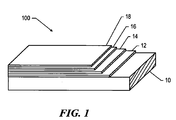
- the superconducting article includes a substrate 10, a buffer layer 12 overlying the substrate 10, a superconducting layer 14, followed by a capping layer 16, such as a noble metal, and a stabilizer layer 18, such as a non-noble metal such as copper.
- the buffer layer 12 may consist of several distinct films.
- the stabilizer layer 18 may extend around the periphery of the superconducting article 100, thereby encasing it.
- the substrate 10 is generally metal-based, and such as, an alloy of at least two metallic elements.
- Suitable substrate materials include stainless steel alloys and nickel-based metal alloys such as the known HASTELLOY® or INCONEL® group of alloys. These alloys tend to have desirable creep, chemical and mechanical properties, including coefficient of expansion, tensile strength, yield strength, and elongation. These metals are generally commercially available in the form of spooled tapes, and suitable for superconducting tape fabrication, which will utilize reel-to-reel tape handling.
- the substrate 10 is typically in a tape-like configuration, having a high dimension ratio.
- the term 'dimension ratio' is used to denote the ratio of the length of the substrate or tape to the next longest dimension, the width of the substrate or tape.
- the width of the tape is generally on the order of about 0.1 to about 10 cm, and the length of the tape is at least about 0.1 m; alternatively greater than about 5 m.
- Superconducting tapes that include substrate 10 may have a length on the order of 100 m or above. Accordingly, the substrate may have a dimension ratio which is fairly high, on the order of not less than 10, not less than about 10 2 , or even not less than about 10 3 . Certain embodiments are longer, having a dimension ratio of 10 4 and higher.
- the substrate is treated so as to have desirable surface properties for subsequent deposition of the constituent layers of the superconducting tape.
- the surface may be polished to a desired flatness and surface roughness.
- the substrate may be treated to be biaxially textured as is understood in the art, such as by the known rabits (roll assisted biaxially textured substrate) technique, although embodiments herein utilize a non-textured, polycrystalline substrate, such as commercially available nickel-based tapes noted above.
- the buffer layer may be a single layer, or more commonly, be made up of several films.
- the buffer layer includes a biaxially textured film, having a crystalline texture that is generally aligned along crystal axes both in-plane and out-of-plane of the film.
- Such biaxial texturing may be accomplished by ion beam assisted deposition (IBAD), a technique that may be advantageously utilized to form a suitably textured buffer layer for subsequent formation of a superconducting layer having desirable crystallographic orientation for superior superconducting properties.
- IBAD ion beam assisted deposition
- Magnesium oxide (MgO) is a typical material of choice for the IBAD film, and may be on the order of about 1 to about 500 nanometers, such as about 5 to about 50 nanometers.
- the IBAD film has a rock-salt like crystal structure, as defined and described in us patent 6,190,752.
- the buffer layer may include additional films, such as a barrier film provided to directly contact and be placed in between an IBAD film and the substrate.
- the barrier film may advantageously be formed of an oxide, such as yttria, and functions to isolate the substrate from the IBAD film.
- a barrier film may also be formed of non-oxides such as silicon nitride. Suitable techniques for deposition of a barrier film include chemical vapor deposition and physical vapor deposition including sputtering. Typical thicknesses of the barrier film may be within a range of about 1 to about 200 nanometers.
- the buffer layer may also include an epitaxially grown film(s), formed over the IBAD film. In this context, the epitaxially grown film is effective to increase the thickness of the IBAD film, and may desirably be made principally of the same material utilized for the IBAD layer such as MgO or other compatible materials.
- the buffer layer may further include another buffer film implemented to reduce a mismatch in lattice constants between the superconducting layer and the underlying IBAD film and/or epitaxial film.
- This buffer film may be formed of materials such as YSZ (yttria-stabilized zirconia), magnesia, ceria, gadolinium zirconium oxide, strontium ruthenate, lanthanum manganate, and generally, perovskite-structured ceramic materials.
- the buffer film may be deposited by various physical vapor deposition techniques.
- the substrate surface itself may be biaxially textured.
- the buffer layer is generally epitaxially grown on the textured substrate so as to preserve biaxial texturing in the buffer layer.
- RABITS roll assisted biaxially textured substrates
- the superconducting layer 14 is generally in the form of a high-temperature superconductor (HTS) layer.
- HTS materials are any chosen from any of the high-temperature superconducting materials that exhibit superconducting properties above the temperature of liquid nitrogen, 77k. Such materials may include, for example, YBa 2 Cu 3 O 7-x , Bi 2 Sr 2 CaCu 2 O 2 , Bi 2 Sr 2 Ca 2 Cu 3 O 10+y , Tl 2 Ba 2 Ca 2 Cu 3 O 10+y , and HgBa 2 Ca 2 Cu 3 O 8+y .
- One class of materials includes REBa 2 Cu 3 O 7-x , wherein 0 ⁇ x>1 and RE is a rare earth or combination of rare earth elements.
- YBa 2 Cu 3 O 7-x also generally referred to as YBCO
- YBCO may be used with or without the addition of dopants, such as rare earth materials, for example samarium, gadolinium, dysprosium, and holmium.
- the superconducting layer 14 may be formed by any one of various techniques, including thick and thin film forming techniques.
- a thin film physical vapor deposition technique such as pulsed laser deposition (PLD) can be used for a high deposition rates, or a chemical vapor deposition (CVD) technique can be used for lower cost and larger surface area treatment.
- PLD pulsed laser deposition
- CVD chemical vapor deposition
- the superconducting layer has a thickness on the order of about 0.1 to about 30 ⁇ m; alternatively, about 0.5 to about 20 ⁇ m, such as about 1 to about 5 ⁇ m, in order to get desirable amperage ratings associated with the superconducting layer 14.
- the HTS layer can include a prefabricated nanostructure.
- the nanostructure can include a plurality of nanorods.
- the nanorods can serve to pin magnetic flux lines of a magnetic field to reduce the effect of the magnetic field on the critical current of the superconducting article.
- the nanorods can extend at least about 50% of the thickness of the HTS layer, such as at least about 60% of the thickness of the HTS layer, such as at least about 70% of the thickness of the HTS layer, even at least about 80% of the thickness of the HTS layer.
- the nanorods can extend at least about 85% of the thickness of the HTS layer, such as at least about 90% of the thickness of the HTS layer, such as at least about 95% of the thickness of the HTS layer, even at least about 99% of the thickness of the HTS layer.
- the nanorods can have a height of between about 0.1 ⁇ m and about 10.0 ⁇ m, such as between about 1.0 ⁇ m and 3.0 ⁇ m. Further, the nanorods can have a diameter of between about 0.5 nm and about 100 nm, such as not greater than about 50 nm, even not greater than about 10 nm. In an embodiment, the nanorods can be arranged with an average spacing between adjacent nanorods of between about 0.5 times the diameter and about 100 times the diameter. In another embodiment, the average spacing may be between about 5 nm and about 50 nm. Further, the HTS layer may include not greater than about 30 vol% nanorods.
- the plurality of nanorods may be substantially parallel to one another, that is all of the plurality of nanorods can be oriented in the same direction. Alternatively, at least a portion of the plurality of nanorods may not be parallel to the other nanorods.
- the plurality of nanorods can include a first portion of nanorods oriented in a first direction and a second portion of nanorods oriented in a second direction.
- the nanorods may be oriented perpendicular to the surface of the substrate.
- the nanorods may be oriented in a direction other than perpendicular to the substrate, such as at an angle of 45°.
- the nanorods can be effective at reducing the effect of a magnetic field aligned parallel to the nanorods.
- the nanorods may be oriented in random directions. Such a structure may be preferable to achieve improved flux pinning over an entire angular range of magnetic field orientations.
- the plurality of nanorods can be arranged in an ordered array.
- an ordered array has a defined spacing between each pair of adjacent nanorods.
- the nanorods can be arranged in a square array with a substantially constant spacing between adjacent nanorods.
- the spacing between adjacent nanorods across the width of the tape may be different from the spacing between adjacent nanorods along the length.
- the plurality of nanorods can be arranged randomly.
- the density of the nanorods, the number of nanorods per square millimeter can be similar throughout the HTS layer, even when the spacing between adjacent nanorods is not constant.
- the nanorods can consist of a material other than HTS materials.
- the nanorods can include metal.
- the metal can be a ferromagnetic metal, such as iron, nickel, or cobalt, or the metal can be a non-ferromagnetic metal such as platinum or gold.
- the nanorods can include ceramic materials, such as SnO 2 , TiO 2 , ZrO 2 , LaMnO 3 or ZnO.
- the nanorods can have a metallic core surround by a ceramic layer.
- the superconducting article may also include a capping layer 16 and a stabilizer layer 18, which are generally implemented to provide a low resistance interface and for electrical stabilization to aid in prevention of superconductor burnout in practical use. Further, layers 16 and 18 aid in continued flow of electrical charges along the superconductor in cases where cooling fails or the critical current density is exceeded, and the superconducting layer moves from the superconducting state and becomes resistive.
- a noble metal is utilized for capping layer 16 to prevent unwanted interaction between the stabilizer layer(s) and the superconducting layer 14. Typical noble metals include gold, silver, platinum, and palladium. Silver is may be used due to its cost and general accessibility.
- the capping layer 16 may be made be thick enough to prevent unwanted diffusion of the components used in the application of the stabilizer layer 18 into the superconducting layer 14, but is made to be generally thin for cost reasons (raw material and processing costs).
- Various techniques may be used for deposition of the capping layer 16, including physical vapor deposition, such as dc magnetron sputtering.
- the stabilizer layer 18 is generally incorporated to overlie the superconducting layer 14, and overlie and directly contact the capping layer 16 in the embodiment shown in Figure 1 .
- the stabilizer layer 18 functions as a protection/shunt layer to enhance stability against harsh environmental conditions and superconductivity quench.
- the layer is generally dense and thermally and electrically conductive, and functions to bypass electrical current in case of failure of the superconducting layer or if the critical current of the superconducting layer is exceeded. It may be formed by any one of various thick and thin film forming techniques, such as by laminating a pre-formed copper strip onto the superconducting tape, by using an intermediary bonding material such as a solder.
- the capping layer 16 may function as a seed layer for deposition of copper thereon.
- the capping layer 16 and the stabilizer layer 18 may be altered or not used.
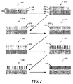
- a tape 204 can be provided.
- the tape can include substrate and buffer layers 206 and a conducting layer 208 overlying the substrate and buffer layers 206.
- the conducting layer 208 can be a thin nickel layer.
- a polymer layer 212 such as a polycarbonate film, can be deposited overtop the conducting layer 208, such as by spin coating or other coating techniques known in the art.
- the polymer layer 212 can be irradiated with an ion beam, creating damage tracks 216 within the polymer layer 212.
- high-energy particles can create a core of low molecular weight material along their path.
- Altering the duration of exposure and/or the intensity of the ion beam can control the number of damage tracks per mm 2 .
- altering the direction of bombardment of the ion beam can create nanoholes at multiple orientations. Consequently, nanorods aligned at different orientations could be created which can result in improved flux pinning over a wide angular range of magnetic field orientations.
- the polymer layer 212 can be exposed to uv radiation to further develop the damage tracks 216 within the polymer layer 212.
- the polymer layer 212 can be etched to form nanoholes 222 corresponding to the damage tracks 216 within the polymer layer 212.
- the etching chemicals can preferentially attack the damage tracks 216, removing the low molecular weight materials faster than the rest of the polymer layer 212. Altering the duration of etching can control the diameter of the nanoholes.
- the nanoholes 222 can extend through the polymer layer 212 to the conducting layer 208.
- Figure 3a shows a micrograph of the nanoholes formed through the polymer layer 212.
- metal such as nickel or gold
- metal can be electroplated within the nanoholes 222 to form nanorods 226 extending from the conducting layer 208 through the polymer layer 212.
- the polymer layer 212 can be exposed to an additional etching process to completely remove the remaining polymer layer 212, leaving the nanorods 226 intact.
- Figure 3b and Figure 3c show micrographs of nanorods.
- HTS material can be deposited to form an HTS layer surrounding the nanorods 226.
- the HTS material can be deposited using one of the various techniques known in the art, including PLD, CVD, spray pyrolysis, and the like.
- the conducting layer can be oxidized, such as to form nickel oxide, prior to the deposition of the HTS material. Additionally, a layer of lamno 3 may be deposited overtop the nickel oxide prior to the deposition of the HTS material.
- nanorods can be formed using a nanoporous template.
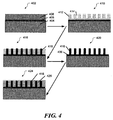
- Figure 4 illustrates an exemplary process of using nanoporous templates to form a prefabricated nanostructure with the HTS layer.
- a substrate 404 and a buffer layer 406 are provided.
- an aluminum layer 408 is deposited overtop the buffer layer 406.
- the aluminum layer can be deposited by sputtering or thermal evaporation.
- an anodic oxidation process can convert the aluminum layer 408 into an anodized aluminum oxide layer 412 including a highly ordered array of nanopores 414.
- metal such as nickel or gold, can be electrodeposited within the nanopores 414 forming nanorods 418.
- HTS material can be deposited to form an HTS layer 426 surrounding the nanorods 418.
- the HTS material can be deposited using one of the various techniques known in the art, including PLD, CVD, spray pyrolysis, and the like.
- inorganic nanotemplates can be used during the process of forming the nanorods.
- aluminum and silicon can be sputtered onto the buffer layer to form aluminum nanorods embedded within a silicon matrix.
- the aluminum can be preferentially etched leaving nanopores within the silicon matrix.
- chemical vapor deposition or chemical solution deposition can be used to form nanorods on predefined nucleation sites.
- a nanodot array using materials such as colloidal gold particles or similar material can be deposited on the buffer surface as a nucleation site for the nanorods.
- Vapor-solid-liquid phase growth can be employed to grow the nanorods using the nanodots as a nucleation site.
- ZnO can be mixed with graphite and vaporized.
- the vaporized material can be deposited on the nanodot templates.
- the spacing and density of the nanorods can depend on the spacing and density of the nanodots.
- the diameter and length of the nanorods can depend on the vaporization temperature and time and the deposition temperature and time. Other materials such as magnetic oxides can be used to form the nanorods that could lead to ferromagnetic pinning.
- HTS material can be deposited around the nanorods to form an HTS layer embedding the nanorods. Since the nanorods are formed without the need for a nanoporous mask or template, no etching process may be needed to remove the mask or template from the buffer surface after the growth of the nanorods. Accordingly, the CVD nanorod deposition can be performed in an upstream portion of a CVD reactor used for depositing the HTS layer.
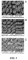
- Figures 5a-5c show micrographs of the ZnO nanostructures formed by CVD.
- Figures 5a and 5b show a faceted, plate-like nanostructure formed without the use of gold nanodots.
- Figure 5c shows ZnO nanorods formed on a buffered template on a flexible metal substrate using CVD.
- nanorods can be formed using a high energy, focused electron beam.
- the tape including the substrate and the buffer layers, can be within a vacuum chamber.
- the nanorod material can be evaporated into the atmosphere surrounding the substrate.
- An electron beam can be focused on the surface of the buffer layer, forcing any nanorod material crossing the path of the electron beam to be deposited on the buffer layer.
- the electron beam can be focused to a spot on the order of a few nanometers, resulting in the deposition of nanorods having a diameter of a few nanometers. Modifying the electron beam size, current density, concentration of nanorod material, and exposure time can control the length and diameter of the nanorods.
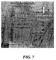
- FIGS. 6a-6c show micrographs of the platinum nanorods formed using a focused electron beam.
- Figure 6a shows the nanorod array from above and
- Figure 6b shows the nanorod array in a 52° inclined view.
- Figure 6c shows a single nanorod of the array having a diameter of about 100 nm and a length of about 600 nm.
- the nanorods can be formed from or coated with an oxides compatible with the HTS material and the HTS material fabrication.
- the oxide such as LaMnO 3
- the oxide layer can match the lattice properties of the HTS layer, reducing lattice mismatch effects.
- the nanorods can induce strain in the interface between the HTS layer and the nanorods, resulting in additional pinning.
- magnetic pinning can be accomplished using ferromagnetic nanorods surrounded by metal oxide nanotubes.
- the nanotubes can prevent the ferromagnetic material, such as iron or nickel, from interacting with the HTS material.
- the nanotubes can have a lattice mismatch, structural mismatch, or a thermal expansion coefficient mismatch with the HTS material, thus inducing interfacial strain between the HTS material and the nanotube.
- the interfacial strain can act to further pin magnetic field lines.
- the nanotubes can be formed from ZnO which has a hexagonal structure, compared to the orthorhombic perovskite structure of an HTS material such as YBCQ.
- the spacing of the nanorods can be selected to correspond to the strength of an applied magnetic field.
- the density of the nanorods can be chosen to match the density of the magnetic flux lines.
- a superconducting article for use in a 1 t field can have a spacing of about 40 nm between adjacent nanorods
- a superconducting article for use in a 5 t magnetic field can have a spacing of about 20 nm between adjacent nanorods
- a superconducting article for use in a 15 t field can have a spacing of about 10 nm between adjacent nanorods.
- the plurality of nanorods can include a first subset of nanorods and a second subset of nanorods.
- the second subset of nanorods can be interspersed among the first subset of nanorods.
- the second subset of nanorods may have a different orientation a different spacing, different diameter, different height, a different material, or any combination thereof compared to the first subset of nanorods.
- the first subset of nanorods can oriented to extend vertically from the surface of the buffer layer and the second subset of nanorods can be oriented at a 45° angle from the surface of the buffer layer.
- the HTS material can be deposited overtop the buffer layer and surrounding the nanorods.
- the HTS material may be deposited using a variety of techniques known in the art, including PLD, CVD, MOCVD (metal-organic CVD), and spray pyrolysis.
- Deposition techniques such as PLD and MOCVD that can deposit a superconductor layer relatively high rate.
- MOCVD can be used to deposit HTS material at a rate of at least about 5 ⁇ m per hour, such as at least about 10 ⁇ m per hour, even at least about 30 ⁇ m per hour. Due to the prefabrication of the nanorods, changes to the deposition process can be minimized, including maintaining the deposition at a relative high rate.
- a long length substrate can be translated through a deposition zone at a rate of at least about 10 meters per hour, such as at least about 30 meters per hour, even at least about 50 meters per hour.
- any number falling within the range is specifically disclosed.
- any numerical range defined by two r numbers as defined in the above is also specifically disclosed.
Landscapes
- Chemical & Material Sciences (AREA)
- Engineering & Computer Science (AREA)
- Inorganic Chemistry (AREA)
- Manufacturing & Machinery (AREA)
- Materials Engineering (AREA)
- Nanotechnology (AREA)
- Chemical Kinetics & Catalysis (AREA)
- Mechanical Engineering (AREA)
- Metallurgy (AREA)
- Organic Chemistry (AREA)
- Crystallography & Structural Chemistry (AREA)
- Ceramic Engineering (AREA)
- Physics & Mathematics (AREA)
- Condensed Matter Physics & Semiconductors (AREA)
- General Physics & Mathematics (AREA)
- Composite Materials (AREA)
- Superconductors And Manufacturing Methods Therefor (AREA)
- Containers, Films, And Cooling For Superconductive Devices (AREA)
- Superconductor Devices And Manufacturing Methods Thereof (AREA)
Applications Claiming Priority (2)
| Application Number | Priority Date | Filing Date | Title |
|---|---|---|---|
| US22922509P | 2009-07-28 | 2009-07-28 | |
| PCT/US2010/043411 WO2011017112A2 (en) | 2009-07-28 | 2010-07-27 | Superconducting article with prefabricated nanostructure for improved flux pinning |
Publications (3)
| Publication Number | Publication Date |
|---|---|
| EP2460197A2 EP2460197A2 (en) | 2012-06-06 |
| EP2460197A4 EP2460197A4 (en) | 2014-01-15 |
| EP2460197B1 true EP2460197B1 (en) | 2016-03-16 |
Family
ID=43527576
Family Applications (1)
| Application Number | Title | Priority Date | Filing Date |
|---|---|---|---|
| EP10806895.8A Active EP2460197B1 (en) | 2009-07-28 | 2010-07-27 | Superconducting article with prefabricated nanostructure for improved flux pinning |
Country Status (8)
| Country | Link |
|---|---|
| US (1) | US8926868B2 (enExample) |
| EP (1) | EP2460197B1 (enExample) |
| JP (1) | JP5858912B2 (enExample) |
| KR (1) | KR101485060B1 (enExample) |
| CN (2) | CN102484197B (enExample) |
| CA (1) | CA2768516C (enExample) |
| IN (1) | IN2012DN00641A (enExample) |
| WO (1) | WO2011017112A2 (enExample) |
Families Citing this family (13)
| Publication number | Priority date | Publication date | Assignee | Title |
|---|---|---|---|---|
| US7442629B2 (en) * | 2004-09-24 | 2008-10-28 | President & Fellows Of Harvard College | Femtosecond laser-induced formation of submicrometer spikes on a semiconductor substrate |
| TW201228985A (en) * | 2011-01-05 | 2012-07-16 | Univ Nat Cheng Kung | Nanorod-containing precursor powder, nanorod-containing superconductor bulk and method for manufacturing the same |
| US9362025B1 (en) | 2012-02-08 | 2016-06-07 | Superconductor Technologies, Inc. | Coated conductor high temperature superconductor carrying high critical current under magnetic field by intrinsic pinning centers, and methods of manufacture of same |
| US9564258B2 (en) | 2012-02-08 | 2017-02-07 | Superconductor Technologies, Inc. | Coated conductor high temperature superconductor carrying high critical current under magnetic field by intrinsic pinning centers, and methods of manufacture of same |
| DE102013210940B3 (de) * | 2013-06-12 | 2014-07-03 | THEVA DüNNSCHICHTTECHNIK GMBH | Beschichtung technischer Substrate zur Herstellung supraleitender Schichten mit hoher Sprungtemperatur |
| US9410394B2 (en) | 2013-12-11 | 2016-08-09 | Schlumberger Technology Corporation | Methods for minimizing overdisplacement of proppant in fracture treatments |
| WO2016149543A1 (en) * | 2015-03-17 | 2016-09-22 | The University Of Houston System | Improved superconductor compositions |
| WO2017217487A1 (ja) * | 2016-06-16 | 2017-12-21 | 株式会社フジクラ | 酸化物超電導線材及びその製造方法 |
| CN108963067B (zh) * | 2018-07-27 | 2022-04-29 | 武汉工程大学 | 一种ReBa2Cu3O7-x超导薄膜上制备钉扎层的方法 |
| WO2020117369A2 (en) | 2018-10-14 | 2020-06-11 | Metal Oxide Technologies, Llc. | Superconductor flux pinning without columnar defects |
| EP3928359B8 (en) * | 2019-02-18 | 2025-08-06 | Superpower, Inc. | Superconductor wire and fabrication thereof |
| CN110444658B (zh) * | 2019-08-13 | 2020-08-11 | 中国科学院上海微系统与信息技术研究所 | 基于AlMn合金超导薄膜的TES微量能器及制备方法 |
| US20230031577A1 (en) * | 2021-07-08 | 2023-02-02 | Superq Technologies India Pvt Ltd | Method and systems for fabricating superconducting nanowire single photon detector (snspd) |
Citations (1)
| Publication number | Priority date | Publication date | Assignee | Title |
|---|---|---|---|---|
| WO2009012459A2 (en) * | 2007-07-19 | 2009-01-22 | California Institute Of Technology | Structures of ordered arrays of semiconductors |
Family Cites Families (16)
| Publication number | Priority date | Publication date | Assignee | Title |
|---|---|---|---|---|
| JPH0262083A (ja) | 1988-08-29 | 1990-03-01 | Canon Inc | ジョセフソン接合の形成方法およびジョセフソン接合素子 |
| EP0553593B1 (en) | 1992-01-28 | 1996-05-29 | International Business Machines Corporation | Pinning structures for superconducting films and method for making same |
| JP2747173B2 (ja) * | 1992-08-07 | 1998-05-06 | 日本電信電話株式会社 | 酸化物高温超伝導体単結晶薄膜形成方法 |
| DE69403104T2 (de) | 1993-02-15 | 1997-10-30 | Sumitomo Electric Industries | Verfahren zum Erzeugen einer strukturierten oxydsupraleitenden Dünnschicht |
| US5897945A (en) | 1996-02-26 | 1999-04-27 | President And Fellows Of Harvard College | Metal oxide nanorods |
| US6190752B1 (en) | 1997-11-13 | 2001-02-20 | Board Of Trustees Of The Leland Stanford Junior University | Thin films having rock-salt-like structure deposited on amorphous surfaces |
| US8119571B2 (en) | 2006-08-03 | 2012-02-21 | Amit Goyal | High performance electrical, magnetic, electromagnetic and electrooptical devices enabled by three dimensionally ordered nanodots and nanorods |
| JP3622147B2 (ja) * | 2001-06-19 | 2005-02-23 | 独立行政法人産業技術総合研究所 | 柱状ピン止め中心を有する超伝導薄膜及びその製造方法 |
| US20040266628A1 (en) * | 2003-06-27 | 2004-12-30 | Superpower, Inc. | Novel superconducting articles, and methods for forming and using same |
| JP4495426B2 (ja) * | 2003-08-29 | 2010-07-07 | 独立行政法人科学技術振興機構 | 超伝導膜およびその製造方法 |
| US8178165B2 (en) | 2005-01-21 | 2012-05-15 | The Regents Of The University Of California | Method for fabricating a long-range ordered periodic array of nano-features, and articles comprising same |
| JP2006233247A (ja) | 2005-02-23 | 2006-09-07 | Fujikura Ltd | 薄膜形成装置 |
| US8034745B2 (en) | 2005-08-01 | 2011-10-11 | Amit Goyal | High performance devices enabled by epitaxial, preferentially oriented, nanodots and/or nanorods |
| US20070238619A1 (en) * | 2005-09-06 | 2007-10-11 | Superpower, Inc. | Superconductor components |
| JP5017161B2 (ja) | 2008-03-27 | 2012-09-05 | 株式会社東芝 | 酸化物超電導体 |
| US7919435B2 (en) | 2008-09-30 | 2011-04-05 | Ut-Battelle, Llc | Superconductor films with improved flux pinning and reduced AC losses |
-
2010
- 2010-07-27 JP JP2012522973A patent/JP5858912B2/ja active Active
- 2010-07-27 IN IN641DEN2012 patent/IN2012DN00641A/en unknown
- 2010-07-27 EP EP10806895.8A patent/EP2460197B1/en active Active
- 2010-07-27 US US12/844,432 patent/US8926868B2/en active Active
- 2010-07-27 CN CN201080038345.6A patent/CN102484197B/zh active Active
- 2010-07-27 CN CN201610511799.XA patent/CN106065474B/zh active Active
- 2010-07-27 CA CA2768516A patent/CA2768516C/en active Active
- 2010-07-27 KR KR1020127003750A patent/KR101485060B1/ko active Active
- 2010-07-27 WO PCT/US2010/043411 patent/WO2011017112A2/en not_active Ceased
Patent Citations (1)
| Publication number | Priority date | Publication date | Assignee | Title |
|---|---|---|---|---|
| WO2009012459A2 (en) * | 2007-07-19 | 2009-01-22 | California Institute Of Technology | Structures of ordered arrays of semiconductors |
Also Published As
| Publication number | Publication date |
|---|---|
| WO2011017112A3 (en) | 2011-04-28 |
| JP5858912B2 (ja) | 2016-02-10 |
| IN2012DN00641A (enExample) | 2015-08-21 |
| CN102484197B (zh) | 2016-08-10 |
| CN106065474B (zh) | 2019-05-28 |
| KR20120051688A (ko) | 2012-05-22 |
| EP2460197A2 (en) | 2012-06-06 |
| CN102484197A (zh) | 2012-05-30 |
| WO2011017112A2 (en) | 2011-02-10 |
| US8926868B2 (en) | 2015-01-06 |
| CA2768516A1 (en) | 2011-02-10 |
| EP2460197A4 (en) | 2014-01-15 |
| KR101485060B1 (ko) | 2015-01-21 |
| CA2768516C (en) | 2015-07-14 |
| JP2013501313A (ja) | 2013-01-10 |
| CN106065474A (zh) | 2016-11-02 |
| US20110028328A1 (en) | 2011-02-03 |
Similar Documents
| Publication | Publication Date | Title |
|---|---|---|
| EP2460197B1 (en) | Superconducting article with prefabricated nanostructure for improved flux pinning | |
| US8682406B2 (en) | Multifilament superconductor having reduced AC losses and method for forming the same | |
| EP2245638B1 (en) | Method of forming an hts article | |
| WO2015054119A1 (en) | Coated conductor high temperature superconductors with intrinsic pinning centers | |
| US11488746B2 (en) | Superconductor with improved flux pinning at low temperatures | |
| JP2016522534A5 (enExample) | ||
| JP2009503792A (ja) | Ybco被覆において高い臨界電流密度の改良された構造体 | |
| US7445808B2 (en) | Method of forming a superconducting article | |
| KR101318128B1 (ko) | 초전도성 물품의 안티에피택셜 막과 관련 물품, 디바이스및 시스템 | |
| US7618923B2 (en) | Method for making a superconductor with improved microstructure |
Legal Events
| Date | Code | Title | Description |
|---|---|---|---|
| PUAI | Public reference made under article 153(3) epc to a published international application that has entered the european phase |
Free format text: ORIGINAL CODE: 0009012 |
|
| 17P | Request for examination filed |
Effective date: 20120220 |
|
| AK | Designated contracting states |
Kind code of ref document: A2 Designated state(s): AL AT BE BG CH CY CZ DE DK EE ES FI FR GB GR HR HU IE IS IT LI LT LU LV MC MK MT NL NO PL PT RO SE SI SK SM TR |
|
| RIN1 | Information on inventor provided before grant (corrected) |
Inventor name: MARCHEVSKY, MAXIM Inventor name: MAJKIC, GORAN Inventor name: SELVAMANICKAM, VENKAT |
|
| DAX | Request for extension of the european patent (deleted) | ||
| A4 | Supplementary search report drawn up and despatched |
Effective date: 20131213 |
|
| RIC1 | Information provided on ipc code assigned before grant |
Ipc: B82B 3/00 20060101ALI20131209BHEP Ipc: C23C 14/04 20060101ALI20131209BHEP Ipc: B82Y 40/00 20110101ALI20131209BHEP Ipc: H01L 39/24 20060101AFI20131209BHEP Ipc: H01L 39/14 20060101ALI20131209BHEP |
|
| 17Q | First examination report despatched |
Effective date: 20141120 |
|
| RIC1 | Information provided on ipc code assigned before grant |
Ipc: B82Y 40/00 20110101ALN20150417BHEP Ipc: C23C 28/00 20060101ALI20150417BHEP Ipc: H01L 39/24 20060101AFI20150417BHEP Ipc: H01L 39/14 20060101ALI20150417BHEP Ipc: B82Y 30/00 20110101ALN20150417BHEP |
|
| GRAP | Despatch of communication of intention to grant a patent |
Free format text: ORIGINAL CODE: EPIDOSNIGR1 |
|
| RIC1 | Information provided on ipc code assigned before grant |
Ipc: H01L 39/14 20060101ALI20150512BHEP Ipc: B82Y 40/00 20110101ALN20150512BHEP Ipc: C23C 28/00 20060101ALI20150512BHEP Ipc: H01L 39/24 20060101AFI20150512BHEP Ipc: B82Y 30/00 20110101ALN20150512BHEP |
|
| INTG | Intention to grant announced |
Effective date: 20150610 |
|
| GRAS | Grant fee paid |
Free format text: ORIGINAL CODE: EPIDOSNIGR3 |
|
| RIC1 | Information provided on ipc code assigned before grant |
Ipc: B82Y 40/00 20110101ALN20151029BHEP Ipc: H01L 39/24 20060101AFI20151029BHEP Ipc: H01L 39/14 20060101ALI20151029BHEP Ipc: C23C 28/00 20060101ALI20151029BHEP Ipc: B82Y 30/00 20110101ALN20151029BHEP |
|
| REG | Reference to a national code |
Ref country code: DE Ref legal event code: R079 Ref document number: 602010031280 Country of ref document: DE Free format text: PREVIOUS MAIN CLASS: H01L0039020000 Ipc: H01L0039240000 |
|
| GRAA | (expected) grant |
Free format text: ORIGINAL CODE: 0009210 |
|
| INTG | Intention to grant announced |
Effective date: 20160114 |
|
| RIC1 | Information provided on ipc code assigned before grant |
Ipc: H01L 39/24 20060101AFI20160112BHEP Ipc: B82Y 40/00 20110101ALN20160112BHEP Ipc: H01L 39/14 20060101ALI20160112BHEP Ipc: B82Y 30/00 20110101ALN20160112BHEP Ipc: C23C 28/00 20060101ALI20160112BHEP |
|
| AK | Designated contracting states |
Kind code of ref document: B1 Designated state(s): AL AT BE BG CH CY CZ DE DK EE ES FI FR GB GR HR HU IE IS IT LI LT LU LV MC MK MT NL NO PL PT RO SE SI SK SM TR |
|
| REG | Reference to a national code |
Ref country code: GB Ref legal event code: FG4D |
|
| REG | Reference to a national code |
Ref country code: CH Ref legal event code: EP |
|
| REG | Reference to a national code |
Ref country code: IE Ref legal event code: FG4D |
|
| REG | Reference to a national code |
Ref country code: AT Ref legal event code: REF Ref document number: 781904 Country of ref document: AT Kind code of ref document: T Effective date: 20160415 |
|
| REG | Reference to a national code |
Ref country code: DE Ref legal event code: R096 Ref document number: 602010031280 Country of ref document: DE |
|
| REG | Reference to a national code |
Ref country code: NL Ref legal event code: MP Effective date: 20160316 |
|
| REG | Reference to a national code |
Ref country code: LT Ref legal event code: MG4D |
|
| REG | Reference to a national code |
Ref country code: FR Ref legal event code: PLFP Year of fee payment: 7 |
|
| PG25 | Lapsed in a contracting state [announced via postgrant information from national office to epo] |
Ref country code: NO Free format text: LAPSE BECAUSE OF FAILURE TO SUBMIT A TRANSLATION OF THE DESCRIPTION OR TO PAY THE FEE WITHIN THE PRESCRIBED TIME-LIMIT Effective date: 20160616 Ref country code: HR Free format text: LAPSE BECAUSE OF FAILURE TO SUBMIT A TRANSLATION OF THE DESCRIPTION OR TO PAY THE FEE WITHIN THE PRESCRIBED TIME-LIMIT Effective date: 20160316 Ref country code: FI Free format text: LAPSE BECAUSE OF FAILURE TO SUBMIT A TRANSLATION OF THE DESCRIPTION OR TO PAY THE FEE WITHIN THE PRESCRIBED TIME-LIMIT Effective date: 20160316 Ref country code: GR Free format text: LAPSE BECAUSE OF FAILURE TO SUBMIT A TRANSLATION OF THE DESCRIPTION OR TO PAY THE FEE WITHIN THE PRESCRIBED TIME-LIMIT Effective date: 20160617 |
|
| REG | Reference to a national code |
Ref country code: AT Ref legal event code: MK05 Ref document number: 781904 Country of ref document: AT Kind code of ref document: T Effective date: 20160316 |
|
| PG25 | Lapsed in a contracting state [announced via postgrant information from national office to epo] |
Ref country code: NL Free format text: LAPSE BECAUSE OF FAILURE TO SUBMIT A TRANSLATION OF THE DESCRIPTION OR TO PAY THE FEE WITHIN THE PRESCRIBED TIME-LIMIT Effective date: 20160316 Ref country code: LV Free format text: LAPSE BECAUSE OF FAILURE TO SUBMIT A TRANSLATION OF THE DESCRIPTION OR TO PAY THE FEE WITHIN THE PRESCRIBED TIME-LIMIT Effective date: 20160316 Ref country code: LT Free format text: LAPSE BECAUSE OF FAILURE TO SUBMIT A TRANSLATION OF THE DESCRIPTION OR TO PAY THE FEE WITHIN THE PRESCRIBED TIME-LIMIT Effective date: 20160316 Ref country code: SE Free format text: LAPSE BECAUSE OF FAILURE TO SUBMIT A TRANSLATION OF THE DESCRIPTION OR TO PAY THE FEE WITHIN THE PRESCRIBED TIME-LIMIT Effective date: 20160316 |
|
| PG25 | Lapsed in a contracting state [announced via postgrant information from national office to epo] |
Ref country code: PL Free format text: LAPSE BECAUSE OF FAILURE TO SUBMIT A TRANSLATION OF THE DESCRIPTION OR TO PAY THE FEE WITHIN THE PRESCRIBED TIME-LIMIT Effective date: 20160316 Ref country code: EE Free format text: LAPSE BECAUSE OF FAILURE TO SUBMIT A TRANSLATION OF THE DESCRIPTION OR TO PAY THE FEE WITHIN THE PRESCRIBED TIME-LIMIT Effective date: 20160316 Ref country code: IS Free format text: LAPSE BECAUSE OF FAILURE TO SUBMIT A TRANSLATION OF THE DESCRIPTION OR TO PAY THE FEE WITHIN THE PRESCRIBED TIME-LIMIT Effective date: 20160716 |
|
| PG25 | Lapsed in a contracting state [announced via postgrant information from national office to epo] |
Ref country code: PT Free format text: LAPSE BECAUSE OF FAILURE TO SUBMIT A TRANSLATION OF THE DESCRIPTION OR TO PAY THE FEE WITHIN THE PRESCRIBED TIME-LIMIT Effective date: 20160718 Ref country code: RO Free format text: LAPSE BECAUSE OF FAILURE TO SUBMIT A TRANSLATION OF THE DESCRIPTION OR TO PAY THE FEE WITHIN THE PRESCRIBED TIME-LIMIT Effective date: 20160316 Ref country code: ES Free format text: LAPSE BECAUSE OF FAILURE TO SUBMIT A TRANSLATION OF THE DESCRIPTION OR TO PAY THE FEE WITHIN THE PRESCRIBED TIME-LIMIT Effective date: 20160316 Ref country code: SK Free format text: LAPSE BECAUSE OF FAILURE TO SUBMIT A TRANSLATION OF THE DESCRIPTION OR TO PAY THE FEE WITHIN THE PRESCRIBED TIME-LIMIT Effective date: 20160316 Ref country code: CZ Free format text: LAPSE BECAUSE OF FAILURE TO SUBMIT A TRANSLATION OF THE DESCRIPTION OR TO PAY THE FEE WITHIN THE PRESCRIBED TIME-LIMIT Effective date: 20160316 Ref country code: SM Free format text: LAPSE BECAUSE OF FAILURE TO SUBMIT A TRANSLATION OF THE DESCRIPTION OR TO PAY THE FEE WITHIN THE PRESCRIBED TIME-LIMIT Effective date: 20160316 Ref country code: AT Free format text: LAPSE BECAUSE OF FAILURE TO SUBMIT A TRANSLATION OF THE DESCRIPTION OR TO PAY THE FEE WITHIN THE PRESCRIBED TIME-LIMIT Effective date: 20160316 |
|
| REG | Reference to a national code |
Ref country code: DE Ref legal event code: R097 Ref document number: 602010031280 Country of ref document: DE |
|
| PG25 | Lapsed in a contracting state [announced via postgrant information from national office to epo] |
Ref country code: BE Free format text: LAPSE BECAUSE OF FAILURE TO SUBMIT A TRANSLATION OF THE DESCRIPTION OR TO PAY THE FEE WITHIN THE PRESCRIBED TIME-LIMIT Effective date: 20160316 Ref country code: IT Free format text: LAPSE BECAUSE OF FAILURE TO SUBMIT A TRANSLATION OF THE DESCRIPTION OR TO PAY THE FEE WITHIN THE PRESCRIBED TIME-LIMIT Effective date: 20160316 |
|
| PLBE | No opposition filed within time limit |
Free format text: ORIGINAL CODE: 0009261 |
|
| STAA | Information on the status of an ep patent application or granted ep patent |
Free format text: STATUS: NO OPPOSITION FILED WITHIN TIME LIMIT |
|
| PG25 | Lapsed in a contracting state [announced via postgrant information from national office to epo] |
Ref country code: DK Free format text: LAPSE BECAUSE OF FAILURE TO SUBMIT A TRANSLATION OF THE DESCRIPTION OR TO PAY THE FEE WITHIN THE PRESCRIBED TIME-LIMIT Effective date: 20160316 |
|
| 26N | No opposition filed |
Effective date: 20161219 |
|
| PG25 | Lapsed in a contracting state [announced via postgrant information from national office to epo] |
Ref country code: BG Free format text: LAPSE BECAUSE OF FAILURE TO SUBMIT A TRANSLATION OF THE DESCRIPTION OR TO PAY THE FEE WITHIN THE PRESCRIBED TIME-LIMIT Effective date: 20160616 |
|
| REG | Reference to a national code |
Ref country code: CH Ref legal event code: PL |
|
| PG25 | Lapsed in a contracting state [announced via postgrant information from national office to epo] |
Ref country code: MC Free format text: LAPSE BECAUSE OF FAILURE TO SUBMIT A TRANSLATION OF THE DESCRIPTION OR TO PAY THE FEE WITHIN THE PRESCRIBED TIME-LIMIT Effective date: 20160316 |
|
| PG25 | Lapsed in a contracting state [announced via postgrant information from national office to epo] |
Ref country code: LI Free format text: LAPSE BECAUSE OF NON-PAYMENT OF DUE FEES Effective date: 20160731 Ref country code: CH Free format text: LAPSE BECAUSE OF NON-PAYMENT OF DUE FEES Effective date: 20160731 |
|
| REG | Reference to a national code |
Ref country code: IE Ref legal event code: MM4A |
|
| PG25 | Lapsed in a contracting state [announced via postgrant information from national office to epo] |
Ref country code: SI Free format text: LAPSE BECAUSE OF FAILURE TO SUBMIT A TRANSLATION OF THE DESCRIPTION OR TO PAY THE FEE WITHIN THE PRESCRIBED TIME-LIMIT Effective date: 20160316 |
|
| REG | Reference to a national code |
Ref country code: FR Ref legal event code: PLFP Year of fee payment: 8 |
|
| PG25 | Lapsed in a contracting state [announced via postgrant information from national office to epo] |
Ref country code: IE Free format text: LAPSE BECAUSE OF NON-PAYMENT OF DUE FEES Effective date: 20160727 |
|
| PG25 | Lapsed in a contracting state [announced via postgrant information from national office to epo] |
Ref country code: LU Free format text: LAPSE BECAUSE OF NON-PAYMENT OF DUE FEES Effective date: 20160727 |
|
| PG25 | Lapsed in a contracting state [announced via postgrant information from national office to epo] |
Ref country code: CY Free format text: LAPSE BECAUSE OF FAILURE TO SUBMIT A TRANSLATION OF THE DESCRIPTION OR TO PAY THE FEE WITHIN THE PRESCRIBED TIME-LIMIT Effective date: 20160316 Ref country code: HU Free format text: LAPSE BECAUSE OF FAILURE TO SUBMIT A TRANSLATION OF THE DESCRIPTION OR TO PAY THE FEE WITHIN THE PRESCRIBED TIME-LIMIT; INVALID AB INITIO Effective date: 20100727 |
|
| PG25 | Lapsed in a contracting state [announced via postgrant information from national office to epo] |
Ref country code: TR Free format text: LAPSE BECAUSE OF FAILURE TO SUBMIT A TRANSLATION OF THE DESCRIPTION OR TO PAY THE FEE WITHIN THE PRESCRIBED TIME-LIMIT Effective date: 20160316 Ref country code: MK Free format text: LAPSE BECAUSE OF FAILURE TO SUBMIT A TRANSLATION OF THE DESCRIPTION OR TO PAY THE FEE WITHIN THE PRESCRIBED TIME-LIMIT Effective date: 20160316 Ref country code: MT Free format text: LAPSE BECAUSE OF NON-PAYMENT OF DUE FEES Effective date: 20160731 |
|
| REG | Reference to a national code |
Ref country code: FR Ref legal event code: PLFP Year of fee payment: 9 |
|
| PG25 | Lapsed in a contracting state [announced via postgrant information from national office to epo] |
Ref country code: AL Free format text: LAPSE BECAUSE OF FAILURE TO SUBMIT A TRANSLATION OF THE DESCRIPTION OR TO PAY THE FEE WITHIN THE PRESCRIBED TIME-LIMIT Effective date: 20160316 |
|
| REG | Reference to a national code |
Ref country code: GB Ref legal event code: S117 Free format text: REQUEST FILED; REQUEST FOR CORRECTION UNDER SECTION 117 FILED ON 20 MARCH 2019 |
|
| REG | Reference to a national code |
Ref country code: GB Ref legal event code: S117 Free format text: CORRECTIONS ALLOWED; REQUEST FOR CORRECTION UNDER SECTION 117 FILED ON 20 MARCH 2019 ALLOWED ON 25 APRIL 2019 |
|
| REG | Reference to a national code |
Ref country code: DE Ref legal event code: R079 Ref document number: 602010031280 Country of ref document: DE Free format text: PREVIOUS MAIN CLASS: H01L0039240000 Ipc: H10N0060010000 |
|
| P01 | Opt-out of the competence of the unified patent court (upc) registered |
Effective date: 20230530 |
|
| PGFP | Annual fee paid to national office [announced via postgrant information from national office to epo] |
Ref country code: DE Payment date: 20250729 Year of fee payment: 16 |
|
| PGFP | Annual fee paid to national office [announced via postgrant information from national office to epo] |
Ref country code: GB Payment date: 20250728 Year of fee payment: 16 |
|
| PGFP | Annual fee paid to national office [announced via postgrant information from national office to epo] |
Ref country code: FR Payment date: 20250728 Year of fee payment: 16 |