EP2446287B1 - Circuits and methods for generating a diagnostic mode of operation in a magnetic field sensor - Google Patents
Circuits and methods for generating a diagnostic mode of operation in a magnetic field sensor Download PDFInfo
- Publication number
- EP2446287B1 EP2446287B1 EP10739429.8A EP10739429A EP2446287B1 EP 2446287 B1 EP2446287 B1 EP 2446287B1 EP 10739429 A EP10739429 A EP 10739429A EP 2446287 B1 EP2446287 B1 EP 2446287B1
- Authority
- EP
- European Patent Office
- Prior art keywords
- magnetic field
- diagnostic
- sensing elements
- signal
- field sensor
- Prior art date
- Legal status (The legal status is an assumption and is not a legal conclusion. Google has not performed a legal analysis and makes no representation as to the accuracy of the status listed.)
- Active
Links
- 230000005291 magnetic effect Effects 0.000 title claims abstract description 452
- 238000000034 method Methods 0.000 title claims description 16
- 238000012360 testing method Methods 0.000 claims abstract description 78
- 239000004020 conductor Substances 0.000 claims description 68
- 230000004044 response Effects 0.000 claims description 23
- 239000000758 substrate Substances 0.000 claims description 21
- 230000008878 coupling Effects 0.000 claims description 11
- 238000010168 coupling process Methods 0.000 claims description 11
- 238000005859 coupling reaction Methods 0.000 claims description 11
- 229910052751 metal Inorganic materials 0.000 claims description 11
- 239000002184 metal Substances 0.000 claims description 11
- 238000012545 processing Methods 0.000 claims description 5
- 230000005355 Hall effect Effects 0.000 description 117
- 238000010586 diagram Methods 0.000 description 28
- 230000035945 sensitivity Effects 0.000 description 10
- 238000001228 spectrum Methods 0.000 description 7
- 230000005294 ferromagnetic effect Effects 0.000 description 6
- 230000006870 function Effects 0.000 description 6
- PXHVJJICTQNCMI-UHFFFAOYSA-N Nickel Chemical compound [Ni] PXHVJJICTQNCMI-UHFFFAOYSA-N 0.000 description 4
- 238000005259 measurement Methods 0.000 description 4
- 230000008859 change Effects 0.000 description 3
- 230000000694 effects Effects 0.000 description 3
- 238000004519 manufacturing process Methods 0.000 description 3
- 230000003595 spectral effect Effects 0.000 description 3
- 230000000295 complement effect Effects 0.000 description 2
- 230000004907 flux Effects 0.000 description 2
- WPYVAWXEWQSOGY-UHFFFAOYSA-N indium antimonide Chemical compound [Sb]#[In] WPYVAWXEWQSOGY-UHFFFAOYSA-N 0.000 description 2
- 229910052759 nickel Inorganic materials 0.000 description 2
- 230000005641 tunneling Effects 0.000 description 2
- VYZAMTAEIAYCRO-UHFFFAOYSA-N Chromium Chemical compound [Cr] VYZAMTAEIAYCRO-UHFFFAOYSA-N 0.000 description 1
- RYGMFSIKBFXOCR-UHFFFAOYSA-N Copper Chemical compound [Cu] RYGMFSIKBFXOCR-UHFFFAOYSA-N 0.000 description 1
- RTAQQCXQSZGOHL-UHFFFAOYSA-N Titanium Chemical compound [Ti] RTAQQCXQSZGOHL-UHFFFAOYSA-N 0.000 description 1
- 229910052782 aluminium Inorganic materials 0.000 description 1
- XAGFODPZIPBFFR-UHFFFAOYSA-N aluminium Chemical compound [Al] XAGFODPZIPBFFR-UHFFFAOYSA-N 0.000 description 1
- 230000006399 behavior Effects 0.000 description 1
- 239000003990 capacitor Substances 0.000 description 1
- 229910052804 chromium Inorganic materials 0.000 description 1
- 239000011651 chromium Substances 0.000 description 1
- 239000012141 concentrate Substances 0.000 description 1
- 229910052802 copper Inorganic materials 0.000 description 1
- 239000010949 copper Substances 0.000 description 1
- 230000005672 electromagnetic field Effects 0.000 description 1
- PCHJSUWPFVWCPO-UHFFFAOYSA-N gold Chemical compound [Au] PCHJSUWPFVWCPO-UHFFFAOYSA-N 0.000 description 1
- 229910052737 gold Inorganic materials 0.000 description 1
- 239000010931 gold Substances 0.000 description 1
- 239000000463 material Substances 0.000 description 1
- 238000012986 modification Methods 0.000 description 1
- 230000004048 modification Effects 0.000 description 1
- ORQBXQOJMQIAOY-UHFFFAOYSA-N nobelium Chemical compound [No] ORQBXQOJMQIAOY-UHFFFAOYSA-N 0.000 description 1
- 238000009987 spinning Methods 0.000 description 1
- 239000010936 titanium Substances 0.000 description 1
- 229910052719 titanium Inorganic materials 0.000 description 1
- 238000012546 transfer Methods 0.000 description 1
- WFKWXMTUELFFGS-UHFFFAOYSA-N tungsten Chemical compound [W] WFKWXMTUELFFGS-UHFFFAOYSA-N 0.000 description 1
- 229910052721 tungsten Inorganic materials 0.000 description 1
- 239000010937 tungsten Substances 0.000 description 1
Images


Classifications
-
- G—PHYSICS
- G01—MEASURING; TESTING
- G01R—MEASURING ELECTRIC VARIABLES; MEASURING MAGNETIC VARIABLES
- G01R35/00—Testing or calibrating of apparatus covered by the other groups of this subclass
- G01R35/005—Calibrating; Standards or reference devices, e.g. voltage or resistance standards, "golden" references
-
- G—PHYSICS
- G01—MEASURING; TESTING
- G01R—MEASURING ELECTRIC VARIABLES; MEASURING MAGNETIC VARIABLES
- G01R33/00—Arrangements or instruments for measuring magnetic variables
- G01R33/0023—Electronic aspects, e.g. circuits for stimulation, evaluation, control; Treating the measured signals; calibration
- G01R33/0035—Calibration of single magnetic sensors, e.g. integrated calibration
-
- G—PHYSICS
- G01—MEASURING; TESTING
- G01R—MEASURING ELECTRIC VARIABLES; MEASURING MAGNETIC VARIABLES
- G01R33/00—Arrangements or instruments for measuring magnetic variables
- G01R33/0017—Means for compensating offset magnetic fields or the magnetic flux to be measured; Means for generating calibration magnetic fields
Definitions
- This invention relates generally to magnetic field sensors and, more particularly, to magnetic field sensors having both a normal mode of operation and a diagnostic mode of operation.
- magnetic field sensing elements including, but not limited to, Hall effect elements, magnetoresistance elements, and magnetotransistors.
- Hall effect elements for example, planar Hall elements, vertical Hall elements, and circular Hall elements.
- magnetoresistance elements for example, anisotropic magnetoresistance (AMR) elements, giant magnetoresistance (GMR) elements, tunneling magnetoresistance (TMR) elements, Indium antimonide (InSb) elements, and magnetic tunnel junction (MTJ) elements.
- AMR anisotropic magnetoresistance
- GMR giant magnetoresistance
- TMR tunneling magnetoresistance
- InSb Indium antimonide
- MTJ magnetic tunnel junction
- Hall effect elements generate an output voltage proportional to a magnetic field.
- magnetoresistance elements change resistance in proportion to a magnetic field.
- an electrical current can be directed through the magnetoresistance element, thereby generating a voltage output signal proportional to the magnetic field.
- Magnetic field sensors which use magnetic field sensing elements, are used in a variety of applications, including, but not limited to, a current sensor that senses a magnetic field generated by a current carried by a current-carrying conductor, a magnetic switch (also referred to herein as a proximity detector) that senses the proximity of a ferromagnetic or magnetic object, a rotation detector that senses passing ferromagnetic articles, for example, gear teeth, and a magnetic field sensor that senses a magnetic field density of a magnetic field.
- a current sensor that senses a magnetic field generated by a current carried by a current-carrying conductor
- a magnetic switch also referred to herein as a proximity detector
- a rotation detector that senses passing ferromagnetic articles, for example, gear teeth
- magnetic field sensor that senses a magnetic field density of a magnetic field.
- Magnetic switches are used as examples herein. However, the circuits and techniques described herein apply also to any magnetic field sensor.
- a built-in self-test is a function that can verify all or a portion of the internal functionality of an integrated circuit.
- Some types of integrated circuits have built-in self-test circuits built directly onto the integrated circuit die.
- the built-in self-test is activated by external means, for example, a signal communicated from outside the integrated circuit to dedicated pins or ports on the integrated circuit.
- an integrated circuit that has a memory portion can include a built-in self-test circuit, which can be activated by a self-test signal communicated from outside the integrated circuit.
- the built-in self-test circuit can test the memory portion of the integrated circuit in response to the self-test signal.
- DE 10 2006 037226 A1 discloses a magnetic field sensor capable of being calibrated during measurement operation, which uses a single exciter line to implement a spinning current technique for detecting first, second and third components of an external measurement field and a calibration field by changing the coupling of the sensor elements and the direction of the exciter current during four consecutive measuring phases and combining the sensor outputs from the measuring phases to extract the desired measurement field or calibration field components.
- EP 1637898 A1 discloses a magnetic field sensor comprising a reference magnetic field generator, a magnetic field sensing cell including Hall effect sensing elements, and a signal processing circuit connected to the output of the magnetic field sensing cell and comprising one or more feedback lines for correcting error fluctuations in the transfer characteristic of the magnetic field sensor.
- the reference magnetic field generator is adapted to generate a frequency modulated reference magnetic field.
- the signal processing circuit further includes a modulator connected to the magnetic field sensing cell, adapted to modulate the output signal thereof at a frequency different from the modulation frequency of the reference magnetic field generator.
- US 2006/0202692 A1 discloses a magnetic field sensor arrangement in which a test signal is applied to the magnetic sensor, the test signal having a frequency which lies above and outside the useful signal bandwidth of the sensor.
- the test signal effects a small magnetic field change which causes a small amplitude, high frequency change in the sensor output signal which does not affect the usefulness of the signal, but which can be detected and used to test the sensor.
- the present invention provides built-in self-test (diagnostic) circuits and techniques in a magnetic field sensor that allow the self-test to test a magnetic field sensing element used within the magnetic field sensor.
- the present invention provides built in self-test circuits and techniques in a magnetic field sensor that allow the self-test all of the circuits within the magnetic field sensor.
- the present invention also provides built in self-test circuits and techniques in a magnetic field sensor that are able to perform the self-test regardless of a magnitude of an external magnetic field.
- a magnetic field sensor includes at least two magnetic field sensing elements.
- the magnetic field sensor also includes a switching circuit coupled to the at least two magnetic field sensing elements.
- the switching circuit is configured to couple the at least two magnetic field sensing elements into a normal mode configuration when the magnetic field sensor is in a normal mode of operation, and the switching circuit is configured to couple the at least two magnetic field sensing elements into a diagnostic mode configuration when the magnetic field sensor is in a diagnostic mode of operation.
- the at least two magnetic field sensing elements are configured to generate a magnetic field signal including a measured-magnetic-field-responsive signal portion responsive to a measured magnetic field when coupled in the normal mode configuration, and a diagnostic-magnetic-field-responsive signal portion responsive to a diagnostic magnetic field when coupled in the diagnostic mode configuration.
- a method of generating a self-test of a magnetic field sensor includes coupling at least two magnetic field sensing elements into a normal mode configuration when the magnetic field sensor is in a normal mode of operation, and coupling the at least two magnetic field sensing elements into a diagnostic mode configuration when the magnetic field sensor is in a diagnostic mode of operation.
- the at least two magnetic field sensing elements are configured to generate a magnetic field signal including a measured-magnetic-field-responsive signal portion responsive to a measured magnetic field when coupled in the normal mode configuration, and a diagnostic-magnetic-field-responsive signal portion responsive to a diagnostic magnetic field when coupled in the diagnostic mode configuration.
- magnetic field sensing element is used to describe a variety of types of electronic elements that can sense a magnetic field.
- the magnetic field sensing elements can be, but are not limited to, Hall effect elements, magnetoresistance elements, or magnetotransistors.
- Hall effect elements for example, planar Hall elements, vertical Hall elements, and circular Hall elements.
- magnetoresistance elements for example, anisotropic magnetoresistance (AMR) elements, giant magnetoresistance (GMR) elements, tunneling magnetoresistance (TMR) elements, Indium antimonide (InSb) elements, and magnetic tunnel junction (MTJ) elements.
- AMR anisotropic magnetoresistance
- GMR giant magnetoresistance
- TMR tunneling magnetoresistance
- Indium antimonide (InSb) elements Indium antimonide
- MTJ magnetic tunnel junction
- some of the above-described magnetic field sensing elements tends to have an axis of maximum sensitivity parallel to a substrate that supports the magnetic field sensing element, and others of the above-described magnetic field sensing elements tend to have an axis of maximum sensitivity perpendicular to a substrate that supports the magnetic field sensing element.
- most, but not all, types of magnetoresistance elements tend to have axes of maximum sensitivity parallel to the substrate and most, but not all, types of Hall elements tend to have axes of sensitivity perpendicular to a substrate.
- magnetic field sensor is used to describe a circuit that includes a magnetic field sensing element.
- Magnetic field sensors are used in a variety of applications, including, but not limited to, a current sensor that senses a magnetic field generated by a current carried by a current-carrying conductor, a magnetic switch (also referred to herein as a proximity detector) that senses the proximity of a ferromagnetic or magnetic object, a rotation detector that senses passing ferromagnetic articles, for example, gear teeth, and a magnetic field sensor that senses a magnetic field density of a magnetic field.
- Magnetic switches proximity detectors
- the circuits and techniques described herein apply also to any magnetic field sensor capable of detecting a magnetic field.
- magnetic field signal is used to describe any circuit signal that results from a magnetic field experienced by a magnetic field sensing element.
- Diagnostic modes of operation described below are generally indicative of a functioning versus a non-functioning magnetic field sensor. Namely, if no output signal is generated during a diagnostic mode of operation (or, in the case of a linear magnetic field sensor, the output signal is too low or too high), the magnetic field sensor is deemed to have failed. However, while diagnostic modes of operation are described below that are indicative of a functioning versus a non-functioning magnetic field sensor, it should be appreciated that similar techniques can be used to measure a sensitivity of the magnetic field sensor or to perform a calibration of the magnetic field sensor. Thus, as used herein, the term "diagnostic" is used to encompass sensitivity measurement and calibration.
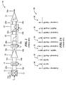
- a prior art magnetic field sensor 10 includes a Hall effect element 13 coupled within a switching circuit 12.
- the switching circuit 12 is configured to generate a differential output signal 12a, 12b responsive to an external magnetic field.
- Many signals described below can be differential signals, however, the term differential is not used in all instances. In other embodiments, some or all of the signals are single ended signals.
- the switching circuit 12 is more fully described below in conjunction with FIGS. 3-3C . Let it suffice here to say that the switching circuit 12 switches a drive signal (not shown) to the Hall effect element 12 with a clock at a frequency of f c
- the magnetic field sensor 10 also includes a switching circuit 14 coupled to receive the signal 12a, 12b and configured to generate a chopped signal 14a, 14b.
- the switching circuit 14 is also switched with the clock at a frequency of f c . Operation of the switching circuit 14 is also described more fully below in conjunction with FIGS. 3- 3C .
- An amplifier 16 is coupled to receive the chopped signal 14a, 14b and configured to generate an amplified signal 16a, 16b.
- a switching circuit 18 is coupled to receive the amplified signal 16a, 16b and configured to generate a demultiplexed signal 18a, 18b. The switching circuit 18 is clocked with the clock at the frequency, f c .
- a low pass filter 20 is coupled to receive the demultiplexed signal 18a, 18b and configured to generate a filtered signal 20a, 20b.
- a sinx/x (sinc) filter 22 is coupled to receive the filtered signal 20a, 20b and configured to generate a filtered signal 22a, 22b.
- a comparator 24, here a Schmitt trigger 24, is coupled to receive the filtered signal 22a, 22b and configured to generate a magnetic field sensor output signal 24a.
- the sinc filter 22 is a switched capacitor filter having a first notch at a frequency f c .
- the sinc filter 22 is generated digitally.
- the sinc filter 22 is an analog unclocked filter.
- clock frequency provided to the sinc filter 22 can be at a frequency of f c as shown to provide the notch at the frequency f c .
- the sinc filter 22 can be designed to have the notch at the frequency f c but using a clock signal at a different frequency.
- the clock provided to the sinc filter 22 is described to be at the frequency f c .
- the magnetic field sensor output signal 24a is a two state signal and that the magnetic field sensor 10 is a magnetic switch.
- the comparator 24 is replaced by a linear amplifier or buffer, and the magnetic field output signal is a linear signal. It will also be understood that, in some embodiments, only one of the filters 20, 22 is used.
- graphs 26 each include a horizontal axis having units of frequency in arbitrary units and a vertical axis having units of power in arbitrary units.
- a graph 28 is representative of the signal 12a, 12b, (i.e., frequency spectra of the signal 12a, 12b) and shows an external magnetic field signal, Bexternal, plus a residual offset signal, ResOff, appearing a frequency, which can be a zero frequency indicative of a DC external magnetic field.
- An external magnetic field signal, Bexternal plus a residual offset signal, ResOff, appearing a frequency, which can be a zero frequency indicative of a DC external magnetic field.
- a Hall effect offset signal, HallOff is at a different frequency, according to a frequency of the clock, f c . This effect is further described in conjunction with FIGS. 3-3C .
- the Hall effect offset signal, HallOff corresponds to a DC voltage error that would be present in the output signal 12, 12b of the Hall effect element 13, but when the switching circuit 12 is not switching, i.e., when the current through the Hall effect elements 104, 106 is directed in one particular respective direction.
- the Hall effect offset signal, HallOff is shifted to a higher frequency in the differential signal 12a, 12b by switching operation of the switching circuit 12 (and is shifted back to DC by operation of the switch circuit 14, as described below in conjunction with graph 30).
- the residual offset signal, ResOff corresponds to a remaining offset signal that remains at DC in the differential signal 12a, 12b even when the switching circuit 12 is switching (and is shifted to a higher frequency by operation of the switching circuit 14, as described below in conjunction with graph 30).
- a graph 30 is representative of the signal 14a, 14b, after chopping.
- the Hall offset signal, HallOff is shifted to DC by operation of the switching circuit 14, and the signal Bexternal + ResOff is at the frequency f c .
- a graph 32 is representative of the signal 16a, 16b.
- a DC offset of the amplifier 16 is added to the Hall offset signal at DC resulting in a signal HallOff + AmpOff at DC.
- a graph 34 is representative of the signal 18a, 18b, after the switching circuit 18. As can be seen, the signal Bexternal + ResOff is now at DC and the signal HallOff + AmpOff is now at the frequency, f c .
- a graph 36 is representative of the signals 20a, 20b after the filter 20.
- a break frequency of the filter 20 is selected to be below the frequency, f c .
- the signal HallOff + AmpOff is reduced, as is desired.
- a graph 38 is representative of the signal 22a, 22b, after the sinc filter 22.
- the notch of the sinc filter 22 is selected to be at the frequency, f c , i.e., at a Nyquist frequency of the sinc filter 22. Only the external magnetic field signal (plus some residual offset) remains in the graph 38 and in the signal 22a, 22b. The Hall effect element offset (HallOff) has been removed.
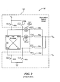
- a switched Hall element 50 of a type that modulates a Hall offset component includes a Hall element (or Hall plate) 52 and a modulation circuit 54.
- the Hall element 52 includes four contacts 52a, 52b, 52c, and 52d, each coupled to a first terminal of a respective switch 56a, 56b, 56c, and 56d, as shown.
- Second terminals of switches 56b and 56c are coupled to provide a positive node of a switched Hall output signal, here labeled Vo+, and second terminals of switches 56a and 56d are coupled to provide a negative node of the switched Hall output signal, here labeled Vo-.
- switches 60a, 60b, 60c, and 60d are arranged to selectively couple the Hall contacts 52a, 52b, 52c, 52d to the supply voltage, Vs, and ground. More particularly, switches 56b, 56d, 60a, and 60c are controlled by a clock signal, CLK, and switches 56a, 56c, 60b, and 60d are controlled by a complementary clock signal, CLK/, as shown.
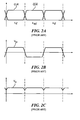
- the clock signals CLK and CLK/ have two states or phases, a ⁇ 0° state and a ⁇ 90° state, as shown in FIG. 2A .
- phase ⁇ 0° current flows from the terminal 52a to the terminal 52c and the switched Hall output signal, Vo, is equal to V H + V op , where V op is the Hall element offset voltage or Hall offset component and V H is the magnetic field signal component.
- the modulation circuit 54 modulates the Hall offset component, V op , which is shown in FIG. 2B for a zero Gauss magnetic field.
- the magnetic field signal component, V H remains substantially invariant, as shown in FIG. 2C .
- the chopping circuit 50 of FIG. 2 can be used as the switching circuits 12, 14 of FIG. 1 , however, the graphs 26 of FIG. 1 are representative of operation of the chopping circuit described below in conjunction with FIGS. 3-3C .
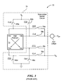
- an alternative switched Hall element 70 of a type that modulates a magnetic field signal component (which can be used for the switching circuits 12, 14 of FIG. 1 ) includes a Hall element 72 and a modulation circuit 74.
- the Hall effect element 72 is the same as the Hall effect element 52 of FIG. 2 and includes four contacts 72a, 72b, 72c, and 72d, each coupled to a first terminal of a respective switch 76a, 76b, 76c, and 76d.
- Second terminals of switches 76a and 76b are coupled to provide a positive node of a switched Hall output signal, here labeled Vo+, and second terminals of switches 56c and 56d are coupled to provide a negative node of the switched Hall output signal, here labeled Vo-.
- a comparison of FIGS. 2 and 3 reveals that the output contacts of the Hall element are interchanged during the ⁇ 90° phase.
- Additional switches 80a, 80b, 80c, and 80d are arranged to selectively couple the Hall contacts 72a, 72b, 72c, and 72d to the supply voltage Vs and ground.
- Switches 76b, 76d, 80a, and 80c are controlled by clock signal, CLK
- switches 76a, 76c, 80b, and 80d are controlled by a complementary clock signal, CLK/, as shown.
- Clock signals, CLK and CLK/ are identical to like signals in FIG. 2 and thus have two states or phases, ⁇ 0° and ⁇ 90° , as shown.
- phase ⁇ 0° current flows from the terminal 72a to the terminal 72c, and the switched Hall output signal, Vo, is equal to V H + V op .
- phase ⁇ 90° current flows from the terminal 72b to the terminal 72d, and the switched Hall output signal, Vo, is equal to -V H + V op .
- the modulation circuit 74 modulates the magnetic signal component to provide a modulated magnetic signal component, V H , which is shown in FIG. 3C for a zero Gauss magnetic field.
- the offset component, V op remains substantially invariant as is shown in FIG. 3B .
- switches 80a-80d can form a switching circuit the same as or similar to the switching circuit 12 of FIG. 1 . It will also be understood that the switches 76a-76d can form a switching circuit the same as or similar to the switching circuit 14 of FIG. 1
- the combination of the switching circuit 12 and the switching circuit 14 of FIG. 1 is of a type described above in conjunction with FIGS. 3-3C , rather than of a type described above in conjunction with FIGS. 2-2C .
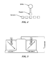
- a gear shifter can be disposed within an automobile. At the lower end of the gear shifter can be disposed a magnet. A plurality of magnetic field sensors can be disposed at positions to sense the position, and therefore, the selected gear, of the gear shifter.
- a failed magnetic field sensor can be reported to an operator of the automobile or to a mechanic by way of an indicator light or by way of a computer interface, for example an OBD-II computer interface, which is already present in automobiles sold in the U.S. since about 1996, but presently without such an indication of a failed magnetic field sensor associated with a gear shifter.
- two Hall effect elements can be coupled together in parallel.
- the two Hall effect elements coupled in parallel can be used in place of any of the single Hall effect elements described above in conjunction with FIGS. 1-3C .
- the output (plus an minus) of the two parallel Hall effect elements can be used in place of a plus and minus output from one Hall effect element.
- Drive signals (not shown in FIG. 5 ) can drive the two parallel Hall effect elements just as they drive the one Hall effect element in any of the above figures.
- the parallel arrangement of Hall effect elements is referred to herein as a normal mode configuration, as opposed to a diagnostic mode configuration described more fully below.
- the two Hall effect elements of FIG. 5 can be coupled together (i.e., re-connected) in a diagnostic mode configuration.
- the combination of the two Hall effect elements arranged in the diagnostic mode configuration is substantially unresponsive to an external magnetic field, Bexternal, in the same direction as experienced by each one of the two Hall effect elements.
- a residual response to the external magnetic field can be due to a mismatch of the two Hall effect elements, which would result in a residual external magnetic field signal.
- the two Hall effect elements are again shown arranged in the diagnostic mode configuration.
- two phases (directions) of each of the two diagnostic magnetic fields, Bcoil are shown.
- the output signal, V Bcoil is an AC signal.
- the output signal has substantially zero contribution from the external magnetic field, which is in the same direction at both Hall effect elements, regardless of whether the external magnetic field is a DC magnetic field or an AC magnetic field.
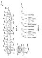
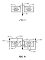
- magnetic field sensors of FIGS. 7 8 , 8B , 8D , and 8F are the same magnetic field sensor, but configured and operated in a normal mode of operation, a first version diagnostic mode of operation, a second version diagnostic mode of operation, a third version diagnostic mode of operation, and a fourth version diagnostic mode of operation, respectively. Accordingly, it will be recognized that circuit blocks of FIGS. 7 8 , 8B , 8D , and 8F are the same, but at least some of the signals within the figures are not the same.
- a magnetic field sensor 100 in a normal mode of operation, can be like the magnetic field sensor 10 of FIG. 1 , except that the magnetic field sensor 100 has two Hall effect elements 104,106 arranged in a normal mode configuration, the same as shown above in FIG. 5 .
- the magnetic field sensor includes a switching circuit 102 coupled to the two Hall effect elements 104, 106 and configured to generate a differential output signal 102a, 102b.
- a switching circuit 108 is coupled to receive the signal 102a, 102b and configured to generate an output signal 108a, 108b.
- the switching circuits 102 and 108 are more fully described below in conjunction with FIG. 17 .
- the switching circuit 102 is configured to configure the two Hall elements 104, 106 into the normal mode configuration of FIG. 5 , also to re-connect the two Hall effect elements 104, 106 into the diagnostic mode configuration of FIGS. 6 and 6A , and also configured, in some modes of operation, to switch a drive signal (not shown) to the Hall effect element 102, 104 with a clock at a frequency, resulting in a modulated (frequency shifted) signal.
- the drive signals to the two Hall effect elements 104, 106 are switched with a clock at a frequency of f c .
- the switching circuit 108 is representative of another modulation (or a demodulation) that can be generated by the same circuit as circuit 102 or by a different circuit.
- the switching circuit 108 is separately shown here for clarity.
- the switching circuit 102 can be the same as or similar to the switching circuit 12 of FIG. 1 .
- the switching circuit 102 allows for the two Hall effect elements 104, 106 to be connected into the normal mode configuration of FIG. 5 and re-connected into the diagnostic mode configuration of FIGS. 6, and 6A .
- Two coils 124, 126 and a switching circuit 122 are not used in the normal mode of operation of FIG. 7 , but are used in several forms of diagnostic mode of operation discussed below in conjunction with FIGS. 8-8G .
- signal 102a, 102b corresponds to the signal 12a, 12b
- signal 108a, 108b corresponds to the signal 14a
- 14b signal 110a, 110b corresponds to the signal 16a, 16b
- signal 112a, 112b corresponds to he signal 18a, 18b
- signal 114a, 114b corresponds to the signal 20a, 20b
- signal 116a, 116b corresponds to the signal 22a, 22b
- signal 118 corresponds to the signal 24a.
- Corresponding signals are essentially the same signals, except that in FIG. 7 , the signals originate from two Hall effect elements 104, 106 rather than from the one Hall effect element 13.
- FIG. 7A in which like elements of FIG. 1A are shown having like reference designations, in the normal mode configuration, all signals are the same as described above in conjunction with FIG. 1A .
- the graph 28 corresponds to the signal 102a, 102b
- the graph 30 corresponds to the signal 108a, 108b
- the graph 32 corresponds to the signal 110a, 110b
- the graph 34 corresponds to the signal 112a, 112b
- the graph 36 corresponds to the signal 114a, 114b
- the graph 38 corresponds to the signal 116a, 116b.
- a current, Icoil can be zero when in the normal mode configuration of FIG. 7 .
- the current, Icoil is generated and switched by the switching circuit 122, even when in the normal mode configuration of FIG. 7 .
- the output signal of the two Hall effect elements of FIGS. 5 and 7 is substantially zero.
- the current, Icoil is generated during both the normal mode of operation and during the diagnostic mode of operation described below.
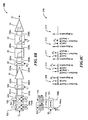
- a magnetic field sensor 150 is the same as or similar to the magnetic field sensor 100 of FIG. 7 , but is here shown with the two Hall effect elements 104, 106 re-connected into the diagnostic mode configuration described above in conjunction with FIGS. 6 and 6A .
- the switching circuit 102 can provide a re-connection of the Hall effect elements 104, 106 from the normal mode configuration of FIGS. 5 and 7 to the diagnostic mode configuration of FIGS. 6 and 6A .
- the magnetic field sensor 150 is provided to describe the first version diagnostic mode of operation.
- the magnetic field sensor 150 includes the two Hall effect elements 104, 106 coupled within the switching circuit 102.
- the switching circuit 102 is configured to generate a differential output signal 152a, 152b, which, unlike the signal 102a, 102b of FIG. 7 , is responsive to a diagnostic magnetic field generated by the two coils 124, 126 and not responsive to an external magnetic field.
- the switching circuit 102 is more fully described below in conjunction with FIG. 17 .
- Signals 152a, 152b, 154a, 154b, 156a, 156b, 158a, 158b, 160a, 160b, 162a, 162b, and 164 are different from the signals 102a, 102b, 104a, 104b, 106a, 106b, 108a, 108b, 110a, 110b, 112a, 112b, 114a, 114b, 116a, 116b, and 118 of FIG. 7 , since the Hall effect elements 104, 106 are differently coupled in FIG. 8 than in FIG. 7 , since the two Hall effect elements 104, 106 are responsive to diagnostic magnetic fields described more fully below and not responsive to the external magnetic field, and since the magnetic field sensor 150 operates in the fist version diagnostic mode of operation.
- the two diagnostic mode coils 124, 126 can be coupled to receive the current, Icoil, which, using a clock having a frequency of f c , is switched back and forth in direction by the switching circuit 122 coupled between the two diagnostic mode coils 124, 126 and the coil current, Icoil.
- the magnetic field sensor 150 is shown having a clocking arrangement indicative of the first version diagnostic mode of operation.
- the switching circuit 122 and the switching circuit 18 are clocked with a clock having a frequency of f c , and the sinc filter 22 has a notch at the frequency of f c .
- the switching circuit 108 is not switched at all and is fixed to a predetermined configuration, merely passing the signal 152a, 152b through the switching circuit 108.
- the switching circuit 102 is not switched, but merely provides the re-connection of the Hall effect elements from the normal mode configuration to the diagnostic mode configuration.
- the switching provided by the switching circuit 122 takes the place of the switching provided by the switching circuit 102 when in the normal mode of operation of FIG. 7 .
- the first version diagnostic mode of operation is able to perform a self-test of all of the parts of the magnetic field sensor 150, except for operation of the switching circuit 108.
- graphs 170 each include a horizontal axis having units of frequency in arbitrary units and a vertical axis having units of power in arbitrary units.
- a graph 172 is representative of the signal 152a, 152b, and also of the signal 154a, 154b, and shows the AC diagnostic magnetic field, Bdiagnostics, resulting from the two diagnostic coils 124, 126, appearing at a frequency, according to a frequency of the clock, f c , which clocks the switching circuit 122.
- a Hall effect element offset signal, HallOff summed with any residual signal due to the external magnetic field, ResBext, is at a different frequency, which can be zero.
- the signal, ResBext can result from a mismatch in the two Hall effect elements 104, 106 when coupled in the diagnostic mode configuration of FIGS. 6 and 6A .
- a graph 174 is representative of the signal 156a, 156b after the amplifier 16.
- the graph 174 is like the graph 172, except that an amplifier offset voltage, AmpOff, is added at DC.
- a graph 176 is representative of the signal 158a, 158b, after the switching circuit 18.
- the diagnostic magnetic field signal, Bdiagnostics is shifted to DC and the sum of the signals HallOff, ResBext, and AmpOff is now at the frequency, f c , which is the clocking frequency of the switching circuit 18.
- a graph 178 is representative of the signals 160a, 160b after the filter 20.
- a break frequency of the filter 20 is selected to be below the frequency, f c . The residual offsets and the amplifier offset are reduced.
- a graph 180 is representative of the signal 162a, 162b, after the sinc filter 22.
- the notch of the sinc filter 22 is selected to be at the frequency, f c . Only the diagnostic magnetic field signal remains in the graph 180 and in the signal 162a, 162b.
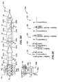
- a magnetic field sensor 200 is the same as or similar to the magnetic field sensors 100, 150 of FIGS. 7 and 8 .
- the two Hall effect elements 104, 106 are again re-connected, like in FIG. 8 , into the diagnostic mode configuration described above in conjunction with FIGS. 6, 6A , by operation of the switching circuit 102.
- the magnetic field sensor 200 is provided to describe the second version diagnostic mode of operation.
- the magnetic field sensor 200 includes the two Hall effect elements 104, 106 coupled within the switching circuit 102.
- the switching circuit 102 is configured to switch a drive signal to the Hall effect elements 104, 106 to generate a differential output signal 201a, 201 b, which, unlike the signal 102a, 102b of FIG. 7 , is responsive to a diagnostic magnetic field generated by the two coils 124, 126 and not responsive to an external magnetic field.
- the differential signal 201a, 201 b has different signal content due to different operation of the switching circuits 122, 102.
- the switching circuit 102 is more fully described below in conjunction with FIG. 17 .
- the switching circuit 102 is configured to re-connect the two Hall elements 104, 106 from the normal mode configuration of FIG. 5 to the diagnostic mode configuration of FIGS. 6 and 6A , but, unlike the magnetic field sensor 150 of FIG. 8 , the switching circuit 102 is configured to switch a drive signal (not shown) to the Hall effect elements 102, 104 using a clock with a frequency of f c .
- Signals 201a, 201b, 202a, 202b, 203a, 203b, 204a, 204b, 205a, 205b, 206a, 206b, and 207 are different from the signals 102a, 102b, 104a, 104b, 106a, 106b, 108a, 108b, 110a, 110b, 112a, 112b, 114a, 114b, 116a, 116b, and 118a of FIG.
- the two diagnostic mode coils 124, 126 can be coupled to receive the current, Icoil, which, using a clock having a frequency of 2f c , is switched back and forth in direction by the switching circuit 122 coupled between the two diagnostic mode coils 124, 126 and the coil current, Icoil.
- the magnetic field sensor 200 is shown having a clocking arrangement indicative of the second version diagnostic mode of operation.
- the switching circuit 122, and the switching circuit 18 are clocked with a clock having a frequency of 2f c
- the switching circuit 102 and the switching circuit 108 are clocked with a clock having a frequency of f c
- the sinc filter 22 has a notch at the frequency of f c .
- the second version diagnostic mode of operation is able to perform a self-test of all of the parts of the magnetic field sensor 200, including operation of the switching circuits 102, 108.
- graphs 208 each include a horizontal axis having units of frequency in arbitrary units and a vertical axis having units of power in arbitrary units.
- a graph 209 is representative of the differential signal 202a, 202b, and shows the AC diagnostic magnetic field, Bdiagnostics, resulting from the two diagnostic coils 124, 126, appearing at a frequency according to a frequency of the clock, 2f c , which clocks the switching circuit 122.
- the graph 209 also shows a spectral component corresponding to a Hall element offset voltage, HallOff, appearing at a frequency according to a frequency of the clock, f c , which clocks the switching circuit 102.
- a Hall effect element residual offset signal, ResOff summed with any residual signal due to the external magnetic field, ResBext, is at a different frequency, which can be zero.
- the signal, ResBext can result from a mismatch in the two Hall effect elements 104, 106 when coupled in the diagnostic mode configuration of FIGS. 6 and 6A .
- the switching circuit 108 does not operate to modulate the signal 201 a, 201b in the second version diagnostic mode of operation. In other words, the switching circuit 108 does not shift any signal frequencies. In essence, when the switching circuit 102 switches the drive signal to the two Hall effect elements, the output signal from the two Hall effect elements reverses polarity. The switching circuit 108 switches the two differential output signal 201a, 201b going into the amplifier 16, resulting in a positive signal always going into the same node (e.g., positive input node) of the amplifier 16 and a negative signal always going into the same node (e.g., negative input node) of the amplifier 16. Thus, no frequency shift results from operation of the switching circuit 108 in the second version diagnostic mode of operation.
- a graph 210 is representative of the signal 203a, 203b after the amplifier 16.
- the graph 210 is like the graph 209, except that an amplifier offset voltage, AmpOff, is added at DC.
- a graph 211 is representative of the signal 204a, 204b, after the switching circuit 18.
- the diagnostic magnetic field signal, Bdiagnostics is shifted to DC
- the sum of the signals ResBext, ResOff, and AmpOff is now at the frequency, 2f c
- the signal HallOff remains at the frequency, f c .
- a graph 212 is representative of the signal 205a, 205b after the filter 20.
- a break frequency of the filter 20 is selected to be below the frequency, f c .
- the residual offset signals, the amplifier offset signal, and the Hall element offset signal are reduced.
- a graph 213 is representative of the signal 206a, 206b, after the sinc filter 22.
- the notch of the sinc filter 22 is selected to be at the frequency, f c . Only the diagnostic magnetic field signal remains in the graph 213 and in the signal 206a, 206b.
- a magnetic field sensor 220 is the same as or similar to the magnetic field sensors 100, 150, 200 of FIGS. 7 , 8 , and 8B , respectively.
- the two Hall effect elements 104, 106 are again re-connected, like in FIGS. 8 and 8B , into the diagnostic mode configuration described above in conjunction with FIGS. 6, 6A by operation of the switching circuit 102.
- the magnetic field sensor 220 is provided to describe the third version diagnostic mode of operation.
- the magnetic field sensor 220 includes the two Hall effect elements 104, 106 coupled within the switching circuit 102.
- the switching circuit 102 is configured to switch a drive signal to the two Hall effect elements 104, 106 to generate a differential output signal 221a, 221b, which, unlike the signal 102a, 102b of FIG. 7 , is responsive to a diagnostic magnetic field generated by the two coils 124, 126 and not responsive to an external magnetic field.
- the signal 221a, 22 1 b has different signal content due to different operation of the switching circuits 122, 102.
- the switching circuit 102 is more fully described below in conjunction with FIG. 17 .
- the switching circuit 102 is configured to re-connect the two Hall elements 104, 106 from the normal mode configuration of FIG. 5 into the diagnostic mode configuration of FIGS. 6 and 6A , but, unlike the magnetic field sensor 150 of FIG. 8 , and unlike the magnetic field sensor 200 of FIG. 8B , the switching circuit 102 is configured to switch a drive signal (not shown) to the Hall effect elements 102, 104 using a clock with a frequency of 2f c .
- Signals 221a, 221b, 222a, 222b, 223a, 223b, 224a, 224b, 225a, 225b, 226a, 226b, and 227 are different from the signals 102a, 102b, 104a, 104b, 106a, 106b, 108a, 108b, 110a, 110b, 112a, 112b, 114a, 114b, 116a, 116b, and 118aofFIG.
- the two diagnostic mode coils 124, 126 can be coupled to receive the current, Icoil, which, using a clock having a frequency of f c , is switched back and forth in direction by the switching circuit 122 coupled between the two diagnostic mode coils 124, 126 and the coil current, Icoil.
- the magnetic field sensor 220 is shown having a clocking arrangement indicative of the third version diagnostic mode of operation.
- the switching circuit 122 and the switching circuit 18 are clocked with a clock having a frequency of f c
- the sinc filter 22 has a notch at the frequency of f c
- the switching circuit 102 and the switching circuit 108 are clocked with a clock having a frequency of 2f c .
- the third version diagnostic mode of operation is able to perform a self-test of all of the parts of the magnetic field sensor 220, including operation of the switching circuits 102, 108.
- graphs 228 each include a horizontal axis having units of frequency in arbitrary units and a vertical axis having units of power in arbitrary units.
- a graph 229 is representative of the signal 221a, 221 b, and shows the AC diagnostic magnetic field, Bdiagnostics, resulting from the two diagnostic coils 124, 126, appearing at a frequency according to a frequency of the clock, f c , which clocks the switching circuit 122.
- the graph 229 also shows a spectral component corresponding to a Hall element offset voltage, HallOff, appearing at a frequency according to a frequency of the clock, 2f c , which clocks the switching circuit 102.
- a Hall effect element residual offset signal, ResOff summed with any residual signal due to the external magnetic field, ResBext, is at a different frequency, which can be zero.
- the signal, ResBext can result from a mismatch in the two Hall effect elements 104, 106 when coupled in the diagnostic mode configuration of FIGS. 6 and 6A .
- the switching circuit 108 does not operate to modulate the signal 221a, 221b in the third version diagnostic mode of operation, for reasons described above in conjunction with FIG. 8C .
- a graph 230 is representative of the signal 223a, 223b after the amplifier 16.
- the graph 230 is like the graph 229, except that an amplifier offset voltage, AmpOff, is added at DC.
- a graph 231 is representative of the signal 224a, 224b, after the switching circuit 18.
- the diagnostic magnetic field signal, Bdiagnostics is shifted to DC
- the sum of the signals ResBext, ResOff, and AmpOff is now at the frequency, f c
- the signal HallOff remains at the frequency, f c .
- a specific phase of the signal controlling the switching circuit 18 is needed for the previous to occur.
- a graph 232 is representative of the signal 225a, 225b after the filter 20.
- a break frequency of the filter 20 is selected to be below the frequency, f c .
- the residual offset signals, the amplifier offset signal, and the Hall element offset signal are reduced.
- a graph 233 is representative of the signal 226a, 226b, after the sinc filter 22.
- the notch of the filter 22 is selected to be at the frequency, f c . Only the diagnostic magnetic field signal remains in the graph 233 and in the signal 226a, 226b.
- a magnetic field sensor 240 is the same as or similar to the magnetic field sensors 100, 150, 200, 220 of FIGS. 7 , 8 , 8B , and 8D , respectively.
- the two Hall effect elements 104, 106 are again re-connected, like in FIGS. 8 , 8B , and 8D , into the diagnostic mode configuration described above in conjunction with FIGS. 6, 6A by operation of the switching circuit 102.
- the magnetic field sensor 240 is provided to describe the fourth version diagnostic mode of operation.
- the magnetic field sensor 240 includes the two Hall effect elements 104, 106 coupled within the switching circuit 102.
- the switching circuit 102 is configured to switch a drive signal to the two Hall effect elements 104, 106 to generate a differential output signal 241 a, 241 b, which, unlike the signal 102a,102b of FIG. 7 , is responsive to a diagnostic magnetic field generated by the two coils 124, 126 and not responsive to an external magnetic field.
- the signal 221a, 221b has different signal content due to different operation of the switching circuits 122, 102.
- the switching circuit 102 is more fully described below in conjunction with FIG. 17 .
- the switching circuit 102 is configured to re-connect the two Hall elements 104, 106 from the normal mode configuration of FIG. 5 into the diagnostic mode configuration of FIGS. 6 and 6A , but, unlike the magnetic field sensor 150 of FIG. 8 , and unlike the magnetic field sensor 220 of FIG. 8D , the switching circuit 102 is configured to switch a drive signal (not shown) to the Hall effect elements 102, 104 using a clock with a frequency of f c .
- Signals 241a, 241b, 242a, 242b, 243a, 243b, 244a, 244b, 245a, 245b, 246a, 246b, and 247 are different from the signals 102a, 102b, 104a, 104b, 106a, 106b, 108a, 108b, 110a, 110b, 112a, 112b, 114a, 114b, 116a, 116b, and 118a of FIG.
- the two diagnostic mode coils 124, 126 can be coupled to receive the current, Icoil, which, using a clock having a frequency of f c /2, is switched back and forth in direction by the switching circuit 122 coupled between the two diagnostic mode coils 124, 126 and the coil current, Icoil.
- the magnetic field sensor 240 is shown having a clocking arrangement indicative of the fourth version diagnostic mode of operation.
- the switching circuit 122 and the switching circuit 18 are clocked with a clock having a frequency of f c /2
- the switching circuit 102 and the switching circuit 108 are clocked with a clock having a frequency of f c
- the sinc filter 22 has a notch at the frequency of f c /2, which can result from a clock signal to the sinc filter 22 having a frequency of f c or another frequency.
- the fourth version diagnostic mode of operation is able to perform a self-test of all of the parts of the magnetic field sensor 240, including operation of the switching circuits 102, 108.
- graphs 248 each include a horizontal axis having units of frequency in arbitrary units and a vertical axis having units of power in arbitrary units.
- a graph 249 is representative of the signal 241 a, 241b, and shows the AC diagnostic magnetic field, Bdiagnostics, resulting from the two diagnostic coils 124, 126, appearing at a frequency according to a frequency of the clock, f c /2, which clocks the switching circuit 122.
- the graph 249 also shows a spectral component corresponding to a Hall element offset voltage, HallOff, appearing at a frequency according to a frequency of the clock, f c , which clocks the switching circuit 102.
- a Hall effect element residual offset signal, ResOff summed with any residual signal due to the external magnetic field, ResBext, is at a different frequency, which can be zero.
- the signal, ResBext can result from a mismatch in the two Hall effect elements 104, 106 when coupled in the diagnostic mode configuration of FIGS. 6 and 6A .
- the switching circuit 108 operates to modulate the signal 221 a, 221 b in the fourth version diagnostic mode of operation.
- a graph 250 is representative of the signal 242a, 242b after the switching circuit 108.
- the graph 250 is like the graph 249, except that signal components, HallOff and ResBext+ResOff, are interchanged in frequency.
- a graph 251 is representative of the signal 243a, 243b after the amplifier 16.
- the graph 251 is like the graph 250, except that an amplifier offset voltage, AmpOff, is added at DC.
- a graph 252 is representative of the signal 244a, 244b, after the switching circuit 18.
- the diagnostic magnetic field signal, Bdiagnostics is shifted to DC
- the sum of the signals ResBext, ResOff is now at the frequency, f c /2
- the sum of the signals HallOff and AmpOff is also at the frequency, f c /2.
- a specific phase of the signal controlling the switching circuit 18 is needed for the previous to occur.
- a graph 253 is representative of the signal 245a, 245b after the filter 20.
- a break frequency of the filter 20 is selected to be below the frequency, f c .
- the residual offset signals, the amplifier offset signal, and the Hall element offset signal are reduced.
- a graph 254 is representative of the signal 246a, 246b, after the sinc filter 22.
- the notch of the filter 22 is selected to be at the frequency, f c . Only the diagnostic magnetic field signal remains in the graph 254 and in the signal 226a, 226b.
- harmonic content is omitted from the graphs of FIGS. 8A , 8C , 8E , and 8G for clarity.
- FIGS. 8 , 8B , 8D , and 8F corresponding to four exemplary version of the diagnostic mode of operation that show four exemplary relationships between clocks for the various circuit blocks.
- other clocks and other relative clock relationships can be used.
- phase chopping of the Hall effect element is shown to be provided by the above switching circuits 102, 108. However, in other embodiments, four phase or other phase chopping can be used.
- Circuits 16, 18, 20, 22, and 24 correspond to one form of a processing circuit configured to generate, during a first time period, a sensor output signal, e.g., 118) representative of the measured-magnetic-field-responsive signal portion, and configured to generate, during a second different time period, a sensor output signal (e.g., 164, 207, 227, 247) representative of the diagnostic-magnetic-field-responsive signal portion.
- the first time period corresponds to a time period during which the normal mode of operation is selected in accordance with FIG. 7 .
- the second different time period corresponds to a time period during which the diagnostic mode of operation is selected in accordance with FIGS 8-8G .
- FIGS. 9-9B are representations of the diagnostic coils 124, 126 of FIGS. 7 , 8 , 8B , and 8D above.
- the two diagnostic coils 124, 126 can be comprised of one conductor 260 running between the two Hall effect elements 104, 106. It will be appreciated that a current carried by the conductor 260 in a direction of the arrow tends to generate magnetic fields 260a into and out of the page, and in opposite directions at each of the two Hall effect elements 104, 106, as is desired when the two Hall effect elements 104, 106 are coupled in the diagnostic mode configuration of FIGS. 6 and 6A .
- the two diagnostic coils 124, 126 can be comprised of one conductor 262 running around and between the two Hall effect elements 104, 106.
- a current carried by the conductor 262 in a direction of the arrows tends to generate magnetic fields 262a, 262b, 262c into the page at the Hall effect element 104 and to generate magnetic fields 262d, 262e, 262f out of the page at the Hall effect element 106, i.e., in opposite directions at each of the two Hall effect elements 104, 106, as is desired when the two Hall effect elements 104, 106 are coupled in the diagnostic mode configuration of FIGS. 6 and 6A .
- the two diagnostic coils 124, 126 can be comprised of two coupled coils 264, 266 running around and between the two Hall effect elements 104, 106, and wound in opposite direction relative to the two Hall effect elements 104, 106. It will be appreciated that a current carried by the coil 264 in a direction of the arrow tends to generate a magnetic field into the page at the Hall effect element 104.
- a current carried by the coil 266 in a direction of the arrow tends to generate a magnetic field out of the page at the Hall effect element 106, i.e., in opposite directions at each of the two Hall effect elements 104, 106, as is desired when the two Hall effect elements 104, 106 are coupled in the diagnostic mode configuration of FIGS. 6 and 6A .
- magnetoresistance elements 284, 286 are shown in a series circuit 280, in a parallel circuit 300, and in an opposing circuit 320.
- the circuits 280 and 300 generate respective output signals 288a, 308a, which, like the normal mode configuration of Hall effect elements of FIG. 5 , are responsive to an external magnetic field, but not responsive to a diagnostic magnetic field experienced by the magnetoresistance elements 284, 286 in different directions.
- the circuit 320 generates an output signal 330a, which, like the diagnostic mode configuration of Hall effect elements of FIGS. 6 and 6A , is responsive to a diagnostic magnetic field experienced by the magnetoresistance elements 284, 286 in different directions, but not responsive to an external magnetic field.
- Hall effect elements 104, 106 of FIGS. 7 , 8 , 8B , 8D , and 8F can be replaced by magnetoresistance elements but with modifications to or removal of the switching circuits 102, 108.
- the coils 124, 126 can be comprised of a conductor 344 disposed on top of or underneath two magnetoresistance elements 340, 342. Magnetic fields 344a, 344b tend to be in opposite directions and parallel to surfaces of the magnetoresistance elements 340, 342.
- the two diagnostic coils 124, 126 of FIGS. 7 , 8 , 8B , 8D , and 8F can be comprised of coils 346, 348, each arranged to generate magnetic fields 346a, 348a in opposite directions parallel to a maximum response axis of the magnetoresistance elements 340, 342.
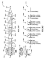
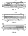
- FIGS. 12-12D show a variety of integrated circuit configurations. For clarity, only one magnetic field sensing element and one diagnostic coils (or conductor) are shown in the figures. However, one of ordinary skill in the art will understand how to fabricate an integrated circuit having two magnetic field sensing elements and two diagnostic coils. It will be appreciated that some of the magnetic field sensors of FIGS. 12-12D are shown to have electromagnetic shields. However, in other embodiments, the electromagnetic shields are omitted. Similarly, magnetic field sensors of FIGS. 12-12D shown without electromagnetic shields, can, in some other embodiments, have electromagnetic shields.
- a cross section of a portion of a magnetic field sensor 370 is representative of one of the two Hall effect elements 104, 106 and one of the diagnostic coils 124, 126 of FIGS. 7 , 8 , 8B , 8D , and 8F .
- the magnetic field sensor 370 includes a magnetic field sensing element 392 supported by a substrate 382 having a surface 382a.
- the magnetic field sensing element 392 may be impregnated into or diffused into and below the surface 382a of the substrate 382, such as is known for manufacturing of Hall effect elements.
- the magnetic field sensing element 392 can have a maximum response axis 396 generally perpendicular to the surface 382a of the substrate 382.
- the magnetic field sensor 370 can include metal layers 384, 386, 388 separated by insulating layers 376, 378, 380. Other metal and insulating layers (not shown) can be disposed between the insulating layer 376 and the metal layer 384.
- An electromagnetic shield 372 can be disposed over another insulating layer 374.
- Sections 394a-394c are representative of a diagnostic coil, such as one of the diagnostic coils 124, 126 of FIGS. 7 , 8 , 8B , 8D , and 8F .
- the sections 394a-394c can form one continuous self-test conductor, here disposed on different ones of the metal layers 384, 386, 388 and coupled by way of vias 390a, 390b.
- a self-test current carried by the self-test conductor 394a-394c tends to form a self-test magnetic field along the maximum response axis 396.
- a magnetic field sensor 400 can include all of the layers of the magnetic field sensor 370 of FIG. 12 and also the magnetic field sensing element 392 of FIG. 12 , but the self-test conductor 394a-394c of FIG. 12 can be replaced by a continuous external coil self-test conductor 402, which, in some embodiments, can be disposed upon a circuit board 404.
- the external self-test conductor 402 is representative of one of the diagnostic coils 124, 126 of FIGS. 7 , 8 , 8B , 8D , and 8F .
- the self-test conductor 402 shown on one metal layer of the circuit board 404, can instead be formed from a plurality of metal layers upon the circuit board 404.
- a self-test current carried by the self-test conductor 402 tends to form a self-test magnetic field along the maximum response axis 396.
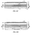
- a magnetic field sensor 410 can include all of the layers of the magnetic field sensors 370 of FIG. 12 and 400 of FIG. 12A , but the external self-test conductor 402 of FIG. 12A can be replaced by a continuous external coil self-test conductor 414. Furthermore, the magnetic field sensing element 392 of FIGS. 12 and 12A can be replaced by a magnetic field sensing element 412 having a maximum response axis 416 generally parallel to the surface 382a of the substrate 382 (e.g., a magnetoresistance element).
- the external self-test conductor 414 is representative of one of the diagnostic coils 124, 126 of FIGS. 7 , 8 , 8B , 8D , and 8F but for the magnetoresistance element arrangements of FIGS. 10-10B
- the magnetic field sensing element 412 may be disposed on or near the surface 382a of the substrate 382, such as is known for manufacturing of magnetoresistance elements.
- the magnetic field sensing element 392 can have a maximum response axis 416 generally parallel to the surface 382a of the substrate 382.
- a self-test current carried by the self-test conductor 414 tends to form a self-test magnetic field along the maximum response axis 416.
- a magnetic field sensor 420 can include all of the layers of the magnetic field sensors 370, 400 and 410 of FIGS. 12, 12A, and 12B , respectively, and also the magnetic field sensing element 412 of FIG. 12B , but the external self-test conductor 414 of FIG. 12B can be replaced by an internal single conductor self-test conductor 422 as is apparent from FIG. 11 .
- the self-test conductor 422 is representative of one of the diagnostic coils of FIGS. 7 , 8 , 8B , 8D , and 8F .
- a plurality of self test conductors can be used, which are arranged to provide a resulting magnetic field at the magnetic field sensing element 412 from the plurality of self test conductors generally aligned with the maximum response axis 416.
- a self-test current carried by the self-test conductor 422 tends to form a self-test magnetic field along the maximum response axis 416.
- a magnetic field sensor 430 can include all of the layers of the magnetic field sensors 370, 400, 410, and 420 of FIGS. 12, 12A, 12B , and 12C , respectively, but the internal self-test conductor 422 of FIG. 12C can be replaced by an external single conductor self-test conductor 432, which, in some embodiments, can be disposed upon a circuit board 434.
- the self-test conductor 432 is representative of one of the diagnostic coils of FIGS. 7 , 8 , 8B , 8D , and 8F .
- a plurality of self test conductors can be used, which are arranged to provide a resulting magnetic field at the magnetic field sensing element 412 from the plurality of self test conductors generally aligned with the maximum response axis 416.
- a self-test current carried by the self-test conductor 432 tends to form a self-test magnetic field along the maximum response axis 416.
- FIGS. 12-12D show various alternative embodiments associated with the magnetic field sensors of FIGS. 7 8 , 8B , 8D , and 8F , it will be recognized that there are many other possible configurations, including, but not limited to, combinations of the configurations shown.
- FIGS. 12-12D are representative of portions of magnetic field sensors 370, 400, 410, 420, 430, it should be understood that the magnetic field sensing elements and the self-test current conductors can be disposed on the same substrate as other portions of the magnetic field sensors of FIGS. 7 , 8 , 8B , 8D , and 8F , or, in other embodiments on a second different substrate from the other portions of the magnetic field sensors of FIGS. 7 , 8 , 8B , 8D , and 8F .
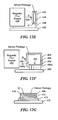
- a magnetic field sensor 444 here encased in a package 442, can be the same as or similar to the magnetic field sensors of FIGS. 7 , 8 , 8B , 8D , and 8F .
- the magnetic field sensor 444 can be coupled to a lead frame having leads 446.
- the leads 446 can be electrically coupled to a circuit board 450.
- the magnetic field sensor 444 can be responsive to a magnetic field 448 perpendicular to a major surface of the magnetic field sensor 444, such as may be generated by proximity of a magnetic field source 440, for example, a ferromagnetic object.
- a magnetic field sensor 456, here encased in a package 454, can be the same as or similar to the magnetic field sensors of FIGS. 7 , 8 , 8B , 8D , and 8F .
- the magnetic field sensor 456 can be coupled to a lead frame having leads, of which leads 460a, 460b are representative.
- the leads, e.g., 460a, 460b, can be electrically coupled to a circuit board 466.
- the magnetic field sensor 456 can be responsive to a magnetic field 464 parallel to a major surface of the magnetic field sensor 456, such as may be generated by proximity of a magnetic field (or flux) source 452, for example, a ferromagnetic object.
- the leads can be coupled with a measured conductor 458, which can be formed as a part of the lead frame of which the leads 460a, 460b are another part.
- a measured current carried by the measured conductor 458 tends to form a magnetic field 462 going into or out of the page, depending upon a direction of the current carried by the measured conductor 458.
- the magnetic field sensor 456 can be a current sensor and the magnetic field sensor 456 can instead be responsive to the magnetic field 462 perpendicular to the major surface of the magnetic field sensor 456 (i.e., to the current) rather than to the magnetic field 464.
- FIG. 12F While a particular integrated circuit package (e.g., a SIP) is shown in FIG. 12F , it should be understood that the same behavior can be accomplished with other integrated circuit packages, for example a-DIP, a-flip-chip, or an MLP package. With some of these packages, or with the SIP package if bent over, the magnetic field sensor 456 can be disposed having a major surface parallel to the circuit board 466.
- a SIP integrated circuit package
- a magnetic field sensor 470 here encased in a package 468, can be the same as or similar to the magnetic field sensors of FIGS. 7 , 8 , 8B , 8D , and 8F .
- the magnetic field sensor 470 can be coupled to a lead frame having leads, of which a lead 474 is representative.
- the leads, e.g., 474, can be electrically coupled to a circuit board 476.
- the magnetic field sensor 470 can be responsive to a magnetic field generated by proximity of a magnetic field source 472 within the package 468.
- the magnetic field source 472 can be a measured current conductor similar to the measured current conductor 458 of FIG. 12F .
- an exemplary electromagnetic shield 800 can be the same as or similar to the electromagnetic shield 372 of FIG. 12 .
- the electromagnetic shield 800 is placed generally over a magnetic field sensing element 816, which can be the same as or similar to the magnetic field sensing element 392 of FIG. 12 .
- the electromagnetic shield 800 includes a first portion 802 and a second portion 804 separated by a slit 806.
- the first portion 802 and the second portion 804 are coupled with a conductive region 808.
- a bonding pad 810 allows the electromagnetic shield 800 to be coupled to a DC voltage, for example, to a ground voltage.
- the electromagnetic shield 800 can be formed from a metal layer during manufacture of a magnetic field sensor, for example, the magnetic field sensors of FIGS. 7 , 8 , 8B , 8D , and 8F .
- the metal layer can be comprised of a variety of materials, for example, aluminum, copper, gold, titanium, tungsten, chromium, or nickel.
- a nickel layer would need to be thin so as not to concentrate the magnetic flux too much away from a Hall plate, especially if the shield has slits or slots.
- an electromagnetic shield is not the same as a magnetic shield.
- An electromagnetic shield is intended to block electromagnetic fields.
- a magnetic shield is intended to-block-magnetic fields.
- AC eddy currents 812, 814 can be induced in the electromagnetic shield 800.
- the eddy currents 812, 814 form into closed loops as shown.
- the closed loop eddy currents 812, 814 tend to result in a smaller magnetic field in proximity to the electromagnetic shield 800 than the magnetic field that induced the eddy currents 812, 814. Therefore, if the electromagnetic shield 800 were placed near a magnetic field sensing element, for example, the magnetic field sensing element 392 of FIG. 12 , the magnetic field sensing element 392 experiences a smaller magnetic field than it would otherwise experience, resulting in a less sensitive magnetic field sensor, which is generally undesirable. Furthermore, if the magnetic field associated with the eddy current is not uniform or symmetrical about the magnetic field sensing element 392, the magnetic field sensing element 392 might also generate an undesirable offset voltage.
- the slit 806 tends to reduce a size (i.e., a diameter or path length) of the closed loops in which the eddy currents 812, 814 travel. It will be understood that the reduced size of the closed loops in which the eddy currents 812, 814 travel results in smaller eddy currents 812, 814 and a smaller local effect on the AC magnetic field that induced the eddy current. Therefore, the sensitivity of a magnetic field sensor on which the magnetic field sensing element 816 and the electromagnetic shield 800 are used is less affected by the smaller eddy currents.
- the shield 800 in relation to the magnetic field sensing element 816 as shown, so that the slit 806 passes over the magnetic field sensing element 816, it will be understood that the magnetic field associated with any one of the eddy currents 812, 814 tends to form magnetic fields passing through the magnetic field sensing element 816 in two directions, canceling over at least a portion of the area of the magnetic field sensing element 816.
- another exemplary electromagnetic shield 850 can be the same as or similar to the electromagnetic shield 372 of FIG. 12 .
- the electromagnetic shield 850 includes four portions 852-858 separated by four slits 860-866.
- the four portions 852-858 are coupled with a conductive region 876.
- a bonding pad 878 allows the electromagnetic shield 850 to be coupled to a DC voltage, for example, a ground voltage.
- eddy currents 868-874 can be induced in the electromagnetic shield 850. Due to the four slits 860-866, it will be understood that a size (i.e., a diameter or a path length) of the closed loops eddy currents 866-874 tends to be smaller than the size of the closed loop eddy currents 812, 814 of FIG. 11 . It will be understood that the reduced size of the closed loops in which the eddy currents 868-874 travel results in smaller eddy currents 868-874 and a smaller local affect on the AC magnetic field that induced the eddy current than that which results from the shield 800 of FIG. 13 . Therefore, the sensitivity of a magnetic field sensor on which the magnetic field sensing element 880 and the electromagnetic shield 850 are used is less affected by the smaller eddy currents 868-874 than the sensitivity of a current sensor using the shield 800 of FIG. 13 .
- the shield 850 in relation to the magnetic field sensing element 880 as shown, so that the slits 860-866 pass over the magnetic field sensing element 880, it will be understood that the magnetic field associated with any one of the eddy currents 868-874, tends to form magnetic fields passing through the magnetic field sensing element 880 in two directions, canceling over at least a portion of the area of the magnetic field sensing element 880.
- the electromagnetic shield 900 includes a shielding portion 902 having interdigitated members, of which member 902a is but one example.
- the interdigitated members are coupled though a conductor portion 904 to a bonding pad 906, which allows the electromagnetic shield 900 to be coupled to a DC voltage, for example, a ground voltage.
- the electromagnetic shield 900 is able to support eddy currents having a much smaller size (i.e., diameter of path length) than the electromagnetic shield 850 of FIG. 14 or the electromagnetic shield 800 of FIG. 13 . Therefore, the electromagnetic shield 900 tends to have an even smaller negative affect on sensitivity of a magnetic field sensor than that described above.
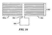
- an electromagnetic shield 950 can be the same as or similar to the electromagnetic shield 372 of FIG. 12 .
- the electromagnetic shield 950 includes a shielding portion 952 having a plurality of members, of which member 952a is but one example.
- the members are coupled though a conductor portion 954 to a bonding pad 956, which allows the electromagnetic shield 950 to be coupled to a DC voltage, for example, a ground voltage.
- a DC voltage for example, a ground voltage.
- the shield 372 of FIGS. 12, 12A , 12C, and 12D can also have no features to reduce eddy currents.
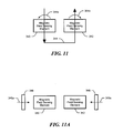
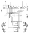
- switches S1-S8 can correspond to the switching circuit 102 of FIGS. 7 , 8 , 8B , 8D , and 8F .
- the switches S1-S4 can switch a direction of applied current to the two Hall effect elements 104, 106, to provide a first signal modulation comparable to that provided by the switches 60a-60d of FIG. 2 or 80a-80d of FIG. 3 .
- the switches S5-S8 perform two functions: to connect the Hall effect elements 104,106 into the normal mode or diagnostic mode of operation by selecting certain ones of the input nodes to each switch S5-S8, and also, in some embodiments, to modulate (or demodulate) the signal from the two Hall effect elements 104, 106 by switching between the certain ones of the input nodes to each switch S5-S8. Reconnection and switching of the switches S5-S8 is more fully described below in conjunction with FIG. 18 , and differs for each one of the four above-described diagnostic modes of operation.
- the connection into the normal mode or diagnostic mode of operation of the switches SS-S8 (as well as the operation of the switches S1-S4) is represented above within the switching circuit 102 of FIGS. 7 , 8 , 8B , 8D , and 8F .
- the modulation function of the switches S5-S8 is represented separately by the switching circuit 108 of FIGS. 7 , 8 , 8B , 8D , and 8F .
- the two switching circuits 102, 108 can be one switching circuit as shown in FIG. 17 .
- the two functions described above in conjunction with switches S5-S8 can be performed by two separate sets of switches.
- Circuit 1000 provides for the above-described normal mode configuration, the above-described four diagnostic mode configurations, and also allows for the clocking or non-clocking functions of the switching circuits 102, 108 described above, i.e., for normal mode of operation and for the first, second, third, and fourth version diagnostic modes of operation.
- a differential output signal, V+, V- is representative of an output signal from the switching circuit 108 of FIGS. 7 , 8 , 8B , 8D , or 8F , which output signal is different for each of the magnetic field sensors of FIGS. 7 , 8 , 8B , 8D , or 8F .
- the different output signals are determined according to switch positions and clocking of switches discussed below in conjunction with FIG. 18 .
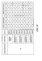
- FIG. 18 in which switches, S1-S8 of FIG. 17 are designated, a chart is representative of switch positions for the normal mode of operation and for the first, second, third, and fourth version diagnostic modes of operation.
- a column labeled "state" is representative of how the switches are changed during two phases of a clock signal, for the clock signals having relative frequencies described above in conjunction with FIGS. 7-8G .
- circuits show switch positions ( FIG. 17 ) and relative clock frequencies for the two phases (i.e., for the two drive directions provide by the switching circuit 102 of FIG. 7 , when operating in the normal mode of operation.
- circuits show switch positions ( FIG. 17 ) and relative clock frequencies for the two phases (i.e., for the two drive directions provide by the switching circuits 102 of FIG. 7 ) of the circuit 100 of FIG. 7 , operating generally in a diagnostic mode of operation.
- circuits show switch positions ( FIG. 17 ) and relative clock frequencies for the two phases (i.e., for the two drive directions provide by the switching circuits 102 of FIG. 8 ) of the circuit 150 of FIG. 8 , operating in the first version diagnostic mode of operation.
- circuits show switch positions ( FIG. 17 ) and relative clock frequencies for the two phases (i.e., for the two drive directions provide by the switching circuits 102 of FIG. 8B ) of the circuit 200 of FIG. 8B , operating in the second version diagnostic mode of operation.
- circuits show switch positions ( FIG. 17 ) and relative clock frequencies for the two phases (i.e., for the two drive directions provide by the switching circuits 102 of FIG. 8D ) of the circuit 220 of FIG. 8D , operating in the third version diagnostic mode of operation.
- circuits show switch positions ( FIG. 17 ) and relative clock frequencies for the two phases (i.e., for the two drive directions provide by the switching circuits 102 of FIG. 8F ) of the circuit 240 of FIG. 8F , operating in the fourth version diagnostic mode of operation.
Landscapes
- Physics & Mathematics (AREA)
- General Physics & Mathematics (AREA)
- Condensed Matter Physics & Semiconductors (AREA)
- Measuring Magnetic Variables (AREA)
- Hall/Mr Elements (AREA)
Priority Applications (1)
| Application Number | Priority Date | Filing Date | Title |
|---|---|---|---|
| EP13169661.9A EP2634592B1 (en) | 2009-07-22 | 2010-07-21 | Circuits and methods for generating a diagnostic mode of operation in a magnetic field sensor |
Applications Claiming Priority (2)
| Application Number | Priority Date | Filing Date | Title |
|---|---|---|---|
| US22762809P | 2009-07-22 | 2009-07-22 | |
| PCT/US2010/042694 WO2011011479A1 (en) | 2009-07-22 | 2010-07-21 | Circuits and methods for generating a diagnostic mode of operation in a magnetic field sensor |
Related Child Applications (2)
| Application Number | Title | Priority Date | Filing Date |
|---|---|---|---|
| EP13169661.9A Division EP2634592B1 (en) | 2009-07-22 | 2010-07-21 | Circuits and methods for generating a diagnostic mode of operation in a magnetic field sensor |
| EP13169661.9 Division-Into | 2013-05-29 |
Publications (2)
| Publication Number | Publication Date |
|---|---|
| EP2446287A1 EP2446287A1 (en) | 2012-05-02 |
| EP2446287B1 true EP2446287B1 (en) | 2013-10-02 |
Family
ID=42664764
Family Applications (2)
| Application Number | Title | Priority Date | Filing Date |
|---|---|---|---|
| EP10739429.8A Active EP2446287B1 (en) | 2009-07-22 | 2010-07-21 | Circuits and methods for generating a diagnostic mode of operation in a magnetic field sensor |
| EP13169661.9A Active EP2634592B1 (en) | 2009-07-22 | 2010-07-21 | Circuits and methods for generating a diagnostic mode of operation in a magnetic field sensor |
Family Applications After (1)
| Application Number | Title | Priority Date | Filing Date |
|---|---|---|---|
| EP13169661.9A Active EP2634592B1 (en) | 2009-07-22 | 2010-07-21 | Circuits and methods for generating a diagnostic mode of operation in a magnetic field sensor |
Country Status (5)
| Country | Link |
|---|---|
| US (2) | US8542010B2 (zh) |
| EP (2) | EP2446287B1 (zh) |
| JP (1) | JP5620989B2 (zh) |
| KR (1) | KR101673185B1 (zh) |
| WO (1) | WO2011011479A1 (zh) |
Cited By (1)
| Publication number | Priority date | Publication date | Assignee | Title |
|---|---|---|---|---|
| DE102015216262A1 (de) * | 2015-08-26 | 2017-03-02 | Fraunhofer-Gesellschaft zur Förderung der angewandten Forschung e.V. | Verfahren und Anordnung zur Bestimmung der Querempfindlichkeit von Magnetfeldsensoren |
Families Citing this family (130)
| Publication number | Priority date | Publication date | Assignee | Title |
|---|---|---|---|---|
| US9823090B2 (en) | 2014-10-31 | 2017-11-21 | Allegro Microsystems, Llc | Magnetic field sensor for sensing a movement of a target object |
| US8624588B2 (en) * | 2008-07-31 | 2014-01-07 | Allegro Microsystems, Llc | Apparatus and method for providing an output signal indicative of a speed of rotation and a direction of rotation as a ferromagnetic object |
| DE112010000848B4 (de) | 2009-02-17 | 2018-04-05 | Allegro Microsystems, Llc | Schaltungen und Verfahren zum Erzeugen eines Selbsttests eines Magnetfeldsensors |
| EP2446287B1 (en) | 2009-07-22 | 2013-10-02 | Allegro Microsystems, LLC | Circuits and methods for generating a diagnostic mode of operation in a magnetic field sensor |
| US8564285B2 (en) * | 2010-07-28 | 2013-10-22 | Allegro Microsystems, Llc | Magnetic field sensor with improved differentiation between a sensed magnetic field signal and a noise signal |
| US8947081B2 (en) | 2011-01-11 | 2015-02-03 | Invensense, Inc. | Micromachined resonant magnetic field sensors |
| US8860409B2 (en) * | 2011-01-11 | 2014-10-14 | Invensense, Inc. | Micromachined resonant magnetic field sensors |
| KR20120116036A (ko) * | 2011-04-12 | 2012-10-22 | 삼성전기주식회사 | 오프셋을 제거한 홀 센서 |
| US8680846B2 (en) * | 2011-04-27 | 2014-03-25 | Allegro Microsystems, Llc | Circuits and methods for self-calibrating or self-testing a magnetic field sensor |
| US8890518B2 (en) | 2011-06-08 | 2014-11-18 | Allegro Microsystems, Llc | Arrangements for self-testing a circular vertical hall (CVH) sensing element and/or for self-testing a magnetic field sensor that uses a circular vertical hall (CVH) sensing element |
| DE102011088365A1 (de) * | 2011-12-13 | 2013-06-13 | Zf Friedrichshafen Ag | Sensorvorrichtung, Verfahren zur Erfassung einer Position des Magnetelementes in Bezug zu einem Sensorelement und Magnetelement für eine Sensorvorrichtung |
| US9201122B2 (en) | 2012-02-16 | 2015-12-01 | Allegro Microsystems, Llc | Circuits and methods using adjustable feedback for self-calibrating or self-testing a magnetic field sensor with an adjustable time constant |
| US9817078B2 (en) | 2012-05-10 | 2017-11-14 | Allegro Microsystems Llc | Methods and apparatus for magnetic sensor having integrated coil |
| US8754640B2 (en) * | 2012-06-18 | 2014-06-17 | Allegro Microsystems, Llc | Magnetic field sensors and related techniques that can provide self-test information in a formatted output signal |
| US9068859B2 (en) | 2012-06-18 | 2015-06-30 | Allegro Microsystems, Llc | Magnetic field sensors and related techniques provide a self-test by communicating selected analog or digital samples of a proximity signal |
| US9222990B2 (en) | 2012-06-18 | 2015-12-29 | Allegro Microsystems, Llc | Magnetic field sensors and related techniques that can communicate at least one of three or more potential categories in which one or more characteristic values of a proximity signal responsive to a proximity of a sensed object are categorized |
| KR102055174B1 (ko) * | 2012-06-18 | 2019-12-12 | 알레그로 마이크로시스템스, 엘엘씨 | 감지된 물체의 근접에 반응하여 근접 신호의 하나 또는 그 이상의 특성 값들이 분류되는 셋 또는 그 이상의 포텐셜 카테고리들의 적어도 하나를 전달할 수 있는 자기장 센서들 및 관련 기술들 |
| US8860404B2 (en) | 2012-06-18 | 2014-10-14 | Allegro Microsystems, Llc | Magnetic field sensors and related techniques that can provide a self-test using signals and related thresholds |
| US9817083B2 (en) * | 2012-07-05 | 2017-11-14 | Allegro Microsystems, Llc | Magnetic field sensors and associated methods for removing undesirable spectral components |
| US8907669B2 (en) | 2012-07-24 | 2014-12-09 | Allegro Microsystems, Llc | Circuits and techniques for adjusting a sensitivity of a closed-loop current sensor |
| US9310446B2 (en) * | 2012-10-18 | 2016-04-12 | Analog Devices, Inc. | Magnetic field direction detector |
| US9354123B2 (en) * | 2012-12-26 | 2016-05-31 | Allegro Microsystems, Llc | Systems and methods for processing temperature data or other signals |
| US9383425B2 (en) | 2012-12-28 | 2016-07-05 | Allegro Microsystems, Llc | Methods and apparatus for a current sensor having fault detection and self test functionality |
| US10725100B2 (en) * | 2013-03-15 | 2020-07-28 | Allegro Microsystems, Llc | Methods and apparatus for magnetic sensor having an externally accessible coil |
| JP6212922B2 (ja) * | 2013-04-23 | 2017-10-18 | 株式会社リコー | チョッパ増幅装置 |
| US9664494B2 (en) * | 2013-05-10 | 2017-05-30 | Allegro Microsystems, Llc | Magnetic field sensor with immunity to external magnetic influences |
| JP6003816B2 (ja) * | 2013-06-10 | 2016-10-05 | 日立金属株式会社 | トルクセンサ |
| US9377327B2 (en) | 2013-06-28 | 2016-06-28 | Analog Devices Global | Magnetic field direction sensor |
| US9810519B2 (en) | 2013-07-19 | 2017-11-07 | Allegro Microsystems, Llc | Arrangements for magnetic field sensors that act as tooth detectors |
| US10145908B2 (en) * | 2013-07-19 | 2018-12-04 | Allegro Microsystems, Llc | Method and apparatus for magnetic sensor producing a changing magnetic field |
| US10495699B2 (en) | 2013-07-19 | 2019-12-03 | Allegro Microsystems, Llc | Methods and apparatus for magnetic sensor having an integrated coil or magnet to detect a non-ferromagnetic target |
| EP3203254A1 (en) | 2013-12-26 | 2017-08-09 | Allegro Microsystems, LLC | Methods and apparatus for sensor diagnostics |
| US9547048B2 (en) * | 2014-01-14 | 2017-01-17 | Allegro Micosystems, LLC | Circuit and method for reducing an offset component of a plurality of vertical hall elements arranged in a circle |
| US9791521B2 (en) * | 2014-03-27 | 2017-10-17 | Texas Instruments Incorporated | Systems and methods for operating a hall-effect sensor without an applied magnetic field |
| US9645220B2 (en) * | 2014-04-17 | 2017-05-09 | Allegro Microsystems, Llc | Circuits and methods for self-calibrating or self-testing a magnetic field sensor using phase discrimination |
| US9735773B2 (en) | 2014-04-29 | 2017-08-15 | Allegro Microsystems, Llc | Systems and methods for sensing current through a low-side field effect transistor |
| US9692329B2 (en) * | 2014-08-08 | 2017-06-27 | Johnson Electric S.A. | Magnetic sensor and an integrated circuit |
| US9716453B2 (en) | 2014-08-08 | 2017-07-25 | Johnson Electric S.A. | Magnetic sensor and an integrated circuit |
| US9696182B2 (en) * | 2014-08-08 | 2017-07-04 | Johnson Electric S.A. | Magnetic sensor and an integrated circuit |
| US9739846B2 (en) | 2014-10-03 | 2017-08-22 | Allegro Microsystems, Llc | Magnetic field sensors with self test |
| WO2016056179A1 (ja) | 2014-10-09 | 2016-04-14 | パナソニックIpマネジメント株式会社 | 磁気センサ |
| US9823092B2 (en) | 2014-10-31 | 2017-11-21 | Allegro Microsystems, Llc | Magnetic field sensor providing a movement detector |
| US9720054B2 (en) | 2014-10-31 | 2017-08-01 | Allegro Microsystems, Llc | Magnetic field sensor and electronic circuit that pass amplifier current through a magnetoresistance element |
| US10712403B2 (en) | 2014-10-31 | 2020-07-14 | Allegro Microsystems, Llc | Magnetic field sensor and electronic circuit that pass amplifier current through a magnetoresistance element |
| US9719806B2 (en) | 2014-10-31 | 2017-08-01 | Allegro Microsystems, Llc | Magnetic field sensor for sensing a movement of a ferromagnetic target object |
| US9804249B2 (en) | 2014-11-14 | 2017-10-31 | Allegro Microsystems, Llc | Dual-path analog to digital converter |
| US9804222B2 (en) | 2014-11-14 | 2017-10-31 | Allegro Microsystems, Llc | Magnetic field sensor with shared path amplifier and analog-to-digital-converter |
| US10466298B2 (en) | 2014-11-14 | 2019-11-05 | Allegro Microsystems, Llc | Magnetic field sensor with shared path amplifier and analog-to-digital-converter |
| US9841485B2 (en) | 2014-11-14 | 2017-12-12 | Allegro Microsystems, Llc | Magnetic field sensor having calibration circuitry and techniques |
| US9638764B2 (en) | 2015-04-08 | 2017-05-02 | Allegro Microsystems, Llc | Electronic circuit for driving a hall effect element with a current compensated for substrate stress |
| US11402440B2 (en) | 2015-07-17 | 2022-08-02 | Allegro Microsystems, Llc | Methods and apparatus for trimming a magnetic field sensor |
| US9551762B1 (en) | 2015-07-29 | 2017-01-24 | Allegro Microsystems, Llc | Circuits and methods for removing a gain offset in a magnetic field sensor |
| US9698742B2 (en) | 2015-10-06 | 2017-07-04 | Allegro Microsystems, Llc | Electronic amplifier with a feedback circuit that includes a transconductance amplifier |
| US10527703B2 (en) | 2015-12-16 | 2020-01-07 | Allegro Microsystems, Llc | Circuits and techniques for performing self-test diagnostics in a magnetic field sensor |
| FR3047318B1 (fr) * | 2016-01-29 | 2019-05-03 | Continental Automotive France | Procede et dispositif de test d'un capteur de detection pour vehicule automobile |
| US10495700B2 (en) | 2016-01-29 | 2019-12-03 | Allegro Microsystems, Llc | Method and system for providing information about a target object in a formatted output signal |
| US10107873B2 (en) | 2016-03-10 | 2018-10-23 | Allegro Microsystems, Llc | Electronic circuit for compensating a sensitivity drift of a hall effect element due to stress |
| WO2017163968A1 (ja) | 2016-03-22 | 2017-09-28 | パナソニックIpマネジメント株式会社 | 回転検出装置及びその補正方法 |
| JP6430565B2 (ja) | 2016-03-23 | 2018-11-28 | アナログ・デヴァイシズ・グローバル | 磁界検出器 |
| US10271467B2 (en) * | 2016-04-04 | 2019-04-23 | Prasad S. Joshi | Systems and methods for flux cancelation in electronic devices |
| CN107340483B (zh) * | 2016-04-29 | 2021-08-20 | 德昌电机(深圳)有限公司 | 一种磁传感器、磁传感器集成电路、电机组件及应用设备 |
| CN107332394B (zh) * | 2016-04-29 | 2020-08-04 | 德昌电机(深圳)有限公司 | 一种磁传感器、磁传感器集成电路、电机组件及应用设备 |
| DE102017108972A1 (de) * | 2016-04-29 | 2017-11-02 | Johnson Electric S.A. | Magnetsensor-Integrierte-Schaltung, Motoranordnung und Gebrauchsgerät |
| DE102017108974A1 (de) * | 2016-04-29 | 2017-11-02 | Johnson Electric S.A. | Magnetsensor-Integrierte-Schaltung, Motoranordnung und Gebrauchsgerät |
| EP4067908A1 (en) | 2016-05-17 | 2022-10-05 | Allegro MicroSystems, LLC | Magnetic field sensors and output signal formats for a magnetic field sensor |
| US10132879B2 (en) | 2016-05-23 | 2018-11-20 | Allegro Microsystems, Llc | Gain equalization for multiple axis magnetic field sensing |
| US10012518B2 (en) | 2016-06-08 | 2018-07-03 | Allegro Microsystems, Llc | Magnetic field sensor for sensing a proximity of an object |
| US10041810B2 (en) | 2016-06-08 | 2018-08-07 | Allegro Microsystems, Llc | Arrangements for magnetic field sensors that act as movement detectors |
| US10260905B2 (en) | 2016-06-08 | 2019-04-16 | Allegro Microsystems, Llc | Arrangements for magnetic field sensors to cancel offset variations |
| US10197638B2 (en) * | 2016-06-17 | 2019-02-05 | Texas Instruments Incorporated | High bandwidth hall sensor |
| US10162017B2 (en) | 2016-07-12 | 2018-12-25 | Allegro Microsystems, Llc | Systems and methods for reducing high order hall plate sensitivity temperature coefficients |
| DE112017003532T5 (de) | 2016-07-12 | 2019-04-04 | Panasonic Intellectual Property Management Co., Ltd. | Magnetsensor und Detektionsvorrichtung, die ihn verwendet |
| EP3293888B1 (en) | 2016-09-13 | 2020-08-26 | Allegro MicroSystems, LLC | Signal isolator having bidirectional communication between die |
| JP6853277B2 (ja) * | 2017-02-02 | 2021-03-31 | アルプスアルパイン株式会社 | 磁気平衡式電流センサおよびその製造方法 |
| US10761120B2 (en) | 2017-02-17 | 2020-09-01 | Allegro Microsystems, Llc | Current sensor system |
| US11428755B2 (en) | 2017-05-26 | 2022-08-30 | Allegro Microsystems, Llc | Coil actuated sensor with sensitivity detection |
| US10310028B2 (en) | 2017-05-26 | 2019-06-04 | Allegro Microsystems, Llc | Coil actuated pressure sensor |
| US10837943B2 (en) | 2017-05-26 | 2020-11-17 | Allegro Microsystems, Llc | Magnetic field sensor with error calculation |
| US10641842B2 (en) | 2017-05-26 | 2020-05-05 | Allegro Microsystems, Llc | Targets for coil actuated position sensors |
| US10996289B2 (en) | 2017-05-26 | 2021-05-04 | Allegro Microsystems, Llc | Coil actuated position sensor with reflected magnetic field |
| US10324141B2 (en) | 2017-05-26 | 2019-06-18 | Allegro Microsystems, Llc | Packages for coil actuated position sensors |
| JP6743770B2 (ja) * | 2017-06-16 | 2020-08-19 | 株式会社デンソー | ポジションセンサ |
| IT201700071213A1 (it) | 2017-06-26 | 2018-12-26 | St Microelectronics Srl | Circuito di lettura per sensori hall, dispositivo e procedimento corrispondenti |
| CN107305241B (zh) * | 2017-06-26 | 2021-01-29 | 新纳传感系统有限公司 | 一种磁传感装置及其实时自检方法 |
| US10739165B2 (en) | 2017-07-05 | 2020-08-11 | Analog Devices Global | Magnetic field sensor |
| US10520559B2 (en) | 2017-08-14 | 2019-12-31 | Allegro Microsystems, Llc | Arrangements for Hall effect elements and vertical epi resistors upon a substrate |
| US10481219B2 (en) | 2017-09-11 | 2019-11-19 | Allegro Microsystems, Llc | Magnetic field sensor with feedback loop for test signal processing |
| US10444299B2 (en) | 2017-09-11 | 2019-10-15 | Allegro Microsystems, Llc | Magnetic field sensor's front end and associated mixed signal method for removing chopper's related ripple |
| US10613158B2 (en) | 2017-10-12 | 2020-04-07 | Allegro Microsystems, Llc | Efficient signal path diagnostics for safety devices |
| US11249130B2 (en) * | 2017-12-29 | 2022-02-15 | Texas Instruments Incorporated | Direct current measurement of 1/f transistor noise |
| US10866117B2 (en) | 2018-03-01 | 2020-12-15 | Allegro Microsystems, Llc | Magnetic field influence during rotation movement of magnetic target |
| US10866289B2 (en) | 2018-03-27 | 2020-12-15 | Allegro Microsystems, Llc | Magnetic field sensor and associated methods including differential chopping |
| US10917092B2 (en) | 2018-04-06 | 2021-02-09 | Allegro Microsystems, Llc | Magnetic field sensor with switching network |
| US10955493B2 (en) | 2018-05-02 | 2021-03-23 | Analog Devices Global Unlimited Company | Magnetic sensor systems |
| US10656170B2 (en) | 2018-05-17 | 2020-05-19 | Allegro Microsystems, Llc | Magnetic field sensors and output signal formats for a magnetic field sensor |
| US10746814B2 (en) * | 2018-06-21 | 2020-08-18 | Allegro Microsystems, Llc | Diagnostic methods and apparatus for magnetic field sensors |
| US11255700B2 (en) | 2018-08-06 | 2022-02-22 | Allegro Microsystems, Llc | Magnetic field sensor |
| US10884031B2 (en) | 2018-08-17 | 2021-01-05 | Allegro Microsystems, Llc | Current sensor system |
| US11047887B2 (en) * | 2018-08-31 | 2021-06-29 | Asahi Kasei Microdevices Corporation | Current sensor, detection device, detection method, and program |
| US10823586B2 (en) | 2018-12-26 | 2020-11-03 | Allegro Microsystems, Llc | Magnetic field sensor having unequally spaced magnetic field sensing elements |
| US11061084B2 (en) | 2019-03-07 | 2021-07-13 | Allegro Microsystems, Llc | Coil actuated pressure sensor and deflectable substrate |
| US11047933B2 (en) | 2019-04-02 | 2021-06-29 | Allegro Microsystems, Llc | Fast response magnetic field sensors and associated methods for removing undesirable spectral components |
| US10955306B2 (en) | 2019-04-22 | 2021-03-23 | Allegro Microsystems, Llc | Coil actuated pressure sensor and deformable substrate |
| US11402280B2 (en) * | 2019-08-12 | 2022-08-02 | Allegro Microsystems, Llc | Magnetic sensor with improved stress compensation accounting for temperature |
| US11115244B2 (en) | 2019-09-17 | 2021-09-07 | Allegro Microsystems, Llc | Signal isolator with three state data transmission |
| US11280637B2 (en) | 2019-11-14 | 2022-03-22 | Allegro Microsystems, Llc | High performance magnetic angle sensor |
| US11237020B2 (en) | 2019-11-14 | 2022-02-01 | Allegro Microsystems, Llc | Magnetic field sensor having two rows of magnetic field sensing elements for measuring an angle of rotation of a magnet |
| US11194004B2 (en) | 2020-02-12 | 2021-12-07 | Allegro Microsystems, Llc | Diagnostic circuits and methods for sensor test circuits |
| US11169223B2 (en) | 2020-03-23 | 2021-11-09 | Allegro Microsystems, Llc | Hall element signal calibrating in angle sensor |
| US11226382B2 (en) | 2020-04-07 | 2022-01-18 | Allegro Microsystems, Llc | Current sensor system |
| DE102020110682A1 (de) * | 2020-04-20 | 2021-10-21 | Infineon Technologies Ag | Magnetfeldsensorvorrichtung und Verfahren |
| US11262422B2 (en) | 2020-05-08 | 2022-03-01 | Allegro Microsystems, Llc | Stray-field-immune coil-activated position sensor |
| US11519941B2 (en) | 2020-07-27 | 2022-12-06 | Analog Devices International Unlimited Company | Current sensing device having an integrated electrical shield |
| US11163019B1 (en) | 2020-08-05 | 2021-11-02 | Allegro Microsystems, Llc | Magnetic field sensors having stray field rejection |
| US11561257B2 (en) | 2020-12-22 | 2023-01-24 | Allegro Microsystems, Llc | Signal path monitor |
| US11555872B2 (en) | 2021-01-04 | 2023-01-17 | Allegro Microsystems, Llc | Reducing stray magnetic-field effects using a magnetic-field closed-loop system |
| US11927650B2 (en) | 2021-01-04 | 2024-03-12 | Allegro Microsystems, Llc | Magnetic-field closed-loop sensors with diagnostics |
| US11802922B2 (en) | 2021-01-13 | 2023-10-31 | Allegro Microsystems, Llc | Circuit for reducing an offset component of a plurality of vertical hall elements arranged in one or more circles |
| WO2022161631A1 (en) * | 2021-01-29 | 2022-08-04 | Advantest Corporation | An integrated circuit, an apparatus for testing an integrated circuit, a method for testing an integrated circuit and a computer program for implementing this method using magnetic field |
| US11493361B2 (en) | 2021-02-26 | 2022-11-08 | Allegro Microsystems, Llc | Stray field immune coil-activated sensor |
| US11630130B2 (en) | 2021-03-31 | 2023-04-18 | Allegro Microsystems, Llc | Channel sensitivity matching |
| US11567108B2 (en) | 2021-03-31 | 2023-01-31 | Allegro Microsystems, Llc | Multi-gain channels for multi-range sensor |
| US11578997B1 (en) | 2021-08-24 | 2023-02-14 | Allegro Microsystems, Llc | Angle sensor using eddy currents |
| US11656250B2 (en) | 2021-09-07 | 2023-05-23 | Allegro Microsystems, Llc | Current sensor system |
| US11782105B2 (en) | 2022-01-17 | 2023-10-10 | Allegro Microsystems, Llc | Fabricating planarized coil layer in contact with magnetoresistance element |
| US11630169B1 (en) | 2022-01-17 | 2023-04-18 | Allegro Microsystems, Llc | Fabricating a coil above and below a magnetoresistance element |
| US11892476B2 (en) | 2022-02-15 | 2024-02-06 | Allegro Microsystems, Llc | Current sensor package |
| US11994541B2 (en) | 2022-04-15 | 2024-05-28 | Allegro Microsystems, Llc | Current sensor assemblies for low currents |
| US11885866B2 (en) | 2022-05-31 | 2024-01-30 | Allegro Microsystems, Llc | Auto-calibration for coreless current sensors |
| US11940470B2 (en) | 2022-05-31 | 2024-03-26 | Allegro Microsystems, Llc | Current sensor system |
Family Cites Families (84)
| Publication number | Priority date | Publication date | Assignee | Title |
|---|---|---|---|---|
| DE2828605C3 (de) * | 1977-06-29 | 1982-01-14 | Tokyo Shibaura Denki K.K., Kawasaki, Kanagawa | Halbleitervorrichtung |
| DE3030620A1 (de) * | 1980-08-13 | 1982-03-11 | Siemens AG, 1000 Berlin und 8000 München | Anordnung zur aenderung der elektrischen schaltungskonfiguration von integrierten halbleiterschaltkreisen |
| CH664632A5 (de) * | 1984-08-16 | 1988-03-15 | Landis & Gyr Ag | Schaltungsanordnung zur kompensation von schwankungen des uebertragungsfaktors eines magnetfeldsensors. |
| SE447608B (sv) * | 1985-04-03 | 1986-11-24 | Hightech Network Ab | Forfarande och anordning for instellning av en digital regulator |
| US4833406A (en) * | 1986-04-17 | 1989-05-23 | Household Commercial Financial Services Inc. | Temperature compensated Hall-effect sensor apparatus |
| US4760285A (en) * | 1987-03-30 | 1988-07-26 | Honeywell Inc. | Hall effect device with epitaxal layer resistive means for providing temperature independent sensitivity |
| FR2614695B1 (fr) | 1987-04-28 | 1989-06-23 | Commissariat Energie Atomique | Procede de numerisation et de linearisation d'un capteur a caracteristique periodique quasi sinusoidale et dispositif correspondant |
| US4823075A (en) * | 1987-10-13 | 1989-04-18 | General Electric Company | Current sensor using hall-effect device with feedback |
| ATE86800T1 (de) * | 1988-04-21 | 1993-03-15 | Landis & Gyr Betriebs Ag | Integrierte halbleiterschaltung mit einem magnetfeldsensor aus halbleitermaterial. |
| EP0357013A3 (en) | 1988-09-02 | 1991-05-15 | Honeywell Inc. | Magnetic field measuring circuit |
| JPH03176682A (ja) * | 1989-12-06 | 1991-07-31 | Hitachi Ltd | 磁場計測装置 |
| JPH03248611A (ja) | 1990-02-27 | 1991-11-06 | Mitsubishi Electric Corp | 温度補償利得設定制御装置 |
| DE4114835A1 (de) * | 1991-05-07 | 1992-11-12 | Vdo Schindling | Schalteinrichtung, insbesondere zur verwendung in kraftfahrzeugen |
| US5247278A (en) * | 1991-11-26 | 1993-09-21 | Honeywell Inc. | Magnetic field sensing device |
| US5343143A (en) | 1992-02-11 | 1994-08-30 | Landis & Gyr Metering, Inc. | Shielded current sensing device for a watthour meter |
| US5469058A (en) * | 1992-12-30 | 1995-11-21 | Dunnam; Curt | Feedback enhanced sensor, alternating magnetic field detector |
| GB2276727B (en) | 1993-04-01 | 1997-04-09 | Rolls Royce & Ass | Improvements in and relating to magnetometers |
| US5424558A (en) * | 1993-05-17 | 1995-06-13 | High Yield Technology, Inc. | Apparatus and a method for dynamically tuning a particle sensor in response to varying process conditions |
| DE4319146C2 (de) * | 1993-06-09 | 1999-02-04 | Inst Mikrostrukturtechnologie | Magnetfeldsensor, aufgebaut aus einer Ummagnetisierungsleitung und einem oder mehreren magnetoresistiven Widerständen |
| US5329416A (en) | 1993-07-06 | 1994-07-12 | Alliedsignal Inc. | Active broadband magnetic flux rate feedback sensing arrangement |
| US6104231A (en) | 1994-07-19 | 2000-08-15 | Honeywell International Inc. | Temperature compensation circuit for a hall effect element |
| JPH08201490A (ja) * | 1995-01-31 | 1996-08-09 | Mitsumi Electric Co Ltd | センサic |
| DE19539458C2 (de) | 1995-10-24 | 2001-03-15 | Bosch Gmbh Robert | Sensor mit Testeingang |
| US5621319A (en) * | 1995-12-08 | 1997-04-15 | Allegro Microsystems, Inc. | Chopped hall sensor with synchronously chopped sample-and-hold circuit |
| DE19606826A1 (de) | 1996-02-23 | 1997-08-28 | Knorr Bremse Electronic Gmbh | Verfahren und Vorrichtung zur Überprüfung eines Sensors |
| US5844140A (en) | 1996-08-27 | 1998-12-01 | Seale; Joseph B. | Ultrasound beam alignment servo |
| US6011770A (en) * | 1997-12-10 | 2000-01-04 | Texas Instrumental Incorporated | Method and apparatus for high-order bandpass filter with linearly adjustable bandwidth |
| US6809515B1 (en) * | 1998-07-31 | 2004-10-26 | Spinix Corporation | Passive solid-state magnetic field sensors and applications therefor |
| US6351506B1 (en) * | 1999-04-19 | 2002-02-26 | National Semiconductor Corporation | Switched capacitor filter circuit having reduced offsets and providing offset compensation when used in a closed feedback loop |
| US6436748B1 (en) | 1999-08-31 | 2002-08-20 | Micron Technology, Inc. | Method for fabricating CMOS transistors having matching characteristics and apparatus formed thereby |
| FR2801445A1 (fr) * | 1999-11-23 | 2001-05-25 | Koninkl Philips Electronics Nv | Dispositif d'amplification a largeur de bande ajustable |
| US6917321B1 (en) * | 2000-05-21 | 2005-07-12 | Analog Devices, Inc. | Method and apparatus for use in switched capacitor systems |
| US6853178B2 (en) * | 2000-06-19 | 2005-02-08 | Texas Instruments Incorporated | Integrated circuit leadframes patterned for measuring the accurate amplitude of changing currents |
| DE10032530C2 (de) * | 2000-07-05 | 2002-10-24 | Infineon Technologies Ag | Verstärkerschaltung mit Offsetkompensation |
| US7190784B2 (en) * | 2000-12-29 | 2007-03-13 | Legerity, Inc. | Method and apparatus for adaptive DC level control |
| EP1260825A1 (de) * | 2001-05-25 | 2002-11-27 | Sentron Ag | Magnetfeldsensor |
| GB0126014D0 (en) * | 2001-10-30 | 2001-12-19 | Sensopad Technologies Ltd | Modulated field position sensor |
| US8107901B2 (en) * | 2001-08-20 | 2012-01-31 | Motorola Solutions, Inc. | Feedback loop with adjustable bandwidth |
| JP3877998B2 (ja) * | 2001-11-05 | 2007-02-07 | 株式会社山武 | 角度センサの温度情報検出装置および位置検出装置 |
| CN100443913C (zh) | 2002-11-13 | 2008-12-17 | 松下电器产业株式会社 | 磁场传感器和磁场检测装置及磁场检测方法 |
| JP2004177228A (ja) | 2002-11-26 | 2004-06-24 | Matsushita Electric Works Ltd | 電流計測装置 |
| US7259545B2 (en) | 2003-02-11 | 2007-08-21 | Allegro Microsystems, Inc. | Integrated sensor |
| US20060219436A1 (en) * | 2003-08-26 | 2006-10-05 | Taylor William P | Current sensor |
| JP2008504519A (ja) * | 2004-05-18 | 2008-02-14 | コーニンクレッカ フィリップス エレクトロニクス エヌ ヴィ | デジタル磁気電流センサおよびロジック |
| US7961823B2 (en) * | 2004-06-02 | 2011-06-14 | Broadcom Corporation | System and method for adjusting multiple control loops using common criteria |
| JP2006024845A (ja) | 2004-07-09 | 2006-01-26 | Yamaha Corp | プローブカード及び磁気センサの検査方法 |
| EP1637898A1 (en) | 2004-09-16 | 2006-03-22 | Liaisons Electroniques-Mecaniques Lem S.A. | Continuously calibrated magnetic field sensor |
| JP4440072B2 (ja) | 2004-10-26 | 2010-03-24 | パナソニック株式会社 | ロボットの制御方法 |
| JP2006126012A (ja) * | 2004-10-28 | 2006-05-18 | Asahi Kasei Microsystems Kk | 磁電変換システム及び磁電変換装置並びにその制御回路 |
| EP1679524A1 (en) | 2005-01-11 | 2006-07-12 | Ecole Polytechnique Federale De Lausanne Epfl - Sti - Imm - Lmis3 | Hall sensor and method of operating a Hall sensor |
| CN101116004B (zh) | 2005-02-08 | 2011-04-20 | 罗姆股份有限公司 | 磁传感器电路和具有该磁传感器电路的便携式终端 |
| DE102005047413B8 (de) | 2005-02-23 | 2012-05-10 | Infineon Technologies Ag | Magnetfeldsensorelement und Verfahren zum Durchführen eines On-Wafer-Funktionstests, sowie Verfahren zur Herstellung von Magnetfeldsensorelementen und Verfahren zur Herstellung von Magnetfeldsensorelementen mit On-Wafer-Funktionstest |
| US7325175B2 (en) * | 2005-05-04 | 2008-01-29 | Broadcom Corporation | Phase adjust using relative error |
| US7769110B2 (en) * | 2005-05-13 | 2010-08-03 | Broadcom Corporation | Threshold adjust system and method |
| US20070110199A1 (en) * | 2005-11-15 | 2007-05-17 | Afshin Momtaz | Receive equalizer with adaptive loops |
| US7292095B2 (en) * | 2006-01-26 | 2007-11-06 | Texas Instruments Incorporated | Notch filter for ripple reduction in chopper stabilized amplifiers |
| JP4916821B2 (ja) * | 2006-03-31 | 2012-04-18 | 株式会社ダイヘン | 電圧検出用プリント基板及びそれを用いた電圧検出器 |
| WO2007138508A1 (en) | 2006-05-30 | 2007-12-06 | Koninklijke Philips Electronics N. V. | Sensor device with adaptive field compensation |
| DE102006037226B4 (de) * | 2006-08-09 | 2008-05-29 | Fraunhofer-Gesellschaft zur Förderung der angewandten Forschung e.V. | Im Messbetrieb kalibrierbarer magnetischer 3D-Punktsensor |
| DE102006045141B9 (de) * | 2006-09-25 | 2009-02-19 | Infineon Technologies Ag | Magnetfeld-Sensor-Vorrichtung |
| GB0620307D0 (en) * | 2006-10-16 | 2006-11-22 | Ami Semiconductor Belgium Bvba | Auto-calibration of magnetic sensor |
| US7425821B2 (en) * | 2006-10-19 | 2008-09-16 | Allegro Microsystems, Inc. | Chopped Hall effect sensor |
| CN200986484Y (zh) | 2006-11-28 | 2007-12-05 | 李彩珍 | 磁场传感器 |
| US7729675B2 (en) * | 2006-12-08 | 2010-06-01 | Silicon Laboratories Inc. | Reducing noise during a gain change |
| US8128549B2 (en) * | 2007-02-20 | 2012-03-06 | Neuronetics, Inc. | Capacitor failure detection |
| JP5027217B2 (ja) * | 2007-03-23 | 2012-09-19 | 旭化成エレクトロニクス株式会社 | 磁気センサ及びその感度測定方法 |
| US7746675B2 (en) * | 2007-03-26 | 2010-06-29 | Virginia Tech Intellectual Properties, Inc. | Asymmetrical interleaving strategy for multi-channel power converters |
| US7982454B2 (en) * | 2007-06-26 | 2011-07-19 | Allegro Microsystems, Inc. | Calibration circuits and methods for a proximity detector using a first rotation detector for a determined time period and a second rotation detector after the determined time period |
| US7605580B2 (en) * | 2007-06-29 | 2009-10-20 | Infineon Technologies Austria Ag | Integrated hybrid current sensor |
| US7800389B2 (en) * | 2007-07-13 | 2010-09-21 | Allegro Microsystems, Inc. | Integrated circuit having built-in self-test features |
| US7694200B2 (en) * | 2007-07-18 | 2010-04-06 | Allegro Microsystems, Inc. | Integrated circuit having built-in self-test features |
| DE102007041230B3 (de) | 2007-08-31 | 2009-04-09 | Fraunhofer-Gesellschaft zur Förderung der angewandten Forschung e.V. | Kalibrierbarer mehrdimensionaler magnetischer Punktsensor sowie entsprechendes Verfahren und Computerprogramm dafür |
| US7973635B2 (en) * | 2007-09-28 | 2011-07-05 | Access Business Group International Llc | Printed circuit board coil |
| US7923996B2 (en) * | 2008-02-26 | 2011-04-12 | Allegro Microsystems, Inc. | Magnetic field sensor with automatic sensitivity adjustment |
| US7936144B2 (en) * | 2008-03-06 | 2011-05-03 | Allegro Microsystems, Inc. | Self-calibration algorithms in a small motor driver IC with an integrated position sensor |
| US7605647B1 (en) * | 2008-04-29 | 2009-10-20 | Allegro Microsystems, Inc. | Chopper-stabilized amplifier and magnetic field sensor |
| US7764118B2 (en) * | 2008-09-11 | 2010-07-27 | Analog Devices, Inc. | Auto-correction feedback loop for offset and ripple suppression in a chopper-stabilized amplifier |
| DE112010000848B4 (de) * | 2009-02-17 | 2018-04-05 | Allegro Microsystems, Llc | Schaltungen und Verfahren zum Erzeugen eines Selbsttests eines Magnetfeldsensors |
| US7990209B2 (en) * | 2009-06-19 | 2011-08-02 | Allegro Microsystems, Inc. | Switched capacitor notch filter |
| EP2446287B1 (en) | 2009-07-22 | 2013-10-02 | Allegro Microsystems, LLC | Circuits and methods for generating a diagnostic mode of operation in a magnetic field sensor |
| US8299783B2 (en) * | 2009-08-27 | 2012-10-30 | Allegro Microsystems, Inc. | Circuits and methods for calibration of a motion detector |
| JP2011052036A (ja) | 2009-08-31 | 2011-03-17 | Nippon Synthetic Chem Ind Co Ltd:The | エポキシ樹脂用硬化剤 |
| US8680848B2 (en) * | 2010-06-03 | 2014-03-25 | Allegro Microsystems, Llc | Motion sensor, method, and computer-readable storage medium providing a motion sensor that adjusts gains of two circuit channels to bring the gains close to each other |
| EP2402777B1 (en) * | 2010-06-30 | 2013-01-09 | LEM Intellectual Property SA | Autonomously calibrated magnetic field sensor |
-
2010
- 2010-07-21 EP EP10739429.8A patent/EP2446287B1/en active Active
- 2010-07-21 EP EP13169661.9A patent/EP2634592B1/en active Active
- 2010-07-21 WO PCT/US2010/042694 patent/WO2011011479A1/en active Application Filing
- 2010-07-21 JP JP2012521746A patent/JP5620989B2/ja active Active
- 2010-07-21 US US12/840,324 patent/US8542010B2/en active Active
- 2010-07-21 KR KR1020127004427A patent/KR101673185B1/ko active IP Right Grant
-
2013
- 2013-08-19 US US13/969,702 patent/US8692546B2/en active Active
Cited By (2)
| Publication number | Priority date | Publication date | Assignee | Title |
|---|---|---|---|---|
| DE102015216262A1 (de) * | 2015-08-26 | 2017-03-02 | Fraunhofer-Gesellschaft zur Förderung der angewandten Forschung e.V. | Verfahren und Anordnung zur Bestimmung der Querempfindlichkeit von Magnetfeldsensoren |
| DE102015216262B4 (de) * | 2015-08-26 | 2019-03-28 | Fraunhofer-Gesellschaft zur Förderung der angewandten Forschung e.V. | Verfahren und Anordnung zur Bestimmung der Querempfindlichkeit von Magnetfeldsensoren |
Also Published As
| Publication number | Publication date |
|---|---|
| KR20120040247A (ko) | 2012-04-26 |
| US8692546B2 (en) | 2014-04-08 |
| US20130335066A1 (en) | 2013-12-19 |
| KR101673185B1 (ko) | 2016-11-07 |
| US8542010B2 (en) | 2013-09-24 |
| JP5620989B2 (ja) | 2014-11-05 |
| US20110018533A1 (en) | 2011-01-27 |
| JP2013500469A (ja) | 2013-01-07 |
| EP2634592B1 (en) | 2015-01-14 |
| EP2634592A1 (en) | 2013-09-04 |
| WO2011011479A1 (en) | 2011-01-27 |
| EP2446287A1 (en) | 2012-05-02 |
Similar Documents
| Publication | Publication Date | Title |
|---|---|---|
| EP2446287B1 (en) | Circuits and methods for generating a diagnostic mode of operation in a magnetic field sensor | |
| EP3123188B1 (en) | Circuits and methods for self-calibrating or self-testing a magnetic field sensor using phase discrimination | |
| US8680846B2 (en) | Circuits and methods for self-calibrating or self-testing a magnetic field sensor | |
| US9551762B1 (en) | Circuits and methods for removing a gain offset in a magnetic field sensor | |
| US9958482B1 (en) | Systems and methods for a high isolation current sensor | |
| US11112467B2 (en) | Magnetic field sensor circuit in package with means to add a signal from a coil | |
| US11397225B2 (en) | Current sensor, magnetic sensor and circuit | |
| WO2007010378A1 (en) | Orthogonal fluxgate magnetic field sensor | |
| KR20130049759A (ko) | 단일 자기저항 센서를 이용한 자기장의 평면내 자기장 성분 결정 장치 및 방법 | |
| KR20130049741A (ko) | 약한 자기장을 감지하는 2차 고조파 검출 모드에서 자기저항 센서를 사용하는 방법 | |
| US11561112B2 (en) | Current sensor having stray field immunity | |
| JP2010281821A (ja) | 磁界補償 | |
| JP2022548498A (ja) | 差動信号電流センサ | |
| JP2019219294A (ja) | 磁気センサ | |
| JP2010286270A (ja) | 電流センサ | |
| US20220373617A1 (en) | Sensor device with sensor and current converter | |
| JP2019002688A (ja) | 勾配磁界センサ |
Legal Events
| Date | Code | Title | Description |
|---|---|---|---|
| PUAI | Public reference made under article 153(3) epc to a published international application that has entered the european phase |
Free format text: ORIGINAL CODE: 0009012 |
|
| 17P | Request for examination filed |
Effective date: 20120127 |
|
| AK | Designated contracting states |
Kind code of ref document: A1 Designated state(s): AL AT BE BG CH CY CZ DE DK EE ES FI FR GB GR HR HU IE IS IT LI LT LU LV MC MK MT NL NO PL PT RO SE SI SK SM TR |
|
| DAX | Request for extension of the european patent (deleted) | ||
| GRAP | Despatch of communication of intention to grant a patent |
Free format text: ORIGINAL CODE: EPIDOSNIGR1 |
|
| GRAP | Despatch of communication of intention to grant a patent |
Free format text: ORIGINAL CODE: EPIDOSNIGR1 |
|
| INTG | Intention to grant announced |
Effective date: 20130417 |
|
| RAP1 | Party data changed (applicant data changed or rights of an application transferred) |
Owner name: ALLEGRO MICROSYSTEMS, LLC |
|
| GRAS | Grant fee paid |
Free format text: ORIGINAL CODE: EPIDOSNIGR3 |
|
| GRAA | (expected) grant |
Free format text: ORIGINAL CODE: 0009210 |
|
| AK | Designated contracting states |
Kind code of ref document: B1 Designated state(s): AL AT BE BG CH CY CZ DE DK EE ES FI FR GB GR HR HU IE IS IT LI LT LU LV MC MK MT NL NO PL PT RO SE SI SK SM TR |
|
| REG | Reference to a national code |
Ref country code: GB Ref legal event code: FG4D |
|
| REG | Reference to a national code |
Ref country code: CH Ref legal event code: EP Ref country code: AT Ref legal event code: REF Ref document number: 634858 Country of ref document: AT Kind code of ref document: T Effective date: 20131015 |
|
| REG | Reference to a national code |
Ref country code: IE Ref legal event code: FG4D |
|
| REG | Reference to a national code |
Ref country code: DE Ref legal event code: R096 Ref document number: 602010010700 Country of ref document: DE Effective date: 20131205 |
|
| REG | Reference to a national code |
Ref country code: NL Ref legal event code: VDEP Effective date: 20131002 |
|
| PG25 | Lapsed in a contracting state [announced via postgrant information from national office to epo] |
Ref country code: SI Free format text: LAPSE BECAUSE OF FAILURE TO SUBMIT A TRANSLATION OF THE DESCRIPTION OR TO PAY THE FEE WITHIN THE PRESCRIBED TIME-LIMIT Effective date: 20131002 |
|
| REG | Reference to a national code |
Ref country code: LT Ref legal event code: MG4D |
|
| PG25 | Lapsed in a contracting state [announced via postgrant information from national office to epo] |
Ref country code: IS Free format text: LAPSE BECAUSE OF FAILURE TO SUBMIT A TRANSLATION OF THE DESCRIPTION OR TO PAY THE FEE WITHIN THE PRESCRIBED TIME-LIMIT Effective date: 20140202 Ref country code: HR Free format text: LAPSE BECAUSE OF FAILURE TO SUBMIT A TRANSLATION OF THE DESCRIPTION OR TO PAY THE FEE WITHIN THE PRESCRIBED TIME-LIMIT Effective date: 20131002 Ref country code: NL Free format text: LAPSE BECAUSE OF FAILURE TO SUBMIT A TRANSLATION OF THE DESCRIPTION OR TO PAY THE FEE WITHIN THE PRESCRIBED TIME-LIMIT Effective date: 20131002 Ref country code: LT Free format text: LAPSE BECAUSE OF FAILURE TO SUBMIT A TRANSLATION OF THE DESCRIPTION OR TO PAY THE FEE WITHIN THE PRESCRIBED TIME-LIMIT Effective date: 20131002 Ref country code: SE Free format text: LAPSE BECAUSE OF FAILURE TO SUBMIT A TRANSLATION OF THE DESCRIPTION OR TO PAY THE FEE WITHIN THE PRESCRIBED TIME-LIMIT Effective date: 20131002 Ref country code: FI Free format text: LAPSE BECAUSE OF FAILURE TO SUBMIT A TRANSLATION OF THE DESCRIPTION OR TO PAY THE FEE WITHIN THE PRESCRIBED TIME-LIMIT Effective date: 20131002 Ref country code: NO Free format text: LAPSE BECAUSE OF FAILURE TO SUBMIT A TRANSLATION OF THE DESCRIPTION OR TO PAY THE FEE WITHIN THE PRESCRIBED TIME-LIMIT Effective date: 20140102 Ref country code: CZ Free format text: LAPSE BECAUSE OF FAILURE TO SUBMIT A TRANSLATION OF THE DESCRIPTION OR TO PAY THE FEE WITHIN THE PRESCRIBED TIME-LIMIT Effective date: 20131002 |
|
| PG25 | Lapsed in a contracting state [announced via postgrant information from national office to epo] |
Ref country code: PL Free format text: LAPSE BECAUSE OF FAILURE TO SUBMIT A TRANSLATION OF THE DESCRIPTION OR TO PAY THE FEE WITHIN THE PRESCRIBED TIME-LIMIT Effective date: 20131002 Ref country code: ES Free format text: LAPSE BECAUSE OF FAILURE TO SUBMIT A TRANSLATION OF THE DESCRIPTION OR TO PAY THE FEE WITHIN THE PRESCRIBED TIME-LIMIT Effective date: 20131002 Ref country code: LV Free format text: LAPSE BECAUSE OF FAILURE TO SUBMIT A TRANSLATION OF THE DESCRIPTION OR TO PAY THE FEE WITHIN THE PRESCRIBED TIME-LIMIT Effective date: 20131002 Ref country code: CY Free format text: LAPSE BECAUSE OF FAILURE TO SUBMIT A TRANSLATION OF THE DESCRIPTION OR TO PAY THE FEE WITHIN THE PRESCRIBED TIME-LIMIT Effective date: 20131002 |
|
| PG25 | Lapsed in a contracting state [announced via postgrant information from national office to epo] |
Ref country code: PT Free format text: LAPSE BECAUSE OF FAILURE TO SUBMIT A TRANSLATION OF THE DESCRIPTION OR TO PAY THE FEE WITHIN THE PRESCRIBED TIME-LIMIT Effective date: 20140203 |
|
| REG | Reference to a national code |
Ref country code: DE Ref legal event code: R097 Ref document number: 602010010700 Country of ref document: DE |
|
| PG25 | Lapsed in a contracting state [announced via postgrant information from national office to epo] |
Ref country code: EE Free format text: LAPSE BECAUSE OF FAILURE TO SUBMIT A TRANSLATION OF THE DESCRIPTION OR TO PAY THE FEE WITHIN THE PRESCRIBED TIME-LIMIT Effective date: 20131002 |
|
| PLBE | No opposition filed within time limit |
Free format text: ORIGINAL CODE: 0009261 |
|
| STAA | Information on the status of an ep patent application or granted ep patent |
Free format text: STATUS: NO OPPOSITION FILED WITHIN TIME LIMIT |
|
| PG25 | Lapsed in a contracting state [announced via postgrant information from national office to epo] |
Ref country code: SK Free format text: LAPSE BECAUSE OF FAILURE TO SUBMIT A TRANSLATION OF THE DESCRIPTION OR TO PAY THE FEE WITHIN THE PRESCRIBED TIME-LIMIT Effective date: 20131002 Ref country code: IT Free format text: LAPSE BECAUSE OF FAILURE TO SUBMIT A TRANSLATION OF THE DESCRIPTION OR TO PAY THE FEE WITHIN THE PRESCRIBED TIME-LIMIT Effective date: 20131002 Ref country code: RO Free format text: LAPSE BECAUSE OF FAILURE TO SUBMIT A TRANSLATION OF THE DESCRIPTION OR TO PAY THE FEE WITHIN THE PRESCRIBED TIME-LIMIT Effective date: 20131002 |
|
| 26N | No opposition filed |
Effective date: 20140703 |
|
| PG25 | Lapsed in a contracting state [announced via postgrant information from national office to epo] |
Ref country code: DK Free format text: LAPSE BECAUSE OF FAILURE TO SUBMIT A TRANSLATION OF THE DESCRIPTION OR TO PAY THE FEE WITHIN THE PRESCRIBED TIME-LIMIT Effective date: 20131002 |
|
| REG | Reference to a national code |
Ref country code: DE Ref legal event code: R097 Ref document number: 602010010700 Country of ref document: DE Effective date: 20140703 |
|
| PG25 | Lapsed in a contracting state [announced via postgrant information from national office to epo] |
Ref country code: LU Free format text: LAPSE BECAUSE OF FAILURE TO SUBMIT A TRANSLATION OF THE DESCRIPTION OR TO PAY THE FEE WITHIN THE PRESCRIBED TIME-LIMIT Effective date: 20140721 |
|
| REG | Reference to a national code |
Ref country code: CH Ref legal event code: PL |
|
| REG | Reference to a national code |
Ref country code: DE Ref legal event code: R082 Ref document number: 602010010700 Country of ref document: DE Representative=s name: LIPPERT STACHOW PATENTANWAELTE RECHTSANWAELTE , DE Ref country code: DE Ref legal event code: R082 Ref document number: 602010010700 Country of ref document: DE Representative=s name: PATENTANWAELTE LIPPERT, STACHOW & PARTNER, DE |
|
| GBPC | Gb: european patent ceased through non-payment of renewal fee |
Effective date: 20140721 |
|
| REG | Reference to a national code |
Ref country code: IE Ref legal event code: MM4A |
|
| PG25 | Lapsed in a contracting state [announced via postgrant information from national office to epo] |
Ref country code: CH Free format text: LAPSE BECAUSE OF NON-PAYMENT OF DUE FEES Effective date: 20140731 Ref country code: LI Free format text: LAPSE BECAUSE OF NON-PAYMENT OF DUE FEES Effective date: 20140731 |
|
| PG25 | Lapsed in a contracting state [announced via postgrant information from national office to epo] |
Ref country code: GB Free format text: LAPSE BECAUSE OF NON-PAYMENT OF DUE FEES Effective date: 20140721 |
|
| PG25 | Lapsed in a contracting state [announced via postgrant information from national office to epo] |
Ref country code: IE Free format text: LAPSE BECAUSE OF NON-PAYMENT OF DUE FEES Effective date: 20140721 |
|
| PG25 | Lapsed in a contracting state [announced via postgrant information from national office to epo] |
Ref country code: MC Free format text: LAPSE BECAUSE OF FAILURE TO SUBMIT A TRANSLATION OF THE DESCRIPTION OR TO PAY THE FEE WITHIN THE PRESCRIBED TIME-LIMIT Effective date: 20131002 Ref country code: SM Free format text: LAPSE BECAUSE OF FAILURE TO SUBMIT A TRANSLATION OF THE DESCRIPTION OR TO PAY THE FEE WITHIN THE PRESCRIBED TIME-LIMIT Effective date: 20131002 Ref country code: NO Free format text: LAPSE BECAUSE OF FAILURE TO SUBMIT A TRANSLATION OF THE DESCRIPTION OR TO PAY THE FEE WITHIN THE PRESCRIBED TIME-LIMIT Effective date: 20140101 |
|
| REG | Reference to a national code |
Ref country code: FR Ref legal event code: PLFP Year of fee payment: 7 |
|
| PG25 | Lapsed in a contracting state [announced via postgrant information from national office to epo] |
Ref country code: MT Free format text: LAPSE BECAUSE OF FAILURE TO SUBMIT A TRANSLATION OF THE DESCRIPTION OR TO PAY THE FEE WITHIN THE PRESCRIBED TIME-LIMIT Effective date: 20131002 Ref country code: BG Free format text: LAPSE BECAUSE OF FAILURE TO SUBMIT A TRANSLATION OF THE DESCRIPTION OR TO PAY THE FEE WITHIN THE PRESCRIBED TIME-LIMIT Effective date: 20131002 Ref country code: GR Free format text: LAPSE BECAUSE OF FAILURE TO SUBMIT A TRANSLATION OF THE DESCRIPTION OR TO PAY THE FEE WITHIN THE PRESCRIBED TIME-LIMIT Effective date: 20140103 |
|
| PG25 | Lapsed in a contracting state [announced via postgrant information from national office to epo] |
Ref country code: TR Free format text: LAPSE BECAUSE OF FAILURE TO SUBMIT A TRANSLATION OF THE DESCRIPTION OR TO PAY THE FEE WITHIN THE PRESCRIBED TIME-LIMIT Effective date: 20131002 Ref country code: HU Free format text: LAPSE BECAUSE OF FAILURE TO SUBMIT A TRANSLATION OF THE DESCRIPTION OR TO PAY THE FEE WITHIN THE PRESCRIBED TIME-LIMIT; INVALID AB INITIO Effective date: 20100721 |
|
| REG | Reference to a national code |
Ref country code: FR Ref legal event code: PLFP Year of fee payment: 8 |
|
| REG | Reference to a national code |
Ref country code: FR Ref legal event code: PLFP Year of fee payment: 9 |
|
| PG25 | Lapsed in a contracting state [announced via postgrant information from national office to epo] |
Ref country code: MK Free format text: LAPSE BECAUSE OF FAILURE TO SUBMIT A TRANSLATION OF THE DESCRIPTION OR TO PAY THE FEE WITHIN THE PRESCRIBED TIME-LIMIT Effective date: 20131002 |
|
| PG25 | Lapsed in a contracting state [announced via postgrant information from national office to epo] |
Ref country code: AL Free format text: LAPSE BECAUSE OF FAILURE TO SUBMIT A TRANSLATION OF THE DESCRIPTION OR TO PAY THE FEE WITHIN THE PRESCRIBED TIME-LIMIT Effective date: 20131002 |
|
| PGFP | Annual fee paid to national office [announced via postgrant information from national office to epo] |
Ref country code: AT Payment date: 20230626 Year of fee payment: 14 |
|
| PGFP | Annual fee paid to national office [announced via postgrant information from national office to epo] |
Ref country code: DE Payment date: 20230613 Year of fee payment: 14 |
|
| PGFP | Annual fee paid to national office [announced via postgrant information from national office to epo] |
Ref country code: FR Payment date: 20240509 Year of fee payment: 15 |
|
| PGFP | Annual fee paid to national office [announced via postgrant information from national office to epo] |
Ref country code: BE Payment date: 20240617 Year of fee payment: 15 |