EP2442444B1 - High power Doherty amplifier using multi-stage modules - Google Patents
High power Doherty amplifier using multi-stage modules Download PDFInfo
- Publication number
- EP2442444B1 EP2442444B1 EP12150378.3A EP12150378A EP2442444B1 EP 2442444 B1 EP2442444 B1 EP 2442444B1 EP 12150378 A EP12150378 A EP 12150378A EP 2442444 B1 EP2442444 B1 EP 2442444B1
- Authority
- EP
- European Patent Office
- Prior art keywords
- amplifier
- amplifier module
- stage
- peak
- module
- Prior art date
- Legal status (The legal status is an assumption and is not a legal conclusion. Google has not performed a legal analysis and makes no representation as to the accuracy of the status listed.)
- Active
Links
Images


Classifications
-
- H—ELECTRICITY
- H03—ELECTRONIC CIRCUITRY
- H03F—AMPLIFIERS
- H03F1/00—Details of amplifiers with only discharge tubes, only semiconductor devices or only unspecified devices as amplifying elements
- H03F1/02—Modifications of amplifiers to raise the efficiency, e.g. gliding Class A stages, use of an auxiliary oscillation
- H03F1/0205—Modifications of amplifiers to raise the efficiency, e.g. gliding Class A stages, use of an auxiliary oscillation in transistor amplifiers
- H03F1/0288—Modifications of amplifiers to raise the efficiency, e.g. gliding Class A stages, use of an auxiliary oscillation in transistor amplifiers using a main and one or several auxiliary peaking amplifiers whereby the load is connected to the main amplifier using an impedance inverter, e.g. Doherty amplifiers
Definitions
- This invention relates generally to RF power amplifiers, and more particularly the invention relates to a high power amplifier having improved efficiency and linearity using multiple stage modules.
- a power amplifier circuit design which provides improved efficiency in back-off power levels is the Doherty amplifier circuit, which combines power from a main amplifier and from a peak amplifier. See, W. H. Doherty, "A New High-Efficiency Power Amplifier for Modulated Waves," Proc. IRE Vol. 24, No. 9, pp. 1163-1182, 1936 .
- the main or carrier amplifier 10 and peak amplifier 12 are designed to deliver maximum power with optimum efficiency to a load R, as shown in FIG. 1A.
- the main or carrier amplifier is a normal Class B amplifier, while the peak amplifier is designed to only amplify signals which exceed some minimum threshold.
- the outputs of the two amplifiers are connected by a quarter-wave transmission line of characteristic impedance R, and a load of one-half of the optimum load R is attached to the output of the peak amplifier.
- the RF input power is divided equally with a quarter-wave delay at the input to the peak amplifier, thus assuring that the output power of the two amplifiers at the load R/2 will be in phase.
- the Doherty amplifier has employed discrete single stage amplifiers in the carrier and peak amplifier modules.
- the present invention realizes advantages not available when using discrete single stage amplifiers.
- the present invention provides a high power RF amplifier in accordance with claim 1.
- multi-stage amplifier modules are employed in a Doherty amplifier for both the main amplifier and the peak amplifier or peak amplifiers.
- the first sage of each amplifier module can include signal pre-distortion whereby the first stage compensates for distortion in both of the first and second stages.
- the design is simple and the results in a high efficiency amplifier with high gain.
- the present invention provides a high power Doherty amplifier with improved gain and linearity compared to conventional single stage Doherty amplifiers employing discrete transistors.
- a Doherty amplifier having a main or carrier amplifier and one or more peak amplifiers employs multi-stage amplifier units which can be manufactured in hybrid assemblies.
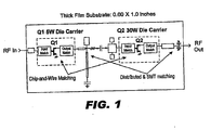
- Fig. 1 is a functional block diagram of a commercially available two stage thick film hybrid microelectronic amplifier (CREE PFM19030SM) which can advantageously be employed in a Doherty amplifier in accordance with an embodiment of the present invention.
- the first stage of the module includes a field effect transistor Q1 connected to a RF input through input matching circuitry and predistortion circuitry.
- the output of transistor Q1 is applied through an output matching network through distributed surface mount technology matching circuitry to the second stage including a second field effect transistor Q2.
- Transistor Q2 is connected to receive the output of Q1 through input matching circuitry and applies an amplified output through output matching circuitry to the RF output.
- the partitioning of this circuit places the devices with high power dissipation on metal interposers that constitute RF ground and also function as heat spreaders; while matching circuitry and bias injection and bypassing is realized using thick film microstrip circuits including SMT passive elements.
- the block diagram in Fig. 1 demonstrates the amplifier partitioning.
- Q1 and Q2 are LDMOS transistors, and each LDMOS transistor die exhibits input or output impedances on the order of 1-5 ohms (before adding chip and-wire matching).
- the combination of chip-and-wire matching and distributed circuit matching on the output of the 30W transistor (Q2) transforms the optimum powermatch impedance (for Class AB operation) to a nominal 20 Ohm level. This simplifies the off-module matching circuitry required for a Doherty amplifier subsystem.
- Each amplifier module assembly includes the two (5W and 30W) die carriers soldered to a bottom plate of copper (1.0 mm thick).
- the silicon LDMOS transistor die manufactured by Cree Microwave
- the bottom plate also supports a 0.5 mm thick single-layer alumina thick-film substrate which has cutouts where the die carriers are located.
- the alumina substrate is attached to the copper base with a conductive epoxy. The heat from the die is spread through the die carrier (interposer) and then through the thick copper base, before it encounters the external interface.
- the two-stage surface-mount module occupies only slightly more board space than would a single discrete-package 30W transistor (with conventional bolt-down metal flange).
- the first-stage drain and internal temperature compensation circuitry accessing the first-stage drain and internal temperature compensation circuitry.
- Bypass circuits are included internal to the module to support wide video bandwidths and thereby minimize memory effects.
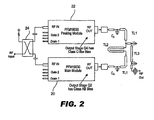
- Fig. 2 is a functional block diagram of a 2-way two stage Doherty amplifier in accordance with an embodiment of the present invention which employs two PFM19030SM modules of Fig. 1 .
- the amplifier includes a main module 20 and a peaking module 22 which receive an RF input signal through splitter 24.
- the main module 20 is biased for class AB operation, and the peak amplifier module is biased nominally for class C operation.
- Module inputs are connected directly to a 3 dB quadrature hybrid.
- the outputs are matched using short low impedance transmission line elements and shunt capacitors Cp and Cm. Because the output impedances of the modules are much higher than unmatched discrete LDMOS transistors, the additional matching circuitry is minimized.
- Cp and Cm are of different values (Cp ⁇ Cm) as is appropriate for the different operating modes (Class C vs. Class AB) of the 30W devices.
- transmission lines TL1 each side.
- the main module side TL2 section is nominally 90°, as is typical of classic 2-Way Doherty designs.
- the output section TL3 and associated capacitors constitute an impedance transformer. All element (transmission line and shunt capacitor) values are adjusted in the circuit analysis and optimization process. The validity and applications power of the CMC device models was confirmed by the experience that only capacitor values were adjusted in prototype circuitry to obtain reported results (transmission line lengths and widths were left at turn-on values).
- the capacitor values are adjusted primarily to achieve optimum peak power levels. Bias conditions are the most sensitive determinate of amplifier linearity and efficiency. By choosing Class AB & Class C, circuit linearity is optimized at some tradeoff in efficiency. Linearity is critical to the intended applications, in which further correction by pre-distortion can be anticipated. A major objective is to achieve system-level linearity standards with pre-distortion only (avoiding feed-forward losses). This strategy can potentially maximize system efficiency and reduce complexity.
- Gain and return loss for the two way, two stage amplifier of Fig. 2 are presented in Figure 3 .
- Gain is 26 ⁇ 0.2 dB over 1930-1960 MHz.
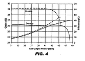
- Measured gain and efficiency versus CW output power are compared for the Doherty amplifier and an individual module operated with normal Class AB bias in Figure 4 .
- the Class AB module has a peak output capability on nominally 30 Watts (+44.8 dam), whereas the Doherty output is nominally 60 Watts (47.8 dam). Note that both circuits have device quiescent bias levels adjusted for optimum linearity, not for optimum peak power or for efficiency.
- the comparison of the shape of the efficiency versus output power characteristics is of particular interest. Even though the Doherty amplifier has twice the output power capability, its efficiency is similar to that of the individual module at low power levels.
- Figure 5 presents measured gain and relative phase versus output power (AM/PM) for the Doherty amplifier.
- AM/PM phase versus output power
- a characteristic of this 2-Way Doherty amplifier is the degradation of linearity as one deviates from the band center frequency. This is thought to be typical of 2-Way Doherty amplifiers in general. Center-band and band-edge measurements of CW 2-Tone 3rd order IMD products are included in Figure 7 . The 2-tone CW Imps show more dependence with frequency than do the 2-WCDMA signal tests.
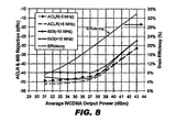
- Standard WCDMA testing involved two signals separated by 10 MHz (3GPP with 8.5 dB peak-to-average), centered at 1960 MHz. Measurements ( Fig 8 ) show that the IM3 products at 10 MHz offsets tend to be the dominant distortion, and a degree of IM3 asymmetry is evident at lower power levels (this also occurs for the individual modules operated in standard Class AB conditions). ACLR and IM3 rejection are plotted at three RF frequencies in Figure 9 . Measurement system dynamic range is limited to about -55 dab at low power( ⁇ -60 dab at higher power levels).
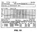
- Figure 10 shows 2-WCDMA signal data using a PMC-Sierra Paladin 15 digital pre-distortion to enhance the Doherty amplifier linearity.
- the signal in this case is two WCDMA signals with crestfactor reduction to 7.5 dB. Average output power is 12.5 Watts, and efficiency is 26.8%, with ACLR & IM3 at -51 & -54 dBc. Efficiency across the RF band varies from 28% to 26% (1930-1990), 1990), and ACLR is ⁇ 49 dBc and IM3 is ⁇ -50 dBc. IM3 asymmetry is very small after application of pre-D. This demonstrates excellent linearity and efficiency using this Doherty design in conjunction with pre-distortion.
- the two-way two stage Doherty amplifier in Fig.2 uses small surface-mount hybrid modules as the active elements in a 2-way 60W Doherty amplifier.
- the design demonstrates good efficiency (26%) for two 3GPP WCDMA signals at 10W average output, with ACLR of -40 dBc and IM3 of -38 dBc (uncorrected).
- 12.5W of WCDMA is produced at 26% efficiency & ACLR/IM3 rejections of -49 dBc/-50 dBc across the full 1930-1990 MHz band.
- the associated 26 dB gain and low input return loss simplifies system design.
- the transistors can be lateral DMOS silicon field effect transistors, MESFETs, HEMTs, HBTs, and bipolar transistors.
- the invention has been applicability to amplifiers having more than one peak amplifier and using modules with two or more stages. For example, a three way two stage amplifier using three CREE PFM19030 modules has been simulated for producing over 90 watts of single tone power with overall gain of 24 dB.
Landscapes
- Engineering & Computer Science (AREA)
- Power Engineering (AREA)
- Amplifiers (AREA)
- Transmitters (AREA)
Applications Claiming Priority (2)
| Application Number | Priority Date | Filing Date | Title |
|---|---|---|---|
| US11/090,577 US7193473B2 (en) | 2005-03-24 | 2005-03-24 | High power Doherty amplifier using multi-stage modules |
| EP06739337A EP1861920A4 (en) | 2005-03-24 | 2006-03-16 | DOHERTY HIGH-PERFORMANCE AMPLIFIERS WITH MULTI-STAGE MODULES |
Related Parent Applications (2)
| Application Number | Title | Priority Date | Filing Date |
|---|---|---|---|
| EP06739337.1 Division | 2006-03-16 | ||
| EP06739337A Division EP1861920A4 (en) | 2005-03-24 | 2006-03-16 | DOHERTY HIGH-PERFORMANCE AMPLIFIERS WITH MULTI-STAGE MODULES |
Publications (2)
| Publication Number | Publication Date |
|---|---|
| EP2442444A1 EP2442444A1 (en) | 2012-04-18 |
| EP2442444B1 true EP2442444B1 (en) | 2014-08-20 |
Family
ID=37024603
Family Applications (2)
| Application Number | Title | Priority Date | Filing Date |
|---|---|---|---|
| EP12150378.3A Active EP2442444B1 (en) | 2005-03-24 | 2006-03-16 | High power Doherty amplifier using multi-stage modules |
| EP06739337A Ceased EP1861920A4 (en) | 2005-03-24 | 2006-03-16 | DOHERTY HIGH-PERFORMANCE AMPLIFIERS WITH MULTI-STAGE MODULES |
Family Applications After (1)
| Application Number | Title | Priority Date | Filing Date |
|---|---|---|---|
| EP06739337A Ceased EP1861920A4 (en) | 2005-03-24 | 2006-03-16 | DOHERTY HIGH-PERFORMANCE AMPLIFIERS WITH MULTI-STAGE MODULES |
Country Status (5)
| Country | Link |
|---|---|
| US (1) | US7193473B2 (enExample) |
| EP (2) | EP2442444B1 (enExample) |
| JP (2) | JP2008535321A (enExample) |
| TW (1) | TWI377783B (enExample) |
| WO (1) | WO2006102466A2 (enExample) |
Cited By (2)
| Publication number | Priority date | Publication date | Assignee | Title |
|---|---|---|---|---|
| US11990871B2 (en) | 2017-04-24 | 2024-05-21 | Macom Technology Solutions Holdings, Inc. | Inverted Doherty power amplifier with large RF fractional and instantaneous bandwidths |
| US12028022B2 (en) | 2020-12-10 | 2024-07-02 | Macom Technology Solutions Holdings, Inc. | Hybrid power amplifier with GaN-on-Si and GaN-on-SiC circuits |
Families Citing this family (32)
| Publication number | Priority date | Publication date | Assignee | Title |
|---|---|---|---|---|
| JPWO2005093948A1 (ja) * | 2004-03-26 | 2008-02-14 | 株式会社日立国際電気 | 増幅器 |
| US7847630B2 (en) * | 2004-11-05 | 2010-12-07 | Hitachi Kokusai Electric Inc. | Amplifier |
| US7362170B2 (en) * | 2005-12-01 | 2008-04-22 | Andrew Corporation | High gain, high efficiency power amplifier |
| US7541866B2 (en) * | 2006-09-29 | 2009-06-02 | Nortel Networks Limited | Enhanced doherty amplifier with asymmetrical semiconductors |
| DE102006057324A1 (de) * | 2006-12-05 | 2008-06-19 | Rohde & Schwarz Gmbh & Co. Kg | Doherty-Verstärker-System |
| US9325280B2 (en) | 2007-09-03 | 2016-04-26 | Ampleon Netherlands B.V. | Multi-way doherty amplifier |
| US9479202B2 (en) * | 2008-02-19 | 2016-10-25 | Infineon Technologies Ag | System and method for burst mode amplifier |
| US7764120B2 (en) * | 2008-08-19 | 2010-07-27 | Cree, Inc. | Integrated circuit with parallel sets of transistor amplifiers having different turn on power levels |
| CN101582682B (zh) * | 2009-06-12 | 2011-12-28 | 华为技术有限公司 | 一种功率放大器和发射机 |
| WO2011046031A1 (ja) | 2009-10-13 | 2011-04-21 | 日本電気株式会社 | 電力増幅器およびその動作方法 |
| EP2393201A1 (en) | 2010-06-02 | 2011-12-07 | Nxp B.V. | Two stage doherty amplifier |
| DE102010034067A1 (de) * | 2010-08-12 | 2012-02-16 | Rohde & Schwarz Gmbh & Co. Kg | Hochfrequenzleistungsverstärker mit Doherty-Erweiterung |
| US8611834B2 (en) | 2010-11-01 | 2013-12-17 | Cree, Inc. | Matching network for transmission circuitry |
| US9071211B1 (en) * | 2011-12-15 | 2015-06-30 | Anadigics, Inc. | Compact doherty combiner |
| US8698560B2 (en) * | 2012-05-09 | 2014-04-15 | Mstar Semiconductor, Inc. | Variable-gain low noise amplifier |
| US8754710B2 (en) * | 2012-06-22 | 2014-06-17 | Mstar Semiconductor, Inc. | Low-noise amplifiers for RF receiver |
| CN202818232U (zh) * | 2012-09-18 | 2013-03-20 | 中兴通讯股份有限公司 | 一种Doherty功放电路 |
| US9007126B2 (en) | 2013-02-25 | 2015-04-14 | Intel Mobile Communications GmbH | Multi-mode amplifier system |
| US9407214B2 (en) | 2013-06-28 | 2016-08-02 | Cree, Inc. | MMIC power amplifier |
| US9030260B2 (en) * | 2013-07-19 | 2015-05-12 | Alcatel Lucent | Dual-band high efficiency Doherty amplifiers with hybrid packaged power devices |
| US11233483B2 (en) | 2017-02-02 | 2022-01-25 | Macom Technology Solutions Holdings, Inc. | 90-degree lumped and distributed Doherty impedance inverter |
| CN110785927B (zh) | 2017-04-24 | 2024-03-08 | 麦克姆技术解决方案控股有限公司 | 效率提高的对称多尔蒂功率放大器 |
| EP3616320B1 (en) * | 2017-04-24 | 2023-11-08 | MACOM Technology Solutions Holdings, Inc. | Inverted doherty power amplifier with large rf and instantaneous bandwidths |
| FR3070100A1 (fr) | 2017-08-14 | 2019-02-15 | Macom Technology Solutions Holdings, Inc. | Architecture d'amplificateur de puissance sans modulation, a large bande et a haut rendement |
| US11283410B2 (en) | 2017-10-02 | 2022-03-22 | Macom Technology Solutions Holdings, Inc. | No-load-modulation, high-efficiency power amplifier |
| US10250197B1 (en) | 2017-11-06 | 2019-04-02 | Nxp Usa, Inc. | Multiple-stage power amplifiers implemented with multiple semiconductor technologies |
| EP3480945A1 (en) | 2017-11-06 | 2019-05-08 | NXP USA, Inc. | Multiple-stage power amplifiers implemented with multiple semiconductor technologies |
| US10530306B2 (en) | 2018-04-13 | 2020-01-07 | Nxp Usa, Inc. | Hybrid power amplifier circuit or system with combination low-pass and high-pass interstage circuitry and method of operating same |
| EP3861633A1 (en) | 2018-10-05 | 2021-08-11 | MACOM Technology Solutions Holdings, Inc. | Low-load-modulation power amplifier |
| US12009788B2 (en) | 2019-03-28 | 2024-06-11 | Macom Technology Solutions Holdings, Inc. | In-transistor load modulation |
| US11888448B2 (en) | 2019-12-30 | 2024-01-30 | Macom Technology Solutions Holdings, Inc. | Low-load-modulation broadband amplifier |
| EP4297274A1 (en) | 2022-06-24 | 2023-12-27 | Wolfspeed, Inc. | Flip chip doherty amplifier devices |
Family Cites Families (17)
| Publication number | Priority date | Publication date | Assignee | Title |
|---|---|---|---|---|
| TW293899B (enExample) * | 1994-10-18 | 1996-12-21 | Seiko Epson Corp | |
| JP3135195B2 (ja) * | 1994-10-26 | 2001-02-13 | 三菱電機株式会社 | マイクロ波集積回路 |
| CA2204409A1 (en) * | 1995-11-30 | 1997-05-31 | James Frank Long | Amplifier circuit and method of tuning the amplifier circuit |
| US5786727A (en) * | 1996-10-15 | 1998-07-28 | Motorola, Inc. | Multi-stage high efficiency linear power amplifier and method therefor |
| US6262629B1 (en) * | 1999-07-06 | 2001-07-17 | Motorola, Inc. | High efficiency power amplifier having reduced output matching networks for use in portable devices |
| EP1104093A1 (en) * | 1999-11-24 | 2001-05-30 | Telefonaktiebolaget Lm Ericsson | Method and apparatus for generation of a RF signal |
| US6320462B1 (en) * | 2000-04-12 | 2001-11-20 | Raytheon Company | Amplifier circuit |
| US6864742B2 (en) * | 2001-06-08 | 2005-03-08 | Northrop Grumman Corporation | Application of the doherty amplifier as a predistortion circuit for linearizing microwave amplifiers |
| US6737922B2 (en) * | 2002-01-28 | 2004-05-18 | Cree Microwave, Inc. | N-way RF power amplifier circuit with increased back-off capability and power added efficiency using unequal input power division |
| US6791417B2 (en) * | 2002-01-28 | 2004-09-14 | Cree Microwave, Inc. | N-way RF power amplifier circuit with increased back-off capability and power added efficiency using selected phase lengths and output impedances |
| US6700444B2 (en) * | 2002-01-28 | 2004-03-02 | Cree Microwave, Inc. | N-way RF power amplifier with increased backoff power and power added efficiency |
| KR100553252B1 (ko) * | 2002-02-01 | 2006-02-20 | 아바고테크놀로지스코리아 주식회사 | 휴대용 단말기의 전력 증폭 장치 |
| GB2393866A (en) * | 2002-09-06 | 2004-04-07 | Filtronic Plc | A class F Doherty amplifier using PHEMTs |
| US6822321B2 (en) * | 2002-09-30 | 2004-11-23 | Cree Microwave, Inc. | Packaged RF power transistor having RF bypassing/output matching network |
| KR100480496B1 (ko) * | 2002-11-18 | 2005-04-07 | 학교법인 포항공과대학교 | 도허티 증폭기를 이용한 신호 증폭 장치 |
| US6798295B2 (en) * | 2002-12-13 | 2004-09-28 | Cree Microwave, Inc. | Single package multi-chip RF power amplifier |
| JP2004222151A (ja) * | 2003-01-17 | 2004-08-05 | Nec Corp | ドハーティ増幅器 |
-
2005
- 2005-03-24 US US11/090,577 patent/US7193473B2/en not_active Expired - Lifetime
-
2006
- 2006-03-16 JP JP2008503161A patent/JP2008535321A/ja active Pending
- 2006-03-16 EP EP12150378.3A patent/EP2442444B1/en active Active
- 2006-03-16 WO PCT/US2006/010498 patent/WO2006102466A2/en not_active Ceased
- 2006-03-16 EP EP06739337A patent/EP1861920A4/en not_active Ceased
- 2006-03-21 TW TW095109664A patent/TWI377783B/zh active
-
2009
- 2009-06-29 JP JP2009153975A patent/JP2009219161A/ja active Pending
Cited By (2)
| Publication number | Priority date | Publication date | Assignee | Title |
|---|---|---|---|---|
| US11990871B2 (en) | 2017-04-24 | 2024-05-21 | Macom Technology Solutions Holdings, Inc. | Inverted Doherty power amplifier with large RF fractional and instantaneous bandwidths |
| US12028022B2 (en) | 2020-12-10 | 2024-07-02 | Macom Technology Solutions Holdings, Inc. | Hybrid power amplifier with GaN-on-Si and GaN-on-SiC circuits |
Also Published As
| Publication number | Publication date |
|---|---|
| US7193473B2 (en) | 2007-03-20 |
| EP1861920A4 (en) | 2009-12-02 |
| EP1861920A2 (en) | 2007-12-05 |
| EP2442444A1 (en) | 2012-04-18 |
| US20060214732A1 (en) | 2006-09-28 |
| WO2006102466A3 (en) | 2007-04-05 |
| JP2009219161A (ja) | 2009-09-24 |
| TW200703886A (en) | 2007-01-16 |
| JP2008535321A (ja) | 2008-08-28 |
| TWI377783B (en) | 2012-11-21 |
| WO2006102466A2 (en) | 2006-09-28 |
Similar Documents
| Publication | Publication Date | Title |
|---|---|---|
| EP2442444B1 (en) | High power Doherty amplifier using multi-stage modules | |
| JP2945833B2 (ja) | マイクロ波ドハティ型増幅器 | |
| Rostomyan et al. | 28 GHz Doherty power amplifier in CMOS SOI with 28% back-off PAE | |
| CN108512514B (zh) | 多级rf放大器装置 | |
| Kang et al. | Design of bandwidth-enhanced Doherty power amplifiers for handset applications | |
| US11716058B2 (en) | No-load-modulation, high-efficiency power amplifier | |
| Van Der Heijden et al. | A 19W high-efficiency wide-band CMOS-GaN class-E Chireix RF outphasing power amplifier | |
| US20220123693A1 (en) | Doherty power amplifiers and devices with low voltage driver stage in carrier-path and high voltage driver stage in peaking-path | |
| EP3014766A1 (en) | Mmic power amplifier | |
| Yamaguchi et al. | A wideband and high efficiency Ka-band GaN Doherty power amplifier for 5G communications | |
| Wohlert et al. | 8-Watt linear three-stage GaN Doherty power amplifier for 28 GHz 5G applications | |
| CN110785926A (zh) | 具有大rf分数和瞬时带宽的反向多尔蒂功率放大器 | |
| CN110785928A (zh) | 具有大rf分数和瞬时带宽的反向多尔蒂功率放大器 | |
| CN101836357A (zh) | 功率放大器 | |
| Nakatani et al. | A Ka-band CW 15.5 W 15.6% fractional bandwidth GaN power amplifier MMIC using wideband BPF inter-stage matching network | |
| Wei et al. | High efficiency linear GaAs MMIC amplifier for wireless base station and Femto cell applications | |
| Jeong et al. | AlGaN/GaN based ultra‐wideband 15‐W high‐power amplifier with improved return loss | |
| Kimball et al. | High efficiency WCDMA envelope tracking base-station amplifier implemented with GaAs HVHBTs | |
| Darraji et al. | Generic load-pull-based design methodology for performance optimisation of Doherty amplifiers | |
| Crescenzi et al. | 60 Watt Doherty amplifiers using high gain 2-stage hybrid amplifier modules | |
| Katz et al. | GaN SSPA for UHF space applications | |
| Courty et al. | A 3.7-4.2 GHz MMIC Doherty Power Amplifier Linearized over 500MHz Instantaneous Bandwidth | |
| CN223514868U (zh) | 功率放大器和射频前端模组 | |
| US12155356B2 (en) | Monolithic microwave integrated circuit device with internal decoupling capacitor | |
| Samanta | High Power Wide-Band GaN Amplifiers: Industrial Design and Challenges |
Legal Events
| Date | Code | Title | Description |
|---|---|---|---|
| PUAI | Public reference made under article 153(3) epc to a published international application that has entered the european phase |
Free format text: ORIGINAL CODE: 0009012 |
|
| AC | Divisional application: reference to earlier application |
Ref document number: 1861920 Country of ref document: EP Kind code of ref document: P |
|
| AK | Designated contracting states |
Kind code of ref document: A1 Designated state(s): AT BE BG CH CY CZ DE DK EE ES FI FR GB GR HU IE IS IT LI LT LU LV MC NL PL PT RO SE SI SK TR |
|
| 17P | Request for examination filed |
Effective date: 20121005 |
|
| 17Q | First examination report despatched |
Effective date: 20121023 |
|
| GRAP | Despatch of communication of intention to grant a patent |
Free format text: ORIGINAL CODE: EPIDOSNIGR1 |
|
| INTG | Intention to grant announced |
Effective date: 20140303 |
|
| GRAS | Grant fee paid |
Free format text: ORIGINAL CODE: EPIDOSNIGR3 |
|
| GRAA | (expected) grant |
Free format text: ORIGINAL CODE: 0009210 |
|
| AC | Divisional application: reference to earlier application |
Ref document number: 1861920 Country of ref document: EP Kind code of ref document: P |
|
| AK | Designated contracting states |
Kind code of ref document: B1 Designated state(s): AT BE BG CH CY CZ DE DK EE ES FI FR GB GR HU IE IS IT LI LT LU LV MC NL PL PT RO SE SI SK TR |
|
| REG | Reference to a national code |
Ref country code: GB Ref legal event code: FG4D |
|
| REG | Reference to a national code |
Ref country code: CH Ref legal event code: EP |
|
| REG | Reference to a national code |
Ref country code: AT Ref legal event code: REF Ref document number: 683920 Country of ref document: AT Kind code of ref document: T Effective date: 20140915 |
|
| REG | Reference to a national code |
Ref country code: IE Ref legal event code: FG4D |
|
| REG | Reference to a national code |
Ref country code: DE Ref legal event code: R096 Ref document number: 602006042814 Country of ref document: DE Effective date: 20141002 |
|
| REG | Reference to a national code |
Ref country code: SE Ref legal event code: TRGR |
|
| REG | Reference to a national code |
Ref country code: NL Ref legal event code: T3 |
|
| REG | Reference to a national code |
Ref country code: AT Ref legal event code: MK05 Ref document number: 683920 Country of ref document: AT Kind code of ref document: T Effective date: 20140820 |
|
| REG | Reference to a national code |
Ref country code: LT Ref legal event code: MG4D |
|
| PG25 | Lapsed in a contracting state [announced via postgrant information from national office to epo] |
Ref country code: ES Free format text: LAPSE BECAUSE OF FAILURE TO SUBMIT A TRANSLATION OF THE DESCRIPTION OR TO PAY THE FEE WITHIN THE PRESCRIBED TIME-LIMIT Effective date: 20140820 Ref country code: PT Free format text: LAPSE BECAUSE OF FAILURE TO SUBMIT A TRANSLATION OF THE DESCRIPTION OR TO PAY THE FEE WITHIN THE PRESCRIBED TIME-LIMIT Effective date: 20141222 Ref country code: GR Free format text: LAPSE BECAUSE OF FAILURE TO SUBMIT A TRANSLATION OF THE DESCRIPTION OR TO PAY THE FEE WITHIN THE PRESCRIBED TIME-LIMIT Effective date: 20141121 Ref country code: LT Free format text: LAPSE BECAUSE OF FAILURE TO SUBMIT A TRANSLATION OF THE DESCRIPTION OR TO PAY THE FEE WITHIN THE PRESCRIBED TIME-LIMIT Effective date: 20140820 Ref country code: BG Free format text: LAPSE BECAUSE OF FAILURE TO SUBMIT A TRANSLATION OF THE DESCRIPTION OR TO PAY THE FEE WITHIN THE PRESCRIBED TIME-LIMIT Effective date: 20141120 |
|
| PG25 | Lapsed in a contracting state [announced via postgrant information from national office to epo] |
Ref country code: IS Free format text: LAPSE BECAUSE OF FAILURE TO SUBMIT A TRANSLATION OF THE DESCRIPTION OR TO PAY THE FEE WITHIN THE PRESCRIBED TIME-LIMIT Effective date: 20141220 Ref country code: LV Free format text: LAPSE BECAUSE OF FAILURE TO SUBMIT A TRANSLATION OF THE DESCRIPTION OR TO PAY THE FEE WITHIN THE PRESCRIBED TIME-LIMIT Effective date: 20140820 Ref country code: AT Free format text: LAPSE BECAUSE OF FAILURE TO SUBMIT A TRANSLATION OF THE DESCRIPTION OR TO PAY THE FEE WITHIN THE PRESCRIBED TIME-LIMIT Effective date: 20140820 |
|
| PG25 | Lapsed in a contracting state [announced via postgrant information from national office to epo] |
Ref country code: RO Free format text: LAPSE BECAUSE OF FAILURE TO SUBMIT A TRANSLATION OF THE DESCRIPTION OR TO PAY THE FEE WITHIN THE PRESCRIBED TIME-LIMIT Effective date: 20140820 Ref country code: IT Free format text: LAPSE BECAUSE OF FAILURE TO SUBMIT A TRANSLATION OF THE DESCRIPTION OR TO PAY THE FEE WITHIN THE PRESCRIBED TIME-LIMIT Effective date: 20140820 Ref country code: EE Free format text: LAPSE BECAUSE OF FAILURE TO SUBMIT A TRANSLATION OF THE DESCRIPTION OR TO PAY THE FEE WITHIN THE PRESCRIBED TIME-LIMIT Effective date: 20140820 Ref country code: DK Free format text: LAPSE BECAUSE OF FAILURE TO SUBMIT A TRANSLATION OF THE DESCRIPTION OR TO PAY THE FEE WITHIN THE PRESCRIBED TIME-LIMIT Effective date: 20140820 Ref country code: SK Free format text: LAPSE BECAUSE OF FAILURE TO SUBMIT A TRANSLATION OF THE DESCRIPTION OR TO PAY THE FEE WITHIN THE PRESCRIBED TIME-LIMIT Effective date: 20140820 Ref country code: CZ Free format text: LAPSE BECAUSE OF FAILURE TO SUBMIT A TRANSLATION OF THE DESCRIPTION OR TO PAY THE FEE WITHIN THE PRESCRIBED TIME-LIMIT Effective date: 20140820 |
|
| REG | Reference to a national code |
Ref country code: DE Ref legal event code: R097 Ref document number: 602006042814 Country of ref document: DE |
|
| PG25 | Lapsed in a contracting state [announced via postgrant information from national office to epo] |
Ref country code: PL Free format text: LAPSE BECAUSE OF FAILURE TO SUBMIT A TRANSLATION OF THE DESCRIPTION OR TO PAY THE FEE WITHIN THE PRESCRIBED TIME-LIMIT Effective date: 20140820 |
|
| PLBE | No opposition filed within time limit |
Free format text: ORIGINAL CODE: 0009261 |
|
| STAA | Information on the status of an ep patent application or granted ep patent |
Free format text: STATUS: NO OPPOSITION FILED WITHIN TIME LIMIT |
|
| 26N | No opposition filed |
Effective date: 20150521 |
|
| PG25 | Lapsed in a contracting state [announced via postgrant information from national office to epo] |
Ref country code: MC Free format text: LAPSE BECAUSE OF FAILURE TO SUBMIT A TRANSLATION OF THE DESCRIPTION OR TO PAY THE FEE WITHIN THE PRESCRIBED TIME-LIMIT Effective date: 20140820 Ref country code: LU Free format text: LAPSE BECAUSE OF FAILURE TO SUBMIT A TRANSLATION OF THE DESCRIPTION OR TO PAY THE FEE WITHIN THE PRESCRIBED TIME-LIMIT Effective date: 20150316 |
|
| REG | Reference to a national code |
Ref country code: CH Ref legal event code: PL |
|
| GBPC | Gb: european patent ceased through non-payment of renewal fee |
Effective date: 20150316 |
|
| PG25 | Lapsed in a contracting state [announced via postgrant information from national office to epo] |
Ref country code: SI Free format text: LAPSE BECAUSE OF FAILURE TO SUBMIT A TRANSLATION OF THE DESCRIPTION OR TO PAY THE FEE WITHIN THE PRESCRIBED TIME-LIMIT Effective date: 20140820 |
|
| REG | Reference to a national code |
Ref country code: IE Ref legal event code: MM4A |
|
| PG25 | Lapsed in a contracting state [announced via postgrant information from national office to epo] |
Ref country code: LI Free format text: LAPSE BECAUSE OF NON-PAYMENT OF DUE FEES Effective date: 20150331 Ref country code: CH Free format text: LAPSE BECAUSE OF NON-PAYMENT OF DUE FEES Effective date: 20150331 Ref country code: IE Free format text: LAPSE BECAUSE OF NON-PAYMENT OF DUE FEES Effective date: 20150316 Ref country code: GB Free format text: LAPSE BECAUSE OF NON-PAYMENT OF DUE FEES Effective date: 20150316 |
|
| REG | Reference to a national code |
Ref country code: FR Ref legal event code: PLFP Year of fee payment: 11 |
|
| PG25 | Lapsed in a contracting state [announced via postgrant information from national office to epo] |
Ref country code: BE Free format text: LAPSE BECAUSE OF FAILURE TO SUBMIT A TRANSLATION OF THE DESCRIPTION OR TO PAY THE FEE WITHIN THE PRESCRIBED TIME-LIMIT Effective date: 20140820 |
|
| REG | Reference to a national code |
Ref country code: FR Ref legal event code: PLFP Year of fee payment: 12 |
|
| PG25 | Lapsed in a contracting state [announced via postgrant information from national office to epo] |
Ref country code: HU Free format text: LAPSE BECAUSE OF FAILURE TO SUBMIT A TRANSLATION OF THE DESCRIPTION OR TO PAY THE FEE WITHIN THE PRESCRIBED TIME-LIMIT; INVALID AB INITIO Effective date: 20060316 |
|
| PG25 | Lapsed in a contracting state [announced via postgrant information from national office to epo] |
Ref country code: CY Free format text: LAPSE BECAUSE OF FAILURE TO SUBMIT A TRANSLATION OF THE DESCRIPTION OR TO PAY THE FEE WITHIN THE PRESCRIBED TIME-LIMIT Effective date: 20140820 |
|
| PG25 | Lapsed in a contracting state [announced via postgrant information from national office to epo] |
Ref country code: TR Free format text: LAPSE BECAUSE OF FAILURE TO SUBMIT A TRANSLATION OF THE DESCRIPTION OR TO PAY THE FEE WITHIN THE PRESCRIBED TIME-LIMIT Effective date: 20140820 |
|
| REG | Reference to a national code |
Ref country code: FR Ref legal event code: PLFP Year of fee payment: 13 |
|
| REG | Reference to a national code |
Ref country code: NL Ref legal event code: HC Owner name: WOLFSPEED, INC.; US Free format text: DETAILS ASSIGNMENT: CHANGE OF OWNER(S), CHANGE OF OWNER(S) NAME; FORMER OWNER NAME: CREE MICROWAVE, INC. Effective date: 20240529 |
|
| REG | Reference to a national code |
Ref country code: DE Ref legal event code: R081 Ref document number: 602006042814 Country of ref document: DE Owner name: WOLFSPEED, INC., DURHAM, US Free format text: FORMER OWNER: CREE, INC., DURHAM, NC, US Ref country code: DE Ref legal event code: R081 Ref document number: 602006042814 Country of ref document: DE Owner name: WOLFSPEED, INC., DURHAM, US Free format text: FORMER OWNERS: CREE, INC., DURHAM, NC, US; CREE MICROWAVE, LLC, DURHAM, NC, US Ref country code: DE Ref legal event code: R081 Ref document number: 602006042814 Country of ref document: DE Owner name: WOLFSPEED, INC., DURHAM, US Free format text: FORMER OWNERS: CREE, INC., DURHAM, NC, US; CREE MICROWAVE, INC., DURHAM, NC, US Ref country code: DE Ref legal event code: R081 Ref document number: 602006042814 Country of ref document: DE Owner name: WOLFSPEED, INC., DURHAM, US Free format text: FORMER OWNERS: CREE, INC., DURHAM, N.C., US; CREE MICROWAVE, INC., SUNNYVALE, CALIF., US |
|
| REG | Reference to a national code |
Ref country code: NL Ref legal event code: PD Owner name: MACOM TECHNOLOGY SOLUTIONS HOLDINGS, INC.; US Free format text: DETAILS ASSIGNMENT: CHANGE OF OWNER(S), ASSIGNMENT; FORMER OWNER NAME: WOLFSPEED, INC. Effective date: 20250326 |
|
| PGFP | Annual fee paid to national office [announced via postgrant information from national office to epo] |
Ref country code: SE Payment date: 20250321 Year of fee payment: 20 |
|
| PGFP | Annual fee paid to national office [announced via postgrant information from national office to epo] |
Ref country code: DE Payment date: 20250319 Year of fee payment: 20 |
|
| PGFP | Annual fee paid to national office [announced via postgrant information from national office to epo] |
Ref country code: FI Payment date: 20250324 Year of fee payment: 20 Ref country code: NL Payment date: 20250319 Year of fee payment: 20 |
|
| PGFP | Annual fee paid to national office [announced via postgrant information from national office to epo] |
Ref country code: FR Payment date: 20250325 Year of fee payment: 20 |
|
| REG | Reference to a national code |
Ref country code: FI Ref legal event code: PCE Owner name: MACOM TECHNOLOGY SOLUTIONS HOLDINGS, INC.; CREE MICROWAVE, INC. |