EP2437485A2 - Strahlenabbildungsvorrichtung und Steuerungsverfahren für die Strahlenabbildungsvorrichtung - Google Patents
Strahlenabbildungsvorrichtung und Steuerungsverfahren für die Strahlenabbildungsvorrichtung Download PDFInfo
- Publication number
- EP2437485A2 EP2437485A2 EP11182110A EP11182110A EP2437485A2 EP 2437485 A2 EP2437485 A2 EP 2437485A2 EP 11182110 A EP11182110 A EP 11182110A EP 11182110 A EP11182110 A EP 11182110A EP 2437485 A2 EP2437485 A2 EP 2437485A2
- Authority
- EP
- European Patent Office
- Prior art keywords
- imaging
- signal
- pixel
- time
- voltage
- Prior art date
- Legal status (The legal status is an assumption and is not a legal conclusion. Google has not performed a legal analysis and makes no representation as to the accuracy of the status listed.)
- Withdrawn
Links
Images


Classifications
-
- H—ELECTRICITY
- H04—ELECTRIC COMMUNICATION TECHNIQUE
- H04N—PICTORIAL COMMUNICATION, e.g. TELEVISION
- H04N25/00—Circuitry of solid-state image sensors [SSIS]; Control thereof
- H04N25/30—Circuitry of solid-state image sensors [SSIS]; Control thereof for transforming X-rays into image signals
-
- H—ELECTRICITY
- H04—ELECTRIC COMMUNICATION TECHNIQUE
- H04N—PICTORIAL COMMUNICATION, e.g. TELEVISION
- H04N25/00—Circuitry of solid-state image sensors [SSIS]; Control thereof
- H04N25/70—SSIS architectures; Circuits associated therewith
- H04N25/76—Addressed sensors, e.g. MOS or CMOS sensors
- H04N25/77—Pixel circuitry, e.g. memories, A/D converters, pixel amplifiers, shared circuits or shared components
- H04N25/778—Pixel circuitry, e.g. memories, A/D converters, pixel amplifiers, shared circuits or shared components comprising amplifiers shared between a plurality of pixels, i.e. at least one part of the amplifier must be on the sensor array itself
-
- H—ELECTRICITY
- H04—ELECTRIC COMMUNICATION TECHNIQUE
- H04N—PICTORIAL COMMUNICATION, e.g. TELEVISION
- H04N23/00—Cameras or camera modules comprising electronic image sensors; Control thereof
- H04N23/30—Cameras or camera modules comprising electronic image sensors; Control thereof for generating image signals from X-rays
-
- H—ELECTRICITY
- H04—ELECTRIC COMMUNICATION TECHNIQUE
- H04N—PICTORIAL COMMUNICATION, e.g. TELEVISION
- H04N25/00—Circuitry of solid-state image sensors [SSIS]; Control thereof
- H04N25/60—Noise processing, e.g. detecting, correcting, reducing or removing noise
- H04N25/616—Noise processing, e.g. detecting, correcting, reducing or removing noise involving a correlated sampling function, e.g. correlated double sampling [CDS] or triple sampling
-
- H—ELECTRICITY
- H04—ELECTRIC COMMUNICATION TECHNIQUE
- H04N—PICTORIAL COMMUNICATION, e.g. TELEVISION
- H04N25/00—Circuitry of solid-state image sensors [SSIS]; Control thereof
- H04N25/60—Noise processing, e.g. detecting, correcting, reducing or removing noise
- H04N25/618—Noise processing, e.g. detecting, correcting, reducing or removing noise for random or high-frequency noise
-
- H—ELECTRICITY
- H04—ELECTRIC COMMUNICATION TECHNIQUE
- H04N—PICTORIAL COMMUNICATION, e.g. TELEVISION
- H04N25/00—Circuitry of solid-state image sensors [SSIS]; Control thereof
- H04N25/60—Noise processing, e.g. detecting, correcting, reducing or removing noise
- H04N25/62—Detection or reduction of noise due to excess charges produced by the exposure, e.g. smear, blooming, ghost image, crosstalk or leakage between pixels
-
- H—ELECTRICITY
- H04—ELECTRIC COMMUNICATION TECHNIQUE
- H04N—PICTORIAL COMMUNICATION, e.g. TELEVISION
- H04N25/00—Circuitry of solid-state image sensors [SSIS]; Control thereof
- H04N25/60—Noise processing, e.g. detecting, correcting, reducing or removing noise
- H04N25/67—Noise processing, e.g. detecting, correcting, reducing or removing noise applied to fixed-pattern noise, e.g. non-uniformity of response
- H04N25/671—Noise processing, e.g. detecting, correcting, reducing or removing noise applied to fixed-pattern noise, e.g. non-uniformity of response for non-uniformity detection or correction
- H04N25/677—Noise processing, e.g. detecting, correcting, reducing or removing noise applied to fixed-pattern noise, e.g. non-uniformity of response for non-uniformity detection or correction for reducing the column or line fixed pattern noise
Definitions
- the present invention relates to a radiation imaging apparatus and a control method for the radiation imaging apparatus.
- Imaging apparatuses using photoelectric conversion elements include amorphous silicon type apparatuses, CCD type apparatuses, and CMOS type apparatuses. Imaging elements using amorphous silicon semiconductors on a glass substrate allow to easily form a large-area imaging apparatus. On the other hand, as compared with a single-crystal silicon semiconductor substrate, amorphous silicon makes it difficult to microfabricate a semiconductor substrate on a glass substrate.
- Japanese Patent Laid-Open No. 2002-344809 discloses a large-area flat panel type sensor, which implements large-area imaging by using CMOS type imaging elements as photoelectric conversion elements, more specifically by tiling rectangular imaging elements which are rectangular CMOS type photoelectric conversion elements cut out from a silicon semiconductor wafer.
- a CMOS type imaging element is capable of fast readout owing to microfabrication as compared with amorphous silicon, and hence allows to obtain higher sensitivity.
- a CMOS type imaging element is known as being highly advantageous when implementing a large-area flat panel type sensor. This is because this element is free from the problems of the number of transfer stages for electric charge transfer and power consumption unlike a CCD imaging element, and hence facilitates the implementation of large-area imaging.
- Japanese Patent Laid-Open No. 2006-319529 discloses an arrangement using a pixel addition circuit in a CMOS type imaging element and a sensitivity switch.
- CMOS type imaging element which implements both pixel addition and sensitivity switching.
- this element when, for example, this element is driven in a high sensitivity mode, the sensitivity switch is turned off, and one end of a dynamic range expansion capacitor is opened to become floating.
- the electric charge accumulated in this floating capacitor is unstable, and hence unstable voltages are generated in the circuit of the CMOS type imaging element.
- unstable voltages are generated in the circuit of a CMOS type imaging element in moving image capturing operation, a small amount of leakage between the gate and source of each MOS transistor in the circuit of the CMOS type imaging element becomes unstable, resulting in random noise affecting each frame.
- a CMOS type imaging element has an offset value, and each pixel outputs a non-zero value as an optical signal even without application of light.
- a method of defining optical signal data acquired without application of light as a fixed pattern noise (FPN) pattern of a CMOS type imaging element and subtracting the FPN pattern from optical signal data obtained when acquiring a moving image.
- FPN fixed pattern noise
- the electric potential of each floating portion for each moving image capturing operation changes with time, the electric potential of the floating portion in the CMOS type imaging element which has acquired an FPN pattern before imaging operation differs from the electric potential of the floating portion which is set when a moving image is actually acquired. This causes a difference between the FPN pattern and a noise component derived from the unstable voltage of the floating portion in moving image data subjected to FPN correction, resulting in a failure to perform proper FPN correction.
- the present invention provides a radiation imaging apparatus which can reduce noise components by fixing the unstable voltage of each floating portion in a pixel circuit of a CMOS type imaging element by electric potential fixing driving (electric potential fixing driving operation) of performing driving operation of fixing the unstable voltage of each floating portion in the pixel circuit to a predetermined voltage of a power supply at a timing before the imaging operation by an imaging unit.
- electric potential fixing driving electric potential fixing driving operation
- the present invention in its first aspect provides a radiation imaging apparatus as specified in claims 1 to 7.
- the present invention in its second aspect provides a control method for a radiation imaging apparatus as specified in claim 8.
- the present invention it is possible to reduce noise components by fixing the unstable voltage of each floating portion in a pixel circuit at a predetermined voltage of a power supply at a timing before imaging operation by an imaging unit.
- Fig. 1 is a timing chart showing the driving timing of a pixel circuit in the first embodiment
- Fig. 2 is a timing chart showing the driving timing of a pixel circuit in the second embodiment
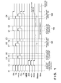
- Fig. 3 is a block diagram showing the schematic arrangement of a radiation imaging apparatus according to the third embodiment
- Fig. 4 is a block diagram showing the schematic arrangement of a radiation imaging apparatus according to the fourth embodiment.
- Fig. 5 is a view showing a driving procedure in an imaging control unit in a radiation imaging apparatus according to the fourth embodiment
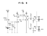
- Fig. 6 is a circuit diagram showing an example of the arrangement of a pixel circuit of a CMOS imaging element
- Fig. 7 is a timing chart of the driving timing of a pixel circuit of the CMOS imaging element
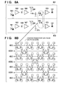
- Fig. 8A is a circuit diagram showing an example of the arrangement of addition circuits in pixel circuits of the CMOS type imaging element
- Fig. 8B is a view showing the schematic arrangement of CMOS type imaging elements connected via addition circuits;
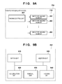
- Fig. 9A is a block diagram showing an example of the arrangement of the radiation imaging apparatus according to the first embodiment.
- Fig. 9B is a block diagram showing the functional arrangement of a pixel circuit corresponding to one pixel of the CMOS type imaging element.
- Figs. 9A and 9B show the arrangement of a radiation imaging apparatus 204 according to an embodiment of the present invention.
- the radiation imaging apparatus 204 shown in Fig. 9A includes an imaging unit 210 constituted by a plurality of CMOS type imaging elements 202, and an imaging control unit 201 which controls the operation of each of the plurality of CMOS type imaging elements 202.
- Fig. 9B shows the functional arrangement of a pixel circuit corresponding to one pixel of a CMOS type imaging element used for tiling of rectangular imaging elements obtained by cutting out CMOS type imaging elements in a rectangular shape from a wafer.
- the imaging unit 210 is constituted by pixel circuits arranged in m rows x n columns (where m and n are natural numbers equal to or more than two).
- a switch unit 910 of each pixel circuit is connected to a power supply for applying a predetermined voltage at the time of operation, and disconnected from the power supply at the time of non-operation.
- An accumulation unit 920 accumulates a signal corresponding to one pixel corresponding to an input radiation signal.
- a removal unit 930 removes noise from the signal accumulated in the accumulation unit 920.
- a holding unit 940 can hold the signal from which the noise is removed by the removal unit 930, and output the signal.
- An addition unit 950 performs addition processing for the signal held by the holding unit 940 and the signals held by the holding units of a ( a is a natural number equal to or more than two) adjacent other pixel circuits.
- the imaging control unit 201 can control the operation of each of the pixel circuits constituting the imaging unit 210. At a timing before imaging operation by the imaging unit 210, the imaging control unit 201 causes the switch unit 910, accumulation unit 920, removal unit 930, holding unit 940, and addition unit 950, which constitute each pixel circuit, to operate.
- the imaging control unit 201 sets a predetermined voltage of a power supply connected via the switch unit 910 in the accumulation unit 920, removal unit 930, holding unit 940, and addition unit 950 (electric potential fixing driving operation).
- Performing electric potential fixing driving operation at a timing before imaging by the imaging unit 210 can reduce noise components and accurately correct fixed pattern noise by fixing the unstable voltages of the accumulation unit 920, removal unit 930, holding unit 940, and addition unit 950 in the pixel circuit to a predetermined voltage of the power supply.
- Electric potential fixing driving operation will be described below with reference to a specific circuit arrangement of a CMOS imaging element.
- Fig. 6 is a circuit diagram showing an example of a pixel circuit corresponding to one pixel of a CMOS type imaging element used for tiling of rectangular imaging elements obtained by cutting out CMOS type imaging elements in a rectangular shape from a wafer.
- reference symbol PD denotes a photodiode which performs photoelectric conversion
- Cfd the capacitance of a floating diffusion region which accumulates electric charge in accordance with an optical signal converted from a radiation signal by the photodiode PD
- M2 a reset MOS transistor (reset switch) for removing the electric charge accumulated in the floating diffusion region.
- the reset switch M2 is connected to the first power supply for applying a reset voltage VRES as a predetermined voltage at the time of operation, and is disconnected from the first power supply at the time of non-operation.
- Reference symbol M1 denotes a sensitivity switching MOS transistor (sensitivity switch) for switching and setting a high dynamic range mode and a high sensitivity mode; and C1, a dynamic range expansion capacitor which can accumulate electric charge when the sensitivity switch M1 is turned on.
- the capacitance Cfd of the electric charge accumulation unit floating diffusion region
- the sensitivity switch M1 is turned off.
- the sensitivity switch M1 is turned on.
- Reference symbol M4 denotes an amplifying MOS transistor (first pixel amplifier) which operates as a source follower; and M3, a selection MOS transistor (selection switch) for activating the first pixel amplifier M4.
- the subsequent stage of the first pixel amplifier M4 is provided with a clamp circuit (noise removal circuit) which removes reset noise (kTC noise) generated upon connection to the reset voltage VRES by ON operation of the reset switch M2.
- Reference symbol Ccl denotes a clamp capacitor; and M5, a clamp MOS transistor (clamp switch).
- the clamp switch M5 is connected to the second power supply for applying a clamp voltage VCL as a predetermined voltage at the time of operation, and disconnected from the second power supply at the time of non-operation.
- Reference symbol M7 denotes an amplifying MOS transistor (second pixel amplifier) which operates as a source follower; and M6, a selection MOS transistor (selection switch) for activating the second pixel amplifier M7.
- the subsequent stage of the second pixel amplifier M7 is provided with two sample and hold circuits.
- Reference symbol M8 denotes a sample and hold MOS transistor (sample and hold switch) which forms a sample and hold circuit (first sample and hold circuit) for optical signal accumulation;
- CS an optical signal hold capacitor;
- M11 a sample and hold MOS transistor (sample and hold switch) which forms a noise signal accumulation sample and hold circuit (second sample and hold circuit);
- CN a noise signal hold capacitor;
- M10 an optical signal amplifying MOS transistor (pixel amplifier) which operates as a source follower.
- the pixel amplifier M10 (third pixel amplifier) outputs the optical signal voltage held by the optical signal accumulation sample and hold circuit (first sample and hold circuit).
- Reference symbol M9 denotes an analog switch (transfer switch) for outputting the optical signal amplified by the pixel amplifier M10 to the S signal output line; and M13, a noise signal amplifying MOS transistor (pixel amplifier) which operates as a source follower.
- the pixel amplifier M13 (fourth pixel amplifier) outputs the noise signal voltage held by the noise signal accumulation sample and hold circuit (second sample and hold circuit).
- Reference symbol M12 denotes an analog switch (transfer switch) for outputting the noise signal amplified by the pixel amplifier M13 to the N signal output line.
- An EN signal input unit is connected to the gates of the selection switch M3 and selection switch M6.
- the EN signal input from the EN signal input unit controls the operation states of the first pixel amplifier M4 and second pixel amplifier M7.
- the EN signal is set at high level, the first pixel amplifier M4 and second pixel amplifier M7 are simultaneously activated.
- the EN signal is set at low level, the first pixel amplifier M4 and the second pixel amplifier M7 are simultaneously deactivated.
- a WIDE signal input unit is connected to the gate of the sensitivity switch M1.
- the WIDE signal input from the WIDE signal input unit controls sensitivity switching. When the WIDE signal is set at low level, the sensitivity switch is turned off to set the high sensitivity mode.
- a PRES signal is a reset signal for turning on the reset switch M2 to discharge the electric charge accumulated in the floating diffusion capacitor Cfd.
- a PCL signal is a signal for controlling the clamp switch M5. When the PCL signal is set at high level, the clamp switch M5 is turned on to set the clamp capacitor Ccl at the clamp voltage VCL as a reference voltage.
- a TS signal is an optical signal sample and hold control signal. Setting the TS signal at high level to turn on the sample and hold switch M8 will collectively transfer the optical signal to the capacitor CS via the second pixel amplifier M7.
- a TN signal is a noise signal sample and hold control signal. Setting the TN signal at high level to turn on the sample and hold switch M11 will collectively transfer the noise signal to the capacitor CN via the second pixel amplifier M7. Setting the TN signal at low level at once for all the pixels to turn off the sample and hold switch M11 will stop holding noise signal charge in the sample and hold circuit.
- Fig. 7 is a timing chart exemplifying the driving timing in moving image capturing operation when the pixel circuit in Fig. 6 does not execute electric potential fixing driving operation.
- the rising and falling timings of control signals until electric charge is sampled and held in the optical signal hold capacitor CS and the noise signal hold capacitor CN in moving image capturing operation will be described with reference to Fig. 7 .
- Accumulation start driving operation is the driving operation of performing resetting and clamping.
- this apparatus changes the EN signal from low level to high level to activate the first pixel amplifier M4 and the second pixel amplifier M7.
- the apparatus changes the PRES signal from low level to high level to connect the photodiode PD to the reset voltage VRES to perform resetting.
- the apparatus changes the PRES signal from high level to low level to stop resetting, thereby setting the reset voltage VRES on the first pixel amplifier M4 side of the clamp capacitor Ccl.
- the apparatus changes the PCL signal from low level to high level to turn on the clamp switch M5 to set the clamp voltage VCL on the second pixel amplifier M7 side of the clamp capacitor Ccl.
- the apparatus changes the PCL signal from high level to low level to turn off the clamp switch M5. Electric charge corresponding to the voltage difference between the clamp voltage VCL and the reset voltage VRES is accumulated in the clamp capacitor Ccl to stop clamping.
- the accumulation start driving operation ends.
- the floating diffusion capacitor Cfd of the photoelectric conversion unit starts accumulation from time t2.
- the tiled CMOS type imaging elements are configured to collectively perform accumulation start driving operation of all the pixels of the respective imaging elements at the same timing in the same period so as to prevent image misregistration caused by temporal switching offsets between imaging elements and scanning lines at the time of moving image capturing operation. Thereafter, photocharge generated by the photodiode PD is collectively accumulated in the floating diffusion capacitor Cfd.
- reset noise kTC noise
- the apparatus removes this reset noise (kTC noise) by fixing the second pixel amplifier M7 side of the clamp capacitor Ccl of the clamp circuit to the clamp voltage VCL.
- initial driving operation starts.
- the apparatus changes the EN signal from low level to high level to turn on the selection switch M3 and the selection switch M6. This converts the electric charge accumulated in the floating diffusion capacitor Cfd into a voltage and outputs the converted voltage from the first pixel amplifier M4, which operates as a source follower, to the clamp capacitor Ccl.
- the voltage output from the first pixel amplifier M4 includes reset noise. Since the second pixel amplifier M7 side is set to the clamp voltage VCL at the time of resetting by the clamp circuit, the voltage including the reset noise is output, as an optical signal voltage from which the reset noise is removed, to the second pixel amplifier M7.
- the apparatus sets the sample and hold control signal TS to high level to turn on the sample and hold switch M8, thereby collectively transferring the optical signal voltage to the optical signal hold capacitor CS via the second pixel amplifier M7.
- the apparatus changes the TS signal from high level to low level to turn off the sample and hold switch M8, thereby sampling and holding electric charge (optical signal charge) corresponding to the optical signal voltage in the optical signal hold capacitor CS.
- the apparatus changes the reset signal PRES from low level to high level to turn on the reset switch M2 so as to reset the floating diffusion capacitor Cfd to an electric potential corresponding to the reset voltage VRES.
- the apparatus changes the reset signal PRES from high level to low level to complete resetting.
- the reset voltage VRES is set on the first pixel amplifier M4 side of the clamp capacitor Ccl.
- the apparatus changes the PCL signal from low level to high level. This turns on the clamp switch M5 to set the clamp voltage VCL on the second pixel amplifier M7 side of the clamp capacitor Ccl. The apparatus accumulates electric charge corresponding to the voltage difference between the clamp voltage VCL and the reset voltage VRES in the clamp capacitor Ccl.
- the apparatus changes the TN signal from low level to high level to turn on the sample and hold switch M11. This transfers the noise signal voltage generated when the clamp voltage VCL is set to the noise signal hold capacitor CN.
- the apparatus changes the TN signal from high level to low level to turn off the sample and hold switch M11. This causes the noise signal hold capacitor CN to sample and hold electric charge (noise signal charge) corresponding to the noise signal voltage.
- the apparatus changes the EN signal and the PCL signal from high level to low level to finish the initial driving operation. The apparatus collectively performs initial driving operation for all the pixels.
- the apparatus After the initial driving operation, the apparatus performs accumulation start driving operation again at time t7 to make the photodiode PD start accumulating a frame ((N + 1) th frame) next to the current frame (Nth frame (N: natural number)).
- Optical signal and noise signal scanning is performed for each pixel. Turning on the transfer switch M9 and the transfer switch M12 will output an optical signal voltage corresponding to the electric charge in the optical signal hold capacitor CS and a noise signal voltage corresponding to the electric charge in the noise signal hold capacitor CN.
- the optical signal voltage corresponding to the electric charge in the optical signal hold capacitor CS is transferred to the optical signal output line via the pixel amplifier M10.
- the noise signal voltage corresponding to the electric charge in the noise signal hold capacitor CN is transferred to the noise signal output line via the pixel amplifier M13.
- a differential input amplifier (not shown) connected to an optical signal output line and a noise signal output line subtracts an optical signal voltage transferred to the optical signal output line and a noise signal voltage transferred to the noise signal output line from each other to obtain the difference between them.
- a noise signal voltage corresponds to, for example, thermal noise generated by a pixel amplifier, 1/f noise, a temperature difference, or fixed pattern noise (FPN) due to process variations.
- Subtraction processing in the differential input amplifier removes fixed pattern noise (FPN) from the optical signal voltage.
- the period during which a noise signal voltage and optical signal voltage associated with the current frame can be transferred is the interval from the sample and hold end time t6 and the time t9 when optical signal charge associated with the next frame is sampled and held.
- the accumulation start timing of the floating diffusion capacitor Cfd is time t2 or time t8 in Fig. 7 , at which the PCL signal is set to low level to complete clamping.
- the accumulation end timing is time t4 or time t10, at which the TS signal is changed from high level to low level to sample and hold an optical signal voltage. It is possible to limit an accumulation time by inserting accumulation start driving operation or initial driving operation for an accumulation time start between initial driving operation 701 and initial driving operation 702 for sampling and holding an optical signal voltage and a noise signal voltage.
- the apparatus inserts accumulation start driving operation 703 at time t7. Although the period of sampling and holding an optical signal voltage ranges from time t4 to time t10, the apparatus limits the accumulation time to the time interval from time t8 to time t10, which is equal to the time interval from time t2 to time t4.
- Each pixel circuit includes the first addition circuit for connecting an optical signal accumulation sample and hold circuit (first sample and hold circuit) to the optical signal accumulation sample and hold circuit (third sample and hold circuit) of other pixel circuit to add optical signal voltages.
- the pixel circuit includes the second addition circuit for connecting a noise signal sample and hold circuit (second sample and hold circuit) to the noise signal sample and hold circuit (fourth sample and hold circuit) of other pixel circuit to add noise signal voltages.
- Fig. 8A is a circuit diagram showing an example of the arrangement of the addition circuits (first and second addition circuits) in pixel circuits of a CMOS type imaging element.
- Fig. 8A shows an example of a circuit arrangement in which addition circuits (first and second addition circuits) are inserted in a circuit arrangement indicating pixel circuits 801 and 802 corresponding to two circuits in a simplified form.
- Each of photodiodes 160 and 161 corresponds to the photodiode PD in Fig. 6 .
- Reference numerals 162, 163, 166, 167, 172, and 173 each denote an amplifying MOS transistor (pixel amplifier) which operates as a source follower in each circuit.
- Each of the pixel amplifiers 162 and 163 corresponds to the first pixel amplifier M4 in Fig. 6 .
- Each of the pixel amplifiers 166 and 167 corresponds to the second pixel amplifier M7 in Fig. 6 .
- the pixel amplifiers 172 and 173 correspond to the pixel amplifier M10 (third pixel amplifier) and the pixel amplifier M13 (fourth pixel amplifier) in Fig. 6 .
- Reference numerals 164 and 165 denote clamp capacitors of the respective pixel circuits, and each correspond to the clamp capacitor Ccl in Fig. 6 .
- Reference numerals 168 and 169 each denote a sample MOS transistor (sample and hold switch) as a component of a sample and hold circuit for accumulating an optical signal voltage or noise signal voltage in a corresponding pixel circuit.
- Each of the sample and hold switches 168 and 169 correspond to the sample and hold switch M8 or the sample and hold switch M11 in Fig. 6 .
- Reference numerals 170 and 171 each denote an optical signal hold capacitor or noise signal hold capacitor, which corresponds to the optical signal hold capacitor CS or noise signal hold capacitor CN in Fig. 6 .
- An addition circuit 150 connects an optical signal hold capacitor (noise signal hold capacitor) in the pixel circuit 801 to an addition circuit 151.
- the addition circuit 151 connects an optical signal hold capacitor (noise signal hold capacitor) in the pixel circuit 802 to the addition circuit 150.
- Fig. 8A shows each of the addition circuits 150 and 151 as a circuit element.
- the apparatus arrangement actually includes circuit elements corresponding to the first addition circuit for adding optical signal voltages and the second addition circuit for adding noise signal voltages.
- Fig. 8B is a view showing the schematic arrangement of a CMOS type imaging elements connected via addition circuits (first and second addition circuits). Each pixel circuit shown in Fig. 6 is indicated by the rectangle " ⁇ ". The portions enclosed by the dotted lines in Figs. 8A and 8B indicate identical circuit portions.
- optical signal hold capacitors or noise signal hold capacitors of adjacent pixels are connected to each other to perform pixel addition. This makes it possible to read signals at a higher frame rate by reducing the number of pixels to be scanned without discarding pixel information.
- Changing an addition signal from Low level (low level) to High level (high level) will activate (turn ON) all the addition MOS transistors connected to the addition signal line.
- setting the ADD signal at high level and the ADD1 signal at low level can perform pixel addition for 2 x 2 pixels.
- Setting the ADD signal at high level and the ADD1 signal at high level can perform pixel addition for 4 x 4 pixels.
- the ADD signal, ADD1 signal, and ADD2 signal at high level can perform pixel addition for 8 x 8 pixels.
- Fig. 1 is a timing chart of driving waveforms when performing moving image capturing operation from the first frame to the second frame in a pixel circuit corresponding to one pixel of the CMOS type imaging element shown in Figs. 6 , 8A, and 8B .
- pixel circuit settings are made to set high sensitivity, perform no pixel addition, and collectively perform the driving operation shown in Fig. 1 for all the pixels in the CMOS type imaging element.
- the timing chart of Fig. 1 will be described in chronological order.
- This embodiment performs driving operation of fixing unstable voltages to a predetermined voltage of a power supply at a timing before imaging operation by the imaging unit in order to fix the unstable voltage of each floating portion in a pixel circuit of a CMOS type imaging element (electric potential fixing driving operation).
- the apparatus changes the EN signal, TS signal, PRES signal, PCL signal, TN signal, and WIDE signal from low level to high level. This turns on the reset switch M2, clamp switch M5, sample and hold switch M8, sample and hold switch M11, sensitivity switch M1, selection switch M3, and selection switch M6. Referring to Fig.
- a stable electric potential is applied to each floating portion between the transfer switch M9 on the input side of the pixel circuit and the transfer switch M12 on the output side.
- the apparatus changes the EN signal, TS signal, PRES signal, PCL signal, TN signal, and WIDE signal from high level to low level at time t12. This turns off the reset switch M2, clamp switch M5, sample and hold switch M8, sample and hold switch M11, sensitivity switch M1, selection switch M3, and selection switch M6.
- all the floating portions between the transfer switch M9 on the input side of the pixel circuit and the transfer switch M12 on the output side are fixed (clamped) to a stable electric potential.
- the apparatus changes ADD, ADD1, and ADD2 from low level to high level to turn on the addition circuit 150 and the addition circuit 151 ( Fig. 8B ).
- the apparatus changes ADD, ADD1, and ADD2 from high level to low level at time t13. This fixes the floating portions of the pixel circuit shown in Fig. 8B to a stable electric potential. All the floating portions in the pixel circuits in the CMOS type imaging element are set to the fixed electric potential.
- Electric potential fixing driving operation is executed from time t11 to time t12 in Fig. 1 .
- the apparatus then performs accumulation start driving operation.
- the accumulation start driving operation is the driving operation of performing resetting and clamping from time t14 to time t16 in Fig. 1 .
- the apparatus changes the EN signal from low level to high level to activate the first pixel amplifier M4 and the second pixel amplifier M7.
- the apparatus changes the reset signal (PRES signal) from low level to high level to turn on the reset switch.
- the floating diffusion capacitor Cfd is reset by being connected to the reset voltage VRES.
- the apparatus changes the PRES signal from high level to low level to stop resetting. This sets the reset voltage VRES on the first pixel amplifier M4 side of the clamp capacitor Ccl.
- the apparatus changes the PCL signal from low level to high level to turn on the clamp switch M5. This sets the clamp voltage VCL on the second pixel amplifier M7 side of the clamp capacitor Ccl.
- the apparatus changes the PCL signal from high level to low level to turn off the clamp switch M5 to accumulate electric charge corresponding to the voltage difference between the clamp voltage VCL and the reset voltage VRES in the clamp capacitor Ccl, thus completing clamping operation.
- the accumulation start driving operation ends at time t16.
- the apparatus starts accumulation in the floating diffusion capacitor Cfd from time t16.
- the tiled CMOS type imaging elements are configured to collectively perform accumulation start driving operation of all the pixels of the respective imaging elements at the same timing in the same period so as to prevent image misregistration caused by temporal switching offsets between imaging elements and scanning lines at the time of moving image capturing operation. Thereafter, photocharge generated by the photodiode PD is collectively accumulated in the floating diffusion capacitor Cfd.
- reset noise kTC noise
- the apparatus removes this reset noise (kTC noise) by fixing the second pixel amplifier M7 side of the clamp capacitor Ccl of the clamp circuit to the clamp voltage VCL.
- the apparatus changes the EN signal from low level to high level to turn on the selection switch M3 and the selection switch M6. This converts the electric charge accumulated in the floating diffusion capacitor Cfd into a voltage and outputs the converted voltage from the first pixel amplifier M4, which operates as a source follower, to the clamp capacitor Ccl.
- the voltage output from the first pixel amplifier M4 includes reset noise. Since the second pixel amplifier M7 side is fixed to the clamp voltage VCL, the reset noise is removed. The optical signal voltage, from which the reset noise is removed, is output to the second pixel amplifier M7.
- the apparatus then changes the sample and hold control signal TS from low level to high level to turn on the sample and hold switch M8, thereby collectively transferring the optical signal voltage to the optical signal hold capacitor CS via the second pixel amplifier M7.
- the apparatus changes the TS signal from high level to low level to turn off the sample and hold switch M8. This causes the optical signal hold capacitor CS to sample and hold optical signal charge corresponding to the optical signal voltage.
- the apparatus changes the reset signal PRES from low level to high level to turn on the reset switch M2. This resets the floating diffusion capacitor Cfd with electric charge corresponding to the reset voltage VRES.
- the apparatus changes the reset signal PRES from high level to low level to complete the resetting operation. This sets the reset voltage VRES on the first pixel amplifier M4 side of the clamp capacitor Ccl.
- the apparatus changes the PCL signal from low level to high level. This turns on the clamp switch M5 to set the clamp voltage VCL on the second pixel amplifier M7 side of the clamp capacitor Ccl. The clamp capacitor Ccl then accumulates electric charge corresponding to the voltage difference between the clamp voltage VCL and the reset voltage VRES.
- the apparatus changes the TN signal from low level to high level to turn on the sample and hold switch M11 to transfer the noise signal voltage generated when the capacitor is set to the clamp voltage VCL onto the noise signal hold capacitor CN.
- the apparatus changes the TN signal from high level to low level to turn off the sample and hold switch M11. This causes the noise signal hold capacitor CN to sample and hold noise signal charge corresponding to the noise signal voltage.
- the apparatus changes the EN signal and the PCL signal from high level to low level to complete the initial driving operation. The apparatus collectively performs initial driving operation for all the pixels.
- the apparatus After the initial driving operation, the apparatus performs accumulation start driving operation again at time t21 to cause the floating diffusion capacitor Cfd to start accumulation in a frame ((N + 1) th frame) next to the current frame (Nth frame (N: natural number)).
- the apparatus performs optical signal and noise signal scanning for each pixel. Turning on the transfer switch M9 and the transfer switch M12 causes the optical signal hold capacitor CS and the noise signal hold capacitor CN to respectively output an optical signal voltage and a noise signal voltage. That is, the optical signal voltage from the optical signal hold capacitor CS is transferred to the optical signal output line via the pixel amplifier M10 (third pixel amplifier). The noise signal voltage from the noise signal hold capacitor CN is transferred to the noise signal output line via the pixel amplifier M13 (fourth pixel amplifier).
- a differential input amplifier (not shown) connected to the optical signal output line and the noise signal output line subtracts the noise signal voltage transferred to the noise signal output line and the optical signal voltage transferred to the optical signal output line from each other to obtain the difference between them.
- a noise signal voltage corresponds to, for example, thermal noise generated by a pixel amplifier, 1/f noise, a temperature difference, or fixed pattern noise (FPN) due to process variations.
- the subtraction processing performed by the differential input amplifier removes fixed pattern noise (FPN) from the optical signal voltage.
- the period during which a noise signal voltage and optical signal voltage associated with the current frame can be transferred is the interval from the sample and hold end time t20 and the time t23 when optical signal charge associated with the next frame is sampled and held again.
- the optical signal obtained by the subtraction processing by the differential input amplifier further undergoes FPN correction with an FPN pattern of an optical signal acquired in advance under the condition without application of light.
- the apparatus does not turn on the sensitivity switch M1, addition circuit 150, and addition circuit 151 after accumulation start driving operation, and the floating portions between the capacitor C1, the addition circuit 150, and the addition circuit 151 remain unchanged.
- the apparatus fixes the electric potentials between the capacitor C1, the addition circuit 150, and the addition circuit 151 to those before moving image capturing operation to fix part of random noise generated in the background of a captured image by unstable voltages in the circuit.
- Fixing part of random noise allows to perform accurate FPN correction because there is no difference between the electric potentials of the floating portions in the CMOS type imaging element circuit at the time of acquisition of the FPN pattern and the electric potentials of the floating portions when a moving image is actually acquired.
- the accumulation start timing of the floating diffusion capacitor Cfd is time t16 or t22 in Fig. 1 , at which the apparatus sets the PCL signal to low level to complete clamping.
- the accumulation end timing is time t18 or time t24, at which the apparatus sets the TS signal to low level to sample and hold an optical signal. It is possible to limit an accumulation time by inserting accumulation start driving operation or initial driving operation for an accumulation time start between initial driving operation 101 and initial driving operation 102 for sampling and holding an optical signal and a noise signal.
- the apparatus inserts accumulation start driving operation 103 at time t21.
- the period of sampling and holding an optical signal ranges from time t18 to time t24
- the apparatus limits the accumulation time to the time interval from time t22 to time t24, which is equal to the time interval from time t16 to time t18.
- the apparatus limits the scanning period to the interval from time t20 to time t21 before the time when the apparatus starts initial driving operation and samples and holds optical signal charge. If a required accumulation time coincides with a sample period, the apparatus starts initial driving operation from time t21 without inserting accumulation start driving operation between time t21 and time t22.
- the signal After the WIDE signal changes from low level to high level at time t14 in Fig. 1 , the signal is kept at high level until the end of imaging operation. This expands the dynamic range at the sacrifice of a decrease in sensitivity during imaging operation.
- a floating portion is formed between the addition circuit 150 and the addition circuit 151.
- it is possible to reduce noise components by fixing the unstable voltages of the floating portions in the pixel circuit to a predetermined voltage of the power supply at a timing before imaging operation by the imaging unit.
- pixel addition An example of pixel addition will be described by exemplifying pixel addition of 2 x 2 pixels. Assume that the high sensitivity mode is set. In an example of pixel addition of 2 x 2 pixels, the apparatus operates in the same manner as that indicated by the timing chart shown in Fig. 1 except for the ADD signal, and hence differences from Fig. 1 will be described with reference to Figs. 1 , 6 , 8A, and 8B .
- the imaging control unit 201 changes the TN signal from high level to low level to turn on the sample and hold switch M11, thus completing accumulation of a noise signal component in the noise signal hold capacitor CN.
- the imaging control unit 201 sets the ADD signal to high level to turn on the addition circuit 150 and the addition circuit 151. At this time, the imaging control unit 201 turns on all the MOS transistors connected to the ADD signal line in Fig. 8B . With this operation, at time t18, the imaging control unit 201 performs pixel addition of 2 x 2 pixels for both the optical signal completely accumulated in the optical signal hold capacitor CS and a noise signal completely accumulated in the noise signal hold capacitor CN. The imaging control unit 201 changes the ADD signal from high level to low level at time t23. In a scanning period for an optical signal and noise signal, adjacent 2 x 2 pixels are subjected to pixel addition.
- the capacitor C1 and an addition circuit used for pixel addition of 4 x 4 pixels and pixel addition of 8 x 8 pixels in Fig. 8B become a floating portion.
- the imaging control unit 201 changes the ADD signal and ADD1 signal from low level to high level at time t20 to turn on all the MOS transistors connected to the ADD signal line and ADD1 signal line. With this operation, the imaging control unit 201 performs pixel addition of 4 x 4 pixels for both the optical signal completely accumulated in the optical signal hold capacitor CS and the noise signal completely accumulated at time t18 in the noise signal hold capacitor CN. The imaging control unit 201 changes the ADD signal and ADD1 signal from high level to low level at time t23.
- the capacitor C1 and the pixel addition circuits for 8 x 8 pixels in Fig. 8B become floating portions.
- the imaging control unit 201 changes the ADD signal, ADD1 signal, and ADD2 signal from low level to high level at time t20 to turn on all the MOS transistors connected to the ADD signal line, ADD1 signal line, and ADD2 signal. With this operation, the imaging control unit 201 performs pixel addition of 8 x 8 pixels for both the optical signal completely accumulated in the optical signal hold capacitor CS and the noise signal completely accumulated in the noise signal hold capacitor CN at time t18. The imaging control unit 201 changes the ADD signal, ADD1 signal and AND2 signal from high level to low level at time t23.
- the capacitor C1 becomes a floating portion.
- this makes it possible to accurately perform FPN correction.
- the capacitor C1 becomes a floating portion.
- the imaging control unit 201 changes the WIDE signal from low level to high level to turn on the sensitivity switch M1. This connects the floating diffusion capacitor Cfd in parallel with the capacitor C1 to increase the capacitance of the floating node portion, resulting in expansion of the dynamic range at the sacrifice of a decrease in sensitivity.
- the capacitor C1 does not become a floating portion.
- each addition circuit used for pixel addition of 4 x 4 pixels and pixel addition of 8 x 8 pixels becomes a floating portion.
- each addition circuit used for pixel addition of 8 x 8 pixels becomes a floating portion. In these cases as well, it is possible to reduce noise components by fixing the unstable voltage of the floating portion in the pixel circuit by performing electric potential fixing driving operation ( Fig. 1 ) before moving image capturing operation. In addition, this makes it possible to accurately perform FPN correction.
- the apparatus changes the EN signal, TS signal, PRES signal, PCL signal, TN signal, WIDE signal, ADD signal, ADD1 signal, and ADD2 signal from low level to high level. It is possible to change the timings at which the apparatus changes the respective signals from low level to high level and from high level to low level as long as it is possible to achieve the object of setting all the floating portions at a stable electric potential. For example, the apparatus may change the timings of setting the EN signal, TS signal, PRES signal, PCL signal, and TN signal to low level and to high level so as to implement the same driving pattern as in initial driving operation. It is also possible to repeatedly changing one signal from high level to low level.
- accumulation start driving operation and initial driving operation shown in Fig. 1 indicate different driving patterns
- the present invention is not limited to this example.
- the apparatus need not perform accumulation start driving operation from time t21 and initial driving operation from time t23. This makes it possible to capture only an image of one frame.
- Fig. 2 is a timing chart of driving waveforms when performing moving image capturing operation from the first frame to the second frame in a pixel circuit corresponding to one pixel of the CMOS type imaging element shown in Figs. 6 , 8A, and 8B .
- pixel circuit settings are made to set high sensitivity and perform no pixel addition.
- This embodiment collectively performs the driving operation shown in Fig. 2 for all the pixels in the CMOS type imaging element.
- the timing chart of Fig. 2 differs from that of Fig. 1 in that electric potential fixing driving operation includes accumulation start driving operation for the first frame at the start of moving image capturing operation.
- Fig. 2 will be described below in chronological order.
- the apparatus performs driving (electric potential fixing driving operation) to set all the floating portions to a stable electric potential (fixed electric potential).
- the apparatus changes an EN signal, TS signal, PRES signal, PCL signal, TN signal, and WIDE signal from low level to high level.
- This turns on a reset switch M2, clamp switch M5, sample and hold switch M8, sample and hold switch M11, a sensitivity switch M1, a selection switch M3, and selection switch M6.
- stable electric potentials are respectively applied to all the portions between a transfer switch M9 on the input side of the pixel circuit and a transfer switch M12 on the output side.
- the apparatus After all the electric potentials in the CMOS type imaging element are fixed, the apparatus changes the TS signal, PCL signal, TN signal, and WIDE signal from high level to low level at time t26. While keeping the selection switch M3 and the reset switch M2 in an ON state, the apparatus starts accumulation start driving operation from time t26.
- the apparatus changes an ADD signal, ADD1 signal, and ADD2 signal from low level to high level to fix the electric potentials of the pixel addition circuits shown in Fig. 8B .
- the apparatus changes the PRES signal from high level to low level to complete resetting.
- a reset voltage VRES is set on the first pixel amplifier M4 side of a clamp capacitor Ccl.
- the apparatus changes the PCL signal from low level to high level to turn on the clamp switch M5, thereby setting a clamp voltage VCL on the second pixel amplifier M7 side of the clamp capacitor Ccl.
- the apparatus accumulates electric charge corresponding to the voltage difference between the clamp voltage VCL and the reset voltage VRES, and finishes clamping operation.
- the apparatus changes the EN signal, PCL signal, ADD signal, ADD1 signal, and ADD2 signal from high level to low level to finish the combination of the electric potential fixing driving operation.
- the apparatus performs control to change the ADD signal, ADD1 signal, and ADD2 signal from high level to low level, together with the EN signal and the PCL signal.
- the pixel addition circuits shown in Fig. 8B , the clamp capacitor Ccl, and the floating diffusion capacitor Cfd are electrically disconnected from each other unless the apparatus sets the TS signal and TN signal to high level. Therefore, this way of driving poses no problem.
- the apparatus After time t28, the apparatus operates according to a driving pattern similar to that for operation after time t13 in Fig. 1 in the first embodiment.
- each pixel circuit according to a combination of electric potential fixing driving operation and accumulation start driving operation allows to perform the accumulation start driving operation at the same time when the electric potential fixing driving operation ends. This makes it possible to shorten the time required to acquire an image of the first frame after each photoelectric conversion element starts electric potential fixing driving operation.
- Fig. 3 is a block diagram showing the schematic arrangement of a radiation imaging apparatus according to the third embodiment.
- All CMOS type imaging elements 202 (pixel circuits) in a radiation imaging apparatus 204 are connected to an imaging control unit 201.
- Control signals from the imaging control unit 201 control the CMOS type imaging elements 202 (pixel circuits).
- the radiation imaging apparatus 204 includes a timer 205 (timepiece unit) for measuring the time.
- the imaging control unit 201 stores the time when it has transmitted a control signal to each CMOS type imaging element 202 (pixel circuit) to perform electric potential fixing driving operation in a memory 203 connected to the imaging control unit 201.
- the apparatus acquires a moving image by driving operation under the first settings, and then soon acquires a moving image upon changing the first settings to the second settings.
- the electric potential differences between the respective floating portions in the CMOS type imaging element 202 (pixel circuit) become unstable. This inevitably prolongs the time until the electric potentials of the floating portions become stable.
- the apparatus has performed electric potential fixing driving operation once, the electric potentials of the floating portions are fixed in a shorter period of time. In some cases, there is no need to perform electric potential fixing driving operation. Whether to perform electric potential fixing driving operation or how much time electric potential fixing driving operation should be performed depends on the time elapsed since the previous electric potential fixing driving operation has been done.
- the imaging control unit 201 compares the current time and the time stored in the memory 203 to calculate the elapsed time from the time when the imaging control unit 201 has performed previous electric potential fixing driving operation. It is possible to store, for example, a threshold time as a reference time for control of electric potential fixing driving operation in the memory 203 in advance. Alternatively, it is possible to set a threshold time via an operation input unit (not shown). The imaging control unit 201 can also compare a threshold TH with a calculated elapsed time TE and control electric potential fixing driving operation in accordance with the comparison result.
- the imaging control unit 201 can perform control not to perform electric potential fixing driving operation. If the elapsed time TE exceeds the threshold time TH (TE > TH), the imaging control unit 201 can perform control to perform electric potential fixing driving operation.
- the imaging control unit 201 causes a switch unit 910, an accumulation unit 920, a removal unit 930, and a holding unit 940, which constitute a pixel circuit, to operate to set an electric potential corresponding to a predetermined voltage of a power supply connected via the switch unit 910 in the accumulation unit 920, removal unit 930, and holding unit 940.
- the imaging control unit 201 can compare the elapsed time TE with the first threshold time TH1 and the second threshold time TH2 and control electric potential fixing driving operation in accordance with the comparison result. If, for example, the elapsed time TE falls within the first threshold time TH1 (TE ⁇ TH1), the imaging control unit 201 can perform control not to perform electric potential fixing driving operation.
- the imaging control unit 201 can perform control to perform electric potential fixing driving operation in a first electric potential fixing time TC1. If the elapsed time TE exceeds the second threshold time TH2, the imaging control unit 201 can perform control to perform electric potential fixing driving operation in a second electric potential fixing time TC2 longer than the first electric potential fixing time TC1.
- the above case has exemplified the use of the first threshold time TH1 and the second threshold time TH2 as a plurality of threshold times.
- the imaging control unit 201 can control electric potential fixing driving operation in multiple steps by using the elapsed time TE and N (natural number) threshold times.
- the imaging control unit 201 changes the time of electric potential fixing driving operation in accordance with the comparison result between the elapsed time and a threshold time. This can reduce the time loss due to electric potential fixing driving operation until it is ready for application of radiation in a case in which moving image capturing operation is performed once, and then imaging operation is performed again.
- the imaging control unit 201 may also use a method using a counter which is reset when electric potential fixing driving operation is performed, instead of using the memory 203 which stores the time when a control signal is transferred.
- the imaging control unit 201 can control electric potential fixing driving operation by referring to the value of the counter.
- FIG. 4 shows the schematic arrangement of a radiation imaging apparatus according to the fourth embodiment of the present invention.
- a radiation imaging apparatus 204 includes a system control unit 206 which controls the operation of the apparatus, a radiographic image display unit 207, and an X-ray generation unit 208 connected to an X-ray tube 209. All CMOS type imaging elements 202 (pixel circuits) in the radiation imaging apparatus 204 are connected to an imaging control unit 201. Control signals from the imaging control unit 201 control the CMOS type imaging elements 202 (pixel circuits).
- the system control unit 206 has an image processing function, processes images captured by the CMOS type imaging elements 202 (pixel circuits), and outputs the resultant data to the radiographic image display unit 207.
- the system control unit 206 synchronously controls the radiation imaging apparatus 204 and the X-ray generation unit 208.
- a scintillator (not shown) converts radiation transmitted through an object into visible light.
- the CMOS type imaging elements 202 of the radiation imaging apparatus 204 then perform photoelectric conversion in accordance with the amount of light.
- the radiation imaging apparatus 204 performs A/D conversion after photoelectric conversion, and then transfers frame image data corresponding to the X-ray application to the system control unit 206.
- the image processing function of the system control unit 206 performs image processing.
- the radiographic image display unit 207 displays a radiographic image in real time.
- the system control unit 206 communicates with the imaging control unit 201 of the radiation imaging apparatus 204 by using commands.
- the imaging control unit 201 controls and makes driving settings for the power supplies of the CMOS type imaging elements 202 in accordance with commands transmitted from the system control unit 206.
- Driving settings include setting of a sensitivity, pixel addition, frame rate, and radiation accumulation time.
- Fig. 5 is a view showing a driving procedure in the imaging control unit 201 in the radiation imaging apparatus 204 according to the fourth embodiment. A processing procedure will be described with reference to Fig. 5 .
- the imaging control unit 201 has a communication function for communicating with the system control unit 206 wiredly or wirelessly. First of all, the system control unit 206 transmits a command for performing initialization of the radiation imaging apparatus 204 to the imaging control unit 201 (c1). The system control unit 206 then transmits setting commands for driving the CMOS type imaging elements 202 (pixel circuits) to the imaging control unit 201 (c2). Upon receiving the setting commands, the imaging control unit 201 sets a sensitivity, pixel addition, a frame rate, and a radiation accumulation time.
- the system control unit 206 then transmits commands for turning on the power supplies of the CMOS type imaging elements 202 to the imaging control unit 201 (c3).
- the imaging control unit 201 Upon receiving the commands transmitted from the system control unit 206 in step c3, the imaging control unit 201 turns on the power supplies of the CMOS type imaging elements 202 to cause them to start electric potential fixing driving operation. In this case, the order of steps c2 and c3 may be reversed.
- the system control unit 206 then transmits a command for starting imaging operation to the imaging control unit 201 (c4).
- the imaging control unit 201 causes the CMOS type imaging elements 202 to finish electric potential fixing driving operation and start imaging driving operation. Imaging driving operation indicates driving operation started from time t13 in Fig.
- the system control unit 206 transmits a command for finishing imaging operation to the imaging control unit 201 at the imaging operation end timing (c5).
- the imaging control unit 201 Upon receiving the command transmitted in step c5, the imaging control unit 201 causes the CMOS type imaging elements 202 to finish imaging driving operation.
- the system control unit 206 transmits a command for performing driving setting to the imaging control unit 201 again (c6) to set a sensitivity, pixel addition, frame rate, and radiation accumulation time again in the imaging control unit 201.
- the imaging control unit 201 causes the CMOS type imaging elements to start electric potential fixing driving operation.
- the system control unit 206 then transmits an imaging operation start command to the imaging control unit 201 (c7) to cause the CMOS type imaging elements to start imaging driving operation.
- the system control unit 206 transmits an imaging operation end command to the imaging control unit 201 at the imaging operation end timing as in step c5 described above.
- the imaging control unit 201 causes the CMOS type imaging elements 202 to finish imaging driving operation.
- electric potential fixing driving operation starts when the imaging control unit 201 receives a command from the system control unit 206 (step c2 or c6).
- the imaging control unit 201 is to perform electric potential fixing driving operation after receiving the imaging operation start command (step c4 or c7), the radiation imaging apparatus 204 is not permitted to apply radiation during electric potential fixing driving operation. For this reason, the operator cannot start radiation application at the timing when he/she wants to start imaging operation, and needs to operate the apparatus in consideration of a delay of the start of imaging operation due to electric potential fixing driving operation.
- the operator can operate the radiation imaging apparatus without any consideration of a delay of the start of imaging operation due to electric potential fixing driving operation.
- aspects of the present invention can also be realized by a computer of a system or apparatus (or devices such as a CPU or MPU) that reads out and executes a program recorded on a memory device to perform the functions of the above-described embodiment(s), and by a method, the steps of which are performed by a computer of a system or apparatus by, for example, reading out and executing a program recorded on a memory device to perform the functions of the above-described embodiment(s).
- the program is provided to the computer for example via a network or from a recording medium of various types serving as the memory device (for example, computer-readable medium).
- a radiation imaging apparatus includes imaging means (210) and imaging control means (201).
- the imaging control means (201) causes switch means (910), accumulation means (920), removal means (930), holding means (940), and addition means (950), which constitute a pixel circuit of the imaging means (210), to operate at a timing before imaging operation by the imaging means (210) so as to fix unstable voltages of the accumulation means (920), the removal means (930), the holding means (940), and the addition means (950) to a predetermined voltage of a power supply connected via switch means (910).
Landscapes
- Engineering & Computer Science (AREA)
- Multimedia (AREA)
- Signal Processing (AREA)
- Transforming Light Signals Into Electric Signals (AREA)
- Apparatus For Radiation Diagnosis (AREA)
- Solid State Image Pick-Up Elements (AREA)
- Measurement Of Radiation (AREA)
Applications Claiming Priority (1)
| Application Number | Priority Date | Filing Date | Title |
|---|---|---|---|
| JP2010219766A JP5576754B2 (ja) | 2010-09-29 | 2010-09-29 | 放射線撮像装置 |
Publications (2)
| Publication Number | Publication Date |
|---|---|
| EP2437485A2 true EP2437485A2 (de) | 2012-04-04 |
| EP2437485A3 EP2437485A3 (de) | 2013-04-10 |
Family
ID=44720654
Family Applications (1)
| Application Number | Title | Priority Date | Filing Date |
|---|---|---|---|
| EP11182110.4A Withdrawn EP2437485A3 (de) | 2010-09-29 | 2011-09-21 | Strahlenabbildungsvorrichtung und Steuerungsverfahren für die Strahlenabbildungsvorrichtung |
Country Status (5)
| Country | Link |
|---|---|
| US (1) | US8836836B2 (de) |
| EP (1) | EP2437485A3 (de) |
| JP (1) | JP5576754B2 (de) |
| KR (1) | KR101461702B1 (de) |
| CN (1) | CN102447850A (de) |
Cited By (1)
| Publication number | Priority date | Publication date | Assignee | Title |
|---|---|---|---|---|
| US8785870B2 (en) | 2010-10-29 | 2014-07-22 | Canon Kabushiki Kaisha | Imaging apparatus, radiation imaging system, and control method of image sensor |
Families Citing this family (12)
| Publication number | Priority date | Publication date | Assignee | Title |
|---|---|---|---|---|
| JP5559000B2 (ja) | 2010-10-12 | 2014-07-23 | キヤノン株式会社 | 放射線撮像装置、放射線撮像装置の制御方法、およびプログラム |
| JP6077786B2 (ja) * | 2012-08-22 | 2017-02-08 | キヤノン株式会社 | 撮像装置 |
| JP6202840B2 (ja) * | 2013-03-15 | 2017-09-27 | キヤノン株式会社 | 放射線撮像装置、放射線撮像システム、放射線撮像装置の制御方法及びプログラム |
| JP6595803B2 (ja) * | 2014-06-13 | 2019-10-23 | キヤノン株式会社 | 放射線撮像装置、放射線撮像システムおよびその制御方法 |
| JP6700656B2 (ja) * | 2014-10-31 | 2020-05-27 | キヤノン株式会社 | 撮像装置 |
| CN105935296B (zh) * | 2016-04-13 | 2019-03-08 | 成都京东方光电科技有限公司 | 一种像元电路、数字x射线探测装置及其探测方法 |
| JP6871717B2 (ja) * | 2016-11-10 | 2021-05-12 | キヤノン株式会社 | 放射線撮像装置、放射線撮像システムおよび放射線撮像方法 |
| JP7300045B2 (ja) * | 2016-11-10 | 2023-06-28 | キヤノン株式会社 | 放射線撮像装置、放射線撮像システムおよび放射線撮像方法 |
| JP6974948B2 (ja) * | 2017-02-10 | 2021-12-01 | キヤノン株式会社 | 放射線撮像装置および放射線撮像方法 |
| KR102085293B1 (ko) | 2018-05-10 | 2020-03-06 | 원광보건대학교 산학협력단 | 음성인식을 이용한 방사선 발생기의 2중 제어 장치 및 방사선 발생기의 2중 제어 방법 |
| JP7245001B2 (ja) * | 2018-05-29 | 2023-03-23 | キヤノン株式会社 | 放射線撮像装置および撮像システム |
| US20230178571A1 (en) * | 2021-12-06 | 2023-06-08 | ams Sensors USA Inc. | Pixel arrangement, pixel matrix, image sensor and method of operating a pixel arrangement |
Citations (2)
| Publication number | Priority date | Publication date | Assignee | Title |
|---|---|---|---|---|
| JP2002344809A (ja) | 2001-05-18 | 2002-11-29 | Canon Inc | 撮像装置、撮像装置の駆動方法、放射線撮像装置及びそれを用いた放射線撮像システム |
| JP2006319529A (ja) | 2005-05-11 | 2006-11-24 | Canon Inc | 撮像装置、それを用いた撮像システム及び撮像方法 |
Family Cites Families (31)
| Publication number | Priority date | Publication date | Assignee | Title |
|---|---|---|---|---|
| US5038298A (en) | 1986-03-14 | 1991-08-06 | Canon Kabushiki Kaisha | Image output apparatus connectable to mutually different external data processing apparatus |
| US5157773A (en) | 1986-03-14 | 1992-10-20 | Canon Kabushiki Kaisha | Image data output apparatus |
| US4860026A (en) | 1987-06-25 | 1989-08-22 | Canon Kabushiki Kaisha | Halftone image recording method using recording data having a plurality of concentrations for one color |
| US6130965A (en) | 1995-08-03 | 2000-10-10 | Canon Kabushiki Kaisha | Image data outputting apparatus and facsimile apparatus in which image data on a plurality of record sheets are combined into one page of image data for transmission |
| JP3416432B2 (ja) | 1996-12-24 | 2003-06-16 | キヤノン株式会社 | 光電変換装置及びその駆動方法 |
| DE69835188T2 (de) | 1997-07-17 | 2006-12-14 | Canon K.K. | Bildverarbeitungsvorrichtung und -verfahren und Aufzeichnungsmedium dafür |
| US6720971B1 (en) | 1998-05-29 | 2004-04-13 | Canon Kabushiki Kaisha | Image processing method and apparatus, and storage medium |
| US6633685B1 (en) | 1998-08-05 | 2003-10-14 | Canon Kabushiki Kaisha | Method, apparatus, and storage media for image processing |
| US6813394B1 (en) | 1998-08-31 | 2004-11-02 | Canon Kabushiki Kaisha | Image storage method and apparatus |
| US6704466B1 (en) | 1998-08-31 | 2004-03-09 | Canon Kabushiki Kaisha | Image search system, image search apparatus, control method thereof, and computer readable memory |
| JP2000148795A (ja) | 1998-08-31 | 2000-05-30 | Canon Inc | 画像検索装置及びその方法、コンピュ―タ可読メモリ |
| US6724946B1 (en) | 1999-03-26 | 2004-04-20 | Canon Kabushiki Kaisha | Image processing method, apparatus and storage medium therefor |
| US6927874B1 (en) | 1999-04-02 | 2005-08-09 | Canon Kabushiki Kaisha | Image processing method, apparatus and storage medium therefor |
| JP3870046B2 (ja) | 2000-08-31 | 2007-01-17 | キヤノン株式会社 | 記録装置及び記録方法 |
| US6855937B2 (en) | 2001-05-18 | 2005-02-15 | Canon Kabushiki Kaisha | Image pickup apparatus |
| JP4809999B2 (ja) | 2001-05-25 | 2011-11-09 | キヤノン株式会社 | 放射線撮像装置及び放射線撮像システム |
| US6914227B2 (en) | 2001-06-25 | 2005-07-05 | Canon Kabushiki Kaisha | Image sensing apparatus capable of outputting image by converting resolution by adding and reading out a plurality of pixels, its control method, and image sensing system |
| US20030076431A1 (en) * | 2001-10-24 | 2003-04-24 | Krymski Alexander I. | Image sensor with pixels having multiple capacitive storage elements |
| JP4208482B2 (ja) * | 2002-05-08 | 2009-01-14 | キヤノン株式会社 | 撮像装置及び同撮像装置を用いたx線診断システム |
| US7551059B2 (en) * | 2005-01-06 | 2009-06-23 | Goodrich Corporation | Hybrid infrared detector array and CMOS readout integrated circuit with improved dynamic range |
| KR100674963B1 (ko) * | 2005-03-09 | 2007-01-26 | 삼성전자주식회사 | 컬럼간 아날로그 신호 합을 이용하여 서브 샘플링을 지원하는 고체 촬상 소자 및 방법 |
| JP5247007B2 (ja) * | 2005-06-09 | 2013-07-24 | キヤノン株式会社 | 撮像装置及び撮像システム |
| JP2007013895A (ja) * | 2005-07-04 | 2007-01-18 | Konica Minolta Photo Imaging Inc | 撮像装置 |
| JP4403435B2 (ja) * | 2007-11-16 | 2010-01-27 | ソニー株式会社 | 固体撮像装置、駆動制御方法、および撮像装置 |
| JP2009206801A (ja) * | 2008-02-27 | 2009-09-10 | Fujifilm Corp | 撮像システムおよびその調整方法 |
| JP5121599B2 (ja) | 2008-06-30 | 2013-01-16 | キヤノン株式会社 | 画像処理装置、画像処理方法およびそのプログラムならびに記憶媒体 |
| JP5049920B2 (ja) | 2008-08-26 | 2012-10-17 | キヤノン株式会社 | 画像処理装置及び画像処理方法 |
| US20110254987A1 (en) * | 2008-11-18 | 2011-10-20 | Omnivision Technologies, Inc. | Cmos image sensor array with integrated non-volatile memory pixels |
| US8913166B2 (en) * | 2009-01-21 | 2014-12-16 | Canon Kabushiki Kaisha | Solid-state imaging apparatus |
| JP2011082745A (ja) * | 2009-10-06 | 2011-04-21 | Sanyo Electric Co Ltd | マイクロコンピュータ |
| US9426390B2 (en) * | 2010-03-04 | 2016-08-23 | BAE Systems Imaging Solutions Inc. | CMOS imaging array with improved noise characteristics |
-
2010
- 2010-09-29 JP JP2010219766A patent/JP5576754B2/ja not_active Expired - Fee Related
-
2011
- 2011-09-20 US US13/237,362 patent/US8836836B2/en active Active
- 2011-09-21 EP EP11182110.4A patent/EP2437485A3/de not_active Withdrawn
- 2011-09-28 KR KR1020110098161A patent/KR101461702B1/ko not_active Expired - Fee Related
- 2011-09-29 CN CN2011103034735A patent/CN102447850A/zh active Pending
Patent Citations (2)
| Publication number | Priority date | Publication date | Assignee | Title |
|---|---|---|---|---|
| JP2002344809A (ja) | 2001-05-18 | 2002-11-29 | Canon Inc | 撮像装置、撮像装置の駆動方法、放射線撮像装置及びそれを用いた放射線撮像システム |
| JP2006319529A (ja) | 2005-05-11 | 2006-11-24 | Canon Inc | 撮像装置、それを用いた撮像システム及び撮像方法 |
Cited By (2)
| Publication number | Priority date | Publication date | Assignee | Title |
|---|---|---|---|---|
| US8785870B2 (en) | 2010-10-29 | 2014-07-22 | Canon Kabushiki Kaisha | Imaging apparatus, radiation imaging system, and control method of image sensor |
| EP2448255B1 (de) * | 2010-10-29 | 2016-10-19 | Canon Kabushiki Kaisha | Abbildungsvorrichtung, Strahlungsbildgebungssystem und Verfahren zur Bildsensorsteuerung |
Also Published As
| Publication number | Publication date |
|---|---|
| KR101461702B1 (ko) | 2014-11-13 |
| JP2012075033A (ja) | 2012-04-12 |
| JP5576754B2 (ja) | 2014-08-20 |
| US8836836B2 (en) | 2014-09-16 |
| EP2437485A3 (de) | 2013-04-10 |
| US20120075507A1 (en) | 2012-03-29 |
| KR20120033265A (ko) | 2012-04-06 |
| CN102447850A (zh) | 2012-05-09 |
Similar Documents
| Publication | Publication Date | Title |
|---|---|---|
| EP2437485A2 (de) | Strahlenabbildungsvorrichtung und Steuerungsverfahren für die Strahlenabbildungsvorrichtung | |
| JP6116152B2 (ja) | イメージセンサ駆動装置および方法、放射線画像撮像装置 | |
| US10557948B2 (en) | Radiation imaging system and moving image generation method | |
| EP2442557B1 (de) | Röntgenstrahlungsaufnahmevorrichtung | |
| US9565384B2 (en) | Radiation imaging apparatus and control method thereof | |
| US20190230299A1 (en) | Imaging apparatus and radiation imaging system | |
| WO2018083894A1 (ja) | 放射線撮像装置、放射線撮像システム、放射線撮像装置の駆動方法およびプログラム | |
| JP6936680B2 (ja) | 放射線撮像システム、動画像生成方法及びプログラム | |
| GB2551027A (en) | Imaging apparatus and radiographic imaging system | |
| US10969501B2 (en) | Radiation imaging apparatus, driving method therefor, and radiation imaging system | |
| JP5883082B2 (ja) | 放射線撮像装置 | |
| JP5921615B2 (ja) | 放射線撮像装置及びその制御方法 | |
| JP2016163224A (ja) | 放射線撮像装置、放射線撮像システム及び放射線撮像装置の駆動方法 | |
| JP6109374B2 (ja) | 放射線撮像装置及びその制御方法 | |
| JP6103847B2 (ja) | イメージセンサ駆動装置および方法、放射線画像撮像装置 | |
| JP6053374B2 (ja) | 放射線撮像装置、放射線撮像装置の制御方法、およびプログラム | |
| JP2024058805A (ja) | 放射線撮像装置、放射線撮像システムおよび放射線撮像装置の制御方法 | |
| JP2024073166A (ja) | 放射線撮像装置、放射線撮像装置の制御方法、及びプログラム | |
| JP2017200013A (ja) | 撮像装置、放射線撮像システム及び撮像装置の制御方法 |
Legal Events
| Date | Code | Title | Description |
|---|---|---|---|
| PUAI | Public reference made under article 153(3) epc to a published international application that has entered the european phase |
Free format text: ORIGINAL CODE: 0009012 |
|
| AK | Designated contracting states |
Kind code of ref document: A2 Designated state(s): AL AT BE BG CH CY CZ DE DK EE ES FI FR GB GR HR HU IE IS IT LI LT LU LV MC MK MT NL NO PL PT RO RS SE SI SK SM TR |
|
| AX | Request for extension of the european patent |
Extension state: BA ME |
|
| PUAL | Search report despatched |
Free format text: ORIGINAL CODE: 0009013 |
|
| AK | Designated contracting states |
Kind code of ref document: A3 Designated state(s): AL AT BE BG CH CY CZ DE DK EE ES FI FR GB GR HR HU IE IS IT LI LT LU LV MC MK MT NL NO PL PT RO RS SE SI SK SM TR |
|
| AX | Request for extension of the european patent |
Extension state: BA ME |
|
| RIC1 | Information provided on ipc code assigned before grant |
Ipc: H04N 5/363 20110101AFI20130306BHEP |
|
| 17P | Request for examination filed |
Effective date: 20131010 |
|
| RBV | Designated contracting states (corrected) |
Designated state(s): AL AT BE BG CH CY CZ DE DK EE ES FI FR GB GR HR HU IE IS IT LI LT LU LV MC MK MT NL NO PL PT RO RS SE SI SK SM TR |
|
| STAA | Information on the status of an ep patent application or granted ep patent |
Free format text: STATUS: THE APPLICATION HAS BEEN WITHDRAWN |
|
| 18W | Application withdrawn |
Effective date: 20140910 |