EP2434849A1 - Boîtier électronique pour véhicule - Google Patents
Boîtier électronique pour véhicule Download PDFInfo
- Publication number
- EP2434849A1 EP2434849A1 EP20110182445 EP11182445A EP2434849A1 EP 2434849 A1 EP2434849 A1 EP 2434849A1 EP 20110182445 EP20110182445 EP 20110182445 EP 11182445 A EP11182445 A EP 11182445A EP 2434849 A1 EP2434849 A1 EP 2434849A1
- Authority
- EP
- European Patent Office
- Prior art keywords
- electronic
- welded
- resin
- housing
- conductor
- Prior art date
- Legal status (The legal status is an assumption and is not a legal conclusion. Google has not performed a legal analysis and makes no representation as to the accuracy of the status listed.)
- Granted
Links
Images
Classifications
-
- H—ELECTRICITY
- H05—ELECTRIC TECHNIQUES NOT OTHERWISE PROVIDED FOR
- H05K—PRINTED CIRCUITS; CASINGS OR CONSTRUCTIONAL DETAILS OF ELECTRIC APPARATUS; MANUFACTURE OF ASSEMBLAGES OF ELECTRICAL COMPONENTS
- H05K1/00—Printed circuits
- H05K1/02—Details
- H05K1/03—Use of materials for the substrate
-
- H—ELECTRICITY
- H05—ELECTRIC TECHNIQUES NOT OTHERWISE PROVIDED FOR
- H05K—PRINTED CIRCUITS; CASINGS OR CONSTRUCTIONAL DETAILS OF ELECTRIC APPARATUS; MANUFACTURE OF ASSEMBLAGES OF ELECTRICAL COMPONENTS
- H05K5/00—Casings, cabinets or drawers for electric apparatus
- H05K5/06—Hermetically-sealed casings
- H05K5/064—Hermetically-sealed casings sealed by potting, e.g. waterproof resin poured in a rigid casing
-
- H—ELECTRICITY
- H01—ELECTRIC ELEMENTS
- H01R—ELECTRICALLY-CONDUCTIVE CONNECTIONS; STRUCTURAL ASSOCIATIONS OF A PLURALITY OF MUTUALLY-INSULATED ELECTRICAL CONNECTING ELEMENTS; COUPLING DEVICES; CURRENT COLLECTORS
- H01R12/00—Structural associations of a plurality of mutually-insulated electrical connecting elements, specially adapted for printed circuits, e.g. printed circuit boards [PCB], flat or ribbon cables, or like generally planar structures, e.g. terminal strips, terminal blocks; Coupling devices specially adapted for printed circuits, flat or ribbon cables, or like generally planar structures; Terminals specially adapted for contact with, or insertion into, printed circuits, flat or ribbon cables, or like generally planar structures
- H01R12/50—Fixed connections
- H01R12/51—Fixed connections for rigid printed circuits or like structures
- H01R12/55—Fixed connections for rigid printed circuits or like structures characterised by the terminals
-
- H—ELECTRICITY
- H05—ELECTRIC TECHNIQUES NOT OTHERWISE PROVIDED FOR
- H05K—PRINTED CIRCUITS; CASINGS OR CONSTRUCTIONAL DETAILS OF ELECTRIC APPARATUS; MANUFACTURE OF ASSEMBLAGES OF ELECTRICAL COMPONENTS
- H05K3/00—Apparatus or processes for manufacturing printed circuits
- H05K3/30—Assembling printed circuits with electric components, e.g. with resistors
- H05K3/32—Assembling printed circuits with electric components, e.g. with resistors electrically connecting electric components or wires to printed circuits
-
- H—ELECTRICITY
- H10—SEMICONDUCTOR DEVICES; ELECTRIC SOLID-STATE DEVICES NOT OTHERWISE PROVIDED FOR
- H10W—GENERIC PACKAGES, INTERCONNECTIONS, CONNECTORS OR OTHER CONSTRUCTIONAL DETAILS OF DEVICES COVERED BY CLASS H10
- H10W72/00—Interconnections or connectors in packages
- H10W72/50—Bond wires
- H10W72/531—Shapes of wire connectors
- H10W72/5363—Shapes of wire connectors the connected ends being wedge-shaped
-
- H—ELECTRICITY
- H10—SEMICONDUCTOR DEVICES; ELECTRIC SOLID-STATE DEVICES NOT OTHERWISE PROVIDED FOR
- H10W—GENERIC PACKAGES, INTERCONNECTIONS, CONNECTORS OR OTHER CONSTRUCTIONAL DETAILS OF DEVICES COVERED BY CLASS H10
- H10W74/00—Encapsulations, e.g. protective coatings
-
- H—ELECTRICITY
- H10—SEMICONDUCTOR DEVICES; ELECTRIC SOLID-STATE DEVICES NOT OTHERWISE PROVIDED FOR
- H10W—GENERIC PACKAGES, INTERCONNECTIONS, CONNECTORS OR OTHER CONSTRUCTIONAL DETAILS OF DEVICES COVERED BY CLASS H10
- H10W90/00—Package configurations
- H10W90/701—Package configurations characterised by the relative positions of pads or connectors relative to package parts
- H10W90/751—Package configurations characterised by the relative positions of pads or connectors relative to package parts of bond wires
- H10W90/753—Package configurations characterised by the relative positions of pads or connectors relative to package parts of bond wires between laterally-adjacent chips
Definitions
- the invention relates to an electronic box intended to be embedded in a vehicle, in particular in a motor vehicle. It concerns any assembly of electronic boards or PCBs (for "Printed-Circuit Board") installed on a metal or plastic housing (power electronics, control electronics), in a mechatronic environment, embedded electronics. Although a particular application is that of the automobile, the invention can be applied to areas with similar or similar usage constraints.
- the wedge bonding technique is defined as follows. A thread, most often aluminum is brought by a tool (stylet or needle), it is applied to the solder pad. The connection between the wire and the zone to be connected is effected by combining pressure and ultrasonic vibration. This is a so-called cold welding. It is the ultrasonic energy which causes the softening of the wire, similar to the effect obtained by a rise in temperature. The wire is then guided by the tool on the second stud and the welding is done.
- the wires may have diameters of between 75 ⁇ m and 650 ⁇ m.
- epoxy or acrylic resins or silicone gels are used.
- the resins are deposited locally using distributors. They are polymerized either in the oven or by UV.
- the silicone gels are poured into retention zones in which the bonding wires are bonded.
- Epoxy or acrylic resins, as well as silicone gels have good thermal performance, electrical and mechanical insulation. However, their implementation, for the on-board electronic boxes is cause of a cost of return of these boxes considered excessive by the car manufacturers in particular.
- the invention is advantageously applied to aluminum wires of diameter greater than or equal to 250 ⁇ m and to aluminum strips.
- the invention therefore relates to an electronic box intended to be embedded in a vehicle, the housing comprising a housing containing at least two electronic cards interconnected by at least one electrical conductor, the conductor having one of its ends welded to one of the electronic cards and the other of its ends welded to the other electronic card, the ends of the conductor being welded by the technique of wedge bonding, the casing further containing a protective coating resin at least one of the welded ends of the electrical conductor, characterized in that the resin is a polyurethane resin.
- One of the two electronic cards can be a power card, the other electronic card can be a control card.
- the protective resin completely covers the electronic cards.
- the protective resin only covers the power electronic board.
- the control board may be based on the coating resin.
- the electrical conductor may be an aluminum wire with a diameter of greater than 250 ⁇ m. It can also be an aluminum ribbon.
- the housing may advantageously be aluminum.
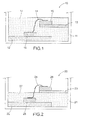
- the figure 1 represents an electronic box 10 intended to be embedded, for example, in a motor vehicle.
- the housing comprises a casing 11, for example made of aluminum, which contains two electronic boards 12 and 13.
- the electronic boards 12 and 13 (or PCBs for "Printing Circuit Board") are fixed to the casing 11 by unrepresented fastening means ( spacers, threaded rods and nuts, for example).
- the electronic card 12 is for example a power card and the electronic card 13 is a control card.
- the electronic card 12 is for example a power card and the electronic card 13 is a control card.
- We did not represent on the figure 1 for simplicity, only one electrical conductor 14 connecting between the two electronic cards 12 and 13 but there may be several.
- the housing 10 may contain more than two electronic cards, each card can be connected to another card by one or more electrical conductors.
- the electrical conductor 14 electrically connects an electrically conductive pad 15 of the electronic card 12 to an electrically conductive pad 16 of the electronic card 13.
- the ends of the electrical conductor 14 are welded to the pads 15 and 16 by the technique of bevel welding or "Wedge bonding".
- one or more electronic components of the electronic card 12 is or are connected to one or more electronic components of the electronic card 13.
- a coating resin 17 was cast and polymerized in the housing 11 so as to coat the two electronic boards.
- the welded ends of the electrical conductor 14 are protected from oxidation, thermal shock, vibration and wet heat.
- the figure 1 shows an embodiment of the invention where the electronic cards are completely coated with resin, which has the effect of also protecting the components on the electronic cards and the cards themselves which are subject in particular to vibration stresses.
- the protective resin could also be distributed only on one of the welded ends of the electrical conductor, or on both ends of this electrical conductor.
- the figure 2 represents a second example of implementation of the invention.
- the control unit 20 comprises a housing 21 containing two electronic boards 22 and 23.
- the electronic boards 22 and 23 are fixed to the casing 21 by unrepresented fastening means.
- the electronic card 22 is a power card and the electronic card 23 is a control card.
- the electrical conductor 24 electrically connects an electrically conductive pad 25 of the electronic card 22 to an electrically conductive pad 26 of the electronic card 23.
- the ends of the conductor electrical 24 are welded to the pads 25 and 26 by the technique of "wedge bonding".
- a coating resin 27 has been cast and polymerized in the housing 21 so as to coat only the electronic card 22.
- the polyurethane resin used to implement the present invention may be a resin marketed by SEG Dietticies and polymerizable at room temperature. It is thus possible to obtain electronic casings resistant to thermal shocks between -40 ° C and + 125 ° C and satisfying vibration tests for a vibration greater than 30 G.
- the polyurethane resin allows the evacuation of calories generated by the electronic power cards, at a rate of 0.4 W / m ° C, to the metal casing of the housing.
- the use of a polyurethane resin makes it possible to avoid the use of a polymerization oven.
- the electronic box shown at figure 1 where the electrical bonding conductor is completely encapsulated with resin has the advantage of not requiring a resin deposition robot and the assembly comprising a UV lamp and an optical fiber guide for the polymerization. The manufacturing cycle time is reduced.
- the price of the polyurethane resin is also advantageous. Thus, it is estimated that, for the example illustrated by figure 1 , 75% the cost of implementation with respect to an epoxy resin. In addition, the polyurethane resin promotes the evacuation of calories.
- the polyurethane resin is for example a material belonging to the Shore A hardness scale.
- the invention also relates to a power module comprising at least one power component.
- the power module includes a housing in which the power component is mounted and containing polyurethane resin to protect the component as described in the above electronic package.
- the power component is for example an electronic chip.
- the power component is electrically connected with an electrically conductive pad 15, 16, 25, 26 or with another power component by conductors 14 welded by the technique of "wedge bonding" as previously described.
- the electrical conductor 14 is welded to a respective solder area of the component.
- the conductor 14 and the solder pads of the components or the electrically conductive pads 15, 16, 25, 26 have characteristics making it possible to obtain a form of electrical conductor 14 improving its resistance in the polyurethane resin, especially its mechanical strength.
- the electrical conductor 14 has a bent shape in the vicinity of the conductive pad 15, 16, 25, 26 or the welding range.
- the conductor 14 is welded at both ends, and the horizontal distance between the two welds is greater than or equal to 6 mm.
- the vertical distance between the two welds can be less than or equal to 10 mm, and the length of the conductor 14 may be less than or equal to a value of 150xD where D is the diameter of the conductor 14.
- the conductor 14 has a diameter D of between 300 and 500 microns.
Landscapes
- Engineering & Computer Science (AREA)
- Microelectronics & Electronic Packaging (AREA)
- Manufacturing & Machinery (AREA)
- Casings For Electric Apparatus (AREA)
- Non-Metallic Protective Coatings For Printed Circuits (AREA)
- Combinations Of Printed Boards (AREA)
Abstract
Description
- L'invention se rapporte à un boîtier électronique destiné à être embarqué dans un véhicule, en particulier dans un véhicule automobile. Elle concerne tout assemblage de cartes électroniques ou PCB (pour « Printed-Circuit Board ») installées sur un carter métallique ou plastique (électronique de puissance, électronique de commande), dans un environnement mécatronique, électronique embarquée. Bien qu'une application particulière soit celle de l'automobile, l'invention peut s'appliquer à des domaines présentant des contraintes d'utilisation proches ou similaires.
- Actuellement les boîtiers électroniques embarqués dans une automobile sont soumis à des chocs thermiques et à des vibrations suivant les cahiers des charges respectifs de chaque constructeur. Pour respecter les exigences de qualité de chaque constructeur, les cartes électroniques équipées (puissance et commande) sont fixées dans des carters, leurs interconnexions étant assurées par différentes technologies, notamment celle appelée « wedge bonding ».
- La technique du « wedge bonding » se définit comme suit. Un fil, le plus souvent en aluminium est amené par un outil (appelé stylet ou aiguille), il est appliqué sur le plot à souder. La liaison entre le fil et la zone à connecter s'effectue en combinant pression et vibration ultrasonore. Il s'agit d'une soudure dite « à froid ». C'est l'énergie ultrasonique qui entraîne le ramollissement du fil, semblable à l'effet obtenu par une élévation de température. Le fil est ensuite guidé par l'outil sur le second plot et la soudure est effectuée. Les fils peuvent avoir des diamètres compris entre 75 µm et 650 µm.
- Pour protéger ces soudures contre l'oxydation, les chocs thermiques, les vibrations et la chaleur humide on utilise des résines à base époxy ou acrylique ou des gels de silicone. Les résines sont déposées localement à l'aide de distributeurs. Elles sont polymérisées soit au four, soit par UV. Les gels de silicone sont coulés dans des zones de rétention dans lesquelles sont soudés les fils de liaison (« bonding ») .
- Les résines époxy ou acryliques, ainsi que les gels de silicone, présentent de bonnes performances thermiques, d'isolation électrique et mécanique. Cependant, leur mise en oeuvre, pour les boîtiers électroniques embarqués est cause d'un coût de revient de ces boîtiers jugé excessif par les constructeurs automobiles notamment.
- Afin de remédier au problème de coût exposé ci-dessus, il est proposé de remplacer le matériau de protection des cartes électroniques disposées dans un carter (résine époxy, résine acrylique, gels de silicone) par une résine polyuréthane. La résine polyuréthane présente des performances thermiques, d'isolation électrique et mécanique équivalentes à celles des matériaux de l'art antérieur (résine époxy, résine acryline, gel de silicone), cependant le gain économique résultant du matériau et de sa mise en oeuvre est très important.
- De par ses propriétés mécaniques et son expansion thermique (220. 10-6 m/°C), l'invention s'applique avantageusement sur des fils d'aluminium de diamètre supérieur ou égal à 250 µm et sur des rubans d'aluminium.
- L'invention a donc pour objet un boîtier électronique destiné à être embarqué dans un véhicule, le boîtier comprenant un carter contenant au moins deux cartes électroniques reliées entre elles par au moins un conducteur électrique, le conducteur ayant l'une de ses extrémités soudée sur l'une des cartes électroniques et l'autre de ses extrémités soudée sur l'autre carte électronique, les extrémités du conducteur étant soudées par la technique du soudage en biseau ou « wedge bonding », le carter contenant en outre une résine de protection enrobant au moins l'une des extrémités soudées du conducteur électrique, caractérisé en ce que la résine est une résine polyuréthane.
- L'une des deux cartes électroniques peut être une carte de puissance, l'autre carte électronique peut être une carte de commande.
- Selon un premier mode de réalisation, la résine de protection enrobe complètement les cartes électroniques.
- Selon un deuxième mode de réalisation, la résine de protection n'enrobe que la carte électronique de puissance. Dans ce cas, la carte de commande peut reposer sur la résine d'enrobage.
- Le conducteur électrique peut être un fil d'aluminium de diamètre supérieur à 250 µm. Il peut s'agir aussi d'un ruban d'aluminium.
- Le carter peut avantageusement être en aluminium.
- L'invention sera mieux comprise et d'autres avantages et particularités apparaîtront à la lecture de la description qui va suivre, donnée à titre d'exemple non limitatif, accompagnée des dessins annexés parmi lesquels :
- la
figure 1 représente un premier mode de mise en oeuvre de l'invention pour un boîtier électronique comprenant une carte électronique de puissance et une carte électronique de commande, - la
figure 2 représente un deuxième mode de mise en oeuvre de l'invention pour un boîtier électronique comprenant une carte électronique de puissance et une carte électronique de commande. - La
figure 1 représente un boîtier électronique 10 destiné à être embarqué, à titre d'exemple, dans un véhicule automobile. Le boîtier comprend un carter 11, par exemple en aluminium, qui contient deux cartes électroniques 12 et 13. Les cartes électroniques 12 et 13 (ou PCB pour « Printing Circuit Board ») sont fixées au carter 11 par des moyens de fixation non représentés (entretoises, tiges filetées et écrous par exemple). - La carte électronique 12 est par exemple une carte de puissance et la carte électronique 13 est une carte de commande. On n'a représenté sur la
figure 1 , par souci de simplification, qu'un seul conducteur électrique 14 de liaison entre les deux cartes électroniques 12 et 13 mais il peut y en avoir plusieurs. De même, le boîtier 10 peut contenir plus de deux cartes électroniques, chaque carte pouvant être reliée à une autre carte par un ou plusieurs conducteurs électriques. - Le conducteur électrique 14 relie électriquement un plot électriquement conducteur 15 de la carte électronique 12 à un plot électriquement conducteur 16 de la carte électronique 13. Les extrémités du conducteur électrique 14 sont soudées sur les plots 15 et 16 par la technique du soudage en biseau ou « wedge bonding ». Ainsi, un ou plusieurs composants électroniques de la carte électronique 12 est ou sont connectés à un ou plusieurs composants électroniques de la carte électronique 13.
- Comme le montre la
figure 1 , une résine d'enrobage 17 a été coulée et polymérisée dans le carter 11 de manière à enrober les deux cartes électroniques. Ainsi les extrémités soudées du conducteur électrique 14 sont protégées de l'oxydation, des chocs thermiques, des vibrations et de la chaleur humide. - La
figure 1 montre un mode de réalisation de l'invention où les cartes électroniques sont complètement enrobées de résine, ce qui a pour effet de protéger également les composants situés sur les cartes électroniques et les cartes elles-mêmes qui sont soumises notamment à des contraintes de vibration. - La résine de protection pourrait aussi n'être distribuée que sur l'une des extrémités soudées du conducteur électrique, ou sur les deux extrémités de ce conducteur électrique.
- La
figure 2 représente un deuxième exemple de mise en oeuvre de l'invention. Dans cet exemple, le boîtier électronique 20 comprend un carter 21 contenant deux cartes électroniques 22 et 23. Comme dans l'exemple précédent, les cartes électroniques 22 et 23 sont fixées au carter 21 par des moyens de fixation non représentées. Comme précédemment aussi, la carte électronique 22 est une carte de puissance et la carte électronique 23 est une carte de commande. Le conducteur électrique 24 relie électriquement un plot électriquement conducteur 25 de la carte électronique 22 à un plot électriquement conducteur 26 de la carte électronique 23. Les extrémités du conducteur électrique 24 sont soudées sur les plots 25 et 26 par la technique du « wedge bonding ». - Dans le cas du boîtier illustré par la
figure 2 , une résine d'enrobage 27 a été coulée et polymérisée dans le carter 21 de manière à enrober seulement la carte électronique 22. - La résine polyuréthane utilisée pour mettre en oeuvre la présente invention peut être une résine commercialisée par la société SEG Diélectriques et polymérisable à température ambiante. On peut ainsi obtenir des boîtiers électroniques résistant à des chocs thermiques entre -40°C et +125°C et satisfaisants à des tests de vibration pour une vibration supérieure à 30 G.
- La résine polyuréthane permet l'évacuation de calories générées par les cartes électroniques de puissance, à raison de 0,4 W/m.°C, vers le carter métallique du boîtier.
- L'utilisation d'une résine polyuréthane permet d'éviter l'utilisation d'un four de polymérisation. Le boîtier électronique illustré à la
figure 1 , où le conducteur électrique de liaison est complètement enrobé de résine, présente l'avantage de ne pas nécessiter de robot de dépose de résine et de l'ensemble comprenant une lampe UV et un guide de fibres optiques pour la polymérisation. Le temps de cycle de fabrication est réduit. - Le prix de la résine polyuréthane est aussi avantageux. Ainsi, on estime diminuer, pour l'exemple illustré par la
figure 1 , de 75% le coût de mise en oeuvre par rapport à une résine époxy. En outre, la résine polyuréthane favorise l'évacuation des calories. - La résine polyuréthane est par exemple un matériau appartenant à l'échelle de dureté shore A.
- L'invention concerne également un module de puissance comprenant au moins un composant de puissance. Le module de puissance comprend un boîtier dans lequel le composant de puissance est monté et contenant de la résine polyuréthane pour protéger le composant tel que décrit dans le boîtier électronique ci-dessus. Le composant de puissance est par exemple une puce électronique. De préférence, le composant de puissance est relié électriquement avec un plot électriquement conducteur 15, 16, 25, 26 ou avec un autre composant de puissance par des conducteurs 14 soudés par la technique du « wedge bonding » tel que précédemment décrit. Le conducteur électrique 14 est soudé sur une plage de soudure respective du composant.
- Dans un mode de réalisation, le conducteur 14 et les plages de soudure des composants ou les plots électriquement conducteurs 15, 16, 25, 26 présentent des caractéristiques permettant d'obtenir une forme de conducteur électrique 14 améliorant sa tenue dans la résine polyuréthane, en particulier sa tenue mécanique. En particulier, le conducteur électrique 14 a une forme coudée au voisinage du plot conducteur 15, 16, 25, 26 ou de la plage de soudure.
- Par exemple, le conducteur 14 est soudé à ses deux extrémités, et la distance horizontale entre les deux soudures est supérieure ou égale à 6 mm. La distance verticale entre les deux soudures peut être inférieure ou égale à 10 mm, et la longueur du conducteur 14 peut être inférieure ou égale à une valeur de 150xD où D est le diamètre du conducteur 14. De préférence, le conducteur 14 a un diamètre D compris entre 300 et 500 µm. Ces caractéristiques améliorent la tenue du conducteur 14 dans la résine polyuréthane.
Claims (8)
- Boîtier électronique (10, 20) destiné à être embarqué dans un véhicule, le boîtier comprenant un carter (11, 21) contenant au moins deux cartes électroniques (12, 13 ; 22, 23) reliées entre elles par au moins un conducteur électrique (14, 24), le conducteur ayant l'une de ses extrémités soudée sur l'une des cartes électroniques et l'autre de ses extrémités soudée sur l'autre carte électronique, les extrémités du conducteur étant soudées par la technique du soudage en biseau ou « wedge bonding », le carter contenant en outre une résine de protection (17, 27) enrobant au moins l'une des extrémités soudées du conducteur électrique, caractérisé en ce que la résine de protection est une résine polyuréthane.
- Boîtier électronique selon la revendication 1, dans lequel l'une (12, 22) des deux cartes électroniques est une carte de puissance, l'autre carte électronique (13, 23) étant une carte de commande.
- Boîtier électronique selon la revendication 2, dans lequel la résine de protection (17) enrobe complètement les cartes électroniques (13, 23).
- Boîtier électronique selon la revendication 2, dans lequel la résine de protection (27) n'enrobe que la carte électronique de puissance (22) .
- Boîtier électronique selon la revendication 4, dans lequel la carte de commande (23) repose sur la résine d'enrobage (27).
- Boîtier électronique selon l'une quelconque des revendications 1 à 5, dans lequel le conducteur électrique (14, 24) est un fil d'aluminium de diamètre supérieur à 250 µm.
- Boîtier électronique selon l'une quelconque des revendications 1 à 5, dans lequel le conducteur électrique (14, 24) est un ruban d'aluminium.
- Boîtier électronique selon l'une quelconque des revendications 1 à 7, dans lequel le carter (11, 21) est en aluminium.
Applications Claiming Priority (1)
| Application Number | Priority Date | Filing Date | Title |
|---|---|---|---|
| FR1057648A FR2965447B1 (fr) | 2010-09-23 | 2010-09-23 | Boitier electronique pour vehicule |
Publications (2)
| Publication Number | Publication Date |
|---|---|
| EP2434849A1 true EP2434849A1 (fr) | 2012-03-28 |
| EP2434849B1 EP2434849B1 (fr) | 2015-12-02 |
Family
ID=43919955
Family Applications (1)
| Application Number | Title | Priority Date | Filing Date |
|---|---|---|---|
| EP11182445.4A Not-in-force EP2434849B1 (fr) | 2010-09-23 | 2011-09-23 | Boîtier électronique pour véhicule |
Country Status (7)
| Country | Link |
|---|---|
| US (1) | US9167709B2 (fr) |
| EP (1) | EP2434849B1 (fr) |
| JP (1) | JP6082180B2 (fr) |
| KR (1) | KR20120031262A (fr) |
| CN (1) | CN102573371B (fr) |
| BR (1) | BRPI1105443A2 (fr) |
| FR (1) | FR2965447B1 (fr) |
Cited By (1)
| Publication number | Priority date | Publication date | Assignee | Title |
|---|---|---|---|---|
| EP3809564A1 (fr) * | 2019-10-15 | 2021-04-21 | Baumüller Nürnberg GmbH | Entraînement |
Families Citing this family (1)
| Publication number | Priority date | Publication date | Assignee | Title |
|---|---|---|---|---|
| FR3086495B1 (fr) * | 2018-09-24 | 2023-01-20 | Valeo Vision | Connexion electrique pour un module d'eclairage a fonction dynamique d'un vehicule automobile |
Citations (3)
| Publication number | Priority date | Publication date | Assignee | Title |
|---|---|---|---|---|
| JP2003318568A (ja) * | 2002-04-23 | 2003-11-07 | Hitachi Unisia Automotive Ltd | 電子部品装置 |
| JP2009130230A (ja) * | 2007-11-27 | 2009-06-11 | Kyocera Corp | 電力制御モジュール |
| EP2120263A1 (fr) * | 2007-11-30 | 2009-11-18 | Panasonic Corporation | Plaque de base à structure de dissipation de chaleur, module utilisant une plaque de base à structure de dissipation de chaleur, et procédé de fabrication d'une plaque de base à structure de dissipation de chaleur |
Family Cites Families (6)
| Publication number | Priority date | Publication date | Assignee | Title |
|---|---|---|---|---|
| JP2912526B2 (ja) * | 1993-07-05 | 1999-06-28 | 三菱電機株式会社 | 半導体パワーモジュールおよび複合基板 |
| JP3646665B2 (ja) * | 2001-04-17 | 2005-05-11 | 株式会社日立製作所 | インバータ装置 |
| JP2004087735A (ja) * | 2002-08-26 | 2004-03-18 | Toshiba Corp | 半導体装置 |
| JP3882734B2 (ja) * | 2002-10-16 | 2007-02-21 | 富士電機デバイステクノロジー株式会社 | パワー半導体装置のワイヤボンディング方法 |
| US20060163315A1 (en) * | 2005-01-27 | 2006-07-27 | Delsman Mark A | Ribbon bonding tool and process |
| JP4954356B1 (ja) * | 2011-10-12 | 2012-06-13 | 日本碍子株式会社 | 大容量モジュールの周辺回路用の回路基板、及び当該回路基板を用いる周辺回路を含む大容量モジュール |
-
2010
- 2010-09-23 FR FR1057648A patent/FR2965447B1/fr not_active Expired - Fee Related
-
2011
- 2011-09-22 JP JP2011207205A patent/JP6082180B2/ja not_active Expired - Fee Related
- 2011-09-22 BR BRPI1105443-3A patent/BRPI1105443A2/pt not_active Application Discontinuation
- 2011-09-22 US US13/239,557 patent/US9167709B2/en not_active Expired - Fee Related
- 2011-09-23 CN CN201110384758.6A patent/CN102573371B/zh not_active Expired - Fee Related
- 2011-09-23 EP EP11182445.4A patent/EP2434849B1/fr not_active Not-in-force
- 2011-09-23 KR KR1020110096357A patent/KR20120031262A/ko not_active Withdrawn
Patent Citations (3)
| Publication number | Priority date | Publication date | Assignee | Title |
|---|---|---|---|---|
| JP2003318568A (ja) * | 2002-04-23 | 2003-11-07 | Hitachi Unisia Automotive Ltd | 電子部品装置 |
| JP2009130230A (ja) * | 2007-11-27 | 2009-06-11 | Kyocera Corp | 電力制御モジュール |
| EP2120263A1 (fr) * | 2007-11-30 | 2009-11-18 | Panasonic Corporation | Plaque de base à structure de dissipation de chaleur, module utilisant une plaque de base à structure de dissipation de chaleur, et procédé de fabrication d'une plaque de base à structure de dissipation de chaleur |
Cited By (2)
| Publication number | Priority date | Publication date | Assignee | Title |
|---|---|---|---|---|
| EP3809564A1 (fr) * | 2019-10-15 | 2021-04-21 | Baumüller Nürnberg GmbH | Entraînement |
| EP4440258A3 (fr) * | 2019-10-15 | 2024-12-18 | Baumüller Nürnberg GmbH | Entraînement |
Also Published As
| Publication number | Publication date |
|---|---|
| CN102573371A (zh) | 2012-07-11 |
| FR2965447A1 (fr) | 2012-03-30 |
| BRPI1105443A2 (pt) | 2013-02-19 |
| JP2012124459A (ja) | 2012-06-28 |
| FR2965447B1 (fr) | 2012-08-31 |
| US9167709B2 (en) | 2015-10-20 |
| KR20120031262A (ko) | 2012-04-02 |
| EP2434849B1 (fr) | 2015-12-02 |
| CN102573371B (zh) | 2016-06-01 |
| JP6082180B2 (ja) | 2017-02-15 |
| US20120075811A1 (en) | 2012-03-29 |
Similar Documents
| Publication | Publication Date | Title |
|---|---|---|
| US6521989B2 (en) | Methods and apparatus for hermetically sealing electronic packages | |
| CN100565943C (zh) | 光电元件 | |
| US20060001116A1 (en) | Semiconductor module with a semiconductor sensor chip and a plastic package as well as method for its production | |
| US20040150064A1 (en) | Optoelectronic component array and method for the production of an optoelectronic component array | |
| CN1249835A (zh) | 印刷电路板模件和包含该模件的印刷电路板 | |
| FR2910701A1 (fr) | Module de puce et son procede de production | |
| JP2008039571A (ja) | 電流センサ | |
| JP2007049152A (ja) | Ledパッケージ及びその製造方法 | |
| KR20160100972A (ko) | 전자 제어 모듈 및 전자 제어 모듈의 제조 방법 | |
| EP2434849B1 (fr) | Boîtier électronique pour véhicule | |
| US20070029668A1 (en) | Package module having a stacking platform | |
| CN106605297B (zh) | 模块装置以及变速器控制模块 | |
| US8664758B2 (en) | Semiconductor package having reliable electrical connection and assembling method | |
| JP2010071724A (ja) | 樹脂モールド半導体センサ及び製造方法 | |
| TWI291242B (en) | Optoelectronic module and its production method | |
| JP5571330B2 (ja) | レンズサポートおよびワイヤボンドプロテクタ | |
| US7135768B2 (en) | Hermetic seal | |
| EP3319115B1 (fr) | Procédé de réalisation d'une connexion électrique entre une puce électronique et une plaque de support et dispositif électronique | |
| US20080122073A1 (en) | MEMS module package | |
| EP3319114A1 (fr) | Procédé de réalisation d'une connexion électrique entre une puce électronique et une plaque de support et dispositif électronique | |
| EP1724712A1 (fr) | Micromodule, notamment pour carte à puce | |
| US20080061409A1 (en) | Micro electro-mechanical system module package | |
| CN219696443U (zh) | 基于点胶工艺的封装结构 | |
| WO2007148398A1 (fr) | Module scellé par résine, module optique et procédé de scellement par résine | |
| JP2005530019A (ja) | テープ製造方法 |
Legal Events
| Date | Code | Title | Description |
|---|---|---|---|
| PUAI | Public reference made under article 153(3) epc to a published international application that has entered the european phase |
Free format text: ORIGINAL CODE: 0009012 |
|
| AK | Designated contracting states |
Kind code of ref document: A1 Designated state(s): AL AT BE BG CH CY CZ DE DK EE ES FI FR GB GR HR HU IE IS IT LI LT LU LV MC MK MT NL NO PL PT RO RS SE SI SK SM TR |
|
| AX | Request for extension of the european patent |
Extension state: BA ME |
|
| 17P | Request for examination filed |
Effective date: 20120928 |
|
| GRAP | Despatch of communication of intention to grant a patent |
Free format text: ORIGINAL CODE: EPIDOSNIGR1 |
|
| INTG | Intention to grant announced |
Effective date: 20150526 |
|
| RIN1 | Information on inventor provided before grant (corrected) |
Inventor name: MORENO, JEAN-YVES Inventor name: SILVESTRE, BENEDICTE Inventor name: GOVINDASSAMY, VALERY |
|
| GRAS | Grant fee paid |
Free format text: ORIGINAL CODE: EPIDOSNIGR3 |
|
| GRAA | (expected) grant |
Free format text: ORIGINAL CODE: 0009210 |
|
| AK | Designated contracting states |
Kind code of ref document: B1 Designated state(s): AL AT BE BG CH CY CZ DE DK EE ES FI FR GB GR HR HU IE IS IT LI LT LU LV MC MK MT NL NO PL PT RO RS SE SI SK SM TR |
|
| REG | Reference to a national code |
Ref country code: GB Ref legal event code: FG4D Free format text: NOT ENGLISH |
|
| REG | Reference to a national code |
Ref country code: AT Ref legal event code: REF Ref document number: 764111 Country of ref document: AT Kind code of ref document: T Effective date: 20151215 Ref country code: CH Ref legal event code: EP |
|
| REG | Reference to a national code |
Ref country code: IE Ref legal event code: FG4D Free format text: LANGUAGE OF EP DOCUMENT: FRENCH |
|
| REG | Reference to a national code |
Ref country code: DE Ref legal event code: R096 Ref document number: 602011021770 Country of ref document: DE |
|
| REG | Reference to a national code |
Ref country code: NL Ref legal event code: MP Effective date: 20160302 |
|
| REG | Reference to a national code |
Ref country code: LT Ref legal event code: MG4D |
|
| REG | Reference to a national code |
Ref country code: AT Ref legal event code: MK05 Ref document number: 764111 Country of ref document: AT Kind code of ref document: T Effective date: 20151202 |
|
| PG25 | Lapsed in a contracting state [announced via postgrant information from national office to epo] |
Ref country code: LT Free format text: LAPSE BECAUSE OF FAILURE TO SUBMIT A TRANSLATION OF THE DESCRIPTION OR TO PAY THE FEE WITHIN THE PRESCRIBED TIME-LIMIT Effective date: 20151202 Ref country code: NO Free format text: LAPSE BECAUSE OF FAILURE TO SUBMIT A TRANSLATION OF THE DESCRIPTION OR TO PAY THE FEE WITHIN THE PRESCRIBED TIME-LIMIT Effective date: 20160302 Ref country code: ES Free format text: LAPSE BECAUSE OF FAILURE TO SUBMIT A TRANSLATION OF THE DESCRIPTION OR TO PAY THE FEE WITHIN THE PRESCRIBED TIME-LIMIT Effective date: 20151202 |
|
| PG25 | Lapsed in a contracting state [announced via postgrant information from national office to epo] |
Ref country code: RS Free format text: LAPSE BECAUSE OF FAILURE TO SUBMIT A TRANSLATION OF THE DESCRIPTION OR TO PAY THE FEE WITHIN THE PRESCRIBED TIME-LIMIT Effective date: 20151202 Ref country code: AT Free format text: LAPSE BECAUSE OF FAILURE TO SUBMIT A TRANSLATION OF THE DESCRIPTION OR TO PAY THE FEE WITHIN THE PRESCRIBED TIME-LIMIT Effective date: 20151202 Ref country code: FI Free format text: LAPSE BECAUSE OF FAILURE TO SUBMIT A TRANSLATION OF THE DESCRIPTION OR TO PAY THE FEE WITHIN THE PRESCRIBED TIME-LIMIT Effective date: 20151202 Ref country code: PL Free format text: LAPSE BECAUSE OF FAILURE TO SUBMIT A TRANSLATION OF THE DESCRIPTION OR TO PAY THE FEE WITHIN THE PRESCRIBED TIME-LIMIT Effective date: 20151202 Ref country code: LV Free format text: LAPSE BECAUSE OF FAILURE TO SUBMIT A TRANSLATION OF THE DESCRIPTION OR TO PAY THE FEE WITHIN THE PRESCRIBED TIME-LIMIT Effective date: 20151202 Ref country code: NL Free format text: LAPSE BECAUSE OF FAILURE TO SUBMIT A TRANSLATION OF THE DESCRIPTION OR TO PAY THE FEE WITHIN THE PRESCRIBED TIME-LIMIT Effective date: 20151202 Ref country code: GR Free format text: LAPSE BECAUSE OF FAILURE TO SUBMIT A TRANSLATION OF THE DESCRIPTION OR TO PAY THE FEE WITHIN THE PRESCRIBED TIME-LIMIT Effective date: 20160303 Ref country code: SE Free format text: LAPSE BECAUSE OF FAILURE TO SUBMIT A TRANSLATION OF THE DESCRIPTION OR TO PAY THE FEE WITHIN THE PRESCRIBED TIME-LIMIT Effective date: 20151202 |
|
| PG25 | Lapsed in a contracting state [announced via postgrant information from national office to epo] |
Ref country code: IS Free format text: LAPSE BECAUSE OF FAILURE TO SUBMIT A TRANSLATION OF THE DESCRIPTION OR TO PAY THE FEE WITHIN THE PRESCRIBED TIME-LIMIT Effective date: 20151202 |
|
| PG25 | Lapsed in a contracting state [announced via postgrant information from national office to epo] |
Ref country code: IT Free format text: LAPSE BECAUSE OF FAILURE TO SUBMIT A TRANSLATION OF THE DESCRIPTION OR TO PAY THE FEE WITHIN THE PRESCRIBED TIME-LIMIT Effective date: 20151202 Ref country code: CZ Free format text: LAPSE BECAUSE OF FAILURE TO SUBMIT A TRANSLATION OF THE DESCRIPTION OR TO PAY THE FEE WITHIN THE PRESCRIBED TIME-LIMIT Effective date: 20151202 |
|
| PG25 | Lapsed in a contracting state [announced via postgrant information from national office to epo] |
Ref country code: SK Free format text: LAPSE BECAUSE OF FAILURE TO SUBMIT A TRANSLATION OF THE DESCRIPTION OR TO PAY THE FEE WITHIN THE PRESCRIBED TIME-LIMIT Effective date: 20151202 Ref country code: IS Free format text: LAPSE BECAUSE OF FAILURE TO SUBMIT A TRANSLATION OF THE DESCRIPTION OR TO PAY THE FEE WITHIN THE PRESCRIBED TIME-LIMIT Effective date: 20160402 Ref country code: EE Free format text: LAPSE BECAUSE OF FAILURE TO SUBMIT A TRANSLATION OF THE DESCRIPTION OR TO PAY THE FEE WITHIN THE PRESCRIBED TIME-LIMIT Effective date: 20151202 Ref country code: SM Free format text: LAPSE BECAUSE OF FAILURE TO SUBMIT A TRANSLATION OF THE DESCRIPTION OR TO PAY THE FEE WITHIN THE PRESCRIBED TIME-LIMIT Effective date: 20151202 Ref country code: PT Free format text: LAPSE BECAUSE OF FAILURE TO SUBMIT A TRANSLATION OF THE DESCRIPTION OR TO PAY THE FEE WITHIN THE PRESCRIBED TIME-LIMIT Effective date: 20160404 Ref country code: RO Free format text: LAPSE BECAUSE OF FAILURE TO SUBMIT A TRANSLATION OF THE DESCRIPTION OR TO PAY THE FEE WITHIN THE PRESCRIBED TIME-LIMIT Effective date: 20151202 |
|
| REG | Reference to a national code |
Ref country code: DE Ref legal event code: R097 Ref document number: 602011021770 Country of ref document: DE |
|
| REG | Reference to a national code |
Ref country code: FR Ref legal event code: PLFP Year of fee payment: 6 |
|
| PLBE | No opposition filed within time limit |
Free format text: ORIGINAL CODE: 0009261 |
|
| STAA | Information on the status of an ep patent application or granted ep patent |
Free format text: STATUS: NO OPPOSITION FILED WITHIN TIME LIMIT |
|
| PG25 | Lapsed in a contracting state [announced via postgrant information from national office to epo] |
Ref country code: DK Free format text: LAPSE BECAUSE OF FAILURE TO SUBMIT A TRANSLATION OF THE DESCRIPTION OR TO PAY THE FEE WITHIN THE PRESCRIBED TIME-LIMIT Effective date: 20151202 |
|
| 26N | No opposition filed |
Effective date: 20160905 |
|
| PG25 | Lapsed in a contracting state [announced via postgrant information from national office to epo] |
Ref country code: SI Free format text: LAPSE BECAUSE OF FAILURE TO SUBMIT A TRANSLATION OF THE DESCRIPTION OR TO PAY THE FEE WITHIN THE PRESCRIBED TIME-LIMIT Effective date: 20151202 |
|
| PG25 | Lapsed in a contracting state [announced via postgrant information from national office to epo] |
Ref country code: BE Free format text: LAPSE BECAUSE OF NON-PAYMENT OF DUE FEES Effective date: 20160930 |
|
| PG25 | Lapsed in a contracting state [announced via postgrant information from national office to epo] |
Ref country code: MC Free format text: LAPSE BECAUSE OF FAILURE TO SUBMIT A TRANSLATION OF THE DESCRIPTION OR TO PAY THE FEE WITHIN THE PRESCRIBED TIME-LIMIT Effective date: 20151202 |
|
| REG | Reference to a national code |
Ref country code: CH Ref legal event code: PL |
|
| GBPC | Gb: european patent ceased through non-payment of renewal fee |
Effective date: 20160923 |
|
| REG | Reference to a national code |
Ref country code: IE Ref legal event code: MM4A |
|
| PG25 | Lapsed in a contracting state [announced via postgrant information from national office to epo] |
Ref country code: GB Free format text: LAPSE BECAUSE OF NON-PAYMENT OF DUE FEES Effective date: 20160923 Ref country code: CH Free format text: LAPSE BECAUSE OF NON-PAYMENT OF DUE FEES Effective date: 20160930 Ref country code: LI Free format text: LAPSE BECAUSE OF NON-PAYMENT OF DUE FEES Effective date: 20160930 Ref country code: IE Free format text: LAPSE BECAUSE OF NON-PAYMENT OF DUE FEES Effective date: 20160923 |
|
| PG25 | Lapsed in a contracting state [announced via postgrant information from national office to epo] |
Ref country code: LU Free format text: LAPSE BECAUSE OF NON-PAYMENT OF DUE FEES Effective date: 20160923 |
|
| REG | Reference to a national code |
Ref country code: FR Ref legal event code: PLFP Year of fee payment: 7 |
|
| REG | Reference to a national code |
Ref country code: BE Ref legal event code: MM Effective date: 20160930 |
|
| PG25 | Lapsed in a contracting state [announced via postgrant information from national office to epo] |
Ref country code: CY Free format text: LAPSE BECAUSE OF FAILURE TO SUBMIT A TRANSLATION OF THE DESCRIPTION OR TO PAY THE FEE WITHIN THE PRESCRIBED TIME-LIMIT Effective date: 20151202 Ref country code: HU Free format text: LAPSE BECAUSE OF FAILURE TO SUBMIT A TRANSLATION OF THE DESCRIPTION OR TO PAY THE FEE WITHIN THE PRESCRIBED TIME-LIMIT; INVALID AB INITIO Effective date: 20110923 |
|
| PG25 | Lapsed in a contracting state [announced via postgrant information from national office to epo] |
Ref country code: HR Free format text: LAPSE BECAUSE OF FAILURE TO SUBMIT A TRANSLATION OF THE DESCRIPTION OR TO PAY THE FEE WITHIN THE PRESCRIBED TIME-LIMIT Effective date: 20151202 Ref country code: MK Free format text: LAPSE BECAUSE OF FAILURE TO SUBMIT A TRANSLATION OF THE DESCRIPTION OR TO PAY THE FEE WITHIN THE PRESCRIBED TIME-LIMIT Effective date: 20151202 Ref country code: TR Free format text: LAPSE BECAUSE OF FAILURE TO SUBMIT A TRANSLATION OF THE DESCRIPTION OR TO PAY THE FEE WITHIN THE PRESCRIBED TIME-LIMIT Effective date: 20151202 Ref country code: MT Free format text: LAPSE BECAUSE OF FAILURE TO SUBMIT A TRANSLATION OF THE DESCRIPTION OR TO PAY THE FEE WITHIN THE PRESCRIBED TIME-LIMIT Effective date: 20151202 |
|
| PG25 | Lapsed in a contracting state [announced via postgrant information from national office to epo] |
Ref country code: BG Free format text: LAPSE BECAUSE OF FAILURE TO SUBMIT A TRANSLATION OF THE DESCRIPTION OR TO PAY THE FEE WITHIN THE PRESCRIBED TIME-LIMIT Effective date: 20151202 |
|
| REG | Reference to a national code |
Ref country code: FR Ref legal event code: PLFP Year of fee payment: 8 |
|
| PG25 | Lapsed in a contracting state [announced via postgrant information from national office to epo] |
Ref country code: AL Free format text: LAPSE BECAUSE OF FAILURE TO SUBMIT A TRANSLATION OF THE DESCRIPTION OR TO PAY THE FEE WITHIN THE PRESCRIBED TIME-LIMIT Effective date: 20151202 |
|
| PGFP | Annual fee paid to national office [announced via postgrant information from national office to epo] |
Ref country code: FR Payment date: 20210930 Year of fee payment: 11 |
|
| PGFP | Annual fee paid to national office [announced via postgrant information from national office to epo] |
Ref country code: DE Payment date: 20210908 Year of fee payment: 11 |
|
| REG | Reference to a national code |
Ref country code: DE Ref legal event code: R119 Ref document number: 602011021770 Country of ref document: DE |
|
| PG25 | Lapsed in a contracting state [announced via postgrant information from national office to epo] |
Ref country code: FR Free format text: LAPSE BECAUSE OF NON-PAYMENT OF DUE FEES Effective date: 20220930 Ref country code: DE Free format text: LAPSE BECAUSE OF NON-PAYMENT OF DUE FEES Effective date: 20230401 |