EP2432039B1 - Light-emitting device and lighting device - Google Patents
Light-emitting device and lighting device Download PDFInfo
- Publication number
- EP2432039B1 EP2432039B1 EP11181085.9A EP11181085A EP2432039B1 EP 2432039 B1 EP2432039 B1 EP 2432039B1 EP 11181085 A EP11181085 A EP 11181085A EP 2432039 B1 EP2432039 B1 EP 2432039B1
- Authority
- EP
- European Patent Office
- Prior art keywords
- light
- emitting
- layer
- abbreviation
- refractive index
- Prior art date
- Legal status (The legal status is an assumption and is not a legal conclusion. Google has not performed a legal analysis and makes no representation as to the accuracy of the status listed.)
- Not-in-force
Links
- 239000000758 substrate Substances 0.000 claims description 56
- 239000007787 solid Substances 0.000 claims description 45
- 239000007788 liquid Substances 0.000 claims description 32
- 150000002894 organic compounds Chemical class 0.000 claims description 18
- 239000000853 adhesive Substances 0.000 claims description 3
- 230000001070 adhesive effect Effects 0.000 claims description 3
- 239000010410 layer Substances 0.000 description 208
- 239000000126 substance Substances 0.000 description 78
- 238000002347 injection Methods 0.000 description 52
- 239000007924 injection Substances 0.000 description 52
- 239000000463 material Substances 0.000 description 51
- -1 aromatic amine compounds Chemical class 0.000 description 32
- 230000005525 hole transport Effects 0.000 description 29
- CUJRVFIICFDLGR-UHFFFAOYSA-N acetylacetonate Chemical compound CC(=O)[CH-]C(C)=O CUJRVFIICFDLGR-UHFFFAOYSA-N 0.000 description 26
- 239000002131 composite material Substances 0.000 description 23
- 150000001875 compounds Chemical class 0.000 description 18
- 238000000034 method Methods 0.000 description 16
- IEQIEDJGQAUEQZ-UHFFFAOYSA-N phthalocyanine Chemical compound N1C(N=C2C3=CC=CC=C3C(N=C3C4=CC=CC=C4C(=N4)N3)=N2)=C(C=CC=C2)C2=C1N=C1C2=CC=CC=C2C4=N1 IEQIEDJGQAUEQZ-UHFFFAOYSA-N 0.000 description 14
- 238000000605 extraction Methods 0.000 description 12
- MILUBEOXRNEUHS-UHFFFAOYSA-N iridium(3+) Chemical compound [Ir+3] MILUBEOXRNEUHS-UHFFFAOYSA-N 0.000 description 12
- 229910052799 carbon Inorganic materials 0.000 description 11
- AZFHXIBNMPIGOD-UHFFFAOYSA-N 4-hydroxypent-3-en-2-one iridium Chemical compound [Ir].CC(O)=CC(C)=O.CC(O)=CC(C)=O.CC(O)=CC(C)=O AZFHXIBNMPIGOD-UHFFFAOYSA-N 0.000 description 10
- 238000004768 lowest unoccupied molecular orbital Methods 0.000 description 10
- DHDHJYNTEFLIHY-UHFFFAOYSA-N 4,7-diphenyl-1,10-phenanthroline Chemical compound C1=CC=CC=C1C1=CC=NC2=C1C=CC1=C(C=3C=CC=CC=3)C=CN=C21 DHDHJYNTEFLIHY-UHFFFAOYSA-N 0.000 description 9
- BVKZGUZCCUSVTD-UHFFFAOYSA-L Carbonate Chemical compound [O-]C([O-])=O BVKZGUZCCUSVTD-UHFFFAOYSA-L 0.000 description 9
- YXFVVABEGXRONW-UHFFFAOYSA-N Toluene Chemical compound CC1=CC=CC=C1 YXFVVABEGXRONW-UHFFFAOYSA-N 0.000 description 9
- 239000007983 Tris buffer Substances 0.000 description 9
- 150000004696 coordination complex Chemical class 0.000 description 9
- 150000004820 halides Chemical class 0.000 description 9
- 125000005595 acetylacetonate group Chemical group 0.000 description 8
- 229910052782 aluminium Inorganic materials 0.000 description 8
- XAGFODPZIPBFFR-UHFFFAOYSA-N aluminium Chemical compound [Al] XAGFODPZIPBFFR-UHFFFAOYSA-N 0.000 description 8
- 239000000872 buffer Substances 0.000 description 8
- 238000001704 evaporation Methods 0.000 description 8
- 239000011521 glass Substances 0.000 description 8
- 239000001301 oxygen Substances 0.000 description 8
- 229910052760 oxygen Inorganic materials 0.000 description 8
- 239000003086 colorant Substances 0.000 description 7
- XCJYREBRNVKWGJ-UHFFFAOYSA-N copper(II) phthalocyanine Chemical compound [Cu+2].C12=CC=CC=C2C(N=C2[N-]C(C3=CC=CC=C32)=N2)=NC1=NC([C]1C=CC=CC1=1)=NC=1N=C1[C]3C=CC=CC3=C2[N-]1 XCJYREBRNVKWGJ-UHFFFAOYSA-N 0.000 description 7
- 229910052751 metal Inorganic materials 0.000 description 7
- 239000002184 metal Substances 0.000 description 7
- JKQOBWVOAYFWKG-UHFFFAOYSA-N molybdenum trioxide Chemical compound O=[Mo](=O)=O JKQOBWVOAYFWKG-UHFFFAOYSA-N 0.000 description 7
- 239000011347 resin Substances 0.000 description 7
- 229920005989 resin Polymers 0.000 description 7
- ODHXBMXNKOYIBV-UHFFFAOYSA-N triphenylamine Chemical compound C1=CC=CC=C1N(C=1C=CC=CC=1)C1=CC=CC=C1 ODHXBMXNKOYIBV-UHFFFAOYSA-N 0.000 description 7
- LFQSCWFLJHTTHZ-UHFFFAOYSA-N Ethanol Chemical compound CCO LFQSCWFLJHTTHZ-UHFFFAOYSA-N 0.000 description 6
- XEEYBQQBJWHFJM-UHFFFAOYSA-N Iron Chemical compound [Fe] XEEYBQQBJWHFJM-UHFFFAOYSA-N 0.000 description 6
- PXHVJJICTQNCMI-UHFFFAOYSA-N Nickel Chemical compound [Ni] PXHVJJICTQNCMI-UHFFFAOYSA-N 0.000 description 6
- XLOMVQKBTHCTTD-UHFFFAOYSA-N Zinc monoxide Chemical compound [Zn]=O XLOMVQKBTHCTTD-UHFFFAOYSA-N 0.000 description 6
- 229910052757 nitrogen Inorganic materials 0.000 description 6
- RYGMFSIKBFXOCR-UHFFFAOYSA-N Copper Chemical compound [Cu] RYGMFSIKBFXOCR-UHFFFAOYSA-N 0.000 description 5
- 229910045601 alloy Inorganic materials 0.000 description 5
- 239000000956 alloy Substances 0.000 description 5
- 230000015572 biosynthetic process Effects 0.000 description 5
- 239000010949 copper Substances 0.000 description 5
- 230000008020 evaporation Effects 0.000 description 5
- PQXKHYXIUOZZFA-UHFFFAOYSA-M lithium fluoride Chemical compound [Li+].[F-] PQXKHYXIUOZZFA-UHFFFAOYSA-M 0.000 description 5
- 229910000476 molybdenum oxide Inorganic materials 0.000 description 5
- 229910052761 rare earth metal Inorganic materials 0.000 description 5
- STTGYIUESPWXOW-UHFFFAOYSA-N 2,9-dimethyl-4,7-diphenyl-1,10-phenanthroline Chemical compound C=12C=CC3=C(C=4C=CC=CC=4)C=C(C)N=C3C2=NC(C)=CC=1C1=CC=CC=C1 STTGYIUESPWXOW-UHFFFAOYSA-N 0.000 description 4
- FQJQNLKWTRGIEB-UHFFFAOYSA-N 2-(4-tert-butylphenyl)-5-[3-[5-(4-tert-butylphenyl)-1,3,4-oxadiazol-2-yl]phenyl]-1,3,4-oxadiazole Chemical compound C1=CC(C(C)(C)C)=CC=C1C1=NN=C(C=2C=C(C=CC=2)C=2OC(=NN=2)C=2C=CC(=CC=2)C(C)(C)C)O1 FQJQNLKWTRGIEB-UHFFFAOYSA-N 0.000 description 4
- ZVFQEOPUXVPSLB-UHFFFAOYSA-N 3-(4-tert-butylphenyl)-4-phenyl-5-(4-phenylphenyl)-1,2,4-triazole Chemical compound C1=CC(C(C)(C)C)=CC=C1C(N1C=2C=CC=CC=2)=NN=C1C1=CC=C(C=2C=CC=CC=2)C=C1 ZVFQEOPUXVPSLB-UHFFFAOYSA-N 0.000 description 4
- KDLHZDBZIXYQEI-UHFFFAOYSA-N Palladium Chemical compound [Pd] KDLHZDBZIXYQEI-UHFFFAOYSA-N 0.000 description 4
- NINIDFKCEFEMDL-UHFFFAOYSA-N Sulfur Chemical compound [S] NINIDFKCEFEMDL-UHFFFAOYSA-N 0.000 description 4
- 229910052783 alkali metal Inorganic materials 0.000 description 4
- 150000001340 alkali metals Chemical class 0.000 description 4
- 229910052784 alkaline earth metal Inorganic materials 0.000 description 4
- 150000001342 alkaline earth metals Chemical class 0.000 description 4
- 150000001491 aromatic compounds Chemical class 0.000 description 4
- 125000003118 aryl group Chemical group 0.000 description 4
- 230000000295 complement effect Effects 0.000 description 4
- AMWRITDGCCNYAT-UHFFFAOYSA-L hydroxy(oxo)manganese;manganese Chemical compound [Mn].O[Mn]=O.O[Mn]=O AMWRITDGCCNYAT-UHFFFAOYSA-L 0.000 description 4
- 239000003446 ligand Substances 0.000 description 4
- FUJCRWPEOMXPAD-UHFFFAOYSA-N lithium oxide Chemical compound [Li+].[Li+].[O-2] FUJCRWPEOMXPAD-UHFFFAOYSA-N 0.000 description 4
- 229910001947 lithium oxide Inorganic materials 0.000 description 4
- 239000007769 metal material Substances 0.000 description 4
- 239000000203 mixture Substances 0.000 description 4
- QJGQUHMNIGDVPM-UHFFFAOYSA-N nitrogen group Chemical group [N] QJGQUHMNIGDVPM-UHFFFAOYSA-N 0.000 description 4
- 125000001997 phenyl group Chemical group [H]C1=C([H])C([H])=C(*)C([H])=C1[H] 0.000 description 4
- BASFCYQUMIYNBI-UHFFFAOYSA-N platinum Chemical compound [Pt] BASFCYQUMIYNBI-UHFFFAOYSA-N 0.000 description 4
- 229920003227 poly(N-vinyl carbazole) Polymers 0.000 description 4
- 239000000843 powder Substances 0.000 description 4
- 150000002909 rare earth metal compounds Chemical class 0.000 description 4
- 150000002910 rare earth metals Chemical class 0.000 description 4
- 229910052717 sulfur Inorganic materials 0.000 description 4
- 239000011593 sulfur Substances 0.000 description 4
- 238000007738 vacuum evaporation Methods 0.000 description 4
- IYZMXHQDXZKNCY-UHFFFAOYSA-N 1-n,1-n-diphenyl-4-n,4-n-bis[4-(n-phenylanilino)phenyl]benzene-1,4-diamine Chemical compound C1=CC=CC=C1N(C=1C=CC(=CC=1)N(C=1C=CC(=CC=1)N(C=1C=CC=CC=1)C=1C=CC=CC=1)C=1C=CC(=CC=1)N(C=1C=CC=CC=1)C=1C=CC=CC=1)C1=CC=CC=C1 IYZMXHQDXZKNCY-UHFFFAOYSA-N 0.000 description 3
- MKAQNAJLIITRHR-UHFFFAOYSA-N 3-(3-dibenzothiophen-4-ylphenyl)phenanthro[9,10-b]pyrazine Chemical compound C1=CC=C2C3=NC(C=4C=CC=C(C=4)C4=C5SC=6C(C5=CC=C4)=CC=CC=6)=CN=C3C3=CC=CC=C3C2=C1 MKAQNAJLIITRHR-UHFFFAOYSA-N 0.000 description 3
- VFUDMQLBKNMONU-UHFFFAOYSA-N 9-[4-(4-carbazol-9-ylphenyl)phenyl]carbazole Chemical group C12=CC=CC=C2C2=CC=CC=C2N1C1=CC=C(C=2C=CC(=CC=2)N2C3=CC=CC=C3C3=CC=CC=C32)C=C1 VFUDMQLBKNMONU-UHFFFAOYSA-N 0.000 description 3
- 229910000838 Al alloy Inorganic materials 0.000 description 3
- 229910015711 MoOx Inorganic materials 0.000 description 3
- YNPNZTXNASCQKK-UHFFFAOYSA-N Phenanthrene Natural products C1=CC=C2C3=CC=CC=C3C=CC2=C1 YNPNZTXNASCQKK-UHFFFAOYSA-N 0.000 description 3
- GWEVSGVZZGPLCZ-UHFFFAOYSA-N Titan oxide Chemical compound O=[Ti]=O GWEVSGVZZGPLCZ-UHFFFAOYSA-N 0.000 description 3
- RTAQQCXQSZGOHL-UHFFFAOYSA-N Titanium Chemical compound [Ti] RTAQQCXQSZGOHL-UHFFFAOYSA-N 0.000 description 3
- HCHKCACWOHOZIP-UHFFFAOYSA-N Zinc Chemical compound [Zn] HCHKCACWOHOZIP-UHFFFAOYSA-N 0.000 description 3
- DGEZNRSVGBDHLK-UHFFFAOYSA-N [1,10]phenanthroline Chemical compound C1=CN=C2C3=NC=CC=C3C=CC2=C1 DGEZNRSVGBDHLK-UHFFFAOYSA-N 0.000 description 3
- 150000001339 alkali metal compounds Chemical class 0.000 description 3
- 150000001341 alkaline earth metal compounds Chemical class 0.000 description 3
- 150000004945 aromatic hydrocarbons Chemical class 0.000 description 3
- GQVWHWAWLPCBHB-UHFFFAOYSA-L beryllium;benzo[h]quinolin-10-olate Chemical compound [Be+2].C1=CC=NC2=C3C([O-])=CC=CC3=CC=C21.C1=CC=NC2=C3C([O-])=CC=CC3=CC=C21 GQVWHWAWLPCBHB-UHFFFAOYSA-L 0.000 description 3
- FJDQFPXHSGXQBY-UHFFFAOYSA-L caesium carbonate Chemical compound [Cs+].[Cs+].[O-]C([O-])=O FJDQFPXHSGXQBY-UHFFFAOYSA-L 0.000 description 3
- 229910000024 caesium carbonate Inorganic materials 0.000 description 3
- 150000001716 carbazoles Chemical class 0.000 description 3
- 230000003197 catalytic effect Effects 0.000 description 3
- 229910052802 copper Inorganic materials 0.000 description 3
- 238000002425 crystallisation Methods 0.000 description 3
- 230000008025 crystallization Effects 0.000 description 3
- NZZFYRREKKOMAT-UHFFFAOYSA-N diiodomethane Chemical compound ICI NZZFYRREKKOMAT-UHFFFAOYSA-N 0.000 description 3
- PJXISJQVUVHSOJ-UHFFFAOYSA-N indium(iii) oxide Chemical compound [O-2].[O-2].[O-2].[In+3].[In+3] PJXISJQVUVHSOJ-UHFFFAOYSA-N 0.000 description 3
- 229910052742 iron Inorganic materials 0.000 description 3
- XGZVUEUWXADBQD-UHFFFAOYSA-L lithium carbonate Chemical compound [Li+].[Li+].[O-]C([O-])=O XGZVUEUWXADBQD-UHFFFAOYSA-L 0.000 description 3
- 229910052808 lithium carbonate Inorganic materials 0.000 description 3
- 238000004519 manufacturing process Methods 0.000 description 3
- 229910044991 metal oxide Inorganic materials 0.000 description 3
- 150000004706 metal oxides Chemical class 0.000 description 3
- IBHBKWKFFTZAHE-UHFFFAOYSA-N n-[4-[4-(n-naphthalen-1-ylanilino)phenyl]phenyl]-n-phenylnaphthalen-1-amine Chemical group C1=CC=CC=C1N(C=1C2=CC=CC=C2C=CC=1)C1=CC=C(C=2C=CC(=CC=2)N(C=2C=CC=CC=2)C=2C3=CC=CC=C3C=CC=2)C=C1 IBHBKWKFFTZAHE-UHFFFAOYSA-N 0.000 description 3
- 229910052759 nickel Inorganic materials 0.000 description 3
- IJGRMHOSHXDMSA-UHFFFAOYSA-N nitrogen Substances N#N IJGRMHOSHXDMSA-UHFFFAOYSA-N 0.000 description 3
- PQQKPALAQIIWST-UHFFFAOYSA-N oxomolybdenum Chemical compound [Mo]=O PQQKPALAQIIWST-UHFFFAOYSA-N 0.000 description 3
- NFHFRUOZVGFOOS-UHFFFAOYSA-N palladium;triphenylphosphane Chemical compound [Pd].C1=CC=CC=C1P(C=1C=CC=CC=1)C1=CC=CC=C1.C1=CC=CC=C1P(C=1C=CC=CC=1)C1=CC=CC=C1.C1=CC=CC=C1P(C=1C=CC=CC=1)C1=CC=CC=C1.C1=CC=CC=C1P(C=1C=CC=CC=1)C1=CC=CC=C1 NFHFRUOZVGFOOS-UHFFFAOYSA-N 0.000 description 3
- 125000002080 perylenyl group Chemical group C1(=CC=C2C=CC=C3C4=CC=CC5=CC=CC(C1=C23)=C45)* 0.000 description 3
- 125000000951 phenoxy group Chemical group [H]C1=C([H])C([H])=C(O*)C([H])=C1[H] 0.000 description 3
- 230000009467 reduction Effects 0.000 description 3
- YYMBJDOZVAITBP-UHFFFAOYSA-N rubrene Chemical compound C1=CC=CC=C1C(C1=C(C=2C=CC=CC=2)C2=CC=CC=C2C(C=2C=CC=CC=2)=C11)=C(C=CC=C2)C2=C1C1=CC=CC=C1 YYMBJDOZVAITBP-UHFFFAOYSA-N 0.000 description 3
- 238000003786 synthesis reaction Methods 0.000 description 3
- XOLBLPGZBRYERU-UHFFFAOYSA-N tin dioxide Chemical compound O=[Sn]=O XOLBLPGZBRYERU-UHFFFAOYSA-N 0.000 description 3
- 229910052719 titanium Inorganic materials 0.000 description 3
- 239000010936 titanium Substances 0.000 description 3
- OGIDPMRJRNCKJF-UHFFFAOYSA-N titanium oxide Inorganic materials [Ti]=O OGIDPMRJRNCKJF-UHFFFAOYSA-N 0.000 description 3
- 239000011701 zinc Substances 0.000 description 3
- 229910052725 zinc Inorganic materials 0.000 description 3
- 239000011787 zinc oxide Substances 0.000 description 3
- UHXOHPVVEHBKKT-UHFFFAOYSA-N 1-(2,2-diphenylethenyl)-4-[4-(2,2-diphenylethenyl)phenyl]benzene Chemical group C=1C=C(C=2C=CC(C=C(C=3C=CC=CC=3)C=3C=CC=CC=3)=CC=2)C=CC=1C=C(C=1C=CC=CC=1)C1=CC=CC=C1 UHXOHPVVEHBKKT-UHFFFAOYSA-N 0.000 description 2
- HDMYKJVSQIHZLM-UHFFFAOYSA-N 1-[3,5-di(pyren-1-yl)phenyl]pyrene Chemical compound C1=CC(C=2C=C(C=C(C=2)C=2C3=CC=C4C=CC=C5C=CC(C3=C54)=CC=2)C=2C3=CC=C4C=CC=C5C=CC(C3=C54)=CC=2)=C2C=CC3=CC=CC4=CC=C1C2=C43 HDMYKJVSQIHZLM-UHFFFAOYSA-N 0.000 description 2
- SPDPTFAJSFKAMT-UHFFFAOYSA-N 1-n-[4-[4-(n-[4-(3-methyl-n-(3-methylphenyl)anilino)phenyl]anilino)phenyl]phenyl]-4-n,4-n-bis(3-methylphenyl)-1-n-phenylbenzene-1,4-diamine Chemical compound CC1=CC=CC(N(C=2C=CC(=CC=2)N(C=2C=CC=CC=2)C=2C=CC(=CC=2)C=2C=CC(=CC=2)N(C=2C=CC=CC=2)C=2C=CC(=CC=2)N(C=2C=C(C)C=CC=2)C=2C=C(C)C=CC=2)C=2C=C(C)C=CC=2)=C1 SPDPTFAJSFKAMT-UHFFFAOYSA-N 0.000 description 2
- 238000005160 1H NMR spectroscopy Methods 0.000 description 2
- XANIFASCQKHXRC-UHFFFAOYSA-N 2-(1,3-benzothiazol-2-yl)phenol zinc Chemical compound [Zn].Oc1ccccc1-c1nc2ccccc2s1.Oc1ccccc1-c1nc2ccccc2s1 XANIFASCQKHXRC-UHFFFAOYSA-N 0.000 description 2
- UOCMXZLNHQBBOS-UHFFFAOYSA-N 2-(1,3-benzoxazol-2-yl)phenol zinc Chemical compound [Zn].Oc1ccccc1-c1nc2ccccc2o1.Oc1ccccc1-c1nc2ccccc2o1 UOCMXZLNHQBBOS-UHFFFAOYSA-N 0.000 description 2
- GEQBRULPNIVQPP-UHFFFAOYSA-N 2-[3,5-bis(1-phenylbenzimidazol-2-yl)phenyl]-1-phenylbenzimidazole Chemical compound C1=CC=CC=C1N1C2=CC=CC=C2N=C1C1=CC(C=2N(C3=CC=CC=C3N=2)C=2C=CC=CC=2)=CC(C=2N(C3=CC=CC=C3N=2)C=2C=CC=CC=2)=C1 GEQBRULPNIVQPP-UHFFFAOYSA-N 0.000 description 2
- IXHWGNYCZPISET-UHFFFAOYSA-N 2-[4-(dicyanomethylidene)-2,3,5,6-tetrafluorocyclohexa-2,5-dien-1-ylidene]propanedinitrile Chemical compound FC1=C(F)C(=C(C#N)C#N)C(F)=C(F)C1=C(C#N)C#N IXHWGNYCZPISET-UHFFFAOYSA-N 0.000 description 2
- OBAJPWYDYFEBTF-UHFFFAOYSA-N 2-tert-butyl-9,10-dinaphthalen-2-ylanthracene Chemical compound C1=CC=CC2=CC(C3=C4C=CC=CC4=C(C=4C=C5C=CC=CC5=CC=4)C4=CC=C(C=C43)C(C)(C)C)=CC=C21 OBAJPWYDYFEBTF-UHFFFAOYSA-N 0.000 description 2
- USIXUMGAHVBSHQ-UHFFFAOYSA-N 9,10-bis(3,5-diphenylphenyl)anthracene Chemical compound C1=CC=CC=C1C1=CC(C=2C=CC=CC=2)=CC(C=2C3=CC=CC=C3C(C=3C=C(C=C(C=3)C=3C=CC=CC=3)C=3C=CC=CC=3)=C3C=CC=CC3=2)=C1 USIXUMGAHVBSHQ-UHFFFAOYSA-N 0.000 description 2
- VIZUPBYFLORCRA-UHFFFAOYSA-N 9,10-dinaphthalen-2-ylanthracene Chemical compound C12=CC=CC=C2C(C2=CC3=CC=CC=C3C=C2)=C(C=CC=C2)C2=C1C1=CC=C(C=CC=C2)C2=C1 VIZUPBYFLORCRA-UHFFFAOYSA-N 0.000 description 2
- FCNCGHJSNVOIKE-UHFFFAOYSA-N 9,10-diphenylanthracene Chemical compound C1=CC=CC=C1C(C1=CC=CC=C11)=C(C=CC=C2)C2=C1C1=CC=CC=C1 FCNCGHJSNVOIKE-UHFFFAOYSA-N 0.000 description 2
- UQVFZEYHQJJGPD-UHFFFAOYSA-N 9-[4-(10-phenylanthracen-9-yl)phenyl]carbazole Chemical compound C1=CC=CC=C1C(C1=CC=CC=C11)=C(C=CC=C2)C2=C1C1=CC=C(N2C3=CC=CC=C3C3=CC=CC=C32)C=C1 UQVFZEYHQJJGPD-UHFFFAOYSA-N 0.000 description 2
- SXGIRTCIFPJUEQ-UHFFFAOYSA-N 9-anthracen-9-ylanthracene Chemical group C1=CC=CC2=CC3=CC=CC=C3C(C=3C4=CC=CC=C4C=C4C=CC=CC4=3)=C21 SXGIRTCIFPJUEQ-UHFFFAOYSA-N 0.000 description 2
- DDCOSPFEMPUOFY-UHFFFAOYSA-N 9-phenyl-3-[4-(10-phenylanthracen-9-yl)phenyl]carbazole Chemical compound C1=CC=CC=C1C(C1=CC=CC=C11)=C(C=CC=C2)C2=C1C1=CC=C(C=2C=C3C4=CC=CC=C4N(C=4C=CC=CC=4)C3=CC=2)C=C1 DDCOSPFEMPUOFY-UHFFFAOYSA-N 0.000 description 2
- CSCPPACGZOOCGX-UHFFFAOYSA-N Acetone Chemical compound CC(C)=O CSCPPACGZOOCGX-UHFFFAOYSA-N 0.000 description 2
- 229910001316 Ag alloy Inorganic materials 0.000 description 2
- XKRFYHLGVUSROY-UHFFFAOYSA-N Argon Chemical compound [Ar] XKRFYHLGVUSROY-UHFFFAOYSA-N 0.000 description 2
- VYZAMTAEIAYCRO-UHFFFAOYSA-N Chromium Chemical compound [Cr] VYZAMTAEIAYCRO-UHFFFAOYSA-N 0.000 description 2
- 229910000881 Cu alloy Inorganic materials 0.000 description 2
- 229910052693 Europium Inorganic materials 0.000 description 2
- 229910000846 In alloy Inorganic materials 0.000 description 2
- ZOKXTWBITQBERF-UHFFFAOYSA-N Molybdenum Chemical compound [Mo] ZOKXTWBITQBERF-UHFFFAOYSA-N 0.000 description 2
- 238000005481 NMR spectroscopy Methods 0.000 description 2
- 229920001609 Poly(3,4-ethylenedioxythiophene) Polymers 0.000 description 2
- VYPSYNLAJGMNEJ-UHFFFAOYSA-N Silicium dioxide Chemical compound O=[Si]=O VYPSYNLAJGMNEJ-UHFFFAOYSA-N 0.000 description 2
- HEDRZPFGACZZDS-MICDWDOJSA-N Trichloro(2H)methane Chemical compound [2H]C(Cl)(Cl)Cl HEDRZPFGACZZDS-MICDWDOJSA-N 0.000 description 2
- WGLPBDUCMAPZCE-UHFFFAOYSA-N Trioxochromium Chemical compound O=[Cr](=O)=O WGLPBDUCMAPZCE-UHFFFAOYSA-N 0.000 description 2
- XHCLAFWTIXFWPH-UHFFFAOYSA-N [O-2].[O-2].[O-2].[O-2].[O-2].[V+5].[V+5] Chemical compound [O-2].[O-2].[O-2].[O-2].[O-2].[V+5].[V+5] XHCLAFWTIXFWPH-UHFFFAOYSA-N 0.000 description 2
- SORGEQQSQGNZFI-UHFFFAOYSA-N [azido(phenoxy)phosphoryl]oxybenzene Chemical compound C=1C=CC=CC=1OP(=O)(N=[N+]=[N-])OC1=CC=CC=C1 SORGEQQSQGNZFI-UHFFFAOYSA-N 0.000 description 2
- REDXJYDRNCIFBQ-UHFFFAOYSA-N aluminium(3+) Chemical compound [Al+3] REDXJYDRNCIFBQ-UHFFFAOYSA-N 0.000 description 2
- MWPLVEDNUUSJAV-UHFFFAOYSA-N anthracene Chemical compound C1=CC=CC2=CC3=CC=CC=C3C=C21 MWPLVEDNUUSJAV-UHFFFAOYSA-N 0.000 description 2
- 230000008901 benefit Effects 0.000 description 2
- 125000005605 benzo group Chemical group 0.000 description 2
- 239000004305 biphenyl Substances 0.000 description 2
- UFVXQDWNSAGPHN-UHFFFAOYSA-K bis[(2-methylquinolin-8-yl)oxy]-(4-phenylphenoxy)alumane Chemical compound [Al+3].C1=CC=C([O-])C2=NC(C)=CC=C21.C1=CC=C([O-])C2=NC(C)=CC=C21.C1=CC([O-])=CC=C1C1=CC=CC=C1 UFVXQDWNSAGPHN-UHFFFAOYSA-K 0.000 description 2
- XZCJVWCMJYNSQO-UHFFFAOYSA-N butyl pbd Chemical compound C1=CC(C(C)(C)C)=CC=C1C1=NN=C(C=2C=CC(=CC=2)C=2C=CC=CC=2)O1 XZCJVWCMJYNSQO-UHFFFAOYSA-N 0.000 description 2
- XJHCXCQVJFPJIK-UHFFFAOYSA-M caesium fluoride Chemical compound [F-].[Cs+] XJHCXCQVJFPJIK-UHFFFAOYSA-M 0.000 description 2
- 230000015556 catabolic process Effects 0.000 description 2
- 229910052804 chromium Inorganic materials 0.000 description 2
- 239000011651 chromium Substances 0.000 description 2
- 229910000423 chromium oxide Inorganic materials 0.000 description 2
- 238000010549 co-Evaporation Methods 0.000 description 2
- 229910017052 cobalt Inorganic materials 0.000 description 2
- 239000010941 cobalt Substances 0.000 description 2
- GUTLYIVDDKVIGB-UHFFFAOYSA-N cobalt atom Chemical compound [Co] GUTLYIVDDKVIGB-UHFFFAOYSA-N 0.000 description 2
- VPUGDVKSAQVFFS-UHFFFAOYSA-N coronene Chemical compound C1=C(C2=C34)C=CC3=CC=C(C=C3)C4=C4C3=CC=C(C=C3)C4=C2C3=C1 VPUGDVKSAQVFFS-UHFFFAOYSA-N 0.000 description 2
- KZPXREABEBSAQM-UHFFFAOYSA-N cyclopenta-1,3-diene;nickel(2+) Chemical compound [Ni+2].C=1C=C[CH-]C=1.C=1C=C[CH-]C=1 KZPXREABEBSAQM-UHFFFAOYSA-N 0.000 description 2
- 238000006731 degradation reaction Methods 0.000 description 2
- 239000000412 dendrimer Substances 0.000 description 2
- 229920000736 dendritic polymer Polymers 0.000 description 2
- ZUOUZKKEUPVFJK-UHFFFAOYSA-N diphenyl Chemical compound C1=CC=CC=C1C1=CC=CC=C1 ZUOUZKKEUPVFJK-UHFFFAOYSA-N 0.000 description 2
- OGPBJKLSAFTDLK-UHFFFAOYSA-N europium atom Chemical compound [Eu] OGPBJKLSAFTDLK-UHFFFAOYSA-N 0.000 description 2
- 239000000706 filtrate Substances 0.000 description 2
- PCHJSUWPFVWCPO-UHFFFAOYSA-N gold Chemical compound [Au] PCHJSUWPFVWCPO-UHFFFAOYSA-N 0.000 description 2
- 229910052737 gold Inorganic materials 0.000 description 2
- 239000010931 gold Substances 0.000 description 2
- 238000010438 heat treatment Methods 0.000 description 2
- 238000004770 highest occupied molecular orbital Methods 0.000 description 2
- 229910052750 molybdenum Inorganic materials 0.000 description 2
- 239000011733 molybdenum Substances 0.000 description 2
- AJNJGJDDJIBTBP-UHFFFAOYSA-N n-(9,10-diphenylanthracen-2-yl)-n,9-diphenylcarbazol-3-amine Chemical compound C1=CC=CC=C1N(C=1C=C2C(C=3C=CC=CC=3)=C3C=CC=CC3=C(C=3C=CC=CC=3)C2=CC=1)C1=CC=C(N(C=2C=CC=CC=2)C=2C3=CC=CC=2)C3=C1 AJNJGJDDJIBTBP-UHFFFAOYSA-N 0.000 description 2
- YTVNOVQHSGMMOV-UHFFFAOYSA-N naphthalenetetracarboxylic dianhydride Chemical compound C1=CC(C(=O)OC2=O)=C3C2=CC=C2C(=O)OC(=O)C1=C32 YTVNOVQHSGMMOV-UHFFFAOYSA-N 0.000 description 2
- FPOBXNYAWLLCGZ-UHFFFAOYSA-N nickel(2+);1,2,3,4,5-pentamethylcyclopenta-1,3-diene Chemical compound [Ni+2].CC=1C(C)=C(C)[C-](C)C=1C.CC=1C(C)=C(C)[C-](C)C=1C FPOBXNYAWLLCGZ-UHFFFAOYSA-N 0.000 description 2
- 150000004767 nitrides Chemical class 0.000 description 2
- QGLKJKCYBOYXKC-UHFFFAOYSA-N nonaoxidotritungsten Chemical compound O=[W]1(=O)O[W](=O)(=O)O[W](=O)(=O)O1 QGLKJKCYBOYXKC-UHFFFAOYSA-N 0.000 description 2
- DYIZHKNUQPHNJY-UHFFFAOYSA-N oxorhenium Chemical compound [Re]=O DYIZHKNUQPHNJY-UHFFFAOYSA-N 0.000 description 2
- BPUBBGLMJRNUCC-UHFFFAOYSA-N oxygen(2-);tantalum(5+) Chemical compound [O-2].[O-2].[O-2].[O-2].[O-2].[Ta+5].[Ta+5] BPUBBGLMJRNUCC-UHFFFAOYSA-N 0.000 description 2
- YRZZLAGRKZIJJI-UHFFFAOYSA-N oxyvanadium phthalocyanine Chemical compound [V+2]=O.C12=CC=CC=C2C(N=C2[N-]C(C3=CC=CC=C32)=N2)=NC1=NC([C]1C=CC=CC1=1)=NC=1N=C1[C]3C=CC=CC3=C2[N-]1 YRZZLAGRKZIJJI-UHFFFAOYSA-N 0.000 description 2
- 229910052763 palladium Inorganic materials 0.000 description 2
- SIOXPEMLGUPBBT-UHFFFAOYSA-M picolinate Chemical compound [O-]C(=O)C1=CC=CC=N1 SIOXPEMLGUPBBT-UHFFFAOYSA-M 0.000 description 2
- CLYVDMAATCIVBF-UHFFFAOYSA-N pigment red 224 Chemical compound C=12C3=CC=C(C(OC4=O)=O)C2=C4C=CC=1C1=CC=C2C(=O)OC(=O)C4=CC=C3C1=C42 CLYVDMAATCIVBF-UHFFFAOYSA-N 0.000 description 2
- 229910052697 platinum Inorganic materials 0.000 description 2
- 229920000553 poly(phenylenevinylene) Polymers 0.000 description 2
- 229920000172 poly(styrenesulfonic acid) Polymers 0.000 description 2
- 229920000642 polymer Polymers 0.000 description 2
- 230000008569 process Effects 0.000 description 2
- 238000000746 purification Methods 0.000 description 2
- 238000010791 quenching Methods 0.000 description 2
- 230000000171 quenching effect Effects 0.000 description 2
- 229910003449 rhenium oxide Inorganic materials 0.000 description 2
- 229910052709 silver Inorganic materials 0.000 description 2
- 239000004332 silver Substances 0.000 description 2
- NDVLTYZPCACLMA-UHFFFAOYSA-N silver oxide Chemical compound [O-2].[Ag+].[Ag+] NDVLTYZPCACLMA-UHFFFAOYSA-N 0.000 description 2
- 239000002356 single layer Substances 0.000 description 2
- 239000002904 solvent Substances 0.000 description 2
- 238000004544 sputter deposition Methods 0.000 description 2
- 229910001936 tantalum oxide Inorganic materials 0.000 description 2
- JIIYLLUYRFRKMG-UHFFFAOYSA-N tetrathianaphthacene Chemical compound C1=CC=CC2=C3SSC(C4=CC=CC=C44)=C3C3=C4SSC3=C21 JIIYLLUYRFRKMG-UHFFFAOYSA-N 0.000 description 2
- TVIVIEFSHFOWTE-UHFFFAOYSA-K tri(quinolin-8-yloxy)alumane Chemical compound [Al+3].C1=CN=C2C([O-])=CC=CC2=C1.C1=CN=C2C([O-])=CC=CC2=C1.C1=CN=C2C([O-])=CC=CC2=C1 TVIVIEFSHFOWTE-UHFFFAOYSA-K 0.000 description 2
- WFKWXMTUELFFGS-UHFFFAOYSA-N tungsten Chemical compound [W] WFKWXMTUELFFGS-UHFFFAOYSA-N 0.000 description 2
- 229910052721 tungsten Inorganic materials 0.000 description 2
- 239000010937 tungsten Substances 0.000 description 2
- 229910001930 tungsten oxide Inorganic materials 0.000 description 2
- 229910001935 vanadium oxide Inorganic materials 0.000 description 2
- XLYOFNOQVPJJNP-UHFFFAOYSA-N water Substances O XLYOFNOQVPJJNP-UHFFFAOYSA-N 0.000 description 2
- NLOHUARANQHPPJ-UHFFFAOYSA-N (3-dibenzothiophen-4-ylphenyl)boronic acid Chemical compound OB(O)C1=CC=CC(C=2C=3SC4=CC=CC=C4C=3C=CC=2)=C1 NLOHUARANQHPPJ-UHFFFAOYSA-N 0.000 description 1
- IWZZBBJTIUYDPZ-DVACKJPTSA-N (z)-4-hydroxypent-3-en-2-one;iridium;2-phenylpyridine Chemical compound [Ir].C\C(O)=C\C(C)=O.[C-]1=CC=CC=C1C1=CC=CC=N1.[C-]1=CC=CC=C1C1=CC=CC=N1 IWZZBBJTIUYDPZ-DVACKJPTSA-N 0.000 description 1
- XRXSMLIQAWVEHZ-UHFFFAOYSA-N 1,10-phenanthroline-2,3-dicarbonitrile Chemical compound C1=CC=NC2=C(N=C(C(C#N)=C3)C#N)C3=CC=C21 XRXSMLIQAWVEHZ-UHFFFAOYSA-N 0.000 description 1
- RTSZQXSYCGBHMO-UHFFFAOYSA-N 1,2,4-trichloro-3-prop-1-ynoxybenzene Chemical compound CC#COC1=C(Cl)C=CC(Cl)=C1Cl RTSZQXSYCGBHMO-UHFFFAOYSA-N 0.000 description 1
- IPNLBJDLLBQZDZ-UHFFFAOYSA-N 1-N,6-N-diphenyl-1-N,6-N-bis[4-(9-phenylfluoren-9-yl)phenyl]pyrene-1,6-diamine Chemical compound C1=CC=CC=C1N(C=1C2=CC=C3C=CC(=C4C=CC(C2=C43)=CC=1)N(C=1C=CC=CC=1)C=1C=CC(=CC=1)C1(C2=CC=CC=C2C2=CC=CC=C21)C=1C=CC=CC=1)C1=CC=C(C2(C3=CC=CC=C3C3=CC=CC=C32)C=2C=CC=CC=2)C=C1 IPNLBJDLLBQZDZ-UHFFFAOYSA-N 0.000 description 1
- DLKQHBOKULLWDQ-UHFFFAOYSA-N 1-bromonaphthalene Chemical compound C1=CC=C2C(Br)=CC=CC2=C1 DLKQHBOKULLWDQ-UHFFFAOYSA-N 0.000 description 1
- XOYZGLGJSAZOAG-UHFFFAOYSA-N 1-n,1-n,4-n-triphenyl-4-n-[4-[4-(n-[4-(n-phenylanilino)phenyl]anilino)phenyl]phenyl]benzene-1,4-diamine Chemical group C1=CC=CC=C1N(C=1C=CC(=CC=1)N(C=1C=CC=CC=1)C=1C=CC(=CC=1)C=1C=CC(=CC=1)N(C=1C=CC=CC=1)C=1C=CC(=CC=1)N(C=1C=CC=CC=1)C=1C=CC=CC=1)C1=CC=CC=C1 XOYZGLGJSAZOAG-UHFFFAOYSA-N 0.000 description 1
- RVCKCEDKBVEEHL-UHFFFAOYSA-N 2,3,4,5,6-pentachlorobenzyl alcohol Chemical compound OCC1=C(Cl)C(Cl)=C(Cl)C(Cl)=C1Cl RVCKCEDKBVEEHL-UHFFFAOYSA-N 0.000 description 1
- UVAMFBJPMUMURT-UHFFFAOYSA-N 2,3,4,5,6-pentafluorobenzenethiol Chemical compound FC1=C(F)C(F)=C(S)C(F)=C1F UVAMFBJPMUMURT-UHFFFAOYSA-N 0.000 description 1
- OOWLPGTVRWFLCX-UHFFFAOYSA-N 2,3,6,7-tetramethyl-9,10-dinaphthalen-1-ylanthracene Chemical compound C1=CC=C2C(C=3C4=CC(C)=C(C)C=C4C(C=4C5=CC=CC=C5C=CC=4)=C4C=C(C(=CC4=3)C)C)=CC=CC2=C1 OOWLPGTVRWFLCX-UHFFFAOYSA-N 0.000 description 1
- JEBPFDQAOYARIB-UHFFFAOYSA-N 2,3,6,7-tetramethyl-9,10-dinaphthalen-2-ylanthracene Chemical compound C1=CC=CC2=CC(C=3C4=CC(C)=C(C)C=C4C(C=4C=C5C=CC=CC5=CC=4)=C4C=C(C(=CC4=3)C)C)=CC=C21 JEBPFDQAOYARIB-UHFFFAOYSA-N 0.000 description 1
- NTOCEJPHYKUUAZ-UHFFFAOYSA-N 2,3-bis(4-fluorophenyl)pyrido[2,3-b]pyrazine Chemical compound C1=CC(F)=CC=C1C1=NC2=CC=CN=C2N=C1C1=CC=C(F)C=C1 NTOCEJPHYKUUAZ-UHFFFAOYSA-N 0.000 description 1
- RBAXWBRRSJYIIW-UHFFFAOYSA-N 2,3-diphenylpyrido[2,3-b]pyrazine Chemical compound C1=CC=CC=C1C1=NC2=CC=CN=C2N=C1C1=CC=CC=C1 RBAXWBRRSJYIIW-UHFFFAOYSA-N 0.000 description 1
- BFTIPCRZWILUIY-UHFFFAOYSA-N 2,5,8,11-tetratert-butylperylene Chemical group CC(C)(C)C1=CC(C2=CC(C(C)(C)C)=CC=3C2=C2C=C(C=3)C(C)(C)C)=C3C2=CC(C(C)(C)C)=CC3=C1 BFTIPCRZWILUIY-UHFFFAOYSA-N 0.000 description 1
- VQGHOUODWALEFC-UHFFFAOYSA-N 2-phenylpyridine Chemical compound C1=CC=CC=C1C1=CC=CC=N1 VQGHOUODWALEFC-UHFFFAOYSA-N 0.000 description 1
- MNHPNCZSKTUPMB-UHFFFAOYSA-N 2-tert-butyl-9,10-bis(4-phenylphenyl)anthracene Chemical compound C=12C=CC=CC2=C(C=2C=CC(=CC=2)C=2C=CC=CC=2)C2=CC(C(C)(C)C)=CC=C2C=1C(C=C1)=CC=C1C1=CC=CC=C1 MNHPNCZSKTUPMB-UHFFFAOYSA-N 0.000 description 1
- ONMVVYFKZFORGI-UHFFFAOYSA-N 2-tert-butyl-9,10-dinaphthalen-1-ylanthracene Chemical compound C1=CC=C2C(C3=C4C=CC=CC4=C(C=4C5=CC=CC=C5C=CC=4)C4=CC=C(C=C43)C(C)(C)C)=CC=CC2=C1 ONMVVYFKZFORGI-UHFFFAOYSA-N 0.000 description 1
- WBPXZSIKOVBSAS-UHFFFAOYSA-N 2-tert-butylanthracene Chemical compound C1=CC=CC2=CC3=CC(C(C)(C)C)=CC=C3C=C21 WBPXZSIKOVBSAS-UHFFFAOYSA-N 0.000 description 1
- GRTDQSRHHHDWSQ-UHFFFAOYSA-N 3,6-diphenyl-9-[4-(10-phenylanthracen-9-yl)phenyl]carbazole Chemical compound C1=CC=CC=C1C1=CC=C(N(C=2C=CC(=CC=2)C=2C3=CC=CC=C3C(C=3C=CC=CC=3)=C3C=CC=CC3=2)C=2C3=CC(=CC=2)C=2C=CC=CC=2)C3=C1 GRTDQSRHHHDWSQ-UHFFFAOYSA-N 0.000 description 1
- FEYJCWNQZBKYKT-UHFFFAOYSA-N 3-chlorophenanthro[9,10-b]pyrazine Chemical compound C1=CC=C2C3=NC(Cl)=CN=C3C3=CC=CC=C3C2=C1 FEYJCWNQZBKYKT-UHFFFAOYSA-N 0.000 description 1
- OGGKVJMNFFSDEV-UHFFFAOYSA-N 3-methyl-n-[4-[4-(n-(3-methylphenyl)anilino)phenyl]phenyl]-n-phenylaniline Chemical compound CC1=CC=CC(N(C=2C=CC=CC=2)C=2C=CC(=CC=2)C=2C=CC(=CC=2)N(C=2C=CC=CC=2)C=2C=C(C)C=CC=2)=C1 OGGKVJMNFFSDEV-UHFFFAOYSA-N 0.000 description 1
- GYPAGHMQEIUKAO-UHFFFAOYSA-N 4-butyl-n-[4-[4-(n-(4-butylphenyl)anilino)phenyl]phenyl]-n-phenylaniline Chemical compound C1=CC(CCCC)=CC=C1N(C=1C=CC(=CC=1)C=1C=CC(=CC=1)N(C=1C=CC=CC=1)C=1C=CC(CCCC)=CC=1)C1=CC=CC=C1 GYPAGHMQEIUKAO-UHFFFAOYSA-N 0.000 description 1
- HGHBHXZNXIDZIZ-UHFFFAOYSA-N 4-n-(9,10-diphenylanthracen-2-yl)-1-n,1-n,4-n-triphenylbenzene-1,4-diamine Chemical compound C1=CC=CC=C1N(C=1C=CC(=CC=1)N(C=1C=CC=CC=1)C=1C=C2C(C=3C=CC=CC=3)=C3C=CC=CC3=C(C=3C=CC=CC=3)C2=CC=1)C1=CC=CC=C1 HGHBHXZNXIDZIZ-UHFFFAOYSA-N 0.000 description 1
- KIYZNTXHGDXHQH-UHFFFAOYSA-N 5,12-diphenyl-6,11-bis(4-phenylphenyl)tetracene Chemical compound C1=CC=CC=C1C1=CC=C(C=2C3=C(C=4C=CC=CC=4)C4=CC=CC=C4C(C=4C=CC=CC=4)=C3C(C=3C=CC(=CC=3)C=3C=CC=CC=3)=C3C=CC=CC3=2)C=C1 KIYZNTXHGDXHQH-UHFFFAOYSA-N 0.000 description 1
- ZCAPDAJQDNCVAE-UHFFFAOYSA-N 5,6,7,8,14,15,16,17,23,24,25,26,32,33,34,35-hexadecafluoro-2,11,20,29,37,38,39,40-octazanonacyclo[28.6.1.13,10.112,19.121,28.04,9.013,18.022,27.031,36]tetraconta-1,3,5,7,9,11,13(18),14,16,19,21(38),22(27),23,25,28,30(37),31(36),32,34-nonadecaene Chemical compound C12=C(F)C(F)=C(F)C(F)=C2C(N=C2NC(C3=C(F)C(F)=C(F)C(F)=C32)=N2)=NC1=NC([C]1C(F)=C(F)C(F)=C(F)C1=1)=NC=1N=C1[C]3C(F)=C(F)C(F)=C(F)C3=C2N1 ZCAPDAJQDNCVAE-UHFFFAOYSA-N 0.000 description 1
- LECBFZXTUKVYPX-UHFFFAOYSA-N 5,8-dicarbamoyl-6-(2,2,3,3,4,4,5,5,6,6,7,7,8,8,8-pentadecafluorooctyl)naphthalene-1,4-dicarboxylic acid Chemical compound FC(CC1=C(C=2C(=CC=C(C2C(=C1)C(O)=N)C(=O)O)C(=O)O)C(O)=N)(C(C(C(C(C(C(F)(F)F)(F)F)(F)F)(F)F)(F)F)(F)F)F LECBFZXTUKVYPX-UHFFFAOYSA-N 0.000 description 1
- TYGSHIPXFUQBJO-UHFFFAOYSA-N 5-n,5-n,11-n,11-n-tetrakis(4-methylphenyl)tetracene-5,11-diamine Chemical compound C1=CC(C)=CC=C1N(C=1C2=CC3=CC=CC=C3C(N(C=3C=CC(C)=CC=3)C=3C=CC(C)=CC=3)=C2C=C2C=CC=CC2=1)C1=CC=C(C)C=C1 TYGSHIPXFUQBJO-UHFFFAOYSA-N 0.000 description 1
- MWQDBYKWEGXSJW-UHFFFAOYSA-N 6,12-dimethoxy-5,11-diphenylchrysene Chemical compound C12=C3C=CC=CC3=C(OC)C(C=3C=CC=CC=3)=C2C2=CC=CC=C2C(OC)=C1C1=CC=CC=C1 MWQDBYKWEGXSJW-UHFFFAOYSA-N 0.000 description 1
- XQNMSKCVXVXEJT-UHFFFAOYSA-N 7,14,25,32-tetrazaundecacyclo[21.13.2.22,5.03,19.04,16.06,14.08,13.020,37.024,32.026,31.034,38]tetraconta-1(36),2,4,6,8,10,12,16,18,20(37),21,23(38),24,26,28,30,34,39-octadecaene-15,33-dione 7,14,25,32-tetrazaundecacyclo[21.13.2.22,5.03,19.04,16.06,14.08,13.020,37.025,33.026,31.034,38]tetraconta-1(37),2,4,6,8,10,12,16,18,20,22,26,28,30,32,34(38),35,39-octadecaene-15,24-dione Chemical compound O=c1c2ccc3c4ccc5c6nc7ccccc7n6c(=O)c6ccc(c7ccc(c8nc9ccccc9n18)c2c37)c4c56.O=c1c2ccc3c4ccc5c6c(ccc(c7ccc(c8nc9ccccc9n18)c2c37)c46)c1nc2ccccc2n1c5=O XQNMSKCVXVXEJT-UHFFFAOYSA-N 0.000 description 1
- NKEZXXDRXPPROK-UHFFFAOYSA-N 9,10-bis(2-naphthalen-1-ylphenyl)anthracene Chemical compound C12=CC=CC=C2C(C2=CC=CC=C2C=2C3=CC=CC=C3C=CC=2)=C(C=CC=C2)C2=C1C1=CC=CC=C1C1=CC=CC2=CC=CC=C12 NKEZXXDRXPPROK-UHFFFAOYSA-N 0.000 description 1
- YTSGZCWSEMDTBC-UHFFFAOYSA-N 9,10-bis(4-methylnaphthalen-1-yl)anthracene Chemical compound C12=CC=CC=C2C(C)=CC=C1C(C1=CC=CC=C11)=C(C=CC=C2)C2=C1C1=CC=C(C)C2=CC=CC=C12 YTSGZCWSEMDTBC-UHFFFAOYSA-N 0.000 description 1
- RGEOJBAJNJQRPF-UHFFFAOYSA-N 9,10-bis(hexylcarbamoyl)perylene-3,4-dicarboxylic acid Chemical compound C=12C3=CC=C(C(O)=O)C2=C(C(O)=O)C=CC=1C1=CC=C(C(=O)NCCCCCC)C2=C1C3=CC=C2C(=O)NCCCCCC RGEOJBAJNJQRPF-UHFFFAOYSA-N 0.000 description 1
- ULYOATJQTYIRQV-UHFFFAOYSA-N 9,10-bis(octylcarbamoyl)perylene-3,4-dicarboxylic acid Chemical compound C=12C3=CC=C(C(O)=O)C2=C(C(O)=O)C=CC=1C1=CC=C(C(=O)NCCCCCCCC)C2=C1C3=CC=C2C(=O)NCCCCCCCC ULYOATJQTYIRQV-UHFFFAOYSA-N 0.000 description 1
- BITWULPDIGXQDL-UHFFFAOYSA-N 9,10-bis[4-(2,2-diphenylethenyl)phenyl]anthracene Chemical compound C=1C=C(C=2C3=CC=CC=C3C(C=3C=CC(C=C(C=4C=CC=CC=4)C=4C=CC=CC=4)=CC=3)=C3C=CC=CC3=2)C=CC=1C=C(C=1C=CC=CC=1)C1=CC=CC=C1 BITWULPDIGXQDL-UHFFFAOYSA-N 0.000 description 1
- OEYLQYLOSLLBTR-UHFFFAOYSA-N 9-(2-phenylphenyl)-10-[10-(2-phenylphenyl)anthracen-9-yl]anthracene Chemical group C1=CC=CC=C1C1=CC=CC=C1C(C1=CC=CC=C11)=C(C=CC=C2)C2=C1C(C1=CC=CC=C11)=C(C=CC=C2)C2=C1C1=CC=CC=C1C1=CC=CC=C1 OEYLQYLOSLLBTR-UHFFFAOYSA-N 0.000 description 1
- DTGCMKMICLCAQU-UHFFFAOYSA-N 9-[3-[2-(3-phenanthren-9-ylphenyl)ethenyl]phenyl]phenanthrene Chemical compound C1=CC=C2C(C=3C=CC=C(C=3)C=CC=3C=C(C=CC=3)C=3C4=CC=CC=C4C4=CC=CC=C4C=3)=CC3=CC=CC=C3C2=C1 DTGCMKMICLCAQU-UHFFFAOYSA-N 0.000 description 1
- HOGUGXVETSOMRE-UHFFFAOYSA-N 9-[4-[2-(4-phenanthren-9-ylphenyl)ethenyl]phenyl]phenanthrene Chemical compound C1=CC=C2C(C3=CC=C(C=C3)C=CC=3C=CC(=CC=3)C=3C4=CC=CC=C4C4=CC=CC=C4C=3)=CC3=CC=CC=C3C2=C1 HOGUGXVETSOMRE-UHFFFAOYSA-N 0.000 description 1
- XCICDYGIJBPNPC-UHFFFAOYSA-N 9-[4-[3,5-bis(4-carbazol-9-ylphenyl)phenyl]phenyl]carbazole Chemical compound C12=CC=CC=C2C2=CC=CC=C2N1C1=CC=C(C=2C=C(C=C(C=2)C=2C=CC(=CC=2)N2C3=CC=CC=C3C3=CC=CC=C32)C=2C=CC(=CC=2)N2C3=CC=CC=C3C3=CC=CC=C32)C=C1 XCICDYGIJBPNPC-UHFFFAOYSA-N 0.000 description 1
- NBYGJKGEGNTQBK-UHFFFAOYSA-N 9-phenyl-10-(10-phenylanthracen-9-yl)anthracene Chemical group C1=CC=CC=C1C(C1=CC=CC=C11)=C(C=CC=C2)C2=C1C(C1=CC=CC=C11)=C(C=CC=C2)C2=C1C1=CC=CC=C1 NBYGJKGEGNTQBK-UHFFFAOYSA-N 0.000 description 1
- BTBUEUYNUDRHOZ-UHFFFAOYSA-N Borate Chemical compound [O-]B([O-])[O-] BTBUEUYNUDRHOZ-UHFFFAOYSA-N 0.000 description 1
- WKBOTKDWSSQWDR-UHFFFAOYSA-N Bromine atom Chemical compound [Br] WKBOTKDWSSQWDR-UHFFFAOYSA-N 0.000 description 1
- NLZUEZXRPGMBCV-UHFFFAOYSA-N Butylhydroxytoluene Chemical compound CC1=CC(C(C)(C)C)=C(O)C(C(C)(C)C)=C1 NLZUEZXRPGMBCV-UHFFFAOYSA-N 0.000 description 1
- ZKHISQHQYQCSJE-UHFFFAOYSA-N C1=CC=CC=C1N(C=1C=CC(=CC=1)N(C=1C=CC=CC=1)C=1C=C(C=C(C=1)N(C=1C=CC=CC=1)C=1C=CC(=CC=1)N(C=1C=CC=CC=1)C=1C=CC=CC=1)N(C=1C=CC=CC=1)C=1C=CC(=CC=1)N(C=1C=CC=CC=1)C=1C=CC=CC=1)C1=CC=CC=C1 Chemical compound C1=CC=CC=C1N(C=1C=CC(=CC=1)N(C=1C=CC=CC=1)C=1C=C(C=C(C=1)N(C=1C=CC=CC=1)C=1C=CC(=CC=1)N(C=1C=CC=CC=1)C=1C=CC=CC=1)N(C=1C=CC=CC=1)C=1C=CC(=CC=1)N(C=1C=CC=CC=1)C=1C=CC=CC=1)C1=CC=CC=C1 ZKHISQHQYQCSJE-UHFFFAOYSA-N 0.000 description 1
- OYPRJOBELJOOCE-UHFFFAOYSA-N Calcium Chemical compound [Ca] OYPRJOBELJOOCE-UHFFFAOYSA-N 0.000 description 1
- GYHNNYVSQQEPJS-UHFFFAOYSA-N Gallium Chemical compound [Ga] GYHNNYVSQQEPJS-UHFFFAOYSA-N 0.000 description 1
- WHXSMMKQMYFTQS-UHFFFAOYSA-N Lithium Chemical compound [Li] WHXSMMKQMYFTQS-UHFFFAOYSA-N 0.000 description 1
- UUIQMZJEGPQKFD-UHFFFAOYSA-N Methyl butyrate Chemical compound CCCC(=O)OC UUIQMZJEGPQKFD-UHFFFAOYSA-N 0.000 description 1
- VUMVABVDHWICAZ-UHFFFAOYSA-N N-phenyl-N-[4-[4-[N-(9,9'-spirobi[fluorene]-2-yl)anilino]phenyl]phenyl]-9,9'-spirobi[fluorene]-2-amine Chemical group C1=CC=CC=C1N(C=1C=C2C3(C4=CC=CC=C4C4=CC=CC=C43)C3=CC=CC=C3C2=CC=1)C1=CC=C(C=2C=CC(=CC=2)N(C=2C=CC=CC=2)C=2C=C3C4(C5=CC=CC=C5C5=CC=CC=C54)C4=CC=CC=C4C3=CC=2)C=C1 VUMVABVDHWICAZ-UHFFFAOYSA-N 0.000 description 1
- 229910052779 Neodymium Inorganic materials 0.000 description 1
- ZCQWOFVYLHDMMC-UHFFFAOYSA-N Oxazole Chemical compound C1=COC=N1 ZCQWOFVYLHDMMC-UHFFFAOYSA-N 0.000 description 1
- CBENFWSGALASAD-UHFFFAOYSA-N Ozone Chemical compound [O-][O+]=O CBENFWSGALASAD-UHFFFAOYSA-N 0.000 description 1
- BQCADISMDOOEFD-UHFFFAOYSA-N Silver Chemical compound [Ag] BQCADISMDOOEFD-UHFFFAOYSA-N 0.000 description 1
- 229910052771 Terbium Inorganic materials 0.000 description 1
- XBDYBAVJXHJMNQ-UHFFFAOYSA-N Tetrahydroanthracene Natural products C1=CC=C2C=C(CCCC3)C3=CC2=C1 XBDYBAVJXHJMNQ-UHFFFAOYSA-N 0.000 description 1
- FZWLAAWBMGSTSO-UHFFFAOYSA-N Thiazole Chemical compound C1=CSC=N1 FZWLAAWBMGSTSO-UHFFFAOYSA-N 0.000 description 1
- NRTOMJZYCJJWKI-UHFFFAOYSA-N Titanium nitride Chemical compound [Ti]#N NRTOMJZYCJJWKI-UHFFFAOYSA-N 0.000 description 1
- 239000002253 acid Substances 0.000 description 1
- 229920000109 alkoxy-substituted poly(p-phenylene vinylene) Polymers 0.000 description 1
- 150000001454 anthracenes Chemical class 0.000 description 1
- 229910052786 argon Inorganic materials 0.000 description 1
- 239000012298 atmosphere Substances 0.000 description 1
- 230000004888 barrier function Effects 0.000 description 1
- 239000002585 base Substances 0.000 description 1
- WZJYKHNJTSNBHV-UHFFFAOYSA-N benzo[h]quinoline Chemical group C1=CN=C2C3=CC=CC=C3C=CC2=C1 WZJYKHNJTSNBHV-UHFFFAOYSA-N 0.000 description 1
- 229910052790 beryllium Inorganic materials 0.000 description 1
- ATBAMAFKBVZNFJ-UHFFFAOYSA-N beryllium atom Chemical compound [Be] ATBAMAFKBVZNFJ-UHFFFAOYSA-N 0.000 description 1
- 235000010290 biphenyl Nutrition 0.000 description 1
- GDTBXPJZTBHREO-UHFFFAOYSA-N bromine Substances BrBr GDTBXPJZTBHREO-UHFFFAOYSA-N 0.000 description 1
- 229910052794 bromium Inorganic materials 0.000 description 1
- 239000007853 buffer solution Substances 0.000 description 1
- 229910052792 caesium Inorganic materials 0.000 description 1
- TVFDJXOCXUVLDH-UHFFFAOYSA-N caesium atom Chemical compound [Cs] TVFDJXOCXUVLDH-UHFFFAOYSA-N 0.000 description 1
- 229910052791 calcium Inorganic materials 0.000 description 1
- 239000011575 calcium Substances 0.000 description 1
- WUKWITHWXAAZEY-UHFFFAOYSA-L calcium difluoride Chemical compound [F-].[F-].[Ca+2] WUKWITHWXAAZEY-UHFFFAOYSA-L 0.000 description 1
- 229910001634 calcium fluoride Inorganic materials 0.000 description 1
- 238000004587 chromatography analysis Methods 0.000 description 1
- 238000000576 coating method Methods 0.000 description 1
- MPMSMUBQXQALQI-UHFFFAOYSA-N cobalt phthalocyanine Chemical compound [Co+2].C12=CC=CC=C2C(N=C2[N-]C(C3=CC=CC=C32)=N2)=NC1=NC([C]1C=CC=CC1=1)=NC=1N=C1[C]3C=CC=CC3=C2[N-]1 MPMSMUBQXQALQI-UHFFFAOYSA-N 0.000 description 1
- BHQBDOOJEZXHPS-UHFFFAOYSA-N ctk3i0272 Chemical group C1=CC=CC=C1C(C(=C(C=1C=CC=CC=1)C(=C1C=2C=CC=CC=2)C=2C3=CC=CC=C3C(C=3C4=CC=CC=C4C(C=4C(=C(C=5C=CC=CC=5)C(C=5C=CC=CC=5)=C(C=5C=CC=CC=5)C=4C=4C=CC=CC=4)C=4C=CC=CC=4)=C4C=CC=CC4=3)=C3C=CC=CC3=2)C=2C=CC=CC=2)=C1C1=CC=CC=C1 BHQBDOOJEZXHPS-UHFFFAOYSA-N 0.000 description 1
- 230000003247 decreasing effect Effects 0.000 description 1
- DKHNGUNXLDCATP-UHFFFAOYSA-N dipyrazino[2,3-f:2',3'-h]quinoxaline-2,3,6,7,10,11-hexacarbonitrile Chemical group C12=NC(C#N)=C(C#N)N=C2C2=NC(C#N)=C(C#N)N=C2C2=C1N=C(C#N)C(C#N)=N2 DKHNGUNXLDCATP-UHFFFAOYSA-N 0.000 description 1
- 238000009826 distribution Methods 0.000 description 1
- 238000005401 electroluminescence Methods 0.000 description 1
- 238000010894 electron beam technology Methods 0.000 description 1
- 230000005274 electronic transitions Effects 0.000 description 1
- 238000005530 etching Methods 0.000 description 1
- FJAOBQORBYMRNO-UHFFFAOYSA-N f16cupc Chemical compound [Cu+2].[N-]1C(N=C2C3=C(F)C(F)=C(F)C(F)=C3C(N=C3C4=C(F)C(F)=C(F)C(F)=C4C(=N4)[N-]3)=N2)=C(C(F)=C(F)C(F)=C2F)C2=C1N=C1C2=C(F)C(F)=C(F)C(F)=C2C4=N1 FJAOBQORBYMRNO-UHFFFAOYSA-N 0.000 description 1
- 125000005567 fluorenylene group Chemical group 0.000 description 1
- 239000007850 fluorescent dye Substances 0.000 description 1
- 229910052733 gallium Inorganic materials 0.000 description 1
- 239000007789 gas Substances 0.000 description 1
- 229910000449 hafnium oxide Inorganic materials 0.000 description 1
- WIHZLLGSGQNAGK-UHFFFAOYSA-N hafnium(4+);oxygen(2-) Chemical compound [O-2].[O-2].[Hf+4] WIHZLLGSGQNAGK-UHFFFAOYSA-N 0.000 description 1
- RBTKNAXYKSUFRK-UHFFFAOYSA-N heliogen blue Chemical compound [Cu].[N-]1C2=C(C=CC=C3)C3=C1N=C([N-]1)C3=CC=CC=C3C1=NC([N-]1)=C(C=CC=C3)C3=C1N=C([N-]1)C3=CC=CC=C3C1=N2 RBTKNAXYKSUFRK-UHFFFAOYSA-N 0.000 description 1
- 150000002391 heterocyclic compounds Chemical class 0.000 description 1
- 239000012535 impurity Substances 0.000 description 1
- 229910003437 indium oxide Inorganic materials 0.000 description 1
- AMGQUBHHOARCQH-UHFFFAOYSA-N indium;oxotin Chemical compound [In].[Sn]=O AMGQUBHHOARCQH-UHFFFAOYSA-N 0.000 description 1
- 125000001449 isopropyl group Chemical group [H]C([H])([H])C([H])(*)C([H])([H])[H] 0.000 description 1
- 229910052746 lanthanum Inorganic materials 0.000 description 1
- FZLIPJUXYLNCLC-UHFFFAOYSA-N lanthanum atom Chemical compound [La] FZLIPJUXYLNCLC-UHFFFAOYSA-N 0.000 description 1
- 229910052744 lithium Inorganic materials 0.000 description 1
- 238000012423 maintenance Methods 0.000 description 1
- 150000002739 metals Chemical class 0.000 description 1
- FQPSGWSUVKBHSU-UHFFFAOYSA-N methacrylamide Chemical compound CC(=C)C(N)=O FQPSGWSUVKBHSU-UHFFFAOYSA-N 0.000 description 1
- WOYDRSOIBHFMGB-UHFFFAOYSA-N n,9-diphenyl-n-(9-phenylcarbazol-3-yl)carbazol-3-amine Chemical compound C1=CC=CC=C1N(C=1C=C2C3=CC=CC=C3N(C=3C=CC=CC=3)C2=CC=1)C1=CC=C(N(C=2C=CC=CC=2)C=2C3=CC=CC=2)C3=C1 WOYDRSOIBHFMGB-UHFFFAOYSA-N 0.000 description 1
- BBNZOXKLBAWRSH-UHFFFAOYSA-N n,9-diphenyl-n-[4-(10-phenylanthracen-9-yl)phenyl]carbazol-3-amine Chemical compound C1=CC=CC=C1N(C=1C=C2C3=CC=CC=C3N(C=3C=CC=CC=3)C2=CC=1)C1=CC=C(C=2C3=CC=CC=C3C(C=3C=CC=CC=3)=C3C=CC=CC3=2)C=C1 BBNZOXKLBAWRSH-UHFFFAOYSA-N 0.000 description 1
- LNFOMBWFZZDRKO-UHFFFAOYSA-N n,9-diphenyl-n-[4-[4-(10-phenylanthracen-9-yl)phenyl]phenyl]carbazol-3-amine Chemical compound C1=CC=CC=C1N(C=1C=C2C3=CC=CC=C3N(C=3C=CC=CC=3)C2=CC=1)C1=CC=C(C=2C=CC(=CC=2)C=2C3=CC=CC=C3C(C=3C=CC=CC=3)=C3C=CC=CC3=2)C=C1 LNFOMBWFZZDRKO-UHFFFAOYSA-N 0.000 description 1
- NCCYEOZLSGJEDF-UHFFFAOYSA-N n,n,9-triphenyl-10h-anthracen-9-amine Chemical compound C12=CC=CC=C2CC2=CC=CC=C2C1(C=1C=CC=CC=1)N(C=1C=CC=CC=1)C1=CC=CC=C1 NCCYEOZLSGJEDF-UHFFFAOYSA-N 0.000 description 1
- CRWAGLGPZJUQQK-UHFFFAOYSA-N n-(4-carbazol-9-ylphenyl)-4-[2-[4-(n-(4-carbazol-9-ylphenyl)anilino)phenyl]ethenyl]-n-phenylaniline Chemical compound C=1C=C(N(C=2C=CC=CC=2)C=2C=CC(=CC=2)N2C3=CC=CC=C3C3=CC=CC=C32)C=CC=1C=CC(C=C1)=CC=C1N(C=1C=CC(=CC=1)N1C2=CC=CC=C2C2=CC=CC=C21)C1=CC=CC=C1 CRWAGLGPZJUQQK-UHFFFAOYSA-N 0.000 description 1
- UMFJAHHVKNCGLG-UHFFFAOYSA-N n-Nitrosodimethylamine Chemical compound CN(C)N=O UMFJAHHVKNCGLG-UHFFFAOYSA-N 0.000 description 1
- VZYZZKOUCVXTOJ-UHFFFAOYSA-N n-[4-[4-(n-(9,9-dimethylfluoren-2-yl)anilino)phenyl]phenyl]-9,9-dimethyl-n-phenylfluoren-2-amine Chemical group C1=C2C(C)(C)C3=CC=CC=C3C2=CC=C1N(C=1C=CC(=CC=1)C=1C=CC(=CC=1)N(C=1C=CC=CC=1)C=1C=C2C(C)(C)C3=CC=CC=C3C2=CC=1)C1=CC=CC=C1 VZYZZKOUCVXTOJ-UHFFFAOYSA-N 0.000 description 1
- KUGSVDXBPQUXKX-UHFFFAOYSA-N n-[9,10-bis(2-phenylphenyl)anthracen-2-yl]-n,9-diphenylcarbazol-3-amine Chemical compound C1=CC=CC=C1N(C=1C=C2C(C=3C(=CC=CC=3)C=3C=CC=CC=3)=C3C=CC=CC3=C(C=3C(=CC=CC=3)C=3C=CC=CC=3)C2=CC=1)C1=CC=C(N(C=2C=CC=CC=2)C=2C3=CC=CC=2)C3=C1 KUGSVDXBPQUXKX-UHFFFAOYSA-N 0.000 description 1
- COVCYOMDZRYBNM-UHFFFAOYSA-N n-naphthalen-1-yl-9-phenyl-n-(9-phenylcarbazol-3-yl)carbazol-3-amine Chemical compound C1=CC=CC=C1N1C2=CC=C(N(C=3C=C4C5=CC=CC=C5N(C=5C=CC=CC=5)C4=CC=3)C=3C4=CC=CC=C4C=CC=3)C=C2C2=CC=CC=C21 COVCYOMDZRYBNM-UHFFFAOYSA-N 0.000 description 1
- QEFYFXOXNSNQGX-UHFFFAOYSA-N neodymium atom Chemical compound [Nd] QEFYFXOXNSNQGX-UHFFFAOYSA-N 0.000 description 1
- 229910000484 niobium oxide Inorganic materials 0.000 description 1
- URLJKFSTXLNXLG-UHFFFAOYSA-N niobium(5+);oxygen(2-) Chemical compound [O-2].[O-2].[O-2].[O-2].[O-2].[Nb+5].[Nb+5] URLJKFSTXLNXLG-UHFFFAOYSA-N 0.000 description 1
- 239000012299 nitrogen atmosphere Substances 0.000 description 1
- HCIIFBHDBOCSAF-UHFFFAOYSA-N octaethylporphyrin Chemical compound N1C(C=C2C(=C(CC)C(C=C3C(=C(CC)C(=C4)N3)CC)=N2)CC)=C(CC)C(CC)=C1C=C1C(CC)=C(CC)C4=N1 HCIIFBHDBOCSAF-UHFFFAOYSA-N 0.000 description 1
- 230000003287 optical effect Effects 0.000 description 1
- 125000002524 organometallic group Chemical group 0.000 description 1
- 230000003647 oxidation Effects 0.000 description 1
- 238000007254 oxidation reaction Methods 0.000 description 1
- NGSMDHYQABJENH-UHFFFAOYSA-N oxovanadium(2+) 6,15,24,33-tetraphenoxy-2,11,20,29,37,39-hexaza-38,40-diazanidanonacyclo[28.6.1.13,10.112,19.121,28.04,9.013,18.022,27.031,36]tetraconta-1,3,5,7,9,11,13(18),14,16,19(39),20,22(27),23,25,28,30(37),31(36),32,34-nonadecaene Chemical compound [V+2]=O.C=1C=C2C(N=C3[N-]C(C4=CC=C(OC=5C=CC=CC=5)C=C43)=NC3=NC(C4=CC=C(OC=5C=CC=CC=5)C=C43)=NC=3[N-]C(=C4C=CC(OC=5C=CC=CC=5)=CC4=3)N=3)=NC=3C2=CC=1OC1=CC=CC=C1 NGSMDHYQABJENH-UHFFFAOYSA-N 0.000 description 1
- RVTZCBVAJQQJTK-UHFFFAOYSA-N oxygen(2-);zirconium(4+) Chemical compound [O-2].[O-2].[Zr+4] RVTZCBVAJQQJTK-UHFFFAOYSA-N 0.000 description 1
- SLIUAWYAILUBJU-UHFFFAOYSA-N pentacene Chemical compound C1=CC=CC2=CC3=CC4=CC5=CC=CC=C5C=C4C=C3C=C21 SLIUAWYAILUBJU-UHFFFAOYSA-N 0.000 description 1
- AZVQGIPHTOBHAF-UHFFFAOYSA-N perfluoropentacene Chemical compound FC1=C(F)C(F)=C(F)C2=C(F)C3=C(F)C4=C(F)C5=C(F)C(F)=C(F)C(F)=C5C(F)=C4C(F)=C3C(F)=C21 AZVQGIPHTOBHAF-UHFFFAOYSA-N 0.000 description 1
- 230000000737 periodic effect Effects 0.000 description 1
- CSHWQDPOILHKBI-UHFFFAOYSA-N peryrene Natural products C1=CC(C2=CC=CC=3C2=C2C=CC=3)=C3C2=CC=CC3=C1 CSHWQDPOILHKBI-UHFFFAOYSA-N 0.000 description 1
- HRGDZIGMBDGFTC-UHFFFAOYSA-N platinum(2+) Chemical compound [Pt+2] HRGDZIGMBDGFTC-UHFFFAOYSA-N 0.000 description 1
- 229920000078 poly(4-vinyltriphenylamine) Polymers 0.000 description 1
- 229920000767 polyaniline Polymers 0.000 description 1
- 229920001721 polyimide Polymers 0.000 description 1
- 239000009719 polyimide resin Substances 0.000 description 1
- TYJJADVDDVDEDZ-UHFFFAOYSA-M potassium hydrogencarbonate Chemical compound [K+].OC([O-])=O TYJJADVDDVDEDZ-UHFFFAOYSA-M 0.000 description 1
- 125000002943 quinolinyl group Chemical group N1=C(C=CC2=CC=CC=C12)* 0.000 description 1
- 229910001925 ruthenium oxide Inorganic materials 0.000 description 1
- WOCIAKWEIIZHES-UHFFFAOYSA-N ruthenium(iv) oxide Chemical compound O=[Ru]=O WOCIAKWEIIZHES-UHFFFAOYSA-N 0.000 description 1
- 238000007789 sealing Methods 0.000 description 1
- 238000010898 silica gel chromatography Methods 0.000 description 1
- 229910052814 silicon oxide Inorganic materials 0.000 description 1
- 229910001923 silver oxide Inorganic materials 0.000 description 1
- 238000005092 sublimation method Methods 0.000 description 1
- 238000000967 suction filtration Methods 0.000 description 1
- 230000002194 synthesizing effect Effects 0.000 description 1
- FKHIFSZMMVMEQY-UHFFFAOYSA-N talc Chemical compound [Mg+2].[O-][Si]([O-])=O FKHIFSZMMVMEQY-UHFFFAOYSA-N 0.000 description 1
- DKWSBNMUWZBREO-UHFFFAOYSA-N terbium Chemical compound [Tb][Tb][Tb][Tb][Tb][Tb][Tb][Tb][Tb][Tb][Tb][Tb][Tb][Tb][Tb][Tb][Tb][Tb][Tb][Tb][Tb][Tb][Tb][Tb][Tb][Tb][Tb][Tb][Tb][Tb][Tb][Tb][Tb][Tb][Tb][Tb][Tb][Tb][Tb][Tb][Tb][Tb][Tb][Tb][Tb][Tb][Tb][Tb][Tb][Tb][Tb][Tb][Tb] DKWSBNMUWZBREO-UHFFFAOYSA-N 0.000 description 1
- IFLREYGFSNHWGE-UHFFFAOYSA-N tetracene Chemical compound C1=CC=CC2=CC3=CC4=CC=CC=C4C=C3C=C21 IFLREYGFSNHWGE-UHFFFAOYSA-N 0.000 description 1
- UGNWTBMOAKPKBL-UHFFFAOYSA-N tetrachloro-1,4-benzoquinone Chemical compound ClC1=C(Cl)C(=O)C(Cl)=C(Cl)C1=O UGNWTBMOAKPKBL-UHFFFAOYSA-N 0.000 description 1
- PCCVSPMFGIFTHU-UHFFFAOYSA-N tetracyanoquinodimethane Chemical compound N#CC(C#N)=C1C=CC(=C(C#N)C#N)C=C1 PCCVSPMFGIFTHU-UHFFFAOYSA-N 0.000 description 1
- 125000001544 thienyl group Chemical group 0.000 description 1
- 150000003553 thiiranes Chemical class 0.000 description 1
- 229910001887 tin oxide Inorganic materials 0.000 description 1
- LLVONELOQJAYBZ-UHFFFAOYSA-N tin(ii) phthalocyanine Chemical compound N1=C(C2=CC=CC=C2C2=NC=3C4=CC=CC=C4C(=N4)N=3)N2[Sn]N2C4=C(C=CC=C3)C3=C2N=C2C3=CC=CC=C3C1=N2 LLVONELOQJAYBZ-UHFFFAOYSA-N 0.000 description 1
- 229910000314 transition metal oxide Inorganic materials 0.000 description 1
- QGJSAGBHFTXOTM-UHFFFAOYSA-K trifluoroerbium Chemical compound F[Er](F)F QGJSAGBHFTXOTM-UHFFFAOYSA-K 0.000 description 1
- 238000001771 vacuum deposition Methods 0.000 description 1
- 238000005406 washing Methods 0.000 description 1
- HTPBWAPZAJWXKY-UHFFFAOYSA-L zinc;quinolin-8-olate Chemical compound [Zn+2].C1=CN=C2C([O-])=CC=CC2=C1.C1=CN=C2C([O-])=CC=CC2=C1 HTPBWAPZAJWXKY-UHFFFAOYSA-L 0.000 description 1
- 229910001928 zirconium oxide Inorganic materials 0.000 description 1
Images


Classifications
-
- H—ELECTRICITY
- H10—SEMICONDUCTOR DEVICES; ELECTRIC SOLID-STATE DEVICES NOT OTHERWISE PROVIDED FOR
- H10K—ORGANIC ELECTRIC SOLID-STATE DEVICES
- H10K59/00—Integrated devices, or assemblies of multiple devices, comprising at least one organic light-emitting element covered by group H10K50/00
- H10K59/80—Constructional details
- H10K59/875—Arrangements for extracting light from the devices
- H10K59/879—Arrangements for extracting light from the devices comprising refractive means, e.g. lenses
-
- H—ELECTRICITY
- H10—SEMICONDUCTOR DEVICES; ELECTRIC SOLID-STATE DEVICES NOT OTHERWISE PROVIDED FOR
- H10K—ORGANIC ELECTRIC SOLID-STATE DEVICES
- H10K50/00—Organic light-emitting devices
- H10K50/80—Constructional details
- H10K50/85—Arrangements for extracting light from the devices
- H10K50/858—Arrangements for extracting light from the devices comprising refractive means, e.g. lenses
-
- H—ELECTRICITY
- H10—SEMICONDUCTOR DEVICES; ELECTRIC SOLID-STATE DEVICES NOT OTHERWISE PROVIDED FOR
- H10K—ORGANIC ELECTRIC SOLID-STATE DEVICES
- H10K85/00—Organic materials used in the body or electrodes of devices covered by this subclass
- H10K85/60—Organic compounds having low molecular weight
- H10K85/615—Polycyclic condensed aromatic hydrocarbons, e.g. anthracene
-
- H—ELECTRICITY
- H10—SEMICONDUCTOR DEVICES; ELECTRIC SOLID-STATE DEVICES NOT OTHERWISE PROVIDED FOR
- H10K—ORGANIC ELECTRIC SOLID-STATE DEVICES
- H10K85/00—Organic materials used in the body or electrodes of devices covered by this subclass
- H10K85/60—Organic compounds having low molecular weight
- H10K85/631—Amine compounds having at least two aryl rest on at least one amine-nitrogen atom, e.g. triphenylamine
-
- H—ELECTRICITY
- H10—SEMICONDUCTOR DEVICES; ELECTRIC SOLID-STATE DEVICES NOT OTHERWISE PROVIDED FOR
- H10K—ORGANIC ELECTRIC SOLID-STATE DEVICES
- H10K85/00—Organic materials used in the body or electrodes of devices covered by this subclass
- H10K85/60—Organic compounds having low molecular weight
- H10K85/649—Aromatic compounds comprising a hetero atom
- H10K85/657—Polycyclic condensed heteroaromatic hydrocarbons
- H10K85/6572—Polycyclic condensed heteroaromatic hydrocarbons comprising only nitrogen in the heteroaromatic polycondensed ring system, e.g. phenanthroline or carbazole
-
- H—ELECTRICITY
- H10—SEMICONDUCTOR DEVICES; ELECTRIC SOLID-STATE DEVICES NOT OTHERWISE PROVIDED FOR
- H10K—ORGANIC ELECTRIC SOLID-STATE DEVICES
- H10K85/00—Organic materials used in the body or electrodes of devices covered by this subclass
- H10K85/30—Coordination compounds
- H10K85/341—Transition metal complexes, e.g. Ru(II)polypyridine complexes
- H10K85/342—Transition metal complexes, e.g. Ru(II)polypyridine complexes comprising iridium
-
- Y—GENERAL TAGGING OF NEW TECHNOLOGICAL DEVELOPMENTS; GENERAL TAGGING OF CROSS-SECTIONAL TECHNOLOGIES SPANNING OVER SEVERAL SECTIONS OF THE IPC; TECHNICAL SUBJECTS COVERED BY FORMER USPC CROSS-REFERENCE ART COLLECTIONS [XRACs] AND DIGESTS
- Y02—TECHNOLOGIES OR APPLICATIONS FOR MITIGATION OR ADAPTATION AGAINST CLIMATE CHANGE
- Y02B—CLIMATE CHANGE MITIGATION TECHNOLOGIES RELATED TO BUILDINGS, e.g. HOUSING, HOUSE APPLIANCES OR RELATED END-USER APPLICATIONS
- Y02B20/00—Energy efficient lighting technologies, e.g. halogen lamps or gas discharge lamps
- Y02B20/30—Semiconductor lamps, e.g. solid state lamps [SSL] light emitting diodes [LED] or organic LED [OLED]
Definitions
- the present invention relates to light-emitting devices and lighting devices each using a solid light-emitting element.
- a technique is known in which incident light to a low refractive index region with an angle larger than the critical angle is prevented from being fully reflected repeatedly with the use of a structure in which a high refractive index region is connected to the low refractive index region via an interface that has an uneven structure.
- Non-Patent Document 1 a structure is employed in which a high refractive index glass substrate is combined with a high refractive index lens as a means for increasing light extraction efficiency of a solid light-emitting element.
- Non-Patent Document 1 White organic light-emitting diodes with fluorescent tube efficiency
- Document US2004/007969 discloses a light-emitting device comprising a high refractive index glass substrate combined with high refractive index lens, wherein between the lens and substrate is placed a refractometer liquid in order to improve the light extraction.
- a high refractive index component that has an uneven structure on a surface in contact with air is preferably provided between the solid light-emitting element and air.
- the uneven structure needs to be formed intentionally at an interface in contact with air, and accordingly, the fabrication process of the light-emitting device is complicated.
- the light-emitting element has a function of converting electric energy into optical energy. A reduction in emission efficiency due to the use of the light-emitting element and a degradation phenomenon thereof are difficult to avoid.
- the uneven structure mainly has a function of controlling reflection of light; thus, degradation is less likely to occur than in the light-emitting element. That is, it can be said that the lifetime as a component included in a light-emitting device differs between the solid light-emitting element and the uneven structure that increases the light extraction efficiency thereof.
- the uneven structure is formed so as not to be separated from the light-emitting element, when the performance of the light-emitting element becomes low or when the light-emitting element is degraded or broken, the uneven structure would be wasted together with the light-emitting element.
- the time and energy that have been spent on forming the uneven structure and materials included in the uneven structure would be wasted in vain.
- an object is to provide a light-emitting device according to the claims having a structure in which a high refractive index component is provided between a solid light-emitting element and air, has an uneven structure on a surface in contact with air, and can be reused.
- Another object is to provide a lighting device according to the claims to which the light-emitting device is applied.
- the present invention focused on how to connect the solid light-emitting element to the uneven structure that is provided in contact with air and has high refractive index. Then, a method by which the uneven structure is connected to the light-emitting element via a high refractive index liquid was arrived at. With the use of the high refractive index liquid, the light-emitting element and the uneven structure can be optically connected to each other and can be physically separated from each other.
- one embodiment of the present invention is a light-emitting device according to the claims including a substrate having a refractive index of 1.6 or higher and a light-transmitting property to visible light (hereinafter simply referred to as a light-transmitting property), a solid light-emitting element including a light-emitting region having a refractive index of 1.6 or higher on one surface of the substrate, and a component having a refractive index of 1.6 or higher and a light-transmitting property on the other surface of the substrate, wherein the component includes an uneven structure on a surface in contact with air and is connected to the substrate via a liquid having a refractive index of 1.6 or higher and a light-transmitting property.
- a substrate having a refractive index of 1.6 or higher and a light-transmitting property to visible light hereinafter simply referred to as a light-transmitting property
- a solid light-emitting element including a light-emitting region having a refractive
- Another embodiment of the present invention is a light-emitting device according to the claims including a substrate having a refractive index of 1.6 or higher and a light-transmitting property, a solid light-emitting element including a light-emitting region having a refractive index of 1.6 or higher on one surface of the substrate, and a hemispherical component having a refractive index of 1.6 or higher and a light-transmitting property on the other surface of the substrate, wherein the component is connected to the substrate via a liquid having a refractive index of 1.6 or higher and a light-transmitting property.
- Another embodiment of the present invention is a lighting device according to the claims including the light-emitting device in a light-emitting portion.
- a light-emitting device having a structure in which a high refractive index component is provided between a solid light-emitting element and air, has an uneven structure on a surface in contact with air, and can be reused.
- FIG. 1A is an example of a cross-sectional view of a light-emitting device
- FIG. 1B is an example of a plan view of the light-emitting device.
- the light-emitting device of this embodiment includes a solid light-emitting element 100, a high refractive index substrate 102, a high refractive index liquid layer 104, and a high refractive index component 103. Light emitted from the solid light-emitting element 100 is extracted through the high refractive index component 103 to an outside 105 (e.g., into air).
- the high refractive index component 103 can be optically connected to the high refractive index substrate 102 without generating a layer with a low refractive index therebetween (e.g., air); thus, high light extraction efficiency can be realized.
- the component can be detached from the substrate and the component can be reused.
- the high refractive index component 103 is fixed to the high refractive index substrate 102 so as to be detachable.
- Extraction through the high refractive index component 103 can prevent the phenomenon that incident light from a high refractive index medium to a low refractive index medium with an angle larger than the critical angle is fully reflected and the light extraction efficiency is decreased, which improves the light extraction efficiency.
- the solid light-emitting element 100 a material with a refractive index of 1.6 or higher, such as a LED (light-emitting diode), an organic EL (electroluminescence) element, or an inorganic EL element, can be used. Examples in each of which an organic EL is used for the solid light-emitting element 100 are described in detail in Embodiment 2.
- a planar shape of the solid light-emitting element there is no limitation on a planar shape of the solid light-emitting element; the planar shape may be a polygonal shape such as a square illustrated in FIG. 1B or a circular shape illustrated in FIG. 2B .
- the high refractive index substrate 102 can be formed using a material that has a light-transmitting property to visible light (hereinafter simply referred to as a light-transmitting property) and a refractive index of 1.6 or higher, preferably higher than or equal to 1.7 and lower than or equal to 2.1. It is possible to use a high refractive index glass substrate (e.g., a glass substrate containing lanthanum or the like) whose refractive index is controlled by an impurity component in the glass.
- a high refractive index glass substrate e.g., a glass substrate containing lanthanum or the like
- the high refractive index liquid layer 104 can be formed using a liquid that has a light-transmitting property and a refractive index of 1.6 or higher, preferably higher than or equal to 1.7 and lower than or equal to 2.1.
- the liquid having a refractive index of 1.6 or higher include a catalytic liquid (a refractive index liquid) that contains sulfur and methylene iodide and has a refractive index of 1.75 to 1.78, a catalytic liquid (a refractive index liquid) that contains 1-bromonaphthalene and methylene iodide and has a refractive index of 1.70, and the like.
- a liquid used for the high refractive index liquid layer 104 may be a material that exhibits fluidity at temperatures of higher than or equal to -20 °C and lower than or equal to 200 °C.
- a material that does not exhibit fluidity at room temperature but exhibits fluidity by being heated to be detachable may be used.
- the high refractive index component 103 can be formed using a material that has a light-transmitting property and a refractive index of 1.6 or higher, preferably higher than or equal to 1.7 and lower than or equal to 2.1.
- the light-emitting device illustrated in FIG. 1A includes the hemispherical high refractive index component 103; however, there is no limitation on the shape, and a spherical component 111 having a spherical surface wider than a hemispherical surface may also be used ( FIG. 2A ). With a spherical surface wider than a hemispherical surface, an area of a portion where light is extracted is increased, so that the light extraction efficiency can be improved.
- a component 112 having a plurality of uneven structures may be formed with the use of a microlens array or the like ( FIG. 3 ).
- Examples of the material that can be used for the high refractive index components 103, 111, and 112 include glass, resin, and the like.
- Examples of the high refractive index resin include resin containing bromine, resin containing sulfur, and the like.
- sulfur-containing polyimide resin, episulfide resin, thiourethane resin, brominated aromatic resin, or the like can be used.
- Such a material can be formed into a hemispherical shape or the like by using etching, an electron beam, a laser beam, a mold, or the like.
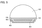
- FIG. 5 is an example of a cross-sectional view of the light-emitting device which is one embodiment of the present invention.
- a structure in which an organic EL element is used as a solid light-emitting element is described as an example.
- the organic EL element is fabricated over the high refractive index substrate 102.
- the organic EL element includes a first electrode 401, an EL layer 403, and a second electrode 405.
- a detailed method for fabricating the organic EL element is described in Embodiment 2.
- the high refractive index liquid layer 104 is formed, and sealing is performed with the high refractive index component 103 which is molded to be hemispherical.
- the light-emitting device of this embodiment can be fabricated.
- the solid light-emitting element (here, an organic light-emitting element) is fabricated over the high refractive index substrate 102 first; however, the solid light-emitting element may be fabricated after the high refractive index liquid layer 104 and the high refractive index component 103 are fixed to the high refractive index substrate 102. In this case, a step in which a material used for the high refractive index component 103 is formed to have an uneven structure such as a hemispherical shape may be performed either before or after the fabrication of the solid light-emitting element.
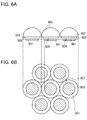
- FIGS. 6A and 6B Other structures of the light-emitting device which is one embodiment of the present invention are described with reference to FIGS. 6A and 6B .
- FIG. 6A is an example of a cross-sectional view of the light-emitting device
- FIG. 6B is an example of a plan view of the light-emitting device.
- the light-emitting device in FIGS. 6A and 6B include a plurality of solid light-emitting elements 601, a high refractive index substrate 602 having a plurality of depression portions each of which overlaps with each of the solid light-emitting elements 601, a high refractive index liquid layer 604 in the depression portion, and a plurality of high refractive index components 603 each of which overlaps with each of the solid light-emitting elements 601. That is, the light-emitting device illustrated in FIGS. 6A and 6B includes a plurality of elements each having a pair of the solid light-emitting element 601 and the hemispherical high refractive index component 603.
- the plurality of elements are arranged with a closest packed structure. Seven elements are illustrated in FIG. 6B , but the number of the elements is not limited thereto; the light-emitting device may include a plurality of elements.
- the high refractive index component 603 may also have a structure in which a plurality of hemispherical components are integrated to form one component (also referred to as an integrated component).
- An integrated component includes a plurality of hemispherical portions.
- the closest packed structure means a structure in which in a portion 607 where the plurality of hemispherical components are adjacent to each other, a space is not formed as much as possible but also includes a structure in which some spaces are formed owing to an error in design.
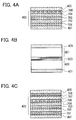
- FIGS. 4A to 4C a solid light-emitting element included in a light-emitting element which is one embodiment of the present invention is described with reference to FIGS. 4A to 4C .
- a light-emitting element illustrated in FIG. 4A includes the first electrode 401, the EL layer 403 over the first electrode 401, and the second electrode 405 over the EL layer 403.
- the first electrode 401 is formed. Since light from the EL layer 403 is extracted through the first electrode 401, the first electrode 401 is formed using a light-transmitting material.
- the first electrode 401 a metal material such as gold, platinum, nickel, tungsten, chromium, molybdenum, iron, cobalt, copper, palladium, or titanium can be used. Further, a nitride of the metal material (such as titanium nitride) or the like may be used. In the case of using the metal material (or the nitride thereof), the first electrode 401 may be thinned so as to be able to transmit light.
- a metal material such as gold, platinum, nickel, tungsten, chromium, molybdenum, iron, cobalt, copper, palladium, or titanium can be used.
- a nitride of the metal material such as titanium nitride
- the first electrode 401 may be thinned so as to be able to transmit light.
- the EL layer 403 is formed over the first electrode 401.
- the EL layer 403 includes the hole-injection layer 701, the hole-transport layer 702, the light-emitting layer 703, the electron-transport layer 704, and the electron-injection layer 705.
- the hole-injection layer 701 is a layer that contains a substance having a high hole-injection property.
- a substance having a high hole-injection property for example, a metal oxide such as molybdenum oxide, titanium oxide, vanadium oxide, rhenium oxide, ruthenium oxide, chromium oxide, zirconium oxide, hafnium oxide, tantalum oxide, silver oxide, tungsten oxide, or manganese oxide can be used.
- a phthalocyanine-based compound such as phthalocyanine (abbreviation: H 2 Pc), or copper(II) phthalocyanine (abbreviation: CuPc) can also be used.
- any of the following aromatic amine compounds which are low molecular organic compounds can be used: 4,4',4"-tris( N,N -diphenylamino)triphenylamine (abbreviation: TDATA), 4,4',4"-tris[ N -(3-methylphenyl)- N -phenylamino]triphenylamine (abbreviation: MTDATA), 4,4'-bis[ N -(4-diphenylaminophenyl)- N -phenylamino]biphenyl (abbreviation: DPAB), 4,4'-bis( N- ⁇ 4-[ N '-(3-methylphenyl)- N '-phenylamino]phenyl ⁇ - N phenylamino)biphenyl (abbreviation: DNTPD), 1,3,5-tris[ N -(4-diphenylaminophenyl)- N- phenylamino]benzene (abbreviation: T
- a high molecular compound to which acid is added such as poly(3,4-ethylenedioxythiophene)/poly(styrenesulfonic acid) (PEDOT/PSS) or polyaniline/poly(styrenesulfonic acid) (PAni/PSS), can be used.
- PEDOT/PSS poly(3,4-ethylenedioxythiophene)/poly(styrenesulfonic acid)
- PAni/PSS polyaniline/poly(styrenesulfonic acid)
- a composite material in which an acceptor substance is mixed with an organic compound having a high hole-transport property is preferably used for the hole-injection layer 701.
- a composite material in which an acceptor substance is added to a substance having a high hole-transport property hole injection from the first electrode 401 is facilitated, which leads to a reduction in the driving voltage of the light-emitting element.
- Such a composite material can be formed by co-evaporating a substance having a high hole-transport property and an acceptor substance.
- the hole-injection layer 701 is formed using the composite material, whereby hole injection from the first electrode 401 to the EL layer 403 is facilitated.
- any of various compounds such as aromatic amine compounds, carbazole derivatives, aromatic hydrocarbon, and high molecular compounds (e.g., oligomer, dendrimer, or polymer) can be used.
- the organic compound used for the composite material is preferably an organic compound having a high hole-transport property. Specifically, a substance having a hole mobility of 10 -6 cm 2 /Vs or higher is preferably used. However, a substance other than these substances may also be used as long as a hole-transport property thereof is higher than an electron-transport property thereof.
- the organic compounds which can be used for the composite material are specifically shown below.
- an aromatic hydrocarbon compound such as 2,3,6,7-tetramethyl-9,10-di(2-naphthyl)anthracene, 9,9'-bianthryl, 10,10'-diphenyl-9,9'-bianthryl, 10,10'-bis(2-phenylphenyl)-9,9'-bianthryl, 10,10'-bis[(2,3,4,5,6-pentaphenyl)phenyl]-9,9'-bianthryl, anthracene, tetracene, rubrene, perylene, 2,5,8,11-tetra( tert -butyl)perylene, pentacene, coronene, 4,4'-bis(2,2-diphenylvinyl)biphenyl (abbreviation: DPVBi), or 9,10-bis[4-(2,2-diphenylvinyl)phenyl]anthracene (abbreviation: DPVPA) can be used.
- DPVBi
- organic compounds such as 7,7,8,8-tetracyano-2,3,5,6-tetrafluoroquinodimethane (abbreviation: F 4 -TCNQ) and chloranil; and transition metal oxides can be given.
- oxides of metals belonging to Groups 4 to 8 in the periodic table can also be given.
- vanadium oxide, niobium oxide, tantalum oxide, chromium oxide, molybdenum oxide, tungsten oxide, manganese oxide, and rhenium oxide are preferable since their electron-accepting property is high.
- molybdenum oxide is especially preferable since it is stable in air and its hygroscopic property is low and is easily treated.
- the composite material may be formed using the above-described electron acceptor and the above-described high molecular compound such as PVK, PVTPA, PTPDMA, or Poly-TPD and used for the hole-injection layer 701.
- the hole-transport layer 702 is a layer that contains a substance having a high hole-transport property.
- a substance having a high hole-transport property any of the following aromatic amine compounds can be used, for example: NPB; TPD; BPAFLP; 4,4'-bis[ N- (9,9-dimethylfluoren-2-yl)- N -phenylamino]biphenyl (abbreviation: DFLDPBi); and 4,4'-bis[ N -(spiro-9,9'-bifluoren-2-yl)- N -phenylamino]biphenyl (abbreviation: BSPB).
- the substances mentioned here mainly have a hole mobility of 10 -6 cm 2 /Vs or higher.
- the layer that contains a substance having a high hole-transport property is not limited to a single layer, and two or more layers that contain the above-described substances may be stacked.
- a carbazole derivative such as CBP, CzPA, or PCzPA or an anthracene derivative such as t-BuDNA, DNA, or DPAnth may be used.
- a high molecular compound such as PVK, PVTPA, PTPDMA, or Poly-TPD can be used.
- the light-emitting layer 703 is a layer that contains an organic compound having a light-emitting property.
- an organic compound having a light-emitting property for example, a fluorescent compound which exhibits fluorescence or a phosphorescent compound which exhibits phosphorescence can be used.
- the fluorescent compounds that can be used for the light-emitting layer 703 are given below.
- Examples of the materials that emit blue light include N,N '-bis[4-(9 H- carbazol-9-yl)phenyl)- N , N '-diphenylstilbene-4,4'-diamine (abbreviation: YGA2S), 4-(9 H- carbazol-9-yl)-4'-(10-phenyl-9-anthryl)triphenylamine (abbreviation: YGAPA), 4-(10-phenyl-9-anthryl)-4'-(9-phenyl-9 H -carbazol-3-yl)triphenylamine (abbreviation: PCBAPA), and the like.
- examples of the materials that emit green light include N- (9,10-diphenyl-2-anthryl)- N ,9-diphenyl-9 H- carbazol-3-amine (abbreviation: 2PCAPA), N -[9,10-bis(1,1'-biphenyl-2-yl)-2-anthryl]- N ,9-diphenyl-9 H -carbazol-3-amine (abbreviation: 2PCABPhA), N- (9,10-diphenyl-2-anthryl)- N,N',N '-triphenyl-1,4-phenylenediamine (abbreviation: 2DPAPA), N -[9,10-bis(1,1'-biphenyl-2-yl)-2-anthryl)- N,N',N' -triphenyl-1,4-phenylenediamine (abbreviation: 2DPABPhA), N -[9,10-bis(1,1'-biphenyl-2
- examples of the materials that emit yellow light include rubrene, 5,12-bis(1,1'-biphenyl-4-yl)-6,11-diphenyltetracene (abbreviation: BPT), and the like.
- examples of the materials that emit red light include N,N,N',N '-tetrakis(4-methylphenyl)tetracene-5,11-diamine (abbreviation: p-mPhTD), 7,14-diphenyl- N,N,N',N '-tetrakis(4-methylphenyl)acenaphtho[1,2-a)fluoranthene-3,10-d iamine (abbreviation: p-mPhAFD), and the like.
- the phosphorescent compounds that can be used for the light-emitting layer 703 are given below.
- the materials that emit blue light include bis[2-(4',6'-difluorophenyl)pyridinato- N , C 2' ]iridium(III)tetrakis(1-pyrazolyl)borate (abbreviation: FIr6), bis[2-(4',6'-difluorophenyl)pyridinato- N , C 2 ' ]iridium(III)picolinate (abbreviation: FIrpic), bis ⁇ 2-[3',5'-bis(trifluoromethyl)phenyl)pyridinato- N , C 2' ⁇ iridium(III) picolinate (abbreviation: Ir(CF 3 ppy) 2 (pic)), bis[2-(4',6'-difluorophenyl)pyridinato- N , C 2' ]iridium(III
- Examples of the materials that emit green light include tris(2-phenylpyridinato- N , C 2' )iridium(III) (abbreviation: Ir(ppy) 3 ), bis(2-phenylpyridinato- N , C 2' )iridium(III)acetylacetonate (abbreviation: Ir(ppy) 2 (acac)), bis(1,2-diphenyl-1 H -benzimidazolato)iridium(III)acetylacetonate (abbreviation: Ir(pbi) 2 (acac)), bis(benzo[ h ]quinolinato)iridium(III)acetylacetonate (abbreviation: Ir(bzq) 2 (acac)), tris(benzo[ h ]quinolinato)iridium(III) (abbreviation: Ir(bzq) 3 ), and the like.
- Examples of the materials that emit yellow light include bis(2,4-diphenyl-1,3-oxazolato- N , C 2' )iridium(III)acetylacetonate (abbreviation: Ir(dpo) 2 (acac)), bis[2-(4'-(perfluorophenylphenyl)pyridinato]iridium(III)acetylacetonate (abbreviation: Ir(p-PF-ph) 2 (acac)), bis(2-phenylbenzothiazolato- N , C 2 ' )iridium(III)acetylacetonate (abbreviation: Ir(bt) 2 (acac)), (acetylacetonato)bis[2,3-bis(4-fluorophenyl)-5-methylpyrazinato]iridium(III) (abbreviation: Ir(Fdppr-Me) 2 (acac)), (acet
- Examples of the materials that emit orange light include tris(2-phenylquinolinato- N , C 2' )iridium(III) (abbreviation: Ir(pq) 3 ), bis(2-phenylquinolinato- N , C 2' )iridium(III)acetylacetonate (abbreviation: Ir(pq) 2 (acac)), (acetylacetonato)bis(3,5-dimethyl-2-phenylpyrazinato)iridium(III) (abbreviation: Ir(mppr-Me) 2 (acac)), (acetylacetonato)bis(5-isopropyl-3-methyl-2-phenylpyrazinato)iridium(III) (abbreviation: Ir(mppr-iPr) 2 (acac)), and the like.
- Ir(pq) 3 bis(2-phenylquinolinato- N , C 2' )iridium
- Examples of the materials that emit red light include organometallic complexes such as bis[2-(2'-benzo[4,5- ⁇ ]thienyl)pyridinato- N , C 3' )iridium(III)acetylacetonate (abbreviation: Ir(btp) 2 (acac)), bis(1-phenylisoquinolinato- N , C 2' )iridium(III)acetylacetonate (abbreviation: Ir(piq) 2 (acac), (acetylacetonato)bis[2,3-bis(4-fluorophenyl)quinoxalinato]iridium(III) (abbreviation: Ir(Fdpq) 2 (acac)), (acetylacetonato)bis(2,3,5-triphenylpyrazinato)iridium(III) (abbreviation: lr(tppr) 2 (acac)), (dipivalo
- any of the following rare earth metal complexes can be used as a phosphorescent compound: tris(acetylacetonato)(monophenanthroline)terbium(III) (abbreviation: Tb(acac) 3 (Phen)); tris(1,3-diphenyl-1,3-propanedionato)(monophenanthroline)europium(III) (abbreviation: Eu(DBM) 3 (Phen)); and tris[1-(2-thenoyl)-3,3,3-trifluoroacetonato](monophenanthroline)europium(III) (abbreviation: Eu(TTA) 3 (Phen)), because their light emission (generated by electronic transition between different multiplicities) is from a rare earth metal ion.
- the light-emitting layer 703 may have a structure in which the above-described light-emitting organic compound (a guest material) is dispersed in another substance (a host material).
- a host material various kinds of materials can be used, and it is preferable to use a substance which has a lowest unoccupied molecular orbital level (LUMO level) higher than the light-emitting substance and has a highest occupied molecular orbital level (HOMO level) lower than that of the light-emitting substance.
- LUMO level lowest unoccupied molecular orbital level
- HOMO level highest occupied molecular orbital level
- a metal complex such as tris(8-quinolinolato)aluminum(III) (abbreviation: Alq), tris(4-methyl-8-quinolinolato)aluminum(III) (abbreviation: Almq 3 ), bins(10-hydroxybenzo[ h ]quinolinato)beryllium(II) (abbreviation: BeBq 2 ), bis(2-methyl-8-quinolinolato)(4-phenylphenolato)aluminum(III) (abbreviation: BAlq), bis(8-quinolinolato)zinc(II) (abbreviation: Znq), bis[2-(2-benzoxazolyl)phenolato]zinc(II) (abbreviation: ZnPBO), or bis[2-(2-benzothiazolyl)phenolato]zinc(II) (abbreviation: ZnBTZ); a heterocyclic compound
- the host material plural kinds of materials can be used.
- a substance such as rubrene which suppresses crystallization may be further added.
- NPB, Alq, or the like may be further added in order to efficiently transfer energy to the guest material.
- crystallization of the light-emitting layer 703 can be suppressed. Further, concentration quenching due to high concentration of the guest material can be suppressed.
- a high molecular compound can be used for the light-emitting layer 703, a high molecular compound.
- the materials that emit blue light include poly(9,9-dioctylfluorene-2,7-diyl) (abbreviation: PFO), poly[(9,9-dioctylfluorene-2,7-diyl)- co -(2,5-dimethoxybenzene-1,4-diyl)] (abbreviation: PF-DMOP), poly ⁇ (9,9-dioctylfluorene-2,7-diyl)- co -[ N , N '-di-( p -butylphenyl)-1,4-diaminobenzene] ⁇ (abbreviation: TAB-PFH), and the like.
- examples of the materials that emit green light include poly( p -phenylenevinylene) (abbreviation: PPV), poly[(9,9-dihexylfluorene-2,7-diyl)- alt - co -(benzo[2,1,3]thiadiazole-4,7-diyl)] (abbreviation: PFBT), poly[(9,9-dioctyl-2,7-divinylenefluorenylene)- alt - co -(2-methoxy-5-(2-ethylhexyloxy)-1 ,4-phenylene)], and the like.
- PPV poly( p -phenylenevinylene)
- PFBT poly[(9,9-dihexylfluorene-2,7-diyl)- alt - co -(benzo[2,1,3]thiadiazole-4,7-diyl)]
- PFBT poly[(9,9
- examples of the materials that emit orange to red light include poly[2-methoxy-5-(2'-ethylhexoxy)-1,4-phenylenevinylene] (abbreviation: MEH-PPV), poly(3-butylthiophene-2,5-diyl) (abbreviation: R4-PAT), poly ⁇ [9,9-dihexyl-2,7-bis(1-cyanovinylene)fluorenylene]- alt - co -[2,5-bis( N , N' -diphenyl amino)-1,4-phenylene] ⁇ , poly ⁇ [2-methoxy-5-(2-ethylhexyloxy)-1,4-bis(1-cyanovinylenephenylene)]- alt - co -[2,5-bis( N , N' -diphenylamino)-1,4-phenylene] ⁇ (abbreviation: CN-PPV-DPD), and the like.
- the emission colors of first and second light-emitting layers are complementary in a light-emitting element having the two light-emitting layers, whereby the light-emitting element can be made to emit white light as a whole.
- the word "complementary" means color relationship in which an achromatic color is obtained when colors are mixed. That is, emission of white light can be obtained by mixture of light emitted from substances whose emission colors are complementary colors. This can be applied to a light-emitting element having three or more light-emitting layers.
- the electron-transport layer 704 is a layer that contains a substance having a high electron-transport property.
- a substance having a high electron-transport property any of the following substances can be used, for example: a metal complex having a quinoline skeleton or a benzoquinoline skeleton such as tris(8-quinolinolato)aluminum (abbreviation: Alq), tris(4-methyl-8-quinolinolato)aluminum (abbreviation: Almq 3 ), bis(10-hydroxybenzo[ h ]quinolinato)beryllium (abbreviation: BeBq 2 ), or bis(2-methyl-8-quinolinolato)(4-phenylphenolato)aluminum (abbreviation: BAlq).
- Alq tris(8-quinolinolato)aluminum
- Almq 3 tris(4-methyl-8-quinolinolato)aluminum
- BeBq 2 bis(
- a metal complex or the like including an oxazole-based or thiazole-based ligand such as bis[2-(2-hydroxyphenyl)benzoxazolato]zinc (abbreviation: Zn(BOX) 2 ) or bis[2-(2-hydroxyphenyl)benzothiazolato]zinc (abbreviation: Zn(BTZ) 2 ) can be used.
- 2-(4-biphenylyl)-5-(4- tert -butylphenyl)-1,3,4-oxadiazole (abbreviation: PBD), 1,3-bis[5-(p- tert -butylphenyl)-1,3,4-oxadiazol-2-yl]benzene (abbreviation: OXD-7), 3-(4-biphenylyl)-4-phenyl-5-(4- tert -butylphenyl)-1,2,4-triazole (abbreviation: TAZ), bathophenanthroline (abbreviation: BPhen), bathocuproine (abbreviation: BCP), or the like can also be used.
- the substances mentioned here mainly have an electron mobility of 10 -6 cm 2 /Vs or higher.
- the electron-transport layer is not limited to a single layer, and two or more layers that contains the above-described substances may be stacked.
- the electron-injection layer 705 is a layer that contains a substance having a high electron-injection property.
- an alkali metal, an alkaline-earth metal, or a compound thereof, such as lithium, cesium, calcium, lithium fluoride, cesium fluoride, calcium fluoride, or lithium oxide can be used.
- a rare earth metal compound such as erbium fluoride can also be used. Any of the substances contained in the electron-transport layer 704 which are given above can also be used.
- the hole-injection layer 701, the hole-transport layer 702, the light-emitting layer 703, the electron-transport layer 704, and the electron-injection layer 705 which are described above can each be formed by a method such as an evaporation method (e.g., a vacuum evaporation method), an ink-jet method, or a coating method.
- a method such as an evaporation method (e.g., a vacuum evaporation method), an ink-jet method, or a coating method.
- a plurality of EL layers may be stacked between the first electrode 401 and the second electrode 405 as illustrated in FIG. 4B .
- a charge generation layer 803 is preferably provided between a first EL layer 800 and a second EL layer 801 which are stacked.
- the charge generation layer 803 can be formed using the above-mentioned composite material.
- the charge generation layer 803 may have a stacked structure including a layer that contains the composite material and a layer that contains another material. In that case, as the layer that contains another material, a layer that contains an electron-donating substance and a substance having a high electron-transport property, a layer formed of a transparent conductive film, or the like can be used.
- a light-emitting element having such a structure problems such as energy transfer and quenching hardly occur, and a light-emitting element which has both high emission efficiency and a long lifetime can be easily obtained due to expansion in the choice of materials. Moreover, a light-emitting element which provides phosphorescence from one of the EL layers and fluorescence from the other of the EL layers can be readily obtained. Note that this structure can be combined with the above-described structures of the EL layer.
- a light-emitting element as a whole can provide light emission of a desired color. For example, by forming a light-emitting element having two EL layers such that the emission color of the first EL layer and the emission color of the second EL layer are complementary colors, the light-emitting element can emit white light as a whole. This can be applied to a light-emitting element having three or more EL layers.
- the EL layer 403 may include the hole-injection layer 701, the hole-transport layer 702, the light-emitting layer 703, the electron-transport layer 704, an electron-injection buffer layer 706, an electron-relay layer 707, and a composite material layer 708 which is in contact with the second electrode 405, between the first electrode 401 and the second electrode 405.
- the composite material layer 708 which is in contact with the second electrode 405, in which case damage caused to the EL layer 403 particularly when the second electrode 405 is formed by a sputtering method can be reduced.
- the composite material layer 708 can be formed using the above-described composite material in which an acceptor substance is mixed with an organic compound having a high hole-transport property.
- an injection barrier between the composite material layer 708 and the electron-transport layer 704 can be reduced; thus, electrons generated in the composite material layer 708 can be easily injected to the electron-transport layer 704.
- a substance having a high electron-injection property can be used for the electron-injection buffer layer 706: for example, an alkali metal, an alkaline earth metal, a rare earth metal, a compound of the above metal (e.g., an alkali metal compound (including an oxide such as lithium oxide, a halide, or carbonate such as lithium carbonate or cesium carbonate), an alkaline earth metal compound (e.g., an oxide, a halide, or carbonate), or a rare earth metal compound (e.g., an oxide, a halide, or carbonate).
- an alkali metal compound including an oxide such as lithium oxide, a halide, or carbonate such as lithium carbonate or cesium carbonate
- an alkaline earth metal compound e.g., an oxide, a halide, or carbonate
- a rare earth metal compound e.g., an oxide, a halide, or carbonate
- the donor substance is preferably added so that the mass ratio of the donor substance to the substance having a high electron-transport property is from 0.001:1 to 0.1:1.
- an organic compound such as tetrathianaphthacene (abbreviation: TTN), nickelocene, or decamethylnickelocene can be used as well as an alkali metal, an alkaline earth metal, a rare earth metal, a compound of the above metal (e.g., an alkali metal compound (including an oxide of lithium oxide or the like, a halide, and carbonate such as lithium carbonate or cesium carbonate), an alkaline earth metal compound (including an oxide, a halide, and carbonate), and a rare earth metal compound (including an oxide, a halide, and carbonate).
- TTN tetrathianaphthacene
- nickelocene nickelocene
- decamethylnickelocene can be used as well as an alkali metal, an alkaline earth metal, a rare earth metal, a compound of the above metal (e.g., an alkali metal compound (including an oxide of lithium oxide or the like,
- the electron-relay layer 707 is preferably formed between the electron-injection buffer layer 706 and the composite material layer 708.
- the electron-relay layer 707 is not necessarily provided; however, by providing the electron-relay layer 707 having a high electron-transport property, electrons can be rapidly transported to the electron-injection buffer layer 706.
- the structure in which the electron-relay layer 707 is sandwiched between the composite material layer 708 and the electron-injection buffer layer 706 is a structure in which the acceptor substance contained in the composite material layer 708 and the donor substance contained in the electron-injection buffer layer 706 are less likely to interact with each other, and thus their functions hardly interfere with each other. Therefore, an increase in the driving voltage can be suppressed.
- the electron-relay layer 707 contains a substance having a high electron-transport property and is formed so that the LUMO level of the substance having a high electron-transport property is located between the LUMO level of the acceptor substance contained in the composite material layer 708 and the LUMO level of the substance having a high electron-transport property contained in the electron-transport layer 704.
- the donor level of the donor substance is controlled so as to be located between the LUMO level of the acceptor substance contained in the composite material layer 708 and the LUMO level of the substance having a high electron-transport property contained in the electron-transport layer 704.
- the LUMO level of the substance having a high electron-transport property contained in the electron-relay layer 707 is preferably greater than or equal to -5.0 eV, more preferably greater than or equal to -5.0 eV and less than or equal to -3.0 eV.
- a phthalocyanine-based material or a metal complex having a metal-oxygen bond and an aromatic ligand is preferably used.
- phthalocyanine-based material contained in the electron-relay layer 707 for example, any of CuPc, phthalocyanine tin(II) complex (SnPc), phthalocyanine zinc complex (ZnPc), cobalt(II) phthalocyanine, ⁇ -form (CoPc), phthalocyanine iron (FePc), and vanadyl 2,9,16,23-tetraphenoxy-29 H ,31 H -phthalocyanine (PhO-VOPc), is preferably used.
- any of CuPc, phthalocyanine tin(II) complex (SnPc), phthalocyanine zinc complex (ZnPc), cobalt(II) phthalocyanine, ⁇ -form (CoPc), phthalocyanine iron (FePc), and vanadyl 2,9,16,23-tetraphenoxy-29 H ,31 H -phthalocyanine (PhO-VOPc) is
- a metal complex having a metal-oxygen double bond is preferably used as the metal complex having a metal-oxygen bond and an aromatic ligand, which is contained in the electron-relay layer 707.
- the metal-oxygen double bond has acceptor properties (properties of easily accepting electrons); thus, electrons can be transferred (donated and accepted) more easily. Further, the metal complex which has a metal-oxygen double bond is considered stable. Thus, the use of the metal complex having the metal-oxygen double bond enables the light-emitting element to drive at low voltage more stably.
- a phthalocyanine-based material As a metal complex having a metal-oxygen bond and an aromatic ligand, a phthalocyanine-based material is preferable. Specifically, any of vanadyl phthalocyanine (VOPc), a phthalocyanine tin(IV) oxide complex (SnOPc), and a phthalocyanine titanium oxide complex (TiOPc) is preferable because a metal-oxygen double bond is likely to act on another molecular in terms of a molecular structure and an acceptor property is high.
- VOPc vanadyl phthalocyanine
- SnOPc phthalocyanine tin(IV) oxide complex
- TiOPc phthalocyanine titanium oxide complex
- a phthalocyanine-based material having a phenoxy group is preferable.
- a phthalocyanine derivative having a phenoxy group such as PhO-VOPc, is preferable.
- the phthalocyanine derivative having a phenoxy group is soluble in a solvent; thus, the phthalocyanine derivative has an advantage of being easily handled during formation of a light-emitting element and an advantage of facilitating maintenance of an apparatus used for film formation.
- the electron-relay layer 707 may further contain a donor substance.
- a donor substance an organic compound such as tetrathianaphthacene (abbreviation: TTN), nickelocene, or decamethylnickelocene can be used as well as an alkali metal, an alkaline earth metal, a rare earth metal, and a compound of the above metal (e.g., an alkali metal compound (including an oxide such as lithium oxide, a halide, and a carbonate such as lithium carbonate or cesium carbonate), an alkaline earth metal compound (including an oxide, a halide, and carbonate), and a rare earth metal compound (including an oxide, a halide, and carbonate)).
- TTN tetrathianaphthacene
- nickelocene nickelocene
- decamethylnickelocene can be used as well as an alkali metal, an alkaline earth metal, a rare earth metal, and a compound of the above
- a substance having a LUMO level greater than the acceptor level of the acceptor substance contained in the composite material layer 708 can be used.
- a LUMO level is greater than or equal to -5.0 eV, preferably greater than or equal to -5.0 eV and less than or equal to -3.0 eV.
- a perylene derivative and a nitrogen-containing condensed aromatic compound can be given. Note that a nitrogen-containing condensed aromatic compound is preferably used for the electron-relay layer 707 because of its stability.
- perylene derivative the following can be given: 3,4,9,10-perylenetetracarboxylicdianhydride (abbreviation: PTCDA), 3,4,9,10-perylenetetracarboxylic-bis-benzimidazole (abbreviation: PTCBI), N,N'-dioctyl-3,4,9,10-perylenetetracarboxylic diimide (abbreviation: PTCDI-C8H), N,N'-dihexyl-3,4,9,10-perylenetetracarboxylic diimide (Hex PTC), and the like.
- PTCDA 3,4,9,10-perylenetetracarboxylicdianhydride
- PTCBI 3,4,9,10-perylenetetracarboxylic-bis-benzimidazole
- PTCDI-C8H N,N'-dihexyl-3,4,9,10-perylenetetracarboxylic diimi
- the nitrogen-containing condensed aromatic compound As specific examples of the nitrogen-containing condensed aromatic compound, the following can be given: pirazino[2,3- f ][1,10]phenanthroline-2,3-dicarbonitrile (PPDN), 2,3,6,7,10,11-hexacyano-1,4,5,8,9,12-hexaazatriphenylene (HAT(CN) 6 ), 2,3-diphenylpyrido[2,3- b ]pyrazine (2PYPR), 2,3-bis(4-fluorophenyl)pyrido[2,3- b ]pyrazine (F2PYPR), and the like.
- PPDN 2,3,6,7,10,11-hexacyano-1,4,5,8,9,12-hexaazatriphenylene
- HAT(CN) 6 2,3-diphenylpyrido[2,3- b ]pyrazine
- 2PYPR 2,3-bis(4-fluor
- the electron-relay layer 707 may be formed by a method such as co-evaporation of the substance having a high electron-transport property and the donor substance.
- the hole-injection layer 701, the hole-transport layer 702, the light-emitting layer 703, and the electron-transport layer 704 may each be formed using any of the above-described materials.
- a second electrode 405 is formed over the EL layer 403.
- the second electrode 405 is provided on the side opposite to the side from which light is extracted and is formed using a reflective material.
- a metal material such as aluminum, gold, platinum, silver, nickel, tungsten, chromium, molybdenum, iron, cobalt, copper, or palladium can be used.
- an alloy containing aluminum such as an alloy of aluminum and titanium, an alloy of aluminum and nickel, or an alloy of aluminum and neodymium, or an alloy containing silver such as an alloy of silver and copper can be used.
- the alloy of silver and copper is preferable because it has high heat resistance.
- a metal film or a metal oxide film in contact with the aluminum alloy film, oxidation of the aluminum alloy film can be suppressed.
- a material for the metal film and the metal oxide film include titanium, titanium oxide, and the like. The above materials are preferable because they are present in large amounts in the Earth's crust and inexpensive to achieve a reduction in the cost of manufacturing a light-emitting element.
- the solid light-emitting element of this embodiment can be fabricated.
- FIG. 7A illustrates a lighting device (desk lamp), which includes a lighting portion 7501, a shade 7502, an adjustable arm 7503, a support 7504, a base 7505, and a power switch 7506.
- the lighting device is manufactured by using a light-emitting device, which is manufactured according to one embodiment of the present invention, for the lighting portion 7501.
- the term "lighting device” also encompasses ceiling lights (ceiling-fixed lighting devices), wall lights (wall-hanging lighting devices), and the like, as well as the desk lamp illustrated in FIG. 7A .
- the lighting device which has high power efficiency and light-extraction efficiency and emits light uniformly in a plane can be provided.
- FIG. 7B shows examples in each of which a light-emitting device to which one embodiment of the present invention is applied is used for an interior lighting device.
- the light-emitting device which is one embodiment of the present invention is advantageous in increasing the area, and thus can be used as a lighting device having a large area as illustrated by a ceiling light 3001.
- the light-emitting device can be used for a wall-hanging lighting device 3002. Note that by using the light-emitting device to which one embodiment of the present invention is applied, a lighting device which has high power efficiency and high light-extraction efficiency and emits light uniformly in a plane can be provided.
- a desk lamp 3000 illustrated in FIG. 7A may be used together in a room provided with the interior lighting device.
- a light-emitting element was fabricated over one surface of a high refractive index substrate 1100.
- a glass substrate having a refractive index of 1.806 (S-LAH53 produced by Ohara Inc.) was used.
- indium tin oxide containing silicon oxide (ITSO) was deposited by a sputtering method, whereby a first electrode 1101 functioning as an anode was formed.
- the thickness thereof was 110 nm and the electrode area was 2 mm x 2 mm.
- UV ozone treatment was performed for 370 seconds.
- the substrate 1100 was transferred into a vacuum evaporation apparatus where the pressure had been reduced to approximately 10 -4 Pa, and subjected to vacuum baking at 150 °C for 1 hour in a heating chamber of the vacuum evaporation apparatus, and then the substrate 1100 was cooled down for about 30 minutes.
- the substrate 1100 on which the first electrode 1101 was formed was fixed to a substrate holder in a vacuum evaporation apparatus such that a surface of the substrate 1100 on which the first electrode 1101 was formed faced downward.
- the pressure in the vacuum evaporation apparatus was reduced to about 10 -4 Pa.
- 9-phenyl-3-[4-(10-phenyl-9-anthryl)phenyl]-9 H -carbazole (abbreviation: PCzPA) and molybdenum(VI) oxide were co-evaporated, whereby a first hole-injection layer 1111a was formed.
- the co-evaporation method means an evaporation method in which evaporation is carried out from a plurality of evaporation sources at the same time in one treatment chamber.
- PCzPA was deposited to a thickness of 30 nm, whereby a first hole-transport layer 1112a was formed.
- first hole-transport layer 1112a 9-[4-( N -carbazolyl)]phenyl-1-10-phenylanthracene (abbreviation: CzPA) and N,N' -bis[4-(9-phenyl-9 H- fluoren-9-yl)phenyl]- N,N '-diphenylpyrene-1,6-diamine (abbreviation: 1,6FLPAPrn) were co-evaporated, whereby a first light-emitting layer 1113a was formed.
- CzPA was deposited to a thickness of 5 nm and bathophenanthroline (abbreviation: BPhen) was deposited to a thickness of 15 nm, whereby a first electron-transport layer 1114a was formed.
- BPhen bathophenanthroline
- first electron-transport layer 1114a Li was evaporated to a thickness of 0.1 nm, whereby a first electron-injection layer 1115a was formed.
- first electron-injection layer 1115a copper phthalocyanine (abbreviation: CuPc) was evaporated to a thickness of 2 nm, whereby a first intermediate layer 1116a was formed.
- CuPc copper phthalocyanine
- PCzPA and molybdenum(VI) oxide were co-evaporated, whereby a second hole-injection layer 1111b was formed.
- the second hole-injection layer 1111b in this example functions as the charge generation layer described in the above embodiment.
- BPAFLP 4-phenyl-4'-(9-phenylfluoren-9-yl)triphenylamine
- 2-[3-(dibenzothiophen-4-yl)phenyl]dibenzo[ f,h ]quinoxaline (abbreviation: 2mDBTPDBq-II), 4-phenyl-4'-(9-phenyl-9 H- carbazol-3-yl)triphenylamine (abbreviation: PCBA1BP), and (acetylacetonato)bis(3,5-dimethyl-2-phenylpyrazinato)iridium(III) (abbreviation: Ir(mppr-Me) 2 (acac)) were co-evaporated, whereby a first layer of a second light-emitting layer 1113b was formed.
- 2mDBTPDBq-II and Ir(mppr-Me) 2 (acac) were co-evaporated, whereby a second layer was formed.
- 2mDBTPDBq-II was deposited to a thickness of 25 nm and Bphen was deposited to a thickness of 15 nm, whereby a second electron-transport layer 1114b was formed.
- Li was evaporated to a thickness of 0.1 nm, whereby a second electron-injection layer 1115b was formed.
- PCzPA and molybdenum(VI) oxide were co-evaporated, whereby a third hole-injection layer 1111 c was formed.
- the third hole-injection layer 1111c in this example functions as the charge generation layer described in the above embodiment.
- lithium fluoride (LiF) was evaporated to a thickness of 0.1 nm, whereby a third electron-injection layer 1115c was formed.
- the light-emitting element of this example was fabricated. Light emitted from the light-emitting element can be extracted to air through the first electrode 1101 and the high refractive index substrate 1100.
- the light-emitting element was sealed in a glove box under a nitrogen atmosphere so as not to be subjected to air. After that, at a position that is on a side of the substrate 1100 on which the light-emitting element was not formed, and that overlaps with a light-emitting region of the light-emitting element, a high refractive index component 1200 having a light-transmitting property was provided to form the light-emitting device.
- the high refractive index component 1200 was formed using a glass substrate having a refractive index of 2.003 (S-LAH79 produced by Edmund Optics Inc.) and has a hemispherical shape with a diameter of 1 cm.
- a cross-section of the hemisphere is connected to the high refractive index substrate 1100 via a catalytic liquid (a refractive index liquid) that contains sulfur and methylene iodide and has a refractive index of 1.78 (produced by Shimazu Device Corporation) (see a high refractive index liquid layer 1201 in FIG. 9 ).
- a catalytic liquid a refractive index liquid
- 1.78 produced by Shimazu Device Corporation
- current density vs. power efficiency characteristics of the light-emitting device shown in FIG. 8 indicate that by supplying current with a current density of 0.93 mA/cm 2 , the light-emitting device can obtain a power efficiency of 101 Im/W.
- the vertical axis represents power efficiency (lm/W)
- the horizontal axis represents current density (mA/cm 2 ).
- the current density of the solid light-emitting element controlled emission intensity of the solid light-emitting element, but did not affect spatial distribution of light emitted from the solid light-emitting element.
- the power efficiency (lm/W) is in proportion to the value obtained by dividing the current efficiency (cd/A) by the driving voltage (V). Accordingly, when the value obtained by dividing the current efficiency (cd/A) by the driving voltage (V) is multiplied by a proportionality constant, the current density (mA/cm 2 ) vs. power efficiency (lm/W) characteristics can be obtained.
- the proportionality constant can be obtained in the following manner.
- the first step the current density and the luminance of the solid light-emitting element at a specific driving voltage E 1 (V) were measured, the current efficiency ⁇ 1 ; (cd/A) was calculated, and the value ⁇ 1 /E 1 ) was obtained by dividing the current efficiency ⁇ 1 ; (cd/A) by the driving voltage E 1 (V).
- a hemispherical structural body was provided over the high refractive index substrate via a buffer solution at a position that overlaps with the light-emitting region of the same solid light-emitting element, whereby the light-emitting device was formed.
- the driving voltage E 1 (V) was applied to the light-emitting device, and power efficiency P 1 (lm/W) was measured with the use of the integrating sphere.
- P 1 was divided by ( ⁇ 1/ E 1 ), whereby the proportionality constant C was obtained.
- NMR nuclear magnetic resonance
Landscapes
- Chemical & Material Sciences (AREA)
- Physics & Mathematics (AREA)
- Engineering & Computer Science (AREA)
- Materials Engineering (AREA)
- Spectroscopy & Molecular Physics (AREA)
- Optics & Photonics (AREA)
- Crystallography & Structural Chemistry (AREA)
- Inorganic Chemistry (AREA)
- Electroluminescent Light Sources (AREA)
Applications Claiming Priority (1)
| Application Number | Priority Date | Filing Date | Title |
|---|---|---|---|
| JP2010206386 | 2010-09-15 |
Publications (2)
| Publication Number | Publication Date |
|---|---|
| EP2432039A1 EP2432039A1 (en) | 2012-03-21 |
| EP2432039B1 true EP2432039B1 (en) | 2016-12-07 |
Family
ID=44582691
Family Applications (1)
| Application Number | Title | Priority Date | Filing Date |
|---|---|---|---|
| EP11181085.9A Not-in-force EP2432039B1 (en) | 2010-09-15 | 2011-09-13 | Light-emitting device and lighting device |
Country Status (4)
| Country | Link |
|---|---|
| US (1) | US8624284B2 (ko) |
| EP (1) | EP2432039B1 (ko) |
| JP (1) | JP5840428B2 (ko) |
| KR (1) | KR101810589B1 (ko) |
Families Citing this family (4)
| Publication number | Priority date | Publication date | Assignee | Title |
|---|---|---|---|---|
| TWI540939B (zh) | 2010-09-14 | 2016-07-01 | 半導體能源研究所股份有限公司 | 固態發光元件,發光裝置和照明裝置 |
| WO2012053571A1 (en) | 2010-10-22 | 2012-04-26 | Semiconductor Energy Laboratory Co., Ltd. | Light-emitting element, light-emitting device, and lighting device |
| US8727586B2 (en) | 2010-11-05 | 2014-05-20 | Semiconductor Energy Laboratory Co., Ltd. | Lighting device having magnetic member and magnet |
| JP2016082239A (ja) * | 2014-10-16 | 2016-05-16 | 株式会社半導体エネルギー研究所 | 発光素子、発光装置、電子機器及び照明装置 |
Citations (2)
| Publication number | Priority date | Publication date | Assignee | Title |
|---|---|---|---|---|
| US20080087907A1 (en) * | 2006-10-11 | 2008-04-17 | Samsung Electro-Mechanics Co. Ltd | Light emitting diode package |
| WO2010026390A1 (en) * | 2008-09-04 | 2010-03-11 | Microsharp Corporation Limited | Light emitting device with improved light extraction |
Family Cites Families (18)
| Publication number | Priority date | Publication date | Assignee | Title |
|---|---|---|---|---|
| EP0781075B1 (en) | 1994-09-08 | 2001-12-05 | Idemitsu Kosan Company Limited | Method for sealing organic el element and organic el element |
| JP2000182769A (ja) | 1998-12-11 | 2000-06-30 | Kawaguchiko Seimitsu Co Ltd | エレクトロルミネッセンス及びそれを用いた表示機器 |
| US7112115B1 (en) | 1999-11-09 | 2006-09-26 | Semiconductor Energy Laboratory Co., Ltd. | Light emitting device and method of manufacturing the same |
| AU2002352967A1 (en) * | 2001-11-29 | 2003-06-10 | The Trustees Of Princeton University | Increased emission efficiency in organic light-emitting devices on high-index substrates |
| JP4027914B2 (ja) | 2004-05-21 | 2007-12-26 | 株式会社半導体エネルギー研究所 | 照明装置及びそれを用いた機器 |
| JP4770450B2 (ja) | 2005-12-21 | 2011-09-14 | パナソニック電工株式会社 | 有機el照明装置 |
| JP2008066027A (ja) | 2006-09-05 | 2008-03-21 | Fuji Electric Holdings Co Ltd | 凹凸表面を有する基板およびそれを用いた有機el素子 |
| JP5200361B2 (ja) | 2006-10-16 | 2013-06-05 | 凸版印刷株式会社 | 光学用部品の製造方法 |
| WO2008069162A1 (en) | 2006-12-05 | 2008-06-12 | Semiconductor Energy Laboratory Co., Ltd. | Anti-reflection film and display device |
| WO2008069223A1 (en) | 2006-12-05 | 2008-06-12 | Semiconductor Energy Laboratory Co., Ltd. | Anti-reflection film and display device |
| WO2008069219A1 (en) | 2006-12-05 | 2008-06-12 | Semiconductor Energy Laboratory Co., Ltd. | Antireflective film and display device |
| WO2008069221A1 (en) | 2006-12-05 | 2008-06-12 | Semiconductor Energy Laboratory Co., Ltd. | Plasma display panel and field emission display |
| JP2009110930A (ja) * | 2007-08-21 | 2009-05-21 | Fujifilm Corp | 散乱部材、及びこれを用いた有機エレクトロルミネッセンス表示装置 |
| JP5665160B2 (ja) | 2008-03-26 | 2015-02-04 | パナソニックIpマネジメント株式会社 | 発光装置および照明器具 |
| JP5038991B2 (ja) * | 2008-08-07 | 2012-10-03 | パナソニック株式会社 | 有機エレクトロルミネッセンス素子の設計方法 |
| GB2464111B (en) | 2008-10-02 | 2011-06-15 | Cambridge Display Tech Ltd | Organic electroluminescent device |
| JP2010118259A (ja) * | 2008-11-13 | 2010-05-27 | Kuraray Co Ltd | 面光源素子およびその製造方法 |
| JP2010206386A (ja) | 2009-03-02 | 2010-09-16 | Toshiba Corp | 映像信号処理装置及びその制御方法 |
-
2011
- 2011-09-09 KR KR1020110091904A patent/KR101810589B1/ko active IP Right Grant
- 2011-09-12 JP JP2011198088A patent/JP5840428B2/ja not_active Expired - Fee Related
- 2011-09-13 EP EP11181085.9A patent/EP2432039B1/en not_active Not-in-force
- 2011-09-14 US US13/232,671 patent/US8624284B2/en active Active
Patent Citations (2)
| Publication number | Priority date | Publication date | Assignee | Title |
|---|---|---|---|---|
| US20080087907A1 (en) * | 2006-10-11 | 2008-04-17 | Samsung Electro-Mechanics Co. Ltd | Light emitting diode package |
| WO2010026390A1 (en) * | 2008-09-04 | 2010-03-11 | Microsharp Corporation Limited | Light emitting device with improved light extraction |
Also Published As
| Publication number | Publication date |
|---|---|
| JP5840428B2 (ja) | 2016-01-06 |
| JP2012084517A (ja) | 2012-04-26 |
| KR101810589B1 (ko) | 2017-12-20 |
| US20120061708A1 (en) | 2012-03-15 |
| EP2432039A1 (en) | 2012-03-21 |
| US8624284B2 (en) | 2014-01-07 |
| KR20120028827A (ko) | 2012-03-23 |
Similar Documents
| Publication | Publication Date | Title |
|---|---|---|
| JP6480507B2 (ja) | 固体発光素子 | |
| JP6637579B2 (ja) | 発光装置 | |
| JP6412548B2 (ja) | 発光装置 | |
| JP2016189484A (ja) | 発光装置 | |
| US9121568B2 (en) | Lighting device | |
| US8669702B2 (en) | Lighting device | |
| JP6250019B2 (ja) | 発光装置 | |
| JP6093423B2 (ja) | 発光装置、照明装置および発光装置の作製方法 | |
| EP2432039B1 (en) | Light-emitting device and lighting device |
Legal Events
| Date | Code | Title | Description |
|---|---|---|---|
| PUAI | Public reference made under article 153(3) epc to a published international application that has entered the european phase |
Free format text: ORIGINAL CODE: 0009012 |
|
| AK | Designated contracting states |
Kind code of ref document: A1 Designated state(s): AL AT BE BG CH CY CZ DE DK EE ES FI FR GB GR HR HU IE IS IT LI LT LU LV MC MK MT NL NO PL PT RO RS SE SI SK SM TR |
|
| AX | Request for extension of the european patent |
Extension state: BA ME |
|
| 17P | Request for examination filed |
Effective date: 20120904 |
|
| 17Q | First examination report despatched |
Effective date: 20140317 |
|
| GRAP | Despatch of communication of intention to grant a patent |
Free format text: ORIGINAL CODE: EPIDOSNIGR1 |
|
| INTG | Intention to grant announced |
Effective date: 20160808 |
|
| GRAS | Grant fee paid |
Free format text: ORIGINAL CODE: EPIDOSNIGR3 |
|
| GRAA | (expected) grant |
Free format text: ORIGINAL CODE: 0009210 |
|
| AK | Designated contracting states |
Kind code of ref document: B1 Designated state(s): AL AT BE BG CH CY CZ DE DK EE ES FI FR GB GR HR HU IE IS IT LI LT LU LV MC MK MT NL NO PL PT RO RS SE SI SK SM TR |
|
| REG | Reference to a national code |
Ref country code: GB Ref legal event code: FG4D |
|
| REG | Reference to a national code |
Ref country code: CH Ref legal event code: EP Ref country code: AT Ref legal event code: REF Ref document number: 852414 Country of ref document: AT Kind code of ref document: T Effective date: 20161215 |
|
| REG | Reference to a national code |
Ref country code: IE Ref legal event code: FG4D |
|
| REG | Reference to a national code |
Ref country code: DE Ref legal event code: R096 Ref document number: 602011033075 Country of ref document: DE |
|
| PG25 | Lapsed in a contracting state [announced via postgrant information from national office to epo] |
Ref country code: LV Free format text: LAPSE BECAUSE OF FAILURE TO SUBMIT A TRANSLATION OF THE DESCRIPTION OR TO PAY THE FEE WITHIN THE PRESCRIBED TIME-LIMIT Effective date: 20161207 |
|
| REG | Reference to a national code |
Ref country code: LT Ref legal event code: MG4D |
|
| REG | Reference to a national code |
Ref country code: NL Ref legal event code: MP Effective date: 20161207 |
|
| PG25 | Lapsed in a contracting state [announced via postgrant information from national office to epo] |
Ref country code: GR Free format text: LAPSE BECAUSE OF FAILURE TO SUBMIT A TRANSLATION OF THE DESCRIPTION OR TO PAY THE FEE WITHIN THE PRESCRIBED TIME-LIMIT Effective date: 20170308 Ref country code: SE Free format text: LAPSE BECAUSE OF FAILURE TO SUBMIT A TRANSLATION OF THE DESCRIPTION OR TO PAY THE FEE WITHIN THE PRESCRIBED TIME-LIMIT Effective date: 20161207 Ref country code: NO Free format text: LAPSE BECAUSE OF FAILURE TO SUBMIT A TRANSLATION OF THE DESCRIPTION OR TO PAY THE FEE WITHIN THE PRESCRIBED TIME-LIMIT Effective date: 20170307 Ref country code: LT Free format text: LAPSE BECAUSE OF FAILURE TO SUBMIT A TRANSLATION OF THE DESCRIPTION OR TO PAY THE FEE WITHIN THE PRESCRIBED TIME-LIMIT Effective date: 20161207 |
|
| REG | Reference to a national code |
Ref country code: AT Ref legal event code: MK05 Ref document number: 852414 Country of ref document: AT Kind code of ref document: T Effective date: 20161207 |
|
| PG25 | Lapsed in a contracting state [announced via postgrant information from national office to epo] |
Ref country code: ES Free format text: LAPSE BECAUSE OF FAILURE TO SUBMIT A TRANSLATION OF THE DESCRIPTION OR TO PAY THE FEE WITHIN THE PRESCRIBED TIME-LIMIT Effective date: 20161207 Ref country code: FI Free format text: LAPSE BECAUSE OF FAILURE TO SUBMIT A TRANSLATION OF THE DESCRIPTION OR TO PAY THE FEE WITHIN THE PRESCRIBED TIME-LIMIT Effective date: 20161207 Ref country code: HR Free format text: LAPSE BECAUSE OF FAILURE TO SUBMIT A TRANSLATION OF THE DESCRIPTION OR TO PAY THE FEE WITHIN THE PRESCRIBED TIME-LIMIT Effective date: 20161207 Ref country code: RS Free format text: LAPSE BECAUSE OF FAILURE TO SUBMIT A TRANSLATION OF THE DESCRIPTION OR TO PAY THE FEE WITHIN THE PRESCRIBED TIME-LIMIT Effective date: 20161207 |
|
| PG25 | Lapsed in a contracting state [announced via postgrant information from national office to epo] |
Ref country code: NL Free format text: LAPSE BECAUSE OF FAILURE TO SUBMIT A TRANSLATION OF THE DESCRIPTION OR TO PAY THE FEE WITHIN THE PRESCRIBED TIME-LIMIT Effective date: 20161207 |
|
| PG25 | Lapsed in a contracting state [announced via postgrant information from national office to epo] |
Ref country code: SK Free format text: LAPSE BECAUSE OF FAILURE TO SUBMIT A TRANSLATION OF THE DESCRIPTION OR TO PAY THE FEE WITHIN THE PRESCRIBED TIME-LIMIT Effective date: 20161207 Ref country code: EE Free format text: LAPSE BECAUSE OF FAILURE TO SUBMIT A TRANSLATION OF THE DESCRIPTION OR TO PAY THE FEE WITHIN THE PRESCRIBED TIME-LIMIT Effective date: 20161207 Ref country code: RO Free format text: LAPSE BECAUSE OF FAILURE TO SUBMIT A TRANSLATION OF THE DESCRIPTION OR TO PAY THE FEE WITHIN THE PRESCRIBED TIME-LIMIT Effective date: 20161207 Ref country code: CZ Free format text: LAPSE BECAUSE OF FAILURE TO SUBMIT A TRANSLATION OF THE DESCRIPTION OR TO PAY THE FEE WITHIN THE PRESCRIBED TIME-LIMIT Effective date: 20161207 Ref country code: IS Free format text: LAPSE BECAUSE OF FAILURE TO SUBMIT A TRANSLATION OF THE DESCRIPTION OR TO PAY THE FEE WITHIN THE PRESCRIBED TIME-LIMIT Effective date: 20170407 |
|
| PG25 | Lapsed in a contracting state [announced via postgrant information from national office to epo] |
Ref country code: BE Free format text: LAPSE BECAUSE OF FAILURE TO SUBMIT A TRANSLATION OF THE DESCRIPTION OR TO PAY THE FEE WITHIN THE PRESCRIBED TIME-LIMIT Effective date: 20161207 Ref country code: SM Free format text: LAPSE BECAUSE OF FAILURE TO SUBMIT A TRANSLATION OF THE DESCRIPTION OR TO PAY THE FEE WITHIN THE PRESCRIBED TIME-LIMIT Effective date: 20161207 Ref country code: PT Free format text: LAPSE BECAUSE OF FAILURE TO SUBMIT A TRANSLATION OF THE DESCRIPTION OR TO PAY THE FEE WITHIN THE PRESCRIBED TIME-LIMIT Effective date: 20170407 Ref country code: BG Free format text: LAPSE BECAUSE OF FAILURE TO SUBMIT A TRANSLATION OF THE DESCRIPTION OR TO PAY THE FEE WITHIN THE PRESCRIBED TIME-LIMIT Effective date: 20170307 Ref country code: IT Free format text: LAPSE BECAUSE OF FAILURE TO SUBMIT A TRANSLATION OF THE DESCRIPTION OR TO PAY THE FEE WITHIN THE PRESCRIBED TIME-LIMIT Effective date: 20161207 Ref country code: AT Free format text: LAPSE BECAUSE OF FAILURE TO SUBMIT A TRANSLATION OF THE DESCRIPTION OR TO PAY THE FEE WITHIN THE PRESCRIBED TIME-LIMIT Effective date: 20161207 Ref country code: PL Free format text: LAPSE BECAUSE OF FAILURE TO SUBMIT A TRANSLATION OF THE DESCRIPTION OR TO PAY THE FEE WITHIN THE PRESCRIBED TIME-LIMIT Effective date: 20161207 |
|
| REG | Reference to a national code |
Ref country code: DE Ref legal event code: R097 Ref document number: 602011033075 Country of ref document: DE |
|
| PLBE | No opposition filed within time limit |
Free format text: ORIGINAL CODE: 0009261 |
|
| STAA | Information on the status of an ep patent application or granted ep patent |
Free format text: STATUS: NO OPPOSITION FILED WITHIN TIME LIMIT |
|
| 26N | No opposition filed |
Effective date: 20170908 |
|
| PG25 | Lapsed in a contracting state [announced via postgrant information from national office to epo] |
Ref country code: DK Free format text: LAPSE BECAUSE OF FAILURE TO SUBMIT A TRANSLATION OF THE DESCRIPTION OR TO PAY THE FEE WITHIN THE PRESCRIBED TIME-LIMIT Effective date: 20161207 Ref country code: SI Free format text: LAPSE BECAUSE OF FAILURE TO SUBMIT A TRANSLATION OF THE DESCRIPTION OR TO PAY THE FEE WITHIN THE PRESCRIBED TIME-LIMIT Effective date: 20161207 |
|
| REG | Reference to a national code |
Ref country code: CH Ref legal event code: PL |
|
| GBPC | Gb: european patent ceased through non-payment of renewal fee |
Effective date: 20170913 |
|
| PG25 | Lapsed in a contracting state [announced via postgrant information from national office to epo] |
Ref country code: MC Free format text: LAPSE BECAUSE OF FAILURE TO SUBMIT A TRANSLATION OF THE DESCRIPTION OR TO PAY THE FEE WITHIN THE PRESCRIBED TIME-LIMIT Effective date: 20161207 |
|
| REG | Reference to a national code |
Ref country code: IE Ref legal event code: MM4A |
|
| PG25 | Lapsed in a contracting state [announced via postgrant information from national office to epo] |
Ref country code: LU Free format text: LAPSE BECAUSE OF NON-PAYMENT OF DUE FEES Effective date: 20170913 |
|
| REG | Reference to a national code |
Ref country code: FR Ref legal event code: ST Effective date: 20180531 |
|
| PG25 | Lapsed in a contracting state [announced via postgrant information from national office to epo] |
Ref country code: GB Free format text: LAPSE BECAUSE OF NON-PAYMENT OF DUE FEES Effective date: 20170913 Ref country code: CH Free format text: LAPSE BECAUSE OF NON-PAYMENT OF DUE FEES Effective date: 20170930 Ref country code: IE Free format text: LAPSE BECAUSE OF NON-PAYMENT OF DUE FEES Effective date: 20170913 Ref country code: LI Free format text: LAPSE BECAUSE OF NON-PAYMENT OF DUE FEES Effective date: 20170930 |
|
| PG25 | Lapsed in a contracting state [announced via postgrant information from national office to epo] |
Ref country code: FR Free format text: LAPSE BECAUSE OF NON-PAYMENT OF DUE FEES Effective date: 20171002 |
|
| PG25 | Lapsed in a contracting state [announced via postgrant information from national office to epo] |
Ref country code: MT Free format text: LAPSE BECAUSE OF NON-PAYMENT OF DUE FEES Effective date: 20170913 |
|
| PGFP | Annual fee paid to national office [announced via postgrant information from national office to epo] |
Ref country code: DE Payment date: 20180828 Year of fee payment: 8 |
|
| PG25 | Lapsed in a contracting state [announced via postgrant information from national office to epo] |
Ref country code: HU Free format text: LAPSE BECAUSE OF FAILURE TO SUBMIT A TRANSLATION OF THE DESCRIPTION OR TO PAY THE FEE WITHIN THE PRESCRIBED TIME-LIMIT; INVALID AB INITIO Effective date: 20110913 |
|
| PG25 | Lapsed in a contracting state [announced via postgrant information from national office to epo] |
Ref country code: CY Free format text: LAPSE BECAUSE OF NON-PAYMENT OF DUE FEES Effective date: 20161207 |
|
| PG25 | Lapsed in a contracting state [announced via postgrant information from national office to epo] |
Ref country code: MK Free format text: LAPSE BECAUSE OF FAILURE TO SUBMIT A TRANSLATION OF THE DESCRIPTION OR TO PAY THE FEE WITHIN THE PRESCRIBED TIME-LIMIT Effective date: 20161207 |
|
| PG25 | Lapsed in a contracting state [announced via postgrant information from national office to epo] |
Ref country code: TR Free format text: LAPSE BECAUSE OF FAILURE TO SUBMIT A TRANSLATION OF THE DESCRIPTION OR TO PAY THE FEE WITHIN THE PRESCRIBED TIME-LIMIT Effective date: 20161207 |
|
| REG | Reference to a national code |
Ref country code: DE Ref legal event code: R119 Ref document number: 602011033075 Country of ref document: DE |
|
| PG25 | Lapsed in a contracting state [announced via postgrant information from national office to epo] |
Ref country code: AL Free format text: LAPSE BECAUSE OF FAILURE TO SUBMIT A TRANSLATION OF THE DESCRIPTION OR TO PAY THE FEE WITHIN THE PRESCRIBED TIME-LIMIT Effective date: 20161207 Ref country code: DE Free format text: LAPSE BECAUSE OF NON-PAYMENT OF DUE FEES Effective date: 20200401 |