EP2419771B1 - Lightguide with optical film containing voids - Google Patents
Lightguide with optical film containing voids Download PDFInfo
- Publication number
- EP2419771B1 EP2419771B1 EP10714528.6A EP10714528A EP2419771B1 EP 2419771 B1 EP2419771 B1 EP 2419771B1 EP 10714528 A EP10714528 A EP 10714528A EP 2419771 B1 EP2419771 B1 EP 2419771B1
- Authority
- EP
- European Patent Office
- Prior art keywords
- light
- optical film
- lightguide
- optical
- layer
- Prior art date
- Legal status (The legal status is an assumption and is not a legal conclusion. Google has not performed a legal analysis and makes no representation as to the accuracy of the status listed.)
- Active
Links
- 239000012788 optical film Substances 0.000 title claims description 105
- 230000003287 optical effect Effects 0.000 claims description 46
- 238000000605 extraction Methods 0.000 claims description 20
- 239000011230 binding agent Substances 0.000 claims description 14
- 239000002245 particle Substances 0.000 claims description 12
- 238000000034 method Methods 0.000 claims description 5
- 230000001902 propagating effect Effects 0.000 claims description 2
- 239000010410 layer Substances 0.000 description 111
- 238000000576 coating method Methods 0.000 description 36
- 239000011248 coating agent Substances 0.000 description 31
- 239000010408 film Substances 0.000 description 27
- ARXJGSRGQADJSQ-UHFFFAOYSA-N 1-methoxypropan-2-ol Chemical compound COCC(C)O ARXJGSRGQADJSQ-UHFFFAOYSA-N 0.000 description 24
- VYPSYNLAJGMNEJ-UHFFFAOYSA-N Silicium dioxide Chemical compound O=[Si]=O VYPSYNLAJGMNEJ-UHFFFAOYSA-N 0.000 description 17
- 239000000853 adhesive Substances 0.000 description 17
- 230000001070 adhesive effect Effects 0.000 description 17
- 239000012790 adhesive layer Substances 0.000 description 17
- 239000011800 void material Substances 0.000 description 14
- 239000004973 liquid crystal related substance Substances 0.000 description 13
- KFZMGEQAYNKOFK-UHFFFAOYSA-N Isopropanol Chemical compound CC(C)O KFZMGEQAYNKOFK-UHFFFAOYSA-N 0.000 description 12
- 239000000203 mixture Substances 0.000 description 11
- 230000010287 polarization Effects 0.000 description 11
- 239000000758 substrate Substances 0.000 description 11
- 238000005259 measurement Methods 0.000 description 10
- 239000007787 solid Substances 0.000 description 10
- IJGRMHOSHXDMSA-UHFFFAOYSA-N Atomic nitrogen Chemical compound N#N IJGRMHOSHXDMSA-UHFFFAOYSA-N 0.000 description 8
- 238000002310 reflectometry Methods 0.000 description 8
- 239000002904 solvent Substances 0.000 description 8
- 239000000463 material Substances 0.000 description 7
- 238000002834 transmittance Methods 0.000 description 7
- XDLMVUHYZWKMMD-UHFFFAOYSA-N 3-trimethoxysilylpropyl 2-methylprop-2-enoate Chemical group CO[Si](OC)(OC)CCCOC(=O)C(C)=C XDLMVUHYZWKMMD-UHFFFAOYSA-N 0.000 description 6
- 239000004820 Pressure-sensitive adhesive Substances 0.000 description 6
- 230000004927 fusion Effects 0.000 description 6
- 238000003756 stirring Methods 0.000 description 6
- NIXOWILDQLNWCW-UHFFFAOYSA-N acrylic acid group Chemical group C(C=C)(=O)O NIXOWILDQLNWCW-UHFFFAOYSA-N 0.000 description 5
- 238000010276 construction Methods 0.000 description 5
- 229920000642 polymer Polymers 0.000 description 5
- 239000011148 porous material Substances 0.000 description 5
- 239000000126 substance Substances 0.000 description 5
- QNODIIQQMGDSEF-UHFFFAOYSA-N (1-hydroxycyclohexyl)-phenylmethanone Chemical compound C=1C=CC=CC=1C(=O)C1(O)CCCCC1 QNODIIQQMGDSEF-UHFFFAOYSA-N 0.000 description 4
- 238000000149 argon plasma sintering Methods 0.000 description 4
- QVGXLLKOCUKJST-UHFFFAOYSA-N atomic oxygen Chemical compound [O] QVGXLLKOCUKJST-UHFFFAOYSA-N 0.000 description 4
- 229910052757 nitrogen Inorganic materials 0.000 description 4
- 239000001301 oxygen Substances 0.000 description 4
- 229910052760 oxygen Inorganic materials 0.000 description 4
- 239000010453 quartz Substances 0.000 description 4
- XLYOFNOQVPJJNP-UHFFFAOYSA-N water Substances O XLYOFNOQVPJJNP-UHFFFAOYSA-N 0.000 description 4
- 230000008033 biological extinction Effects 0.000 description 3
- 238000010438 heat treatment Methods 0.000 description 3
- 229920001296 polysiloxane Polymers 0.000 description 3
- XTUSEBKMEQERQV-UHFFFAOYSA-N propan-2-ol;hydrate Chemical compound O.CC(C)O XTUSEBKMEQERQV-UHFFFAOYSA-N 0.000 description 3
- 239000000377 silicon dioxide Substances 0.000 description 3
- NIXOWILDQLNWCW-UHFFFAOYSA-M Acrylate Chemical compound [O-]C(=O)C=C NIXOWILDQLNWCW-UHFFFAOYSA-M 0.000 description 2
- 229920000089 Cyclic olefin copolymer Polymers 0.000 description 2
- 230000005540 biological transmission Effects 0.000 description 2
- 230000007547 defect Effects 0.000 description 2
- 238000009826 distribution Methods 0.000 description 2
- 238000001035 drying Methods 0.000 description 2
- 229920001971 elastomer Polymers 0.000 description 2
- 229920000193 polymethacrylate Polymers 0.000 description 2
- 230000005855 radiation Effects 0.000 description 2
- 239000012798 spherical particle Substances 0.000 description 2
- 229920001169 thermoplastic Polymers 0.000 description 2
- 239000004416 thermosoftening plastic Substances 0.000 description 2
- 239000004986 Cholesteric liquid crystals (ChLC) Substances 0.000 description 1
- 244000043261 Hevea brasiliensis Species 0.000 description 1
- BLRPTPMANUNPDV-UHFFFAOYSA-N Silane Chemical compound [SiH4] BLRPTPMANUNPDV-UHFFFAOYSA-N 0.000 description 1
- MWGMEGAYPPQWFG-UHFFFAOYSA-N [SiH4].OC(=O)C=C Chemical compound [SiH4].OC(=O)C=C MWGMEGAYPPQWFG-UHFFFAOYSA-N 0.000 description 1
- 150000001252 acrylic acid derivatives Chemical class 0.000 description 1
- RSOILICUEWXSLA-UHFFFAOYSA-N bis(1,2,2,6,6-pentamethylpiperidin-4-yl) decanedioate Chemical compound C1C(C)(C)N(C)C(C)(C)CC1OC(=O)CCCCCCCCC(=O)OC1CC(C)(C)N(C)C(C)(C)C1 RSOILICUEWXSLA-UHFFFAOYSA-N 0.000 description 1
- 229920001400 block copolymer Polymers 0.000 description 1
- 230000003098 cholesteric effect Effects 0.000 description 1
- 230000001427 coherent effect Effects 0.000 description 1
- 239000008119 colloidal silica Substances 0.000 description 1
- 230000007423 decrease Effects 0.000 description 1
- 230000001419 dependent effect Effects 0.000 description 1
- 239000000806 elastomer Substances 0.000 description 1
- 230000002708 enhancing effect Effects 0.000 description 1
- 239000011521 glass Substances 0.000 description 1
- 238000005286 illumination Methods 0.000 description 1
- 230000003993 interaction Effects 0.000 description 1
- 238000010030 laminating Methods 0.000 description 1
- 238000003475 lamination Methods 0.000 description 1
- 238000004519 manufacturing process Methods 0.000 description 1
- 230000000873 masking effect Effects 0.000 description 1
- 239000002184 metal Substances 0.000 description 1
- 125000005395 methacrylic acid group Chemical group 0.000 description 1
- 229940088644 n,n-dimethylacrylamide Drugs 0.000 description 1
- YLGYACDQVQQZSW-UHFFFAOYSA-N n,n-dimethylprop-2-enamide Chemical compound CN(C)C(=O)C=C YLGYACDQVQQZSW-UHFFFAOYSA-N 0.000 description 1
- 239000002105 nanoparticle Substances 0.000 description 1
- 229920003052 natural elastomer Polymers 0.000 description 1
- 229920001194 natural rubber Polymers 0.000 description 1
- 229920003229 poly(methyl methacrylate) Polymers 0.000 description 1
- 229920000058 polyacrylate Polymers 0.000 description 1
- 229920000515 polycarbonate Polymers 0.000 description 1
- 239000004417 polycarbonate Substances 0.000 description 1
- 229920005644 polyethylene terephthalate glycol copolymer Polymers 0.000 description 1
- 239000002861 polymer material Substances 0.000 description 1
- 239000004926 polymethyl methacrylate Substances 0.000 description 1
- 229920000098 polyolefin Polymers 0.000 description 1
- 229920001289 polyvinyl ether Polymers 0.000 description 1
- 230000001681 protective effect Effects 0.000 description 1
- 239000011347 resin Substances 0.000 description 1
- 229920005989 resin Polymers 0.000 description 1
- 239000005060 rubber Substances 0.000 description 1
- 229910000077 silane Inorganic materials 0.000 description 1
- 241000894007 species Species 0.000 description 1
- 238000001228 spectrum Methods 0.000 description 1
- 238000003892 spreading Methods 0.000 description 1
- 229920006132 styrene block copolymer Polymers 0.000 description 1
- 229920003051 synthetic elastomer Polymers 0.000 description 1
- 239000005061 synthetic rubber Substances 0.000 description 1
- 229920002725 thermoplastic elastomer Polymers 0.000 description 1
- 150000003673 urethanes Chemical class 0.000 description 1
Images


Classifications
-
- G—PHYSICS
- G02—OPTICS
- G02B—OPTICAL ELEMENTS, SYSTEMS OR APPARATUS
- G02B6/00—Light guides; Structural details of arrangements comprising light guides and other optical elements, e.g. couplings
- G02B6/0001—Light guides; Structural details of arrangements comprising light guides and other optical elements, e.g. couplings specially adapted for lighting devices or systems
- G02B6/0011—Light guides; Structural details of arrangements comprising light guides and other optical elements, e.g. couplings specially adapted for lighting devices or systems the light guides being planar or of plate-like form
- G02B6/0033—Means for improving the coupling-out of light from the light guide
- G02B6/005—Means for improving the coupling-out of light from the light guide provided by one optical element, or plurality thereof, placed on the light output side of the light guide
- G02B6/0051—Diffusing sheet or layer
-
- G—PHYSICS
- G02—OPTICS
- G02B—OPTICAL ELEMENTS, SYSTEMS OR APPARATUS
- G02B5/00—Optical elements other than lenses
- G02B5/02—Diffusing elements; Afocal elements
- G02B5/0205—Diffusing elements; Afocal elements characterised by the diffusing properties
- G02B5/0236—Diffusing elements; Afocal elements characterised by the diffusing properties the diffusion taking place within the volume of the element
- G02B5/0247—Diffusing elements; Afocal elements characterised by the diffusing properties the diffusion taking place within the volume of the element by means of voids or pores
-
- G—PHYSICS
- G02—OPTICS
- G02B—OPTICAL ELEMENTS, SYSTEMS OR APPARATUS
- G02B6/00—Light guides; Structural details of arrangements comprising light guides and other optical elements, e.g. couplings
- G02B6/0001—Light guides; Structural details of arrangements comprising light guides and other optical elements, e.g. couplings specially adapted for lighting devices or systems
- G02B6/0011—Light guides; Structural details of arrangements comprising light guides and other optical elements, e.g. couplings specially adapted for lighting devices or systems the light guides being planar or of plate-like form
- G02B6/0033—Means for improving the coupling-out of light from the light guide
- G02B6/0056—Means for improving the coupling-out of light from the light guide for producing polarisation effects, e.g. by a surface with polarizing properties or by an additional polarizing elements
-
- G—PHYSICS
- G02—OPTICS
- G02F—OPTICAL DEVICES OR ARRANGEMENTS FOR THE CONTROL OF LIGHT BY MODIFICATION OF THE OPTICAL PROPERTIES OF THE MEDIA OF THE ELEMENTS INVOLVED THEREIN; NON-LINEAR OPTICS; FREQUENCY-CHANGING OF LIGHT; OPTICAL LOGIC ELEMENTS; OPTICAL ANALOGUE/DIGITAL CONVERTERS
- G02F1/00—Devices or arrangements for the control of the intensity, colour, phase, polarisation or direction of light arriving from an independent light source, e.g. switching, gating or modulating; Non-linear optics
- G02F1/01—Devices or arrangements for the control of the intensity, colour, phase, polarisation or direction of light arriving from an independent light source, e.g. switching, gating or modulating; Non-linear optics for the control of the intensity, phase, polarisation or colour
- G02F1/13—Devices or arrangements for the control of the intensity, colour, phase, polarisation or direction of light arriving from an independent light source, e.g. switching, gating or modulating; Non-linear optics for the control of the intensity, phase, polarisation or colour based on liquid crystals, e.g. single liquid crystal display cells
- G02F1/133—Constructional arrangements; Operation of liquid crystal cells; Circuit arrangements
- G02F1/1333—Constructional arrangements; Manufacturing methods
- G02F1/1335—Structural association of cells with optical devices, e.g. polarisers or reflectors
- G02F1/133528—Polarisers
- G02F1/133536—Reflective polarizers
-
- G—PHYSICS
- G02—OPTICS
- G02F—OPTICAL DEVICES OR ARRANGEMENTS FOR THE CONTROL OF LIGHT BY MODIFICATION OF THE OPTICAL PROPERTIES OF THE MEDIA OF THE ELEMENTS INVOLVED THEREIN; NON-LINEAR OPTICS; FREQUENCY-CHANGING OF LIGHT; OPTICAL LOGIC ELEMENTS; OPTICAL ANALOGUE/DIGITAL CONVERTERS
- G02F1/00—Devices or arrangements for the control of the intensity, colour, phase, polarisation or direction of light arriving from an independent light source, e.g. switching, gating or modulating; Non-linear optics
- G02F1/01—Devices or arrangements for the control of the intensity, colour, phase, polarisation or direction of light arriving from an independent light source, e.g. switching, gating or modulating; Non-linear optics for the control of the intensity, phase, polarisation or colour
- G02F1/13—Devices or arrangements for the control of the intensity, colour, phase, polarisation or direction of light arriving from an independent light source, e.g. switching, gating or modulating; Non-linear optics for the control of the intensity, phase, polarisation or colour based on liquid crystals, e.g. single liquid crystal display cells
- G02F1/133—Constructional arrangements; Operation of liquid crystal cells; Circuit arrangements
- G02F1/1333—Constructional arrangements; Manufacturing methods
- G02F1/1335—Structural association of cells with optical devices, e.g. polarisers or reflectors
- G02F1/1336—Illuminating devices
- G02F1/133602—Direct backlight
- G02F1/133605—Direct backlight including specially adapted reflectors
-
- G—PHYSICS
- G02—OPTICS
- G02F—OPTICAL DEVICES OR ARRANGEMENTS FOR THE CONTROL OF LIGHT BY MODIFICATION OF THE OPTICAL PROPERTIES OF THE MEDIA OF THE ELEMENTS INVOLVED THEREIN; NON-LINEAR OPTICS; FREQUENCY-CHANGING OF LIGHT; OPTICAL LOGIC ELEMENTS; OPTICAL ANALOGUE/DIGITAL CONVERTERS
- G02F1/00—Devices or arrangements for the control of the intensity, colour, phase, polarisation or direction of light arriving from an independent light source, e.g. switching, gating or modulating; Non-linear optics
- G02F1/01—Devices or arrangements for the control of the intensity, colour, phase, polarisation or direction of light arriving from an independent light source, e.g. switching, gating or modulating; Non-linear optics for the control of the intensity, phase, polarisation or colour
- G02F1/13—Devices or arrangements for the control of the intensity, colour, phase, polarisation or direction of light arriving from an independent light source, e.g. switching, gating or modulating; Non-linear optics for the control of the intensity, phase, polarisation or colour based on liquid crystals, e.g. single liquid crystal display cells
- G02F1/133—Constructional arrangements; Operation of liquid crystal cells; Circuit arrangements
- G02F1/1333—Constructional arrangements; Manufacturing methods
- G02F1/1335—Structural association of cells with optical devices, e.g. polarisers or reflectors
- G02F1/1336—Illuminating devices
- G02F1/133602—Direct backlight
- G02F1/133606—Direct backlight including a specially adapted diffusing, scattering or light controlling members
-
- G—PHYSICS
- G02—OPTICS
- G02B—OPTICAL ELEMENTS, SYSTEMS OR APPARATUS
- G02B2207/00—Coding scheme for general features or characteristics of optical elements and systems of subclass G02B, but not including elements and systems which would be classified in G02B6/00 and subgroups
- G02B2207/107—Porous materials, e.g. for reducing the refractive index
-
- G—PHYSICS
- G02—OPTICS
- G02B—OPTICAL ELEMENTS, SYSTEMS OR APPARATUS
- G02B5/00—Optical elements other than lenses
- G02B5/02—Diffusing elements; Afocal elements
Definitions
- This invention generally relates to lightguides.
- Backlights are used as extended area illumination sources in displays such as liquid crystal displays (LCDs).
- Backlights typically include one or more lamps, a lightguide for producing an extended area light source by extending light from the lamps over the output surface of the backlight, and one or more light management layers such as prismatic light redirecting layers, brightness enhancement layers, reflective polarizer layers, diffuser layers, mirror layers and retarder layers.
- Light propagating in a lightguide is typically extracted by light extraction features provided on a major surface, such as the output surface, of the lightguide.
- US 2003/0123150 A1 discloses a light diffuser comprising a thermoplastic layer containing thermoplastic polymeric material and microvoids having a substantially circular cross-section in a plane perpendicular to the direction of light travel and having a diffuse light transmission efficiency of at least 65%.
- US 2008/0043490 A1 discloses a light guide containing substantially aligned non-spherical particles to provide more efficient control of light scattering. The light scattering regions may be substantially orthogonal in their axis of alignment.
- the light scattering light guide or non-scattering light guide may be used with one or more light sources, collimating films or symmetric or asymmetric scattering films.
- US 5,919,555 A discloses an anti-reflection film comprising a transparent support and a low refractive index layer having a refractive index of not higher than 1.45.
- the low refractive index layer comprises a binder polymer and micro polymer particles that are superposed upon each other to form micro voids surrounded by the particles.
- the micro polymer particles have a mean particle size in the range of 5 to 200 nm. Further prior art is known from US 6 224 223 B1 .
- the present invention relates to a lightguide as defined in claim 1.
- Preferred embodiments are defined in the dependent claims 2 and 3.
- This invention generally relates to light guides that can be used in backlights that incorporate an optical film that exhibits some low-refractive index-like optical properties.
- Some disclosed optical films have a high optical haze and/or high diffuse optical reflectance while manifesting some low-index-like optical properties, such as, for example, the ability to support total internal reflection (TIR) or enhance internal reflection (EIR).
- TIR total internal reflection
- EIR enhance internal reflection
- Such optical films can advantageously extract light from a major surface of a lightguide and, at the same time, at least partially support TIR and/or EIR at the major surface.
- the optical haze of the optical films can be sufficiently high to effectively mask or hide lamps or light bulbs, scratches, defects, or any other visually apparent component or feature that would be desirable to mask.
- Some disclosed optical films include a plurality of interconnected voids or a network of voids dispersed in a binder.
- the voids in the plurality or network are connected to one another via hollow tunnels or hollow tunnel-like passages.
- the voids are not necessarily free of all matter and/or particulates.
- a void may include one or more small fiber- or string-like objects that include, for example, a binder and/or nano-particles.
- Some disclosed optical films include multiple pluralities of interconnected voids or multiple networks of voids where the voids in each plurality or network are interconnected.
- the disclosed optical films include a plurality of closed or unconnected voids meaning that the voids are not connected to other voids via tunnels.
- a void can be a surface void or an interior void.
- a surface void is located at a surface of the optical film.
- An interior void are within the interior of the optical film and away from the exterior surfaces of the optical film.
- an interior void can be a closed void or it can be connected to a major surface via, for example, other voids.
- an optical film includes surface and interior voids. In some cases, an optical film includes only interior voids.
- Some disclosed optical films support total internal reflection (TIR) or enhanced internal reflection (EIR) by virtue of including a plurality of voids.
- TIR total internal reflection
- EIR enhanced internal reflection
- EIR Enhanced Internal Reflectivity
- the interaction of an optical film with light depends on a number of film characteristics such as, for example, the film thickness, the binder index, the void or pore index, the pore shape and size, the spatial distribution of the pores, and the wavelength of light.
- n eff can be expressed in terms of the void index n v , the binder index n b , and the void porosity or volume fraction "f".
- the optical film is sufficiently thick and the voids are sufficiently small so that light cannot resolve the shape and features of a single or isolated void.
- the size of at least a majority of the voids is not greater than about ⁇ /5, or not greater than about ⁇ /6, or not greater than about ⁇ /8, or not greater than about ⁇ /10, or not greater than about ⁇ /20, where ⁇ is the wavelength of light.
- light that is incident on a disclosed optical film is a visible light meaning that the wavelength of the light is in the visible range of the electromagnetic spectrum.
- the visible light has a wavelength that is in a range from about 380 nm to about 750 nm, or from about 400 nm to about 700 nm, or from about 420 nm to about 680 nm.
- the optical film has an effective index of refraction and includes a plurality of voids if the size of at least a majority of the voids, such as at least 60% or 70% or 80% or 90% of the voids, is not greater than about 70 nm, or not greater than about 60 nm, or not greater than about 50 nm, or not greater than about 40 nm, or not greater than about 30 nm, or not greater than about 20 nm, or not greater than about 10 nm.
- the disclosed optical films are sufficiently thick so that the optical film can reasonably have an effective index that can be expressed in terms of the indices of refraction of the voids and the binder, and the void or pore volume fraction or porosity.
- the thickness of the optical film is not less than about 100 nm, or not less than about 200 nm, or not less than about 500 nm, or not less than about 700 nm, or not less than about 1,000 nm.
- n eff 2 fn v 2 + 1 ⁇ f n b 2
- the effective index of the optical film is the volume weighted average of the indices of refraction of the voids and the binder.
- an optical film that has a void volume fraction of about 50% and a binder that has an index of refraction of about 1.5 has an effective index of about 1.25.
- FIG. 1 is a schematic side-view of a display system 3600 that includes a liquid crystal panel 3670 disposed on a light source or backlight 3680.
- the backlight includes a lightguide 3690 disposed on a highly reflective back reflector 3605, a light source 3620 housed inside a side reflector 3624 and emitting light 3622, a light source 3630 housed inside a side reflector 3634 and emitting light 3632, and an optical adhesive layer 3650 laminating lightguide 3690 to a reflective polarizer layer 430.
- Lightguide 3690 includes a optical film 3640 disposed on a light guiding layer 3610.
- the light guiding layer guides, primarily by TIR, lights 3622 and 3632 that it receives from respective edges 3611 and 3612 along the length of the lightguide.
- Optical film 3640 exhibits sufficient low-refractive-index properties to promote TIR within light guiding layer 3610.
- optical film 3640 is sufficiently light scattering, at least near the interface with the light guiding layer, to extract light from the light guiding layer by at least partially frustrating total internal reflection at the interface.
- Substantial portions of neighboring major surfaces of each two neighboring layers in lightguide 3690 are in physical contact with each other.
- substantial portions of neighboring major surfaces 3642 and 3614 of the two respective neighboring layers 3640 and 3610 in lightguide 3690 are in physical contact with each other.
- At least 50%, or at least 60%, or at least 70%, or at least 80%, or at least 90%, or at least 95% of the two neighboring major surfaces are in physical contact with each other.
- optical film is coated on major surface 3614 of light guiding layer 3610.
- substantial portions of neighboring major surfaces (major surfaces that face each other or are adjacent to each other) of each two neighboring layers in lightguide 3690 are in physical contact with each other.
- substantial portions of neighboring major surfaces of each two neighboring layers in lightguide 3690 are in physical contact with each other.
- at least 50%, or at least 60%, or at least 70%, or at least 80%, or at least 90%, or at least 95% of the neighboring major surfaces of each two neighboring layers in the lightguide are in physical contact with each other.
- Optical film 3640 can be any optical film that includes a plurality of voids, has sufficient haze, and can support or maintain TIR or EIR at a major surface of lightguide layer 3610.
- optical film can be any optical film described in U.S. Provisional Application No. 61/169466 , titled “OPTICAL FILM", and published as WO 2010/120864 A1 .
- the optical film includes a plurality of interconnected voids and a plurality of particles dispersed in a binder that has an index n b .
- the optical film has an effective index n eff that is not greater than about 1.35, or not greater than about 1.3, or not greater than about 1.2, or not greater than about 1.15, or not greater than about 1.1, or not greater than about 1.05.
- n eff is less than the index of refraction n g of the light guiding layer by not less than about 0.1, or not less than about 0.2, or not less than about 0.3, or not less than about 0.4.
- the weight ratio of the binder to the plurality of particles is not less than about 1:2, or not less than about 1:1, or not less than about 1.5:1, or not less than about 2:1, or not less than about 2.5:1, or not less than about 3:1, or not less than about 3.5:1, or not less than about 4:1.
- Optical film 3640 has a porosity that is not less than about 20%, or not less than about 30%, or not less than about 40%, or not less than about 50%, or not less than about 60%, or not less than about 70%, or not less than about 80%.
- Optical film 3640 has sufficient optical haze to extract light from light guiding layer 3610 while supporting TIR or EIR.
- the optical haze of the optical film is not less than about 30%, or not less than about 40%, or not less than about 50%, or not less than about 60%, or not less than about 70%, or not less than about 80%, or not less than about 90%.
- the desired optical haze of optical film 3640 depends on several parameters including the aspect ratio of the lightguide (the ratio L/H, where L and H are the length and thickness of light guiding layer 3610, respectively), requirements regarding light extraction efficiency and uniformity, the optical reflectance of the optical film, and whether or not the light guiding layer includes additional light extracting features such as molded surface features or printed dots on, for example, the bottom surface 3609 of the light guiding layer.
- the optical haze of the optical film is in a range from about 30% to about 70%. In such cases, an optical haze of greater than about 70% can result in non-uniform light extraction, and an optical haze of less than about 30% does not provide for sufficient defect or lamp masking or hiding.
- light guiding layer 3610 has uniform thickness across the layer. In some cases, light guiding layer can have non-uniform thickness across the layer.
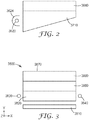
- FIG. 2 is a schematic side-view of a wedge-shape light guiding layer 3710, where the thickness decreases with increasing distance from lamp 3620.
- lightguide 3690 includes a light emitting surface 3695 that is a substantial portion of the top major surface of optical film 3640.
- light emitting surface 3695 includes at least about 50%, or at least about 60%, or at least about 70%, or at least about 80%, or at least about 90% of the top major surface of the optical film.
- uniformity of light emitted by the light emitting surface is not less than about 50%, or not less than about 60%, or not less than about 70%, or not less than about 80% across the light emitting surface, where uniformity is defined as the ratio of the minimum emitted light intensity to the maximum emitted light intensity times 100.
- Reflective polarizer layer 430 substantially reflects light that has a first polarization state and substantially transmits light that has a second polarization state, where the two polarization states are mutually orthogonal.
- the average reflectance of reflective polarizer 430 in the visible for light that is substantially reflected by the reflective polarizer is at least about 50%, or at least about 60%, or at least about 70%, or at least about 80%, or at least about 90%, or at least about 95%.
- the average transmittance of reflective polarizer 430 in the visible for light that is substantially transmitted by the reflective polarizer is at least about 50%, or at least about 60%, or at least about 70%, or at least about 80%, or at least about 90%, or at least about 95%, or at least about 97%, or at least about 98%, or at least about 99%.
- reflective polarizer 430 substantially reflects light having a first linear polarization state (for example, along the x-direction) and substantially transmits light having a second linear polarization state (for example, along the z-direction).
- reflective polarizer layer 430 may be used for reflective polarizer layer 430 such as, for example, a multilayer optical film (MOF) reflective polarizer, a diffusely reflective polarizing film (DRPF) having a continuous phase and a disperse phase, such as a VikuitiTM Diffuse Reflective Polarizer Film (“DRPF”) available from 3M Company, St. Paul, Minnesota, a wire grid reflective polarizer described in, for example, U.S. Patent No. 6,719,426 , or a cholesteric reflective polarizer.
- MOF multilayer optical film
- DRPF diffusely reflective polarizing film
- DRPF Diffuse Reflective Polarizer Film
- reflective polarizer layer 430 can be or include an MOF reflective polarizer, formed of alternating layers of different polymer materials, where one of the sets of alternating layers is formed of a birefringent material, where the refractive indices of the different materials are matched for light polarized in one linear polarization state and unmatched for light in the orthogonal linear polarization state.
- an incident light in the matched polarization state is substantially transmitted through reflective polarizer layer 430 and an incident light in the unmatched polarization state is substantially reflected by reflective polarizer layer 430.
- an MOF reflective polarizer layer 430 can include a stack of inorganic dielectric layers.
- reflective polarizer layer 430 can be or include a partially reflecting layer that has an intermediate on-axis average reflectance in the pass state.
- the partially reflecting layer can have an on-axis average reflectance of at least about 90% for visible light polarized in a first plane, such as the xy-plane, and an on-axis average reflectance in a range from about 25% to about 90% for visible light polarized in a second plane, such as the xz-plane, perpendicular to the first plane.
- Such partially reflecting layers are described in, for example, U.S. Patent Publication No. 2008/064133 .
- reflective polarizer layer 430 can be or include a circular reflective polarizer, where light circularly polarized in one sense, which may be the clockwise or counterclockwise sense (also referred to as right or left circular polarization), is preferentially transmitted and light polarized in the opposite sense is preferentially reflected.
- a circular polarizer includes a cholesteric liquid crystal polarizer.
- layer 430 can be a non-polarizing partial reflector.
- layer 430 can include a partially reflective metal and/or dielectric layer.
- layer 430 can have a structured surface.
- Liquid crystal panel 3670 includes, not expressly shown in FIG. 1 , a layer of liquid crystal disposed between two panel plates, an upper light absorbing polarizer layer disposed above the liquid crystal layer, and a lower absorbing polarizer disposed below the liquid crystal layer.
- the upper and lower light absorbing polarizers and the liquid crystal layer in combination, control the transmission of light from reflective polarizer layer 430 through liquid crystal panel 3670 to a viewer facing the display system.
- Back reflector 3605 can be any type reflector that may be desirable and/or practical in an application.
- the back reflector can be a specular reflector, a semi-specular or semi-diffuse reflector, or a diffuse reflector, such as those disclosed in International Patent Application No. PCT/US 2008/064115 , claiming priority from Provisional U.S. Patent Application No. 60/939085, filed May 20, 2007 .
- the reflector can be an aluminized film or a multi-layer polymeric reflective film, such as an enhanced specular reflector (ESR) film (available from 3M Company, St. Paul, MN).
- ESR enhanced specular reflector
- back reflector 3605 can be a diffuse reflector having a white appearance.
- Back reflector 3605 is proximate major bottom surface 3609 of light guiding layer 3610. Back reflector 3605 reflects light that exits the guiding layer from surface 3609 back toward lightguide 3690. In some cases, the back reflector is partially reflective and partially transmissive. In some cases, the back reflector can be structured, for example, have a structured surface.
- Optical adhesive layer 3650 can be any optical adhesive that may be desirable and/or available in an application. Optical adhesive layer 3650 is of sufficient optical quality and light stability such that, for example, the adhesive layer does not yellow with time or upon exposure to weather so as to degrade the optical performance of the adhesive and the optical film. In some cases, optical adhesive layer 3650 can be a substantially clear optical adhesive meaning that the adhesive layer has a high specular transmittance and a low diffuse transmittance. For example, in such cases, the specular transmittance of optical adhesive layer 3650 is at least about 70%, or at least about 80%, or at least about 90%, or at least about 95%.
- optical adhesive layer 3650 can be a substantially diffuse optical adhesive, meaning that the adhesive layer has a high diffuse transmittance and a low specular transmittance.
- the diffuse transmittance of optical adhesive layer 3650 is at least about 60%, or at least about 70%, or at least about 80%.
- optical adhesive layer 3650 can be a substantially polarization-preserving diffuse adhesive.
- Exemplary optical adhesives include pressure sensitive adhesives (PSAs), heat-sensitive adhesives, solvent-volatile adhesives, and UV-curable adhesives such as UV-curable optical adhesives available from Norland Products, Inc.
- PSAs pressure sensitive adhesives
- heat-sensitive adhesives heat-sensitive adhesives
- solvent-volatile adhesives solvent-volatile adhesives
- UV-curable adhesives such as UV-curable optical adhesives available from Norland Products, Inc.
- Exemplary PSAs include those based on natural rubbers, synthetic rubbers, styrene block copolymers, (meth)acrylic block copolymers, polyvinyl ethers, polyolefins, and poly(meth)acrylates.
- (meth)acrylic (or acrylate) refers to both acrylic and methacrylic species.
- Other exemplary PSAs include (meth)acrylates, rubbers, thermoplastic elastomers, silicones, urethanes, and combinations thereof. In some cases, the PSA is based on a (meth)acrylic PSA or at least one poly(meth)acrylate.
- Exemplary silicone PSAs include a polymer or gum and an optional tackifying resin.
- Other exemplary silicone PSAs include a polydiorganosiloxane polyoxamide and an optional tackifier.
- optical film 3640 substantially extends the entire light emitting surface 3695. According to the invention, the optical film covers only a portion of the light emitting surface.
- FIG. 11 is a schematic side-view of a lightguide 1100 that includes an optical film 1110 disposed only on a portion of major surface 3614 of light guiding layer 3610.
- light extraction features 1120 are disposed on another portion of major surface 3614.
- Optical film 1110 can be similar to optical film 3640.
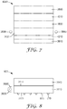
- FIG. 8 is a schematic side-view of a lightguide 800 that includes light guiding layer 3610, optical film 3640 disposed on top major surface 3614 of the light guiding layer and light extraction means 810 disposed on bottom major surface 3609 of the light guiding layer.
- Light extraction means 810 includes a plurality of discrete light extraction features 815.
- Optical film 3640 is the first light extracting means in lightguide 800, and light extraction features 815 are the second light extracting means in the lightguide.
- second light extraction means 810 can be any extraction means that may be desirable in an application.
- Light extraction means 810 can be a roughened bottom major surface 3609.
- Light extraction features 815 can be printed dots or extraction features, such as lenslets, where, in some cases, the extraction features can be integral to light guiding layer 3610.
- Light extraction means 810 can be an optical film similar to optical film 3640.
- FIG. 9 is a schematic side-view of a lightguide 900 that includes a second optical film 910 disposed on bottom major surface 3609, and between light guiding layer 3610 and back reflector 3605.
- back reflector 3605 is attached to optical film 910 by coating the optical film on the back reflector or lamination the back reflector to the optical film.
- Lightguide 900 emits light through top major surface 3614 and bottom major surface 3609. Light that is emitted downward through surface 3609 is reflected back in the upward direction by back reflector 3605.
- FIG. 10 is a schematic side-view of a display system 1000 that includes a lightguide 1050 disposed between a first liquid crystal panel 1030 and a second liquid crystal panel 1040.
- Lightguide 1050 emits light 1010 for illuminating liquid crystal panel 104 and light 1020 for illuminating liquid crystal panel 1030.
- the backlight 3680 includes a reflective polarizer layer laminated to optical film 3650 via optical adhesive layer 3650.
- backlight 3680 can include one or more light management films such as, a reflective polarizer, a light redirecting film such as a brightness enhancement film (for example, BEF available from 3M Company, Saint Paul MN), a turning film (for example, an inverted BEF), an optical diffuser, or any other light management film that may be desirable in an application.
- a reflective polarizer such as a reflective polarizer, a light redirecting film such as a brightness enhancement film (for example, BEF available from 3M Company, Saint Paul MN), a turning film (for example, an inverted BEF), an optical diffuser, or any other light management film that may be desirable in an application.
- a light redirecting film such as a brightness enhancement film (for example, BEF available from 3M Company, Saint Paul MN), a turning film (for example, an inverted BEF), an optical diffuser, or any other light management film that may be
- reflective polarizer 430 can be replaced with a prismatic brightness enhancement film, a light management film that includes a plurality of linear cylindrical lenses, or a light management film that includes a plurality of particles, such as spherical particles, disposed on a surface.
- light guiding layer 3610 receives light from two edges or sides 3611 and 3612.
- the light guiding layer can receive light from any number of edges or sides, such as from one, two, three, or four edges or sides.
- one or more edges of the light guiding layer that do not receive light can be made reflective to prevent optical loss.
- an optically diffusive film that may have a white appearance, can be attached to such an edge to reflect light that would otherwise exit the guiding layer back for extraction toward the emitting surface.
- one or more light receiving edges of light guiding layer 3610 can include surface features, such as molded surface structures, to spread the light that enters the light guiding layer from the lamps.
- edge 3612 includes surface features 3671 for spreading light 3632 inside the light guiding layer.
- Light guiding layer 3610 can be made of any optical material that may be desirable in an application, such as for example, any glass or any polymer that may be desirable in an application.
- light guiding layer 3610 can be made of polycarbonate, acrylic, or cyclo olefin polymer (COP) (for example, available from Zeon chemicals L.O., Louisville, KY).
- COP cyclo olefin polymer
- Backlight 3680 can have any shape or form that may be desirable in an application.
- the backlight can have a square shape, or a rectangular shape, or a circular shape.
- the edges of light guiding layer can be straight or curved.
- backlight 3680 can be planar or curved.
- Lamps 3620 and 3630 can be any type lamp that may be desirable in an application.
- the lamps can be extended diffuse sources such as cold cathode fluorescent lamps (CCFLs), smaller area solid state light sources such as light emitting diodes (LEDs), or lasers.
- CCFLs cold cathode fluorescent lamps
- LEDs light emitting diodes
- lasers lasers
- Backlight or light source 3680 can be used in any desirable application.
- Exemplary applications include signage, displays such as liquid crystal displays, luminaires, and license plates.
- Backlight 3680 can be produced using any fabrication method that may be desirable in an application.
- an optical film 1210 is coated on a low loss substrate 1205 as shown schematically in FIG. 12A .
- Optical film 1210 can be any optical film disclosed herein.
- optical film 1210 can be similar to optical film 3640.
- the construction in FIG. 12A is cut to a desired size and shape and one or more of the edges are polished as shown schematically in FIG. 12B . Edges 1220 and 1225 have been polished.
- a reflective film 1230 is attached, such as laminated, to edge 1225.
- FIG. 12C a reflective film 1230 is attached, such as laminated, to edge 1225.
- a lamp 1240 is disposed along edge 1220 of the substrate and a back reflector 1250 is disposed approximate major back surface 1260 of substrate 1205.
- substrate 1202 is the guiding layer and optical film 1210 provides TIR and light extraction means.
- the display system 3600 includes a single display system.
- a display system can include one or more displays.
- FIG. 13 is a schematic top-view of a display system 1300 that displays an image and includes a plurality of discrete displays 1310.
- Each discrete display 1310 can be individually controlled.
- the output light intensity of each discrete display can be individually controlled, meaning that the output intensity of one discrete display can be changed without changing the output intensities of the other discrete displays.
- At least one of the discrete displays includes or is display system 3600.
- at least one discrete display 1310 includes a backlight disclosed herein, such as backlight 3680.
- each discrete display 1310 displays a different portion of the image that is displayed by display system 1300.
- a coating solution "A” was made.
- a "906" composition (available from 3M Company, St. Paul, Minnesota) was obtained.
- the 906 composition included: 18.4 wt % 20 nm silica particles (Nalco 2327) surface modified with methacryloyloxypropyltrimethoxysilane (acrylate silane), 25.5 wt % Pentaerthritol tri/tetra acrylate (PETA), 4.0 wt % N,N-dimethylacrylamide (DMA), 1.2 wt % Irgacure 184, 1.0 wt % Tinuvin 292 , 46.9 wt % solvent isopropanol, and 3.0 wt % water.
- the 906 composition was approximately 50% solid by weight.
- the 906 composition was diluted to 35 wt% solid with solvent 1-methoxy 2-propanol resulting in coating solution A.
- a coating solution "B” was made. First, 360 g of Nalco 2327 colloidal silica particles (40% wt solid and an average particle diameter of about 20 nanometers) (available from Nalco Chemical Company, Naperville IL) and 300 g of solvent 1-methoxy-2-propanol were mixed together under rapid stirring in a 2-liter three-neck flask that was equipped with a condenser and a thermometer. Next, 22.15 g of Silquest A-174 silane (available from GE Advanced Materials, Wilton CT) was added. The mixture was stirred for 10 min. Next, an additional 400 g of 1-methoxy-2-propanol was added. The mixture was heated at 85 °C for 6 hours using a heating mantle.
- the resulting solution was allowed to cool down to room temperature. Next, most of water and 1-methoxy-2-propanol solvents (about 700 g) were removed using a rotary evaporator under a 60 °C water-bath. The resulting solution was 44% wt A-174 modified 20 nm silica clear dispersed in 1-methoxy-2-propanol. Next, 70.1 g of this solution, 20.5 g of SR 444 (available from Sartomer Company, Exton PA), 1.375 g of photoinitiator Irgacure 184 (available from Ciba Specialty Chemicals Company, High Point NC), and 80.4 g of isopropyl alcohol were mixed together by stirring to form a homogenous coating solution B.
- SR 444 available from Sartomer Company, Exton PA
- Irgacure 184 available from Ciba Specialty Chemicals Company, High Point NC
- 80.4 g of isopropyl alcohol were mixed together by stirring to form a
- a coating solution "C” was made. First, 309 g of Nalco 2327 (40% wt solid) and 300 g of 1-methoxy-2-propanol were mixed together under rapid stirring in a 2-liter three-neck flask that was equipped with a condenser and a thermometer. Next, 9.5 g of Silquest A-174 and 19.0 g of Siquest A-1230 were added, and the resulting mixture was stirred for 10 min. The mixture was heated at 80 °C for 1 hour using a heating mantle. Next, an additional 400 g of 1-mothoxy-2-propanol was added. The mixture was kept at 80°C for 16 hours. The resulting solution was allowed to cool down to room temperature.
- a coating solution "D" was made. 300 g of Nalco 2329 silica particles (40% wt solid) (with an average particle size of 75 nm, available from Nalco Chemical Company, Naperville IL) and 300 g of 1-methoxy-2-propanol were mixed together under rapid stirring in a 1-liter flask that was equipped with a condenser and a thermometer. Next, 7.96 g of Silquest A-174 was added. The resulting mixture was stirred for 10 min. Next, an additional 400 g of 1-methoxy-2-propanol was added. The resulting mixture was heated at 85 °C for 6 hours using a heating mantle. The resulting solution was allowed to cool down to room temperature.
- a coating procedure "E” was developed. First, a coating solution was syringe-pumped at a rate of 3 cc/min into a 10.2 cm (4-inch) wide slot-type coating die. The slot coating die uniformly distributed a 10.2 cm wide coating onto a substrate moving at 5 ft/min (152 cm/min).
- the coating was polymerized by passing the coated substrate through a UV-LED cure chamber that included a quartz window to allow passage of UV radiation.
- the UV-LED bank included a rectangular array of 160 UV-LEDs, 8 down-web by 20 cross-web (approximately covering a 10.2 cm x 20.4 cm area).
- the LEDs (available from Cree, Inc., Durham NC) operated at a nominal wavelength of 385 nm, and were run at 45 Volts at 8 Amps, resulting in a UV-A dose of 0.212 joules per square cm.
- the UV-LED array was powered and fan-cooled by a TENMA 72-6910 (42V/10A) power supply (available from Tenma, Springboro OH).
- the UV-LEDs were positioned above the quartz window of the cure chamber at a distance of approximately 2.54 cm from the substrate.
- the UV-LED cure chamber was supplied with a flow of nitrogen at a flow rate of 46.7 liters/min (100 cubic feet per hour) resulting in an oxygen concentration of approximately 150 ppm in the cure chamber.
- the solvent in the cured coating was removed by transporting the coated substrate to a drying oven at 150 °F for 2 minutes at a web speed of 5 ft/min.
- the dried coating was post-cured using a Fusion System Model I300P configured with an H-bulb (available from Fusion UV Systems, Gaithersburg MD).
- the UV Fusion chamber was supplied with a flow of nitrogen that resulted in an oxygen concentration of approximately 50 ppm in the chamber.
- a coating procedure "F” was developed. First, a coating solution was syringe-pumped at a rate of 2.7 cc/min into a 20.3 cm (8-inch) wide slot-type coating die. The slot coating die uniformly distributed a 20.3 cm wide coating onto a substrate moving at 5ft/min (152 cm/min).
- the coating was polymerized by passing the coated substrate through a UV-LED cure chamber that included a quartz window to allow passage of UV radiation.
- the UV-LED bank included a rectangular array of 352 UV-LEDs, 16 down-web by 22 cross-web (approximately covering a 20.3 cm x 20.3 cm area).
- the UV-LEDs were placed on two water-cooled heat sinks.
- the LEDs available from Cree, Inc., Durham NC) operated at a nominal wavelength of 395 nm, and were run at 45 Volts at 10 Amps, resulting in a UV-A dose of 0.108 joules per square cm.
- the UV-LED array was powered and fan-cooled by a TENMA 72-6910 (42V/10A) power supply (available from Tenma, Springboro OH).
- the UV-LEDs were positioned above the cure chamber quartz window at a distance of approximately 2.54 cm from the substrate.
- the UV-LED cure chamber was supplied with a flow of nitrogen at a flow rate of 46.7 liters/min (100 cubic feet per hour) resulting in an oxygen concentration of approximately 150 ppm in the cure chamber.
- the solvent in the cured coating was removed by transporting the coating to a drying oven operating at 150 °F for 2 minutes at a web speed of 5 ft/min.
- the dried coating was post-cured using a Fusion System Model I300P configured with an H-bulb (available from Fusion UV Systems, Gaithersburg MD).
- the UV Fusion chamber was supplied with a flow of nitrogen that resulted in an oxygen concentration of approximately 50 ppm in the chamber.
- Backlight 3800 included a back reflector 3810, a lightguide 3820, lamps 3830 and 3840, and a reflective polarizer layer 3860 laminated to the backlight with an optical adhesive layer 3850.
- Reflective polarizer layer 3860 had a pass axis along the z-axis.
- the average on-axis (along the y-direction) reflectivity of the reflecting polarizer layer for incident light polarized along the z-axis (the pass axis) was about 68%, and the average on-axis (along the y-direction) reflectivity of the reflecting polarizer layer for incident light polarized along the x-axis (the block axis) was about 99.2%.
- the reflective polarizer layer was made as described in International Publication No. WO 2008/144656 .
- the reflective polarizer layer included 274 alternating microlayers of birefringent 90/10 coPEN material and Eastman Neostar Elastomer FN007 (available from Eastman Chemical, Kingsport TN).
- the 274 alternating microlayers were arranged in a sequence of 1 ⁇ 4 wave layer pairs, where the thickness gradient of the layers was designed to provide a strong reflection resonance broadly and uniformly across a bandwidth from approximately 400 nm to 1050 nm for one polarization axis, and a weaker reflection resonance broadly and uniformly across a bandwidth from approximately 400 nm to 900 nm for the orthogonal axis.
- Two 5 micron ( ⁇ m) thick skin layers of PET-G were disposed on the outside surfaces of the coherent altering microlayer stack.
- the overall thickness of the reflective polarizer layer was approximately 40 microns ( ⁇ m).
- Optical adhesive layer 3850 was optically clear adhesive OCA 1873 available from 3M.
- Lightguide 3820 was a unitary solid light. The lightguide was about 6 mm thick (y-direction), 472 mm wide (z-direction), and 306 mm long (x-direction).
- Back reflector 3810 is an ESR film available from 3M. There was a small air gap between the solid lightguide and the back reflector. Each of lamps 3830 and 3840 included 78 LEDs placed near a corresponding edge of the solid lightguide and arranged regularly along the width of the solid lightguide.
- the luminance distribution as a function of viewing angle, axial luminance (in units of nits), the half-luminance angle (in the xy-plane), and the extinction ratio of lightguide 3800 was measured using an Autronic Conoscope Conostage 3 (available from Autronic-Melchers GmbH, Düsseldorf, Germany).
- Autronic Conoscope Conostage 3 available from Autronic-Melchers GmbH, Düsseldorf, Germany.
- a linear absorbing polarizer not shown expressly in FIG. 3 , was placed on top of the reflective polarizer layer with its pass-axis parallel to the pass-axis of the reflective polarizer.
- the extinction ratio was I 1 /I 2 , where I 1 was the measured axial luminance when the two pass-axes were parallel, and I 2 was the measured axial luminance when the two pass-axes were crossed.
- Brightness uniformity of backlight 3800 was measured by recording the on-axis luminance of the backlight at 13 different locations as illustrated in FIG. 4 .
- FIG. 4 is a schematic top-view of backlight 3800, where the 13 measurement points 3910 are the locations at which on-axis brightness of the backlight were measured.
- Surface 3870 is the top surface of reflective polarizer layer 3860.
- the S 1 /S, S 2 /S, S 3 /S, S 4 /S, and S 5 /S were 0.1, 0.3, 0.5, 0.7, and 0.9, respectively, where S was the length of the lightguide (472 mm).
- FIG. 6A is a grayscale conoscopic image of the measured luminance of backlight 3800 as a function of viewing angle.
- the grid overlaying the image is provided for reference purposes to show the azimuthal angle ⁇ ranging from 0 to 360 degrees, and the polar angle ⁇ ranging from 0 at the center to more than 80 degrees at the periphery, with concentric circles provided for each 20 degree increment of ⁇ .
- Table I Optical performance properties in Examples 1-6 Example No.
- Backlight 4000 was similar to backlight 3800 except that an optical film 4010 was disposed between optical adhesive layer 3850 and reflective polarizer layer 3860.
- Optical film 4010 was made by coating solution B from Example B on reflective polarizer layer 3860 (the same as the reflective polarizer in Example 1) using the coating method described in Example F, except that the syringe pump rate was 6 cc/min and the LEDs were run at 13 Amps (resulting in a UV-A dose of 0.1352 joules per square cm).
- the index of the resulting optical film was about 1.22.
- the optical haze of the optical film was 9%.
- the thickness of the optical film was about 5 microns ( ⁇ m).
- optically clear adhesive OCA 1873 layer 3850 was used to laminate the optical film to lightguide 3820. Measurements similar to those described in Example 1 were made and are summarized in Table I.
- FIG. 6B is a grayscale conoscopic image of the measured luminance of the backlight as a function of viewing angle.
- a backlight 4000 was made.
- the backlight was similar to the backlight made in Example 2, except that optical film 4010 was made by coating solution C from Example C on reflective polarizer layer 3860 (the same as the reflective polarizer in Example 1) using the coating method described in Example F, except that the syringe pump rate was 1.5 cc/min and the LEDs were run at 13 Amps (resulting in a UV-A dose of 0.1352 joules per square cm).
- the index of the resulting optical film was about 1.25.
- the optical haze of the optical film was 20%.
- the thickness of the optical film was about 5 microns ( ⁇ m).
- optically clear adhesive OCA 1873 layer 3850 was used to laminate the optical film to lightguide 3820. Measurements similar to those described in Example 1 were made and are summarized in Table I.
- FIG. 6C is a grayscale conoscopic image of the measured luminance of the backlight as a function of viewing angle.
- a backlight 4000 was made.
- the backlight was similar to the backlight made in Example 2, except that optical film 4010 was made by coating solution C from Example C on reflective polarizer layer 3860 (the same as the reflective polarizer in Example 1) using the coating method described in Example F, except that the LEDs were run at 9 Amps (resulting in a UV-A dose of 0.0936 joules per square cm).
- the index of the resulting optical film was about 1.18.
- the optical haze of the optical film was 40%.
- the thickness of the optical film was about 5 microns ( ⁇ m).
- optically clear adhesive OCA 1873 layer 3850 was used to laminate the optical film to lightguide 3820. Measurements similar to those described in Example 1 were made and are summarized in Table I.
- FIG. 6D is a grayscale conoscopic image of the measured luminance of the backlight as a function of viewing angle.
- a backlight 4000 was made.
- the backlight was similar to the backlight made in Example 2, except that optical film 4010 was made by coating solution C from Example C on reflective polarizer layer 3860 (the same as the reflective polarizer in Example 1) using the coating method described in Example F, except that the LEDs were run at 6 Amps (resulting in a UV-A dose of 0.0624 joules per square cm).
- the index of the resulting optical film was about 1.17.
- the optical haze of the optical film was 60%.
- the thickness of the optical film was about 5 microns ( ⁇ m).
- optically clear adhesive OCA 1873 layer 3850 was used to laminate the optical film to lightguide 3820. Measurements similar to those described in Example 1 were made and are summarized in Table I.
- FIG. 6E is a grayscale conoscopic image of the measured luminance of the backlight as a function of viewing angle.
- a backlight 4200 a schematic side-view of which is shown in FIG. 7 , was made.
- the backlight was similar to the backlight 4000 except that the back reflector 3810 was laminated to the bottom of lightguide 3820 using optical adhesive layer 4210.
- Reflective polarizer 3860 was the same as the reflective polarizer in Example 2.
- Back reflector 3810 was a multilayer polymeric mirror made with 550 alternating layers of PEN and PMMA. The back reflector had a reflection band extending from about 400 nm to about 1600 nm at normal incidence. The average reflectivity of the back reflector over that wavelength range was about 99%.
- Back reflector 3810 was laminated to lightguide 3820 using an optically clear adhesive OCA 1873 layer 4210.
- Optical film 4010 was made by coating solution D from Example D on reflective polarizer layer 3860 (the same as the reflective polarizer in Example 1) using the coating method described in Example F, except that the syringe flow rate was 2.3 cc/min and the UV LED current was 4 Amps (resulting in a UV-A dose of 0.0416 joules per square cm).
- the index of the resulting optical film was about 1.19.
- the optical haze of the optical film was 90%.
- the thickness of the optical film was about 5 microns ( ⁇ m).
- optically clear adhesive OCA 1873 layer 3850 was used to laminate the optical film to lightguide 3820. Measurements similar to those described in Example 1 were made and are summarized in Table I.
- FIG. 6F is a grayscale conoscopic image of the measured luminance of the backlight as a function of viewing angle.
Applications Claiming Priority (2)
| Application Number | Priority Date | Filing Date | Title |
|---|---|---|---|
| US16955509P | 2009-04-15 | 2009-04-15 | |
| PCT/US2010/030984 WO2010120845A2 (en) | 2009-04-15 | 2010-04-14 | Backlight and display system incorporating same |
Publications (2)
| Publication Number | Publication Date |
|---|---|
| EP2419771A2 EP2419771A2 (en) | 2012-02-22 |
| EP2419771B1 true EP2419771B1 (en) | 2020-09-23 |
Family
ID=42670363
Family Applications (1)
| Application Number | Title | Priority Date | Filing Date |
|---|---|---|---|
| EP10714528.6A Active EP2419771B1 (en) | 2009-04-15 | 2010-04-14 | Lightguide with optical film containing voids |
Country Status (6)
| Country | Link |
|---|---|
| US (1) | US8891038B2 (ko) |
| EP (1) | EP2419771B1 (ko) |
| JP (2) | JP2012524381A (ko) |
| KR (1) | KR101770837B1 (ko) |
| CN (1) | CN102460244B (ko) |
| WO (1) | WO2010120845A2 (ko) |
Families Citing this family (49)
| Publication number | Priority date | Publication date | Assignee | Title |
|---|---|---|---|---|
| CN102124384B (zh) * | 2008-07-10 | 2016-10-12 | 3M创新有限公司 | 粘弹性光导 |
| CN107037526A (zh) * | 2008-08-08 | 2017-08-11 | 3M创新有限公司 | 具有粘弹性层的用于控制光的光导 |
| US9464179B2 (en) | 2009-04-15 | 2016-10-11 | 3M Innovative Properties Company | Process and apparatus for a nanovoided article |
| EP2419767A1 (en) | 2009-04-15 | 2012-02-22 | 3M Innovative Properties Company | Optical film |
| TWI605276B (zh) | 2009-04-15 | 2017-11-11 | 3M新設資產公司 | 光學結構及包含該光學結構之顯示系統 |
| US9291752B2 (en) | 2013-08-19 | 2016-03-22 | 3M Innovative Properties Company | Retroreflecting optical construction |
| CN102460125B (zh) | 2009-04-15 | 2015-11-25 | 3M创新有限公司 | 防止光学耦合的光学膜 |
| KR101769171B1 (ko) | 2009-10-24 | 2017-08-17 | 쓰리엠 이노베이티브 프로퍼티즈 컴파니 | 광원 및 이를 포함하는 디스플레이 시스템 |
| JP5898085B2 (ja) | 2009-10-24 | 2016-04-06 | スリーエム イノベイティブ プロパティズ カンパニー | 低減した色を有する浸漬された非対称反射体 |
| US9279918B2 (en) | 2009-10-24 | 2016-03-08 | 3M Innovative Properties Company | Gradient low index article and method |
| EP2491440A4 (en) | 2009-10-24 | 2018-05-02 | 3M Innovative Properties Company | Voided diffuser |
| US9063293B2 (en) | 2009-10-24 | 2015-06-23 | 3M Innovative Properties Company | Immersed reflective polarizer with angular confinement in selected planes of incidence |
| JP2013508781A (ja) | 2009-10-24 | 2013-03-07 | スリーエム イノベイティブ プロパティズ カンパニー | 高い軸外反射率を有する浸漬した反射偏光子 |
| KR101781661B1 (ko) | 2009-10-24 | 2017-09-25 | 쓰리엠 이노베이티브 프로퍼티즈 컴파니 | 구배 나노공극형 물품을 위한 방법 |
| US8950924B2 (en) | 2009-12-08 | 2015-02-10 | 3M Innovative Properties Company | Optical constructions incorporating a light guide and low refractive index films |
| US8917447B2 (en) | 2010-01-13 | 2014-12-23 | 3M Innovative Properties Company | Microreplicated film for attachment to autostereoscopic display components |
| CN102822247B (zh) | 2010-04-14 | 2016-06-08 | 3M创新有限公司 | 图案化梯度聚合物膜和方法 |
| MX341955B (es) | 2010-04-15 | 2016-09-08 | 3M Innovative Properties Co | Articulos retrorreflectantes que incluyen areas opticamente activas y areas opticamente inactivas. |
| EP2558290B1 (en) | 2010-04-15 | 2019-01-23 | 3M Innovative Properties Company | Retroreflective articles including optically active areas and optically inactive areas |
| EP2558288B1 (en) | 2010-04-15 | 2019-01-02 | 3M Innovative Properties Company | Retroreflective articles including optically active areas and optically inactive areas |
| EP2630527A1 (en) | 2010-10-20 | 2013-08-28 | 3M Innovative Properties Company | Wide band semi-specular mirror film incorporating nanovoided polymeric layer |
| US8469551B2 (en) | 2010-10-20 | 2013-06-25 | 3M Innovative Properties Company | Light extraction films for increasing pixelated OLED output with reduced blur |
| US8547015B2 (en) | 2010-10-20 | 2013-10-01 | 3M Innovative Properties Company | Light extraction films for organic light emitting devices (OLEDs) |
| EP2678736B1 (en) * | 2011-02-25 | 2015-01-21 | 3M Innovative Properties Company | Variable index light extraction layer for use in a front-lit reflective display device |
| KR20140015443A (ko) | 2011-03-09 | 2014-02-06 | 쓰리엠 이노베이티브 프로퍼티즈 컴파니 | 입자 크기가 큰 건식 실리카를 포함하는 반사 방지 필름 |
| US9505028B2 (en) * | 2012-03-30 | 2016-11-29 | 3M Innovative Properties Company | Protective coating for low index material |
| US8915002B2 (en) * | 2013-01-31 | 2014-12-23 | 3M Innovative Properties Company | Self illuminated signage for printed graphics |
| KR20150115794A (ko) | 2013-02-08 | 2015-10-14 | 쓰리엠 이노베이티브 프로퍼티즈 컴파니 | 집적 양자점 광학 구조물 |
| US10222535B2 (en) | 2013-07-02 | 2019-03-05 | 3M Innovative Properties Company | Flat light guide |
| US8922895B1 (en) | 2013-07-03 | 2014-12-30 | 3M Innovative Properties Company | Optical body with fresnel-rendering of complex topographical surface |
| CN104456295B (zh) * | 2014-11-07 | 2018-01-16 | 深圳市华星光电技术有限公司 | 一种背光模组及喷涂治具 |
| US10723894B2 (en) | 2014-12-23 | 2020-07-28 | 3M Innovative Properties Company | Tie layers prepared from particle-containing waterborne suspensions |
| JP6612563B2 (ja) | 2014-12-26 | 2019-11-27 | 日東電工株式会社 | シリコーン多孔体およびその製造方法 |
| JP6563750B2 (ja) | 2014-12-26 | 2019-08-21 | 日東電工株式会社 | 塗料およびその製造方法 |
| JP6604781B2 (ja) | 2014-12-26 | 2019-11-13 | 日東電工株式会社 | 積層フィルムロールおよびその製造方法 |
| JP6599699B2 (ja) | 2014-12-26 | 2019-10-30 | 日東電工株式会社 | 触媒作用を介して結合した空隙構造フィルムおよびその製造方法 |
| JP6713872B2 (ja) | 2015-07-31 | 2020-06-24 | 日東電工株式会社 | 積層フィルム、積層フィルムの製造方法、光学部材、画像表示装置、光学部材の製造方法および画像表示装置の製造方法 |
| JP6713871B2 (ja) | 2015-07-31 | 2020-06-24 | 日東電工株式会社 | 光学積層体、光学積層体の製造方法、光学部材、画像表示装置、光学部材の製造方法および画像表示装置の製造方法 |
| JP6892744B2 (ja) | 2015-08-24 | 2021-06-23 | 日東電工株式会社 | 積層光学フィルム、積層光学フィルムの製造方法、光学部材、および画像表示装置 |
| JP7152130B2 (ja) | 2015-09-07 | 2022-10-12 | 日東電工株式会社 | 低屈折率層、積層フィルム、低屈折率層の製造方法、積層フィルムの製造方法、光学部材および画像表示装置 |
| CN109312910B (zh) * | 2016-06-10 | 2020-01-07 | 3M创新有限公司 | 包括结构化反射器的再循环背光源 |
| US20190302530A1 (en) * | 2016-06-10 | 2019-10-03 | 3M Innovative Properties Company | Recycling backlight |
| JP6723128B2 (ja) * | 2016-09-27 | 2020-07-15 | 東京エレクトロン株式会社 | ニッケル配線の製造方法 |
| CN110268192B (zh) * | 2017-01-26 | 2021-03-16 | 3M创新有限公司 | 显示系统 |
| CN106842408A (zh) * | 2017-03-31 | 2017-06-13 | 京东方科技集团股份有限公司 | 导光板、制备导光板的方法以及显示装置 |
| EP3770648A4 (en) * | 2018-03-22 | 2022-01-05 | Tokuyama Corporation | PROCESS FOR PRODUCING A PLASTIC LENS WITH A COATING LAYER |
| US20220041781A1 (en) * | 2018-12-17 | 2022-02-10 | Agency For Science, Technology And Research | A Polymer Composition and a Method of Preparing a Polymer Resin |
| CN114174807A (zh) | 2019-07-26 | 2022-03-11 | 3M创新有限公司 | 多孔流体传感器 |
| KR20240011533A (ko) * | 2022-07-19 | 2024-01-26 | 주식회사 창강화학 | 광학 필름 및 이를 포함하는 백라이트 유닛 |
Citations (2)
| Publication number | Priority date | Publication date | Assignee | Title |
|---|---|---|---|---|
| US5919555A (en) * | 1996-11-06 | 1999-07-06 | Fuji Photo Film Co., Ltd. | Anti-reflection film and display device having the same |
| US20030123150A1 (en) * | 2001-12-14 | 2003-07-03 | Eastman Kodak Company | Microvoided light diffuser |
Family Cites Families (153)
| Publication number | Priority date | Publication date | Assignee | Title |
|---|---|---|---|---|
| US3924929A (en) | 1966-11-14 | 1975-12-09 | Minnesota Mining & Mfg | Retro-reflective sheet material |
| FR1566455A (ko) | 1968-03-01 | 1969-05-09 | ||
| US3712706A (en) | 1971-01-04 | 1973-01-23 | American Cyanamid Co | Retroreflective surface |
| GB1476447A (en) | 1974-10-28 | 1977-06-16 | Minnesota Mining & Mfg | Reflector sturcture |
| US4127693A (en) | 1975-02-10 | 1978-11-28 | Lemelson Jerome H | Reflex reflectors with pyramid-shaped indentations |
| US4025159A (en) | 1976-02-17 | 1977-05-24 | Minnesota Mining And Manufacturing Company | Cellular retroreflective sheeting |
| US4202600A (en) | 1978-04-24 | 1980-05-13 | Avery International Corporation | Diced retroreflective sheeting |
| US4243618A (en) | 1978-10-23 | 1981-01-06 | Avery International Corporation | Method for forming retroreflective sheeting |
| US4539256A (en) | 1982-09-09 | 1985-09-03 | Minnesota Mining And Manufacturing Co. | Microporous sheet material, method of making and articles made therewith |
| US4478769A (en) | 1982-09-30 | 1984-10-23 | Amerace Corporation | Method for forming an embossing tool with an optically precise pattern |
| US5156863A (en) | 1982-09-30 | 1992-10-20 | Stimsonite Corporation | Continuous embossing belt |
| US4588258A (en) | 1983-09-12 | 1986-05-13 | Minnesota Mining And Manufacturing Company | Cube-corner retroreflective articles having wide angularity in multiple viewing planes |
| ZA847338B (en) | 1983-09-19 | 1985-05-29 | Amerace Corp | Retroreflective sheeting and methods for making same |
| US4672089A (en) | 1984-08-10 | 1987-06-09 | Amerace Corporation | Retroreflective sheeting |
| US4618518A (en) | 1984-08-10 | 1986-10-21 | Amerace Corporation | Retroreflective sheeting and methods for making same |
| US4656072A (en) | 1985-06-17 | 1987-04-07 | Coburn Corporation | Retroreflective material for providing a colored decorative effect in visible light |
| CA1279783C (en) | 1985-11-21 | 1991-02-05 | Minnesota Mining And Manufacturing Company | Totally internally reflecting thin, flexible film |
| US5056892A (en) | 1985-11-21 | 1991-10-15 | Minnesota Mining And Manufacturing Company | Totally internally reflecting thin, flexible film |
| US4726706A (en) | 1986-06-02 | 1988-02-23 | Attar Adil H | Reflective pavement marker |
| US4775219A (en) | 1986-11-21 | 1988-10-04 | Minnesota Mining & Manufacturing Company | Cube-corner retroreflective articles having tailored divergence profiles |
| US4726989A (en) | 1986-12-11 | 1988-02-23 | Minnesota Mining And Manufacturing | Microporous materials incorporating a nucleating agent and methods for making same |
| US4801193A (en) | 1988-03-04 | 1989-01-31 | Reflexite Corporation | Retroreflective sheet material and method of making same |
| US5120594A (en) | 1989-11-20 | 1992-06-09 | Minnesota Mining And Manufacturing Company | Microporous polyolefin shaped articles with patterned surface areas of different porosity |
| US5238623A (en) | 1989-11-20 | 1993-08-24 | Minnesota Mining And Manufacturing Company | Method for preparing microporous polyolefin shaped articles |
| US5229882A (en) | 1990-05-16 | 1993-07-20 | Reflexite Corporation | Colored retroreflective sheeting and method of making same |
| CA2064484C (en) | 1991-04-11 | 1998-08-11 | William P. Rowland | Retroreflective sheet |
| US5528720A (en) | 1992-03-23 | 1996-06-18 | Minnesota Mining And Manufacturing Co. | Tapered multilayer luminaire devices |
| US6002829A (en) | 1992-03-23 | 1999-12-14 | Minnesota Mining And Manufacturing Company | Luminaire device |
| US5831766A (en) | 1993-02-17 | 1998-11-03 | Reflexite Corporation | Retroreflective structure |
| CA2099067C (en) | 1993-06-23 | 2001-02-13 | Makoto Oe | Plane light source unit |
| US5759468A (en) | 1993-10-20 | 1998-06-02 | Minnesota Mining And Manufacturing Company | Raised zone retroreflective cube corner article and method of manufacture |
| US5614286A (en) | 1993-10-20 | 1997-03-25 | Minnesota Mining And Manufacturing Company | Conformable cube corner retroreflective sheeting |
| US5691846A (en) | 1993-10-20 | 1997-11-25 | Minnesota Mining And Manufacturing Company | Ultra-flexible retroreflective cube corner composite sheetings and methods of manufacture |
| WO1995011469A2 (en) | 1993-10-20 | 1995-04-27 | Minnesota Mining And Manufacturing Company | Directly machined raised structure retroreflective cube corner article and method of manufacture |
| US5450235A (en) | 1993-10-20 | 1995-09-12 | Minnesota Mining And Manufacturing Company | Flexible cube-corner retroreflective sheeting |
| US5804610A (en) | 1994-09-09 | 1998-09-08 | Minnesota Mining And Manufacturing Company | Methods of making packaged viscoelastic compositions |
| US5591527A (en) | 1994-11-02 | 1997-01-07 | Minnesota Mining And Manufacturing Company | Optical security articles and methods for making same |
| US5814565A (en) | 1995-02-23 | 1998-09-29 | University Of Utah Research Foundation | Integrated optic waveguide immunosensor |
| KR19990007929A (ko) | 1995-04-26 | 1999-01-25 | 데이빗로스클리블랜드 | 다면 반복 노광 방법 및 장치 |
| US6143224A (en) | 1995-05-18 | 2000-11-07 | Reflexite Corporation | Method for forming a retroreflective sheeting |
| BR9609314A (pt) | 1995-06-26 | 1999-07-06 | Minnesota Mining & Mfg | Película de multicamadas |
| US6139158A (en) | 1995-07-26 | 2000-10-31 | Reflexite Corporation | Retroreflective articles with multiple size prisms in multiple locations |
| CN1113268C (zh) | 1995-09-22 | 2003-07-02 | 皇家菲利浦电子有限公司 | 平板图像显示装置 |
| CN1147742C (zh) | 1995-11-02 | 2004-04-28 | 美国3M公司 | 具有背衬的立方角逆向反射片及其制造方法 |
| US20030170426A1 (en) | 1995-12-01 | 2003-09-11 | W. Scott Thielman | Cellular retroreflective sheeting |
| US6383559B1 (en) | 1995-12-07 | 2002-05-07 | Fuji Photo Film Co., Ltd. | Anti-reflection film and display device having the same |
| US5882796A (en) | 1996-04-01 | 1999-03-16 | Minnesota Mining And Manufacturing Company | Bonded structured retroreflective sheeting |
| US6355759B1 (en) | 1996-04-25 | 2002-03-12 | 3M Innovative Properties Company | Polydiorganosiloxane polyurea segmented copolymers and a process for making same |
| US6210858B1 (en) | 1997-04-04 | 2001-04-03 | Fuji Photo Film Co., Ltd. | Anti-reflection film and display device using the same |
| US5992066A (en) | 1997-04-21 | 1999-11-30 | Brauer; William R. | Apparatus with laminated diffuser for illuminating medical diagnostic imaging film |
| US5993954A (en) | 1997-04-29 | 1999-11-30 | 3M Innovative Properties Company | Temperature-sensitive microporous film |
| US6224223B1 (en) | 1997-12-22 | 2001-05-01 | Casio Computer Co., Ltd. | Illumination panel and display device using the same |
| US6090861A (en) | 1998-12-28 | 2000-07-18 | General Ideas, Inc. | Process for high temperature production of organic aerogels |
| US6132861A (en) | 1998-05-04 | 2000-10-17 | 3M Innovatives Properties Company | Retroreflective articles including a cured ceramer composite coating having a combination of excellent abrasion, dew and stain resistant characteristics |
| DE69938086T2 (de) | 1998-06-05 | 2009-01-29 | Fujifilm Corporation | Antireflektionsschicht und Anzeigegerät mit dieser Schicht |
| US6287670B1 (en) | 1999-01-11 | 2001-09-11 | 3M Innovative Properties Company | Cube corner cavity based retroreflectors and methods for making same |
| US6967053B1 (en) | 1999-01-21 | 2005-11-22 | Reflexite Corporation | Durable, open-faced retroreflective prismatic construction |
| US6224792B1 (en) | 1999-04-13 | 2001-05-01 | 3M Innovative Properties Company | Cutting and edge sealing cellular retroreflective sheeting |
| US6204202B1 (en) | 1999-04-14 | 2001-03-20 | Alliedsignal, Inc. | Low dielectric constant porous films |
| DE19929591A1 (de) | 1999-06-28 | 2001-01-04 | Max Planck Gesellschaft | Herstellung von epitaktischen GaN-Schichten auf Substraten |
| US6461724B1 (en) | 1999-08-30 | 2002-10-08 | 3M Innovative Properties Company | Microporous material resistant to capillary collapse |
| US6677028B1 (en) | 1999-09-10 | 2004-01-13 | 3M Innovative Properties Company | Retroreflective articles having multilayer films and methods of manufacturing same |
| US6573305B1 (en) | 1999-09-17 | 2003-06-03 | 3M Innovative Properties Company | Foams made by photopolymerization of emulsions |
| ATE391303T1 (de) | 1999-09-28 | 2008-04-15 | Fujifilm Corp | Antireflexbeschichtung, damit versehene polarisationsplatte, und bildanzeigegerät mit der antireflexbeschichtung oder mit der polarisationsplatte |
| KR100843639B1 (ko) | 1999-10-19 | 2008-07-07 | 롤리크 아게 | 위상 구조화 중합체 필름 또는 피막의 제조방법, 당해 방법으로부터 제조된 필름 또는 피막, 및 당해 필름 또는 피막을 포함하는 광학 제품 |
| US6376590B2 (en) | 1999-10-28 | 2002-04-23 | 3M Innovative Properties Company | Zirconia sol, process of making and composite material |
| US6325515B1 (en) | 2000-03-21 | 2001-12-04 | 3M Innovative Properties Company | Cube corner retroreflective article with enhanced pigmentation |
| JP2001337207A (ja) | 2000-03-21 | 2001-12-07 | Sumitomo Chem Co Ltd | 前方散乱シート、それを用いた積層シート及び液晶表示装置 |
| JP4028155B2 (ja) | 2000-04-11 | 2007-12-26 | 日本カーバイド工業株式会社 | 蛍光性再帰反射シート |
| AU2001274008A1 (en) | 2000-05-19 | 2001-12-03 | Koninklijke Philips Electronics N.V. | Polarized light-emitting waveguide plate |
| JP3618292B2 (ja) | 2000-11-10 | 2005-02-09 | 日本カーバイド工業株式会社 | 印刷層を有する再帰反射性シート |
| US6984429B2 (en) | 2001-01-12 | 2006-01-10 | 3M Innovative Properties Company | Laminate from which decorative films can be applied to a substrate |
| US6457823B1 (en) | 2001-04-13 | 2002-10-01 | Vutek Inc. | Apparatus and method for setting radiation-curable ink |
| US6703463B2 (en) | 2001-08-01 | 2004-03-09 | Avery Dennison Corporation | Optical adhesive coating having low refractive index |
| US20030118750A1 (en) | 2001-12-14 | 2003-06-26 | Eastman Kodak Company | Microvoided light diffuser containing optical contact layer |
| US7132136B2 (en) | 2001-12-14 | 2006-11-07 | Eastman Kodak Company | Stacked microvoided light diffuser |
| KR20040086453A (ko) | 2002-02-28 | 2004-10-08 | 쓰리엠 이노베이티브 프로퍼티즈 컴파니 | 복합 편광 빔 스플리터 |
| US6890642B2 (en) | 2002-03-11 | 2005-05-10 | Eastman Kodak Company | Surface formed lenses on voided polymer light diffuser |
| US7027671B2 (en) | 2002-03-18 | 2006-04-11 | Koninklijke Philips Electronics N.V. | Polarized-light-emitting waveguide, illumination arrangement and display device comprising such |
| US7624783B2 (en) | 2006-07-12 | 2009-12-01 | Sensenig Luke G | Curtain system for domestic animal shelter |
| US6843571B2 (en) | 2002-06-11 | 2005-01-18 | 3M Innovative Properties Company | Methods of making a master and replicas thereof |
| US7068910B2 (en) | 2002-09-18 | 2006-06-27 | Koninklijke Philips Electronics N.V. | Light generating device having polarized light emitting waveguide plate |
| AU2002951465A0 (en) | 2002-09-18 | 2002-10-03 | Poly Optics Australia Pty Ltd | Light emitting device |
| US6958860B2 (en) | 2002-10-07 | 2005-10-25 | Eastman Kodak Company | Voided polymer film containing layered particulates |
| US20040164325A1 (en) | 2003-01-09 | 2004-08-26 | Con-Trol-Cure, Inc. | UV curing for ink jet printer |
| US20040159900A1 (en) | 2003-01-27 | 2004-08-19 | 3M Innovative Properties Company | Phosphor based light sources having front illumination |
| US6909486B2 (en) | 2003-02-18 | 2005-06-21 | Ran-Hong Raymond Wang | Liquid crystal display viewable under all lighting conditions |
| US20060056031A1 (en) | 2004-09-10 | 2006-03-16 | Capaldo Kevin P | Brightness enhancement film, and methods of making and using the same |
| EP2442154A3 (en) | 2003-03-06 | 2012-05-09 | 3M Innovative Properties Co. | Lamina comprising cube corner elements and retroreflective sheeting |
| US6884371B2 (en) | 2003-03-06 | 2005-04-26 | 3M Innovative Properties Company | Method of making retroreflective sheeting and articles |
| US7152983B2 (en) | 2003-03-06 | 2006-12-26 | 3M Innovative Properties Company | Lamina comprising cube corner elements and retroreflective sheeting |
| JP4085379B2 (ja) | 2003-03-28 | 2008-05-14 | ミネベア株式会社 | 面状照明装置 |
| JP2004325958A (ja) * | 2003-04-25 | 2004-11-18 | Sumitomo Rubber Ind Ltd | 発光装置 |
| US6846089B2 (en) | 2003-05-16 | 2005-01-25 | 3M Innovative Properties Company | Method for stacking surface structured optical films |
| ES2321390T3 (es) | 2003-05-20 | 2009-06-05 | Dsm Ip Assets B.V. | Proceso de revestimiento de superficie nano-estructurada, revestimientos nano-estructurados y articulos que comprenden el revestimiento. |
| JP4152861B2 (ja) | 2003-10-27 | 2008-09-17 | シャープ株式会社 | コーナーキューブリフレクタ、その製造方法及びそれを用いた反射型表示装置 |
| WO2005052557A1 (en) | 2003-11-28 | 2005-06-09 | Lumiscence A/S | An examination system for examination of a specimen; sub-units and units therefore, a sensor and a microscope |
| JP2005266343A (ja) | 2004-03-18 | 2005-09-29 | Nippon Zeon Co Ltd | 光学部材 |
| US7442442B2 (en) | 2004-07-01 | 2008-10-28 | 3M Innovative Properties Company | Methods, systems, and polymer substances relating to consideration of H2O levels present within an atmospheric-pressure nitrogen dielectric-barrier discharge |
| JP4470627B2 (ja) | 2004-07-15 | 2010-06-02 | 日本電気株式会社 | 光学基板、発光素子および表示装置 |
| TW200615424A (en) | 2004-07-20 | 2006-05-16 | Schoeller Textil Ag | Finishings for textile fibres and babrics to give hydrophobic oleophobic and self-cleaning surfaces |
| KR100576870B1 (ko) | 2004-08-11 | 2006-05-10 | 삼성전기주식회사 | 질화물 반도체 발광소자 및 제조방법 |
| WO2006026743A1 (en) | 2004-08-31 | 2006-03-09 | Fusion Optix, Inc. | Enhanced light diffusing sheet |
| US20080043490A1 (en) * | 2005-09-09 | 2008-02-21 | Fusion Optix Inc. | Enhanced Light Guide |
| EP1655348A1 (de) | 2004-10-13 | 2006-05-10 | ILFORD Imaging Switzerland GmbH | Aufzeichnungsmaterial für den Tintenstrahldruck |
| US7436469B2 (en) | 2004-10-15 | 2008-10-14 | 3M Innovative Properties Company | Composite diffuser plates and direct-lit liquid crystal displays using same |
| EP1811321B1 (en) | 2004-11-02 | 2013-02-27 | Nippon Carbide Kogyo Kabushiki Kaisha | Composite triangular pyramid type cube-corner retroreflection sheet and retroreflection object |
| US7195360B2 (en) | 2004-12-28 | 2007-03-27 | 3M Innovative Properties Company | Prismatic retroreflective article and method |
| KR101303508B1 (ko) | 2004-12-28 | 2013-09-03 | 쓰리엠 이노베이티브 프로퍼티즈 컴파니 | 불소- 또는 규소-함유 프리즘을 갖는 프리즘 역반사 물품 |
| BRPI0500848A (pt) | 2005-01-10 | 2006-09-05 | Avery Dennison Do Brasil Ltda | filme, substrato e uso do filme |
| EP1844354A1 (en) | 2005-01-31 | 2007-10-17 | Reflexite Corporation | Fabric backed roll-up sign material and garment tapes |
| JP2006243618A (ja) | 2005-03-07 | 2006-09-14 | Three M Innovative Properties Co | キューブコーナー型両面再帰反射性素子 |
| US7502088B2 (en) | 2005-03-17 | 2009-03-10 | Fujifilm Corporation | Liquid crystal display device having an antiglare layer |
| US20060246233A1 (en) | 2005-04-28 | 2006-11-02 | Fuji Photo Film Co., Ltd. | Light diffusion film, anti-reflection film, polarizing plate and image display device |
| JP4604823B2 (ja) * | 2005-05-10 | 2011-01-05 | ソニー株式会社 | 面状照明装置及び液晶表示装置 |
| WO2006120638A2 (en) | 2005-05-13 | 2006-11-16 | Koninklijke Philips Electronics N.V. | Polarized backlight device |
| US20070030415A1 (en) | 2005-05-16 | 2007-02-08 | Epstein Kenneth A | Back-lit displays with high illumination uniformity |
| JP2007041573A (ja) | 2005-07-07 | 2007-02-15 | Toray Ind Inc | 光拡散性フィルムおよびバックライト装置 |
| US7505104B2 (en) | 2005-09-16 | 2009-03-17 | Fujifilm Corporation | Antiglare antireflective film, polarizing plate and liquid crystal display |
| US20070065638A1 (en) | 2005-09-20 | 2007-03-22 | Eastman Kodak Company | Nano-structured thin film with reduced light reflection |
| JP5095937B2 (ja) * | 2005-11-25 | 2012-12-12 | 帝人株式会社 | 反射性接着テープ |
| JP2007201433A (ja) * | 2005-12-27 | 2007-08-09 | Nidec-Read Corp | 基板保持台 |
| US7466373B2 (en) | 2006-01-03 | 2008-12-16 | Polytronix, Inc. | Flat panel displays with primary viewing envelopes away from displyay panel normal |
| US20080037127A1 (en) | 2006-03-31 | 2008-02-14 | 3M Innovative Properties Company | Wide angle mirror system |
| US7611251B2 (en) | 2006-04-18 | 2009-11-03 | 3M Innovative Properties Company | Retroreflective articles comprising olefinic seal films |
| JP4813982B2 (ja) * | 2006-06-16 | 2011-11-09 | 富士フイルム株式会社 | 導光板組立体およびこれを用いる面状照明装置 |
| US20100208349A1 (en) | 2006-07-28 | 2010-08-19 | Robert Beer | Flexible materials for optical applications |
| US20080151375A1 (en) * | 2006-12-26 | 2008-06-26 | Ching-Bin Lin | Light guide means as dually effected by light concentrating and light diffusing |
| WO2008098872A1 (en) | 2007-02-12 | 2008-08-21 | Dsm Ip Assets B.V. | High refractive index hard coat |
| US20080192352A1 (en) | 2007-02-12 | 2008-08-14 | Eastman Kodak Company | Optical diffuser film and light assembly |
| WO2008123429A1 (ja) | 2007-03-30 | 2008-10-16 | Nippon Carbide Kogyo Kabushiki Kaisha | 再帰反射物品 |
| JP5336474B2 (ja) | 2007-05-20 | 2013-11-06 | スリーエム イノベイティブ プロパティズ カンパニー | 半鏡面構成要素を備えたリサイクル型バックライト |
| EP2153275A4 (en) | 2007-05-20 | 2010-09-08 | 3M Innovative Properties Co | LAMP COVER ASSEMBLY FOR A DIRECT LIGHTING TAIL LIGHT |
| KR101464795B1 (ko) | 2007-05-20 | 2014-11-27 | 쓰리엠 이노베이티브 프로퍼티즈 컴파니 | 광 재순환 중공 공동형 디스플레이 백라이트 |
| US20080305282A1 (en) | 2007-06-06 | 2008-12-11 | Hitachi Maxell, Ltd. | Antireflection film and display front plate using the same |
| US7547105B2 (en) | 2007-07-16 | 2009-06-16 | 3M Innovative Properties Company | Prismatic retroreflective article with cross-linked image layer and method of making same |
| CN101246123B (zh) | 2008-01-04 | 2012-03-14 | 清华大学 | 一种长程表面等离子波折射率检测芯片 |
| JP5232051B2 (ja) * | 2008-03-31 | 2013-07-10 | 富士フイルム株式会社 | 光学フィルム、及びその製造方法、ならびにそれを有する偏光板、及び画像表示装置 |
| CN102203642A (zh) | 2008-10-22 | 2011-09-28 | 3M创新有限公司 | 回射片材 |
| KR101613758B1 (ko) | 2008-11-19 | 2016-04-19 | 쓰리엠 이노베이티브 프로퍼티즈 컴파니 | 극 방향과 방위각 방향 둘 모두에서 출력 구속을 갖는 반사 필름 조합체 및 관련 구조체 |
| JP5426687B2 (ja) | 2008-11-19 | 2014-02-26 | スリーエム イノベイティブ プロパティズ カンパニー | 照明器具及び他の照明システムにおける光管理のためのブリュースター角フィルム |
| US20110222263A1 (en) | 2008-11-19 | 2011-09-15 | Weber Michael F | High transmission flux leveling multilayer optical film and related constructions |
| US8988776B2 (en) | 2008-11-19 | 2015-03-24 | 3M Innovative Properties Company | Multilayer optical film with output confinement in both polar and azimuthal directions and related constructions |
| TWI605276B (zh) | 2009-04-15 | 2017-11-11 | 3M新設資產公司 | 光學結構及包含該光學結構之顯示系統 |
| CN105690874A (zh) | 2009-04-15 | 2016-06-22 | 3M创新有限公司 | 包括低折射率涂层的回射片材 |
| CN102460125B (zh) | 2009-04-15 | 2015-11-25 | 3M创新有限公司 | 防止光学耦合的光学膜 |
| EP2419767A1 (en) | 2009-04-15 | 2012-02-22 | 3M Innovative Properties Company | Optical film |
| KR101696497B1 (ko) | 2009-04-15 | 2017-01-13 | 쓰리엠 이노베이티브 프로퍼티즈 컴파니 | 결함이 감소된 코팅 공정 및 장치 |
| CN102458819B (zh) | 2009-04-15 | 2014-09-03 | 3M创新有限公司 | 回射光学构造 |
| KR101679895B1 (ko) | 2009-04-15 | 2016-11-25 | 쓰리엠 이노베이티브 프로퍼티즈 컴파니 | 나노공극형 물품을 위한 방법 및 장치 |
| MX341955B (es) | 2010-04-15 | 2016-09-08 | 3M Innovative Properties Co | Articulos retrorreflectantes que incluyen areas opticamente activas y areas opticamente inactivas. |
| EP2558290B1 (en) | 2010-04-15 | 2019-01-23 | 3M Innovative Properties Company | Retroreflective articles including optically active areas and optically inactive areas |
| EP2558288B1 (en) | 2010-04-15 | 2019-01-02 | 3M Innovative Properties Company | Retroreflective articles including optically active areas and optically inactive areas |
-
2010
- 2010-04-14 US US13/264,354 patent/US8891038B2/en not_active Expired - Fee Related
- 2010-04-14 WO PCT/US2010/030984 patent/WO2010120845A2/en active Application Filing
- 2010-04-14 JP JP2012506150A patent/JP2012524381A/ja active Pending
- 2010-04-14 EP EP10714528.6A patent/EP2419771B1/en active Active
- 2010-04-14 CN CN201080026460.1A patent/CN102460244B/zh not_active Expired - Fee Related
- 2010-04-14 KR KR1020117026902A patent/KR101770837B1/ko active IP Right Grant
-
2015
- 2015-01-08 JP JP2015002507A patent/JP6073935B2/ja not_active Expired - Fee Related
Patent Citations (2)
| Publication number | Priority date | Publication date | Assignee | Title |
|---|---|---|---|---|
| US5919555A (en) * | 1996-11-06 | 1999-07-06 | Fuji Photo Film Co., Ltd. | Anti-reflection film and display device having the same |
| US20030123150A1 (en) * | 2001-12-14 | 2003-07-03 | Eastman Kodak Company | Microvoided light diffuser |
Also Published As
| Publication number | Publication date |
|---|---|
| US8891038B2 (en) | 2014-11-18 |
| CN102460244B (zh) | 2014-11-19 |
| JP6073935B2 (ja) | 2017-02-01 |
| KR20120005510A (ko) | 2012-01-16 |
| JP2015122317A (ja) | 2015-07-02 |
| WO2010120845A2 (en) | 2010-10-21 |
| CN102460244A (zh) | 2012-05-16 |
| EP2419771A2 (en) | 2012-02-22 |
| WO2010120845A3 (en) | 2010-12-02 |
| JP2012524381A (ja) | 2012-10-11 |
| US20120026431A1 (en) | 2012-02-02 |
| KR101770837B1 (ko) | 2017-08-23 |
Similar Documents
| Publication | Publication Date | Title |
|---|---|---|
| EP2419771B1 (en) | Lightguide with optical film containing voids | |
| US9410677B2 (en) | Light source and display system incorporating same | |
| US9482807B2 (en) | Optical constructions incorporating a light guide and low refractive index films | |
| US8982468B2 (en) | Voided diffuser | |
| US9063293B2 (en) | Immersed reflective polarizer with angular confinement in selected planes of incidence | |
| US8807774B2 (en) | Semispecular hollow backlight with gradient extraction | |
| JP6598121B2 (ja) | 偏光光源装置 | |
| KR20170091756A (ko) | 광 구조체 및 이를 포함하는 디스플레이 시스템 |
Legal Events
| Date | Code | Title | Description |
|---|---|---|---|
| PUAI | Public reference made under article 153(3) epc to a published international application that has entered the european phase |
Free format text: ORIGINAL CODE: 0009012 |
|
| 17P | Request for examination filed |
Effective date: 20111114 |
|
| AK | Designated contracting states |
Kind code of ref document: A2 Designated state(s): AT BE BG CH CY CZ DE DK EE ES FI FR GB GR HR HU IE IS IT LI LT LU LV MC MK MT NL NO PL PT RO SE SI SK SM TR |
|
| RIN1 | Information on inventor provided before grant (corrected) |
Inventor name: FREE, MICHAEL BENTON, Inventor name: KOLB, WILLIAM BLAKE, Inventor name: HAO, ENCAI Inventor name: OSTLIE, BRIAN W., Inventor name: LIU, TAO, Inventor name: WHEATLEY, JOHN A., Inventor name: WANG, QINGBING, Inventor name: STEINER, MICHAEL L., Inventor name: COGGIO, WILLIAM, D., Inventor name: TAPIO, SCOTT M., |
|
| DAX | Request for extension of the european patent (deleted) | ||
| 17Q | First examination report despatched |
Effective date: 20150805 |
|
| STAA | Information on the status of an ep patent application or granted ep patent |
Free format text: STATUS: EXAMINATION IS IN PROGRESS |
|
| REG | Reference to a national code |
Ref country code: DE Ref legal event code: R079 Ref document number: 602010065505 Country of ref document: DE Free format text: PREVIOUS MAIN CLASS: G02B0006000000 Ipc: F21V0008000000 |
|
| GRAP | Despatch of communication of intention to grant a patent |
Free format text: ORIGINAL CODE: EPIDOSNIGR1 |
|
| STAA | Information on the status of an ep patent application or granted ep patent |
Free format text: STATUS: GRANT OF PATENT IS INTENDED |
|
| RIC1 | Information provided on ipc code assigned before grant |
Ipc: G02B 5/02 20060101ALN20200312BHEP Ipc: F21V 8/00 20060101AFI20200312BHEP |
|
| INTG | Intention to grant announced |
Effective date: 20200407 |
|
| GRAS | Grant fee paid |
Free format text: ORIGINAL CODE: EPIDOSNIGR3 |
|
| GRAA | (expected) grant |
Free format text: ORIGINAL CODE: 0009210 |
|
| STAA | Information on the status of an ep patent application or granted ep patent |
Free format text: STATUS: THE PATENT HAS BEEN GRANTED |
|
| AK | Designated contracting states |
Kind code of ref document: B1 Designated state(s): AT BE BG CH CY CZ DE DK EE ES FI FR GB GR HR HU IE IS IT LI LT LU LV MC MK MT NL NO PL PT RO SE SI SK SM TR |
|
| REG | Reference to a national code |
Ref country code: GB Ref legal event code: FG4D |
|
| REG | Reference to a national code |
Ref country code: CH Ref legal event code: EP |
|
| REG | Reference to a national code |
Ref country code: DE Ref legal event code: R096 Ref document number: 602010065505 Country of ref document: DE |
|
| REG | Reference to a national code |
Ref country code: IE Ref legal event code: FG4D |
|
| REG | Reference to a national code |
Ref country code: AT Ref legal event code: REF Ref document number: 1316750 Country of ref document: AT Kind code of ref document: T Effective date: 20201015 |
|
| PG25 | Lapsed in a contracting state [announced via postgrant information from national office to epo] |
Ref country code: GR Free format text: LAPSE BECAUSE OF FAILURE TO SUBMIT A TRANSLATION OF THE DESCRIPTION OR TO PAY THE FEE WITHIN THE PRESCRIBED TIME-LIMIT Effective date: 20201224 Ref country code: SE Free format text: LAPSE BECAUSE OF FAILURE TO SUBMIT A TRANSLATION OF THE DESCRIPTION OR TO PAY THE FEE WITHIN THE PRESCRIBED TIME-LIMIT Effective date: 20200923 Ref country code: HR Free format text: LAPSE BECAUSE OF FAILURE TO SUBMIT A TRANSLATION OF THE DESCRIPTION OR TO PAY THE FEE WITHIN THE PRESCRIBED TIME-LIMIT Effective date: 20200923 Ref country code: FI Free format text: LAPSE BECAUSE OF FAILURE TO SUBMIT A TRANSLATION OF THE DESCRIPTION OR TO PAY THE FEE WITHIN THE PRESCRIBED TIME-LIMIT Effective date: 20200923 Ref country code: BG Free format text: LAPSE BECAUSE OF FAILURE TO SUBMIT A TRANSLATION OF THE DESCRIPTION OR TO PAY THE FEE WITHIN THE PRESCRIBED TIME-LIMIT Effective date: 20201223 Ref country code: NO Free format text: LAPSE BECAUSE OF FAILURE TO SUBMIT A TRANSLATION OF THE DESCRIPTION OR TO PAY THE FEE WITHIN THE PRESCRIBED TIME-LIMIT Effective date: 20201223 |
|
| REG | Reference to a national code |
Ref country code: AT Ref legal event code: MK05 Ref document number: 1316750 Country of ref document: AT Kind code of ref document: T Effective date: 20200923 |
|
| PG25 | Lapsed in a contracting state [announced via postgrant information from national office to epo] |
Ref country code: LV Free format text: LAPSE BECAUSE OF FAILURE TO SUBMIT A TRANSLATION OF THE DESCRIPTION OR TO PAY THE FEE WITHIN THE PRESCRIBED TIME-LIMIT Effective date: 20200923 |
|
| REG | Reference to a national code |
Ref country code: NL Ref legal event code: MP Effective date: 20200923 |
|
| REG | Reference to a national code |
Ref country code: LT Ref legal event code: MG4D |
|
| PG25 | Lapsed in a contracting state [announced via postgrant information from national office to epo] |
Ref country code: PT Free format text: LAPSE BECAUSE OF FAILURE TO SUBMIT A TRANSLATION OF THE DESCRIPTION OR TO PAY THE FEE WITHIN THE PRESCRIBED TIME-LIMIT Effective date: 20210125 Ref country code: NL Free format text: LAPSE BECAUSE OF FAILURE TO SUBMIT A TRANSLATION OF THE DESCRIPTION OR TO PAY THE FEE WITHIN THE PRESCRIBED TIME-LIMIT Effective date: 20200923 Ref country code: LT Free format text: LAPSE BECAUSE OF FAILURE TO SUBMIT A TRANSLATION OF THE DESCRIPTION OR TO PAY THE FEE WITHIN THE PRESCRIBED TIME-LIMIT Effective date: 20200923 Ref country code: SM Free format text: LAPSE BECAUSE OF FAILURE TO SUBMIT A TRANSLATION OF THE DESCRIPTION OR TO PAY THE FEE WITHIN THE PRESCRIBED TIME-LIMIT Effective date: 20200923 Ref country code: RO Free format text: LAPSE BECAUSE OF FAILURE TO SUBMIT A TRANSLATION OF THE DESCRIPTION OR TO PAY THE FEE WITHIN THE PRESCRIBED TIME-LIMIT Effective date: 20200923 Ref country code: EE Free format text: LAPSE BECAUSE OF FAILURE TO SUBMIT A TRANSLATION OF THE DESCRIPTION OR TO PAY THE FEE WITHIN THE PRESCRIBED TIME-LIMIT Effective date: 20200923 Ref country code: CZ Free format text: LAPSE BECAUSE OF FAILURE TO SUBMIT A TRANSLATION OF THE DESCRIPTION OR TO PAY THE FEE WITHIN THE PRESCRIBED TIME-LIMIT Effective date: 20200923 |
|
| PG25 | Lapsed in a contracting state [announced via postgrant information from national office to epo] |
Ref country code: AT Free format text: LAPSE BECAUSE OF FAILURE TO SUBMIT A TRANSLATION OF THE DESCRIPTION OR TO PAY THE FEE WITHIN THE PRESCRIBED TIME-LIMIT Effective date: 20200923 Ref country code: ES Free format text: LAPSE BECAUSE OF FAILURE TO SUBMIT A TRANSLATION OF THE DESCRIPTION OR TO PAY THE FEE WITHIN THE PRESCRIBED TIME-LIMIT Effective date: 20200923 Ref country code: IS Free format text: LAPSE BECAUSE OF FAILURE TO SUBMIT A TRANSLATION OF THE DESCRIPTION OR TO PAY THE FEE WITHIN THE PRESCRIBED TIME-LIMIT Effective date: 20210123 Ref country code: PL Free format text: LAPSE BECAUSE OF FAILURE TO SUBMIT A TRANSLATION OF THE DESCRIPTION OR TO PAY THE FEE WITHIN THE PRESCRIBED TIME-LIMIT Effective date: 20200923 |
|
| REG | Reference to a national code |
Ref country code: DE Ref legal event code: R097 Ref document number: 602010065505 Country of ref document: DE |
|
| PG25 | Lapsed in a contracting state [announced via postgrant information from national office to epo] |
Ref country code: SK Free format text: LAPSE BECAUSE OF FAILURE TO SUBMIT A TRANSLATION OF THE DESCRIPTION OR TO PAY THE FEE WITHIN THE PRESCRIBED TIME-LIMIT Effective date: 20200923 |
|
| PLBE | No opposition filed within time limit |
Free format text: ORIGINAL CODE: 0009261 |
|
| STAA | Information on the status of an ep patent application or granted ep patent |
Free format text: STATUS: NO OPPOSITION FILED WITHIN TIME LIMIT |
|
| PG25 | Lapsed in a contracting state [announced via postgrant information from national office to epo] |
Ref country code: SI Free format text: LAPSE BECAUSE OF FAILURE TO SUBMIT A TRANSLATION OF THE DESCRIPTION OR TO PAY THE FEE WITHIN THE PRESCRIBED TIME-LIMIT Effective date: 20200923 Ref country code: DK Free format text: LAPSE BECAUSE OF FAILURE TO SUBMIT A TRANSLATION OF THE DESCRIPTION OR TO PAY THE FEE WITHIN THE PRESCRIBED TIME-LIMIT Effective date: 20200923 |
|
| 26N | No opposition filed |
Effective date: 20210624 |
|
| PG25 | Lapsed in a contracting state [announced via postgrant information from national office to epo] |
Ref country code: IT Free format text: LAPSE BECAUSE OF FAILURE TO SUBMIT A TRANSLATION OF THE DESCRIPTION OR TO PAY THE FEE WITHIN THE PRESCRIBED TIME-LIMIT Effective date: 20200923 |
|
| REG | Reference to a national code |
Ref country code: DE Ref legal event code: R119 Ref document number: 602010065505 Country of ref document: DE |
|
| PG25 | Lapsed in a contracting state [announced via postgrant information from national office to epo] |
Ref country code: MC Free format text: LAPSE BECAUSE OF FAILURE TO SUBMIT A TRANSLATION OF THE DESCRIPTION OR TO PAY THE FEE WITHIN THE PRESCRIBED TIME-LIMIT Effective date: 20200923 |
|
| GBPC | Gb: european patent ceased through non-payment of renewal fee |
Effective date: 20210414 |
|
| PG25 | Lapsed in a contracting state [announced via postgrant information from national office to epo] |
Ref country code: LU Free format text: LAPSE BECAUSE OF NON-PAYMENT OF DUE FEES Effective date: 20210414 |
|
| REG | Reference to a national code |
Ref country code: BE Ref legal event code: MM Effective date: 20210430 |
|
| PG25 | Lapsed in a contracting state [announced via postgrant information from national office to epo] |
Ref country code: DE Free format text: LAPSE BECAUSE OF NON-PAYMENT OF DUE FEES Effective date: 20211103 Ref country code: FR Free format text: LAPSE BECAUSE OF NON-PAYMENT OF DUE FEES Effective date: 20210430 Ref country code: GB Free format text: LAPSE BECAUSE OF NON-PAYMENT OF DUE FEES Effective date: 20210414 Ref country code: CH Free format text: LAPSE BECAUSE OF NON-PAYMENT OF DUE FEES Effective date: 20210430 Ref country code: LI Free format text: LAPSE BECAUSE OF NON-PAYMENT OF DUE FEES Effective date: 20210430 |
|
| PG25 | Lapsed in a contracting state [announced via postgrant information from national office to epo] |
Ref country code: IE Free format text: LAPSE BECAUSE OF NON-PAYMENT OF DUE FEES Effective date: 20210414 |
|
| PG25 | Lapsed in a contracting state [announced via postgrant information from national office to epo] |
Ref country code: IS Free format text: LAPSE BECAUSE OF FAILURE TO SUBMIT A TRANSLATION OF THE DESCRIPTION OR TO PAY THE FEE WITHIN THE PRESCRIBED TIME-LIMIT Effective date: 20210123 |
|
| PG25 | Lapsed in a contracting state [announced via postgrant information from national office to epo] |
Ref country code: BE Free format text: LAPSE BECAUSE OF NON-PAYMENT OF DUE FEES Effective date: 20210430 |
|
| PG25 | Lapsed in a contracting state [announced via postgrant information from national office to epo] |
Ref country code: HU Free format text: LAPSE BECAUSE OF FAILURE TO SUBMIT A TRANSLATION OF THE DESCRIPTION OR TO PAY THE FEE WITHIN THE PRESCRIBED TIME-LIMIT; INVALID AB INITIO Effective date: 20100414 Ref country code: CY Free format text: LAPSE BECAUSE OF FAILURE TO SUBMIT A TRANSLATION OF THE DESCRIPTION OR TO PAY THE FEE WITHIN THE PRESCRIBED TIME-LIMIT Effective date: 20200923 |
|
| PG25 | Lapsed in a contracting state [announced via postgrant information from national office to epo] |
Ref country code: MK Free format text: LAPSE BECAUSE OF FAILURE TO SUBMIT A TRANSLATION OF THE DESCRIPTION OR TO PAY THE FEE WITHIN THE PRESCRIBED TIME-LIMIT Effective date: 20200923 |