EP2417627B1 - Begrenzungsring und halbleiterwaferbearbeitungssystem damit - Google Patents
Begrenzungsring und halbleiterwaferbearbeitungssystem damit Download PDFInfo
- Publication number
- EP2417627B1 EP2417627B1 EP10762276.3A EP10762276A EP2417627B1 EP 2417627 B1 EP2417627 B1 EP 2417627B1 EP 10762276 A EP10762276 A EP 10762276A EP 2417627 B1 EP2417627 B1 EP 2417627B1
- Authority
- EP
- European Patent Office
- Prior art keywords
- confinement
- chamber portion
- grounded
- confinement ring
- plasma
- Prior art date
- Legal status (The legal status is an assumption and is not a legal conclusion. Google has not performed a legal analysis and makes no representation as to the accuracy of the status listed.)
- Active
Links
Images


Classifications
-
- H—ELECTRICITY
- H01—ELECTRIC ELEMENTS
- H01J—ELECTRIC DISCHARGE TUBES OR DISCHARGE LAMPS
- H01J37/00—Discharge tubes with provision for introducing objects or material to be exposed to the discharge, e.g. for the purpose of examination or processing thereof
- H01J37/32—Gas-filled discharge tubes
- H01J37/32431—Constructional details of the reactor
- H01J37/32623—Mechanical discharge control means
- H01J37/32642—Focus rings
-
- H—ELECTRICITY
- H01—ELECTRIC ELEMENTS
- H01J—ELECTRIC DISCHARGE TUBES OR DISCHARGE LAMPS
- H01J37/00—Discharge tubes with provision for introducing objects or material to be exposed to the discharge, e.g. for the purpose of examination or processing thereof
- H01J37/32—Gas-filled discharge tubes
- H01J37/32009—Arrangements for generation of plasma specially adapted for examination or treatment of objects, e.g. plasma sources
- H01J37/32422—Arrangement for selecting ions or species in the plasma
-
- H—ELECTRICITY
- H01—ELECTRIC ELEMENTS
- H01J—ELECTRIC DISCHARGE TUBES OR DISCHARGE LAMPS
- H01J37/00—Discharge tubes with provision for introducing objects or material to be exposed to the discharge, e.g. for the purpose of examination or processing thereof
- H01J37/32—Gas-filled discharge tubes
- H01J37/32431—Constructional details of the reactor
- H01J37/32458—Vessel
- H01J37/32477—Vessel characterised by the means for protecting vessels or internal parts, e.g. coatings
- H01J37/32495—Means for protecting the vessel against plasma
-
- H—ELECTRICITY
- H01—ELECTRIC ELEMENTS
- H01J—ELECTRIC DISCHARGE TUBES OR DISCHARGE LAMPS
- H01J37/00—Discharge tubes with provision for introducing objects or material to be exposed to the discharge, e.g. for the purpose of examination or processing thereof
- H01J37/32—Gas-filled discharge tubes
- H01J37/32431—Constructional details of the reactor
- H01J37/32623—Mechanical discharge control means
Definitions
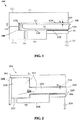
- FIG. 1 is a cross-sectional illustration of a conventional small volume chamber wafer processing system during a conventional small volume chamber etching process.
- System 100 has a rectangular cross-section that includes a grounded upper confinement chamber portion 102, a grounded lower confinement chamber portion 104, a removable floating confinement ring 108, an electro-static chuck (ESC) 106, a radio frequency (RF) driver 110 connected to ESC 106 and an exhaust portion 114.
- ESC electro-static chuck
- RF radio frequency
- Grounded upper confinement chamber portion 102 is able to be detachably disposed from grounded lower confinement chamber portion 104 at boundary 120, as indicated by the arrow.
- removable floating confinement ring 108 may be serviced or replaced, and further, a wafer may be disposed onto ESC 106 for processing.
- plasma sheath When a plasma is in contact with a negatively biased surface, such as an electrode or wall, a strong localized electric field appears between the plasma and that surface.
- This boundary layer called a "plasma sheath,” is a region of very low electron density, and serves as a medium to accelerate ions from the plasma to the electrode or wall surface. The energy that the ions gain as they are accelerated through plasma sheath regulates both the physical and chemical process at the surfaces surrounding the plasma.
- plasma sheath 118 of thickness t1 122 forms between plasma 116 and the surrounding solid surfaces exposed to plasma-forming space 112 (grounded upper confinement chamber portion 102, grounded lower confinement chamber portion 104, removable floating confinement ring 108, and ESC 106).
- the electrode area of ESC 106 is about the same as the electrode area of the grounded surfaces exposed to plasma-forming space 112 (grounded upper confinement chamber portion 102, grounded lower confinement chamber portion 104, and removable floating confinement ring 108).
- a wafer 124 is held on ESC 106 via an electrostatic force.
- a voltage differential is provided between ESC 106 and grounded portions (grounded upper confinement chamber portion 102, grounded lower confinement chamber portion 104, and removable floating confinement ring 108), via RF driver 110, while pressure is decreased in plasma-forming space 112.
- an etching material is supplied into plasma-forming space 112 via an etching material source (not shown).
- the pressure within plasma-forming space 112 and the voltage differential, as created by RF driver 110, is set such that the etching material supplied into plasma-forming space 112 creates plasma 116.
- Plasma 116 etches material within plasma-forming space 112, which includes wafer 124.
- plasma sheath 118 of thickness t1 122 extends between plasma 116 and a bottom surface 126 of grounded upper confinement chamber portion 102, an inner surface 128 of removable floating confinement ring 108, a top surface 130 of grounded lower confinement chamber portion 104, and ESC 106.
- plasma sheath 118 of thickness t1 122 extends between plasma 116 and a bottom surface 126 of grounded upper confinement chamber portion 102, an inner surface 128 of removable floating confinement ring 108, a top surface 130 of grounded lower confinement chamber portion 104, and ESC 106.
- ion energies are typically needed. Such extremely high ion energies can be achieved by increasing an applied RF voltage to ESC 106 as supplied by RF driver 110.
- the ion energies of plasma 116 are defined by the potential difference between wafer 124 and plasma 116.
- Wafer DC bias is related to the electrode area ratio between ESC 106 and grounded upper confinement chamber portion 102, removable floating confinement ring 108 and grounded lower confinement chamber portion 104.
- DC bias is also directly related to the difference between the potential of plasma 116 with respect to the grounded surfaces (grounded upper confinement chamber portion 102, removable floating confinement ring 108 and grounded lower confinement chamber portion 104) and the potential of plasma 116 with respect to wafer 124.
- the electrode area and the corresponding wafer DC bias will be discussed in more detail below.
- the combined electrode area of the powered electrode with respect to the combined electrode area of the grounded surfaces is conventionally referred to as the electrode area ratio.
- the electrode area ratio is a function of the areas of the physical surfaces and is also a function of the electrical properties of the materials of the physical surfaces.
- Using different materials for parts of system 100 may change the electrical properties thereof by changing the impedance between the ESC 106 and grounded upper confinement chamber portion 102, removable floating confinement ring 108 and grounded lower confinement chamber portion 104.
- removable floating confinement ring 108 may be removably disposed and replaced with a different confinement ring having different electrical properties and having it either electrically floating or grounded. Such a replacement may change the electrical properties of system 100 thus changing the area ratio and ultimately changing the DC bias between ESC 106 and grounded upper confinement chamber portion 102 and grounded lower confinement chamber portion 104.
- High aspect ratio (HAR) etching typically demands extremely high ion energies at the surface of wafer 124, and therefore may require increased driving voltages from RF driver 110, for increased periods of time. These increased driving voltages result in higher plasma potential within plasma-forming space 112 therefore resulting in higher energy ions bombarding the grounded surfaces (bottom surface 126 of grounded upper confinement chamber portion 102, inner surface 128 of removable floating confinement ring 108 and top surface 130 of grounded lower confinement chamber portion 104) as well as the surface of wafer 124.
- the plasma potential, and therefore t1 sheath potential may be adjusted by increasing the electrode area ratio between ESC 106 and the grounded portions, i.e., grounded upper confinement chamber portion 102 and grounded lower confinement chamber portion 104.
- the electrode area ratio may be increased by increasing at least one of the physical surface area or changing the electrical properties of at least one of grounded upper confinement chamber portion 102 and grounded lower confinement chamber portion 104.
- a conventional large volume chamber wafer processing system which will be discussed in more detail below, has an increased electrode area ratio over the conventional small volume chamber wafer processing system as discussed above.
- the conventional large volume chamber wafer processing system has a much larger plasma-forming space, which is bounded by grounded surfaces, as compared to the plasma-forming space of the conventional small volume chamber wafer processing system. Therefore, the conventional large volume chamber wafer processing system has a much larger grounded surface area as compared to the grounded surface area in the conventional small volume chamber wafer processing system.
- the conventional large volume chamber wafer processing system has an increased wafer DC bias as compared to the conventional small volume chamber wafer processing system.
- Large ground-to-powered electrode area ratio not only increases the ion energy at the wafer surface but decreases the plasma potential, and therefore decreases wear rate of grounded chamber parts that face plasma.
- FIG. 2 is a cross-sectional illustration of a conventional large volume chamber wafer processing system during a conventional large volume chamber etching process.
- System 200 includes a grounded upper confinement chamber portion 202, a grounded lower confinement chamber portion 204, a grounded chamber wall portion 208, an ESC 206, and an RF driver 210 connected to ESC 206.
- a plasma-forming space 212 is bounded by grounded upper confinement chamber portion 202, grounded lower confinement chamber portion 204, ESC 206 and grounded chamber wall portion 208.
- a wafer 220 is held onto ESC 206 via an electrostatic force.
- RF driver 210 provides an RF signal to ESC 206 to create plasma 224, similar to the manner discussed above, in plasma-forming space 212.
- Plasma sheath 218 of thickness t 2 226 exists between plasma 224 and grounded surfaces (grounded upper confinement chamber portion 202, grounded lower confinement chamber portion 204, and grounded chamber wall portion 208).
- a different plasma sheath (not shown) with a larger thickness exists between plasma 224 and wafer 220, since now the electrode area of the powered electrode (ESC 206 ) is different from the area of the grounded electrodes.
- This difference in the plasma sheaths allows for high-energy ions (corresponding to thicker plasma sheath and larger sheath potential) to be provided to the surface of wafer 220 while low-energy ions (corresponding to thinner plasma sheath and smaller sheath potential) to be provided to the grounded chamber portions.
- Plasma-forming space 212 includes a first plasma-forming space portion 216, which corresponds to plasma-forming space 112 as discussed above with reference to system 100 in FIG. 1 , in addition to plasma-forming space 214.
- system 200 has a larger grounded surface area as compared to the grounded surface area of system 100.
- grounded upper confinement chamber portion 102 of system 100; grounded lower confinement chamber portion 204 of system 200 has a larger surface area than grounded lower confinement chamber portion 104 of system 100; and grounded chamber wall portion 208 of system 200 has a larger surface area than removable floating confinement ring 108 of system 100.
- the increased surface area described above provides a larger area ratio between ESC 206 and grounded chamber portions, which in this case include grounded upper confinement chamber portion 202, grounded lower confinement chamber portion 204 and grounded chamber wall portion 208.
- this larger area ratio increases ion energy at wafer 220 while decreasing the potential of plasma 224 with respect to ground and decreasing the thickness t2 226 of plasma sheath 218.
- the potential of plasma sheath 218 is smaller than the potential of plasma sheath 118, and therefore results in lower ion energy provided to the grounded chamber portions, and thus resulting in lower wear rate.
- the difference between the potentials of sheath 218 and sheath 118 is related to the difference in the electrode area ratio of system 200 and the area ratio of system 100.
- system 200 is able to provide less plasma sheath potential (and therefore less ion energy) to its grounded chamber portions than system 100.
- the increased ion energy at wafer 220 increases the etch rate of system 200 over system 100. This is the benefit of a conventional large volume chamber as compared to a conventional small volume chamber.
- the conventional large volume chamber shown in FIG. 2 does not include a removable floating confinement ring. Therefore, unlike the conventional small volume chamber shown in FIG. 1 , the electrical properties of chamber of FIG. 2 may not be readily changed in order to adjust the area ratio and ultimately adjust and optimize the wafer DC bias.
- system 200 of FIG. 2 has an increase in wafer DC bias over the wafer DC bias of system 100, whereas system 200 has more expensive overall operation and less flexibility with no replaceable floating confinement ring.
- Document US-A1-2004/0159286 discloses a plasma treatment device wherein a baffle plate having an L-shaped or J-shaped cross-section is fitted between a ceiling and side wall of a vacuum chamber. The baffle plate confines the plasma into the upper portion of the chamber.
- Document US-A1-2008/0314522 discloses an apparatus configured to confine a plasma within a processing region in a plasma processing chamber by means of a confinement ring.
- the wafer processing system has an increased wafer DC bias over the conventional small volume chamber wafer processing system while providing less operating costs than the conventional large volume chamber wafer processing system.
- a small volume chamber wafer processing system includes a confinement ring that is shaped so as to have an increased surface area over those of conventional confinement rings. Accordingly, a confinement ring in accordance with the present invention will provide an increased area ratio between a powered electrode and grounded surfaces to provide an increased wafer DC bias. Therefore, a small volume chamber wafer processing system in accordance with the present invention provides increased wafer DC bias over the conventional small volume chamber wafer processing system while providing lower operating costs than the conventional large volume chamber wafer processing system.
- FIG. 3 An example small volume chamber wafer processing system in accordance with an aspect of the present invention, during a wafer processing process (etching), will now be described with reference to FIG. 3 .
- system 300 includes grounded upper confinement chamber portion 102, grounded lower confinement chamber portion 104, a removable C-shaped grounded confinement ring 308, ESC 106, RF driver 110 connected to ESC 106 and exhaust portion 114.
- a plasma-forming space 312 is bounded by top surface 132 of ESC 106, grounded bottom surface 126 of upper confinement chamber portion 102, top surface 130 of grounded lower confinement chamber portion 104 and inner surface 302 of removable C-shaped grounded confinement ring 308.
- a wafer 320 is held onto ESC 106 via an electrostatic force.
- RF driver 110 provides an RF signal to ESC 106 to create plasma 316, similar to the manner discussed above in reference to FIG. 1 , in plasma-forming space 312.
- Plasma sheath 318 of thickness t 3 326 exists between plasma 316 and grounded surfaces (grounded upper confinement chamber portion 102, grounded lower confinement chamber portion 104, and removable C-shaped grounded confinement ring 308 .)
- removable C-shaped grounded confinement ring 308 has a non-rectangular cross section as compared to the rectangular cross section of removable floating confinement ring 108, system 300 has a larger grounded surface area as compared to the grounded surface area of system 100.
- the increased grounded surface area in accordance with this aspect of the present invention provides a larger area ratio between ESC 106 and grounded chamber portions, which include grounded upper confinement chamber portion 102, grounded lower confinement chamber portion 104 and removable C-shaped grounded confinement ring 308 as compared to the conventional system discussed above with respect to FIG. 1 .
- This larger area ratio increases wafer DC bias and increases ion energy at wafer 320.
- the larger area ratio additionally provides less plasma potential to plasma 316 with respect to grounded upper confinement chamber portion 102, grounded lower confinement chamber portion 104 and removable C-shaped grounded confinement ring 308 as compared to the conventional system discussed above with respect to FIG. 1 .
- the decreased plasma potential thickness t3 326 of plasma sheath 318 is less than thickness t1 122 of plasma sheath 118 as provided by system 100 of FIG. 1 .
- the thickness of the resulting plasma sheath is decreased from thickness t1 122 to thickness t3 326 around grounded upper confinement chamber portion 102, grounded lower confinement chamber portion 104 and removable C-shaped grounded confinement ring 308.
- system 300 is operable to generate plasma 316 having greater wafer DC bias and less plasma potential with respect to its grounded chamber portions than system 100, but is operable to generate plasma 316 having less wafer DC bias and more plasma potential with respect to its grounded chamber portions than system 200.
- FIG. 4 is a graph having an x-axis representing a maximum ion energy, measured in electron-volts, at a wafer surface during an etching process and a y-axis representing a maximum plasma potential, measured in volts.
- a function 402 corresponds to measured results for system 100 using removable floating confinement ring 108.
- a function 404 corresponds to measured results for system 300 using a removable C-shaped grounded confinement ring 308 in accordance with an aspect of the present invention.
- system 300 using removable C-shaped grounded confinement ring 308 in accordance with an aspect of the present invention provides much higher maximum ion energy at the wafer for a given maximum plasma potential than that of system 100 using removable floating confinement ring 108.
- data point 406 on function 402 indicates that system 100 using removable floating confinement ring 108 provides a maximum plasma potential of approximately 1100 V for a maximum ion energy at the wafer of approximately 3400 eV (Electron Volts).
- data point 408 on function 404 indicates that system 300 using a removable C-shaped grounded confinement ring 308 in accordance with an aspect of the present invention provides a maximum plasma potential of approximately 1100 V for a maximum ion energy at the wafer of approximately 4600 eV.
- data point 410 on function 402 indicates that system 100 using removable floating confinement ring 108 provides a maximum plasma potential of approximately 1600 V for a maximum ion energy at the wafer of approximately 4200 eV.
- data point 412 on function 404 indicates that system 300 using a removable C-shaped grounded confinement ring 308 in accordance with an aspect of the present invention provides a maximum plasma potential of approximately 1600 V for a maximum ion energy at the wafer of approximately 5300 eV.
- system 300 using removable C-shaped grounded confinement ring 308 in accordance with an aspect of the present invention provides an approximate 30% increase in the maximum ion energy at the wafer as compared to system 100 using removable floating confinement ring 108.
- An increased ion energy at the wafer surface produces an increased etch rate.
- using removable C-shaped grounded confinement ring 308 in accordance with an aspect of the present invention provides increased etch rate as compared to system 100 using removable floating confinement ring 108.
- a removable C-shaped grounded confinement ring 308 in accordance with an aspect of the present invention will provide a decreased ion energy as compared to system 200, which does not include any confinement ring.
- system 300 has a similar volume chamber as that of system 100. Therefore system 300 has a much smaller surface area to be cleaned after each processed wafer, as compared to system 200. Accordingly, system 300 using a removable C-shaped grounded confinement ring 308 in accordance with an aspect of the present invention has a decreased cost of operation, i.e., decreased power, money, time and material to operate, as compared to system 200.
- C-shaped grounded confinement ring 308 may be replaced to modify the electrical properties of system 300.
- the electrical properties may therefore be readily modified in order to adjust the area ratio and ultimately adjust and optimize the wafer DC bias for specific applications.
- Removable C-shaped grounded confinement ring 308 may also be negatively affected over time (through use) but may be replaced at a fraction of the cost of replacing the entire chamber.
- system 200 does not have a removable confinement ring it does not have this flexibility to optimize the wafer DC bias of the chamber or be repaired/replaced due to wear. This will further reduce the cost of operation of system 300 as compared with the cost of operation of system 200.
- FIG. 5 Another example small volume chamber wafer processing system in accordance with an aspect of the present invention will now be described with reference to FIG. 5 .
- system 500 includes grounded upper confinement chamber portion 102, grounded lower confinement chamber portion 104, a removable C-shaped grounded confinement ring 308, ESC 106, RF driver 110 connected to ESC 106 and exhaust portion 114.
- System 500 additionally includes RF filter 502, RF filter 504 and RF filter 508.
- Each of RF filters 502, 504 and 508 may take the form of any known filter that is operable to control RF current to ground.
- a change in impedance will change ion energy at wafer 320 and will change the potential of plasma 516 with respect to ground.
- a change in impedance may change the thickness t4 526 of plasma sheath 518 as compared to the thickness t3 326 of plasma sheath 318. Being able to change the impedance of grounded chamber portions thus allows for adjustment of plasma shape and also ion energies.
- the grounded confinement ring is referred to as a "C-shaped" grounded confinement ring because the non-rectangular cross sectional shape resembles a "C".
- other embodiments of grounded confinement ring in accordance with an aspect of the present disclosure have a non-rectangular cross sectional shape that does not resemble a C, but still have an increased surface area as compared to a grounded confinement ring having a rectangular cross sectional shape. Additional example embodiments of non-rectangular grounded confinement rings will now be described below with reference to FIGs. 6-9 .
- FIG. 6 Another example small volume chamber wafer processing system in accordance with an aspect of the present invention, during a wafer processing process (etching), will now be described with reference to FIG. 6 .
- system 600 includes grounded upper confinement chamber portion 102, grounded lower confinement chamber portion 104, a removable protrusioned grounded confinement ring 608, ESC 106, RF filter 502, RF filter 504, RF filter 508, RF driver 110 connected to ESC 106 and exhaust portion 114.
- System 600 differs from system 500 discussed above with reference to FIG. 5 in that removable C-shaped grounded confinement ring 308 has been replaced with removable protrusioned grounded confinement ring 608.
- the inner surface of removable protrusioned grounded confinement ring 608 has a plurality of protrusions 602, which therefore provides a larger surface area as compared to C-shaped grounded confinement ring 308.
- Protrusions 602 may take any shape, a non-limiting example of which includes long thin spikes.
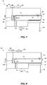
- FIG. 7 Another example small volume chamber wafer processing system in accordance with an aspect of the present invention, during a wafer processing process (etching), is illustrated in FIG. 7 .
- system 700 differs from system 600 discussed above with reference to FIG. 6 in that removable protrusioned grounded confinement ring 608 has been replaced with removable finned grounded confinement ring 708.
- the inner surface of removable finned grounded confinement ring 708 has a plurality of fins 702, which therefore provides a larger surface area as compared to C-shaped grounded confinement ring 308.
- system 800 differs from system 600 discussed above with reference to FIG. 6 in that removable protrusioned grounded confinement ring 608 has been replaced with removable spiked grounded confinement ring 808.
- the inner surface of removable spiked grounded confinement ring 808 has a plurality of spikes 802, which therefore provides a larger surface area as compared to C-shaped grounded confinement ring 308.
- system 900 differs from system 600 discussed above with reference to FIG. 6 in that removable protrusioned grounded confinement ring 608 has been replaced with removable grounded confinement ring 908 having a convex portion 902.
- the inner surface of removable grounded confinement ring 908 has convex portion 902, which therefore provides a larger surface area as compared to C-shaped grounded confinement ring 308.
- each of removable protrusioned grounded confinement ring 608 of FIG. 6 , removable finned grounded confinement ring 708 of FIG. 7 , removable spiked grounded confinement ring 808 of FIG. 8 and removable grounded confinement ring 908 having a convex portion 902 of FIG. 9 provides a larger surface area as compared to C-shaped grounded confinement ring 308 of FIG. 5 . Therefore, each of removable protrusioned grounded confinement ring 608, removable finned grounded confinement ring 708, removable spiked grounded confinement ring 808 and removable grounded confinement ring 908 has a larger total surface area of the grounded electrode as compared to system 500 of FIG. 5 .
- each of removable protrusioned grounded confinement ring 608, removable finned grounded confinement ring 708, removable spiked grounded confinement ring 808 and removable grounded confinement ring 908 is able to provide a larger wafer DC bias as compared to system 500 of FIG. 5 .
- the larger wafer DC bias leads to an increased ion energy at wafer 320 and a decreased potential of plasma with respect to grounded electrodes.
- a thickness t 5 626 of plasma sheath 618 of system 600, a thickness t 6 726 of plasma sheath 718 of system 700, a thickness t 7 826 of plasma sheath 818 of system 800 and a thickness t 8 926 of plasma sheath 918 of system 900 are each less than thickness t 4 526 of plasma sheath 518 of system 500.
- system 500, 600, 700, 800 and 900 The overall benefit of system 500, 600, 700, 800 and 900 is the increased area ratio due to the added physical area of a grounded confinement ring with a non-rectangular cross section.
- each of system 600, system 700, system 800 and system 900 may provide an increased ion energy at wafer 320 as compared with system 500, each of system 600, system 700, system 800 and system 900 may have an increased cost of operation due the increased area that needs to be auto-cleaned.
- polymer deposition on the surface of a grounded confinement ring can be controlled by heating up the grounded confinement ring elevated temperatures during etch processes.
- Each of thickness t 8 926, t 7 826 , t 6 726 and t 5 626 are less than the thickness t 4 526 of plasma sheath 518, which is less than thickness t 3 326 .
- Systems 500, 600, 700, 800 and 900 also maintain the benefit of a small volume chamber system that reduces the WAC process, thus saving time, energy and money while increasing the lifespan of grounded upper confinement chamber portion 102, grounded lower confinement chamber portion 104 and removable grounded confinement rings 308, 608, 708, 808 and 908.
- a small volume chamber wafer processing system has an increased wafer DC bias compared to conventional small volume chamber wafer processing system 100 and provides less operating costs than conventional large volume chamber wafer processing system 200.
Landscapes
- Physics & Mathematics (AREA)
- Engineering & Computer Science (AREA)
- Plasma & Fusion (AREA)
- Chemical & Material Sciences (AREA)
- Analytical Chemistry (AREA)
- Drying Of Semiconductors (AREA)
- Plasma Technology (AREA)
Claims (10)
- Waferbearbeitungssystem zur Verwendung mit einem Treiber und einer Materialversorgungsquelle, wobei der Treiber (110) dazu betreibbar ist, ein Treibersignal zu erzeugen, wobei die Materialversorgungsquelle dazu betreibbar ist, ein Material bereitzustellen, wobei das Waferbearbeitungssystem Folgendes umfasst:einen oberen Einschlusskammerabschnitt (102), der eine Innenfläche des oberen Einschlusskammerabschnitts (126, 526, 626, 726, 826, 926) aufweist;einen unteren Einschlusskammerabschnitt (104), der abnehmbar in Kontakt mit dem oberen Einschlusskammerabschnitt (102) angeordnet ist, wobei der untere Einschlusskammerabschnitt eine Innenfläche des unteren Einschlusskammerabschnitts (130) aufweist;einen Einschlussring (308, 608, 708, 808, 908), der entfernbar in Kontakt mit der Innenfläche des oberen Einschlusskammerabschnitts und der Innenfläche des unteren Einschlusskammerabschnitts angeordnet ist, wobei der Einschlussring eine Einschlussring-Innenfläche (302) aufweist; undeine elektrostatische Einspannvorrichtung (106), die eine Oberseite der elektrostatischen Einspannvorrichtung aufweist und dafür angeordnet ist, in Betrieb das Treibersignal zu empfangen,wobei der obere Einschlusskammerabschnitt (102), der untere Einschlusskammerabschnitt (104), der Einschlussring (308, 608, 708, 808, 908) und die elektrostatische Einspannvorrichtung derart angeordnet sind, dass die Unterseite des oberen Einschlusskammerabschnitts (126, 526, 626, 726, 826, 926), die Oberseite des unteren Einschlusskammerabschnitts (130), die Einschlussring-Innenfläche (302) und die Oberseite der elektrostatischen Einspannvorrichtung (132) einen plasmabildenden Raum (312) umgeben, der imstande ist, das Material aufzunehmen,wobei der obere Einschlusskammerabschnitt (102), der untere Einschlusskammerabschnitt (104), der Einschlussring (308, 608, 708, 808, 908) und die elektrostatische Einspannvorrichtung (106) dazu betreibbar sind, das Material in ein Plasma umzuwandeln, wenn die elektrostatische Einspannvorrichtung das Treibersignal empfängt, undwobei der Einschlussring einen nicht rechteckigen, c-förmigen Querschnitt aufweist.
- Waferbearbeitungssystem nach Anspruch 1, wobei die Innenfläche des Einschlussrings (608, 708, 808, 908) einen Vorsprung (602, 702, 802, 902) umfasst.
- Waferbearbeitungssystem nach Anspruch 2, wobei der Vorsprung eine Rippe umfasst.
- Waferbearbeitungssystem nach Anspruch 2, wobei der Vorsprung einen Dorn umfasst.
- Waferbearbeitungssystem nach Anspruch 2, wobei der Vorsprung einen Höcker umfasst.
- Einschlussring (308, 608, 708, 808, 908) zur Verwendung mit einem Waferbearbeitungssystem, das einen Treiber, eine Materialversorgungsquelle, einen oberen Einschlusskammerabschnitt (102), einen unteren Einschlusskammerabschnitt (104) und eine elektrostatische Einspannvorrichtung (106) beinhaltet, wobei der Treiber dazu betreibbar ist, ein Treibersignal zu erzeugen, wobei die Materialversorgungsquelle dazu betreibbar ist, ein Material bereitzustellen, wobei der obere Einschlusskammerabschnitt eine Innenfläche des oberen Einschlusskammerabschnitts (126, 526, 626, 726, 826, 926) aufweist, wobei der untere Einschlusskammerabschnitt (104) abnehmbar in Kontakt mit dem oberen Einschlusskammerabschnitt (102) angeordnet ist, wobei der untere Einschlusskammerabschnitt (104) eine Innenfläche des unteren Einschlusskammerabschnitts (130) aufweist, wobei die elektrostatische Einspannvorrichtung (106) eine Oberseite der elektrostatischen Einspannvorrichtung aufweist und dafür angeordnet ist, das Treibersignal zu empfangen, wobei der Einschlussring (308, 608, 708, 808, 908) Folgendes umfasst:eine erste Einschlussringoberfläche, die entfernbar in Kontakt mit der Innenfläche des oberen Einschlusskammerabschnitts angeordnet ist;eine zweite Einschlussringoberfläche, die entfernbar in Kontakt mit der Innenfläche des unteren Einschlusskammerabschnitts angeordnet ist; undeine Einschlussring-Innenfläche;wobei, wenn er mit dem Waferbearbeitungssystem verwendet wird, der Einschlussring derart angeordnet ist, dass die erste Einschlussringoberfläche entfernbar in Kontakt mit der Innenfläche des oberen Einschlusskammerabschnitts (126, 526, 626, 726, 826, 926) angeordnet ist und die zweite Einschlussringoberfläche entfernbar in Kontakt mit der Innenfläche des unteren Einschlusskammerabschnitts (130) angeordnet ist, wobei, wenn der Einschlussring mit dem Waferbearbeitungssystem verwendet wird, der obere Einschlusskammerabschnitt (102), der untere Einschlusskammerabschnitt (104), die Einschlussring-Innenfläche (302) und die elektrostatische Einspannvorrichtung (106) derart angeordnet sind, dass die Innenfläche des oberen Einschlusskammerabschnitts (126, 526, 626, 726, 826, 926), die Innenfläche des unteren Einschlusskammerabschnitts (130), die Einschlussring-Innenfläche (302) und die Oberseite der elektrostatischen Einspannvorrichtung einen plasmabildenden Raum umgeben, der imstande ist, das Material aufzunehmen, undwobei der Einschlussring der Einschlussring einen nicht rechteckigen, c-förmigen Querschnitt aufweist.
- Einschlussring (608, 708, 808, 908) nach Anspruch 6, wobei die Einschlussring-Innenfläche einen Vorsprung umfasst.
- Einschlussring (608, 708, 808, 908) nach Anspruch 7, wobei der Vorsprung eine Rippe umfasst.
- Einschlussring (608, 708, 808, 908) nach Anspruch 7, wobei der Vorsprung einen Dorn umfasst.
- Einschlussring (608, 708, 808, 908) nach Anspruch 7, wobei der Vorsprung einen Höcker umfasst.
Applications Claiming Priority (3)
| Application Number | Priority Date | Filing Date | Title |
|---|---|---|---|
| US16698009P | 2009-04-06 | 2009-04-06 | |
| US12/570,359 US9337004B2 (en) | 2009-04-06 | 2009-09-30 | Grounded confinement ring having large surface area |
| PCT/US2010/030021 WO2010117971A2 (en) | 2009-04-06 | 2010-04-06 | Grounded confinement ring having large surface area |
Publications (3)
| Publication Number | Publication Date |
|---|---|
| EP2417627A2 EP2417627A2 (de) | 2012-02-15 |
| EP2417627A4 EP2417627A4 (de) | 2015-09-23 |
| EP2417627B1 true EP2417627B1 (de) | 2018-08-15 |
Family
ID=42825211
Family Applications (1)
| Application Number | Title | Priority Date | Filing Date |
|---|---|---|---|
| EP10762276.3A Active EP2417627B1 (de) | 2009-04-06 | 2010-04-06 | Begrenzungsring und halbleiterwaferbearbeitungssystem damit |
Country Status (8)
| Country | Link |
|---|---|
| US (1) | US9337004B2 (de) |
| EP (1) | EP2417627B1 (de) |
| JP (1) | JP5629757B2 (de) |
| KR (1) | KR101727337B1 (de) |
| CN (1) | CN102379029B (de) |
| SG (2) | SG10201401259UA (de) |
| TW (1) | TWI524415B (de) |
| WO (1) | WO2010117971A2 (de) |
Families Citing this family (8)
| Publication number | Priority date | Publication date | Assignee | Title |
|---|---|---|---|---|
| KR102219924B1 (ko) * | 2009-08-31 | 2021-02-23 | 램 리써치 코포레이션 | 무선 주파수 (rf) 접지 복귀 장치들 |
| US20130122711A1 (en) * | 2011-11-10 | 2013-05-16 | Alexei Marakhtanov | System, method and apparatus for plasma sheath voltage control |
| US20140273538A1 (en) | 2013-03-15 | 2014-09-18 | Tokyo Electron Limited | Non-ambipolar electric pressure plasma uniformity control |
| CN106920724B (zh) * | 2015-12-24 | 2019-05-03 | 中微半导体设备(上海)股份有限公司 | 改善刻蚀对称性的等离子处理装置及调节方法 |
| KR102652014B1 (ko) * | 2020-05-12 | 2024-03-28 | 세메스 주식회사 | 기판 처리 장치 |
| CN114664622B (zh) * | 2020-12-23 | 2024-07-05 | 中微半导体设备(上海)股份有限公司 | 一种等离子体处理装置及调节方法 |
| CN114695063A (zh) * | 2022-03-16 | 2022-07-01 | 北京北方华创微电子装备有限公司 | 反应腔室及半导体工艺设备 |
| USD1109284S1 (en) | 2024-06-07 | 2026-01-13 | Asm Ip Holding B.V. | Flow control ring |
Family Cites Families (14)
| Publication number | Priority date | Publication date | Assignee | Title |
|---|---|---|---|---|
| US5641375A (en) * | 1994-08-15 | 1997-06-24 | Applied Materials, Inc. | Plasma etching reactor with surface protection means against erosion of walls |
| US6129808A (en) * | 1998-03-31 | 2000-10-10 | Lam Research Corporation | Low contamination high density plasma etch chambers and methods for making the same |
| US6178919B1 (en) * | 1998-12-28 | 2001-01-30 | Lam Research Corporation | Perforated plasma confinement ring in plasma reactors |
| US6863835B1 (en) * | 2000-04-25 | 2005-03-08 | James D. Carducci | Magnetic barrier for plasma in chamber exhaust |
| JP2002270598A (ja) * | 2001-03-13 | 2002-09-20 | Tokyo Electron Ltd | プラズマ処理装置 |
| US6842147B2 (en) | 2002-07-22 | 2005-01-11 | Lam Research Corporation | Method and apparatus for producing uniform processing rates |
| US7972467B2 (en) * | 2003-04-17 | 2011-07-05 | Applied Materials Inc. | Apparatus and method to confine plasma and reduce flow resistance in a plasma reactor |
| KR101001743B1 (ko) | 2003-11-17 | 2010-12-15 | 삼성전자주식회사 | 헬리컬 자기-공진 코일을 이용한 이온화 물리적 기상 증착장치 |
| CN1914714B (zh) * | 2004-03-31 | 2011-09-28 | 富士通半导体股份有限公司 | 基板处理装置及半导体装置的制造方法 |
| KR100790392B1 (ko) * | 2004-11-12 | 2008-01-02 | 삼성전자주식회사 | 반도체 제조장치 |
| US7837825B2 (en) * | 2005-06-13 | 2010-11-23 | Lam Research Corporation | Confined plasma with adjustable electrode area ratio |
| US8980049B2 (en) * | 2007-04-02 | 2015-03-17 | Charm Engineering Co., Ltd. | Apparatus for supporting substrate and plasma etching apparatus having the same |
| KR102219924B1 (ko) | 2009-08-31 | 2021-02-23 | 램 리써치 코포레이션 | 무선 주파수 (rf) 접지 복귀 장치들 |
| KR20120068847A (ko) | 2009-08-31 | 2012-06-27 | 램 리써치 코포레이션 | 플라즈마 한정을 실시하기 위한 다중 주변 링 장치 |
-
2009
- 2009-09-30 US US12/570,359 patent/US9337004B2/en active Active
-
2010
- 2010-04-06 KR KR1020117023459A patent/KR101727337B1/ko active Active
- 2010-04-06 JP JP2012504756A patent/JP5629757B2/ja active Active
- 2010-04-06 EP EP10762276.3A patent/EP2417627B1/de active Active
- 2010-04-06 WO PCT/US2010/030021 patent/WO2010117971A2/en not_active Ceased
- 2010-04-06 TW TW099110612A patent/TWI524415B/zh active
- 2010-04-06 SG SG10201401259UA patent/SG10201401259UA/en unknown
- 2010-04-06 SG SG2011068277A patent/SG174502A1/en unknown
- 2010-04-06 CN CN201080014577.8A patent/CN102379029B/zh active Active
Non-Patent Citations (1)
| Title |
|---|
| None * |
Also Published As
| Publication number | Publication date |
|---|---|
| CN102379029B (zh) | 2014-04-02 |
| JP5629757B2 (ja) | 2014-11-26 |
| TW201108325A (en) | 2011-03-01 |
| TWI524415B (zh) | 2016-03-01 |
| WO2010117971A3 (en) | 2011-01-13 |
| WO2010117971A2 (en) | 2010-10-14 |
| JP2012523135A (ja) | 2012-09-27 |
| KR20120014892A (ko) | 2012-02-20 |
| EP2417627A2 (de) | 2012-02-15 |
| CN102379029A (zh) | 2012-03-14 |
| US20100252200A1 (en) | 2010-10-07 |
| EP2417627A4 (de) | 2015-09-23 |
| US9337004B2 (en) | 2016-05-10 |
| SG174502A1 (en) | 2011-11-28 |
| KR101727337B1 (ko) | 2017-04-14 |
| SG10201401259UA (en) | 2014-05-29 |
Similar Documents
| Publication | Publication Date | Title |
|---|---|---|
| EP2417627B1 (de) | Begrenzungsring und halbleiterwaferbearbeitungssystem damit | |
| KR101654868B1 (ko) | 플라즈마 처리 장치, 플라즈마 처리 방법, 프로그램을 기록한 기록매체 | |
| US7837826B2 (en) | Hybrid RF capacitively and inductively coupled plasma source using multifrequency RF powers and methods of use thereof | |
| CN110462798B (zh) | 在感应耦合等离子体处理室内以低偏压产生近衬底补充等离子体密度 | |
| KR102631507B1 (ko) | 웨이퍼의 선단 에지에서의 피처 프로파일 틸팅을 개선하기 위한 에지 링 어셈블리 | |
| CN101653048B (zh) | Rf供电电极上的dc电压控制的方法和设备 | |
| US5605637A (en) | Adjustable dc bias control in a plasma reactor | |
| JP4838736B2 (ja) | プラズマ処理装置 | |
| JP5348848B2 (ja) | プラズマ処理装置 | |
| US8635971B2 (en) | Tunable uniformity in a plasma processing system | |
| KR101749766B1 (ko) | 플라즈마 처리 방법 및 플라즈마 처리 장치 | |
| US20120258555A1 (en) | Multi-Frequency Hollow Cathode and Systems Implementing the Same | |
| US9799491B2 (en) | Low electron temperature etch chamber with independent control over plasma density, radical composition and ion energy for atomic precision etching | |
| US20120255678A1 (en) | Multi-Frequency Hollow Cathode System for Substrate Plasma Processing | |
| KR20080044169A (ko) | 반경 방향 플라즈마 분포에 대한 개선된 자기 제어를 위한플라즈마 제한 배플 및 유동비 이퀄라이저 | |
| JP5305287B2 (ja) | 半導体製造装置 | |
| US20230238264A1 (en) | Multi-Zone Platen Temperature Control | |
| US10964514B2 (en) | Electrode for plasma processing chamber | |
| JP4873718B2 (ja) | プラズマ処理装置及びプラズマ処理方法 | |
| KR20050034190A (ko) | 멀티 캐패시터를 갖는 플라즈마 식각 장치 |
Legal Events
| Date | Code | Title | Description |
|---|---|---|---|
| PUAI | Public reference made under article 153(3) epc to a published international application that has entered the european phase |
Free format text: ORIGINAL CODE: 0009012 |
|
| 17P | Request for examination filed |
Effective date: 20111107 |
|
| AK | Designated contracting states |
Kind code of ref document: A2 Designated state(s): AT BE BG CH CY CZ DE DK EE ES FI FR GB GR HR HU IE IS IT LI LT LU LV MC MK MT NL NO PL PT RO SE SI SK SM TR |
|
| DAX | Request for extension of the european patent (deleted) | ||
| A4 | Supplementary search report drawn up and despatched |
Effective date: 20150825 |
|
| RIC1 | Information provided on ipc code assigned before grant |
Ipc: H01J 37/32 20060101ALI20150819BHEP Ipc: H01L 21/67 20060101ALI20150819BHEP Ipc: H01L 21/3065 20060101AFI20150819BHEP Ipc: H05H 1/24 20060101ALI20150819BHEP |
|
| GRAP | Despatch of communication of intention to grant a patent |
Free format text: ORIGINAL CODE: EPIDOSNIGR1 |
|
| STAA | Information on the status of an ep patent application or granted ep patent |
Free format text: STATUS: GRANT OF PATENT IS INTENDED |
|
| INTG | Intention to grant announced |
Effective date: 20180329 |
|
| RIC1 | Information provided on ipc code assigned before grant |
Ipc: H05H 1/24 20060101ALI20180320BHEP Ipc: H01L 21/67 20060101ALI20180320BHEP Ipc: H01L 21/3065 20060101AFI20180320BHEP Ipc: H01J 37/32 20060101ALI20180320BHEP |
|
| GRAS | Grant fee paid |
Free format text: ORIGINAL CODE: EPIDOSNIGR3 |
|
| GRAA | (expected) grant |
Free format text: ORIGINAL CODE: 0009210 |
|
| STAA | Information on the status of an ep patent application or granted ep patent |
Free format text: STATUS: THE PATENT HAS BEEN GRANTED |
|
| AK | Designated contracting states |
Kind code of ref document: B1 Designated state(s): AT BE BG CH CY CZ DE DK EE ES FI FR GB GR HR HU IE IS IT LI LT LU LV MC MK MT NL NO PL PT RO SE SI SK SM TR |
|
| REG | Reference to a national code |
Ref country code: CH Ref legal event code: EP Ref country code: GB Ref legal event code: FG4D Ref country code: AT Ref legal event code: REF Ref document number: 1030732 Country of ref document: AT Kind code of ref document: T Effective date: 20180815 |
|
| REG | Reference to a national code |
Ref country code: IE Ref legal event code: FG4D |
|
| REG | Reference to a national code |
Ref country code: DE Ref legal event code: R096 Ref document number: 602010052771 Country of ref document: DE |
|
| REG | Reference to a national code |
Ref country code: NL Ref legal event code: MP Effective date: 20180815 |
|
| REG | Reference to a national code |
Ref country code: LT Ref legal event code: MG4D |
|
| REG | Reference to a national code |
Ref country code: AT Ref legal event code: MK05 Ref document number: 1030732 Country of ref document: AT Kind code of ref document: T Effective date: 20180815 |
|
| PG25 | Lapsed in a contracting state [announced via postgrant information from national office to epo] |
Ref country code: NO Free format text: LAPSE BECAUSE OF FAILURE TO SUBMIT A TRANSLATION OF THE DESCRIPTION OR TO PAY THE FEE WITHIN THE PRESCRIBED TIME-LIMIT Effective date: 20181115 Ref country code: BG Free format text: LAPSE BECAUSE OF FAILURE TO SUBMIT A TRANSLATION OF THE DESCRIPTION OR TO PAY THE FEE WITHIN THE PRESCRIBED TIME-LIMIT Effective date: 20181115 Ref country code: SE Free format text: LAPSE BECAUSE OF FAILURE TO SUBMIT A TRANSLATION OF THE DESCRIPTION OR TO PAY THE FEE WITHIN THE PRESCRIBED TIME-LIMIT Effective date: 20180815 Ref country code: GR Free format text: LAPSE BECAUSE OF FAILURE TO SUBMIT A TRANSLATION OF THE DESCRIPTION OR TO PAY THE FEE WITHIN THE PRESCRIBED TIME-LIMIT Effective date: 20181116 Ref country code: NL Free format text: LAPSE BECAUSE OF FAILURE TO SUBMIT A TRANSLATION OF THE DESCRIPTION OR TO PAY THE FEE WITHIN THE PRESCRIBED TIME-LIMIT Effective date: 20180815 Ref country code: LT Free format text: LAPSE BECAUSE OF FAILURE TO SUBMIT A TRANSLATION OF THE DESCRIPTION OR TO PAY THE FEE WITHIN THE PRESCRIBED TIME-LIMIT Effective date: 20180815 Ref country code: FI Free format text: LAPSE BECAUSE OF FAILURE TO SUBMIT A TRANSLATION OF THE DESCRIPTION OR TO PAY THE FEE WITHIN THE PRESCRIBED TIME-LIMIT Effective date: 20180815 Ref country code: IS Free format text: LAPSE BECAUSE OF FAILURE TO SUBMIT A TRANSLATION OF THE DESCRIPTION OR TO PAY THE FEE WITHIN THE PRESCRIBED TIME-LIMIT Effective date: 20181215 Ref country code: AT Free format text: LAPSE BECAUSE OF FAILURE TO SUBMIT A TRANSLATION OF THE DESCRIPTION OR TO PAY THE FEE WITHIN THE PRESCRIBED TIME-LIMIT Effective date: 20180815 |
|
| PG25 | Lapsed in a contracting state [announced via postgrant information from national office to epo] |
Ref country code: LV Free format text: LAPSE BECAUSE OF FAILURE TO SUBMIT A TRANSLATION OF THE DESCRIPTION OR TO PAY THE FEE WITHIN THE PRESCRIBED TIME-LIMIT Effective date: 20180815 Ref country code: HR Free format text: LAPSE BECAUSE OF FAILURE TO SUBMIT A TRANSLATION OF THE DESCRIPTION OR TO PAY THE FEE WITHIN THE PRESCRIBED TIME-LIMIT Effective date: 20180815 Ref country code: ES Free format text: LAPSE BECAUSE OF FAILURE TO SUBMIT A TRANSLATION OF THE DESCRIPTION OR TO PAY THE FEE WITHIN THE PRESCRIBED TIME-LIMIT Effective date: 20180815 |
|
| PG25 | Lapsed in a contracting state [announced via postgrant information from national office to epo] |
Ref country code: CZ Free format text: LAPSE BECAUSE OF FAILURE TO SUBMIT A TRANSLATION OF THE DESCRIPTION OR TO PAY THE FEE WITHIN THE PRESCRIBED TIME-LIMIT Effective date: 20180815 Ref country code: IT Free format text: LAPSE BECAUSE OF FAILURE TO SUBMIT A TRANSLATION OF THE DESCRIPTION OR TO PAY THE FEE WITHIN THE PRESCRIBED TIME-LIMIT Effective date: 20180815 Ref country code: RO Free format text: LAPSE BECAUSE OF FAILURE TO SUBMIT A TRANSLATION OF THE DESCRIPTION OR TO PAY THE FEE WITHIN THE PRESCRIBED TIME-LIMIT Effective date: 20180815 Ref country code: EE Free format text: LAPSE BECAUSE OF FAILURE TO SUBMIT A TRANSLATION OF THE DESCRIPTION OR TO PAY THE FEE WITHIN THE PRESCRIBED TIME-LIMIT Effective date: 20180815 Ref country code: PL Free format text: LAPSE BECAUSE OF FAILURE TO SUBMIT A TRANSLATION OF THE DESCRIPTION OR TO PAY THE FEE WITHIN THE PRESCRIBED TIME-LIMIT Effective date: 20180815 |
|
| REG | Reference to a national code |
Ref country code: DE Ref legal event code: R097 Ref document number: 602010052771 Country of ref document: DE |
|
| PG25 | Lapsed in a contracting state [announced via postgrant information from national office to epo] |
Ref country code: SK Free format text: LAPSE BECAUSE OF FAILURE TO SUBMIT A TRANSLATION OF THE DESCRIPTION OR TO PAY THE FEE WITHIN THE PRESCRIBED TIME-LIMIT Effective date: 20180815 Ref country code: DK Free format text: LAPSE BECAUSE OF FAILURE TO SUBMIT A TRANSLATION OF THE DESCRIPTION OR TO PAY THE FEE WITHIN THE PRESCRIBED TIME-LIMIT Effective date: 20180815 Ref country code: SM Free format text: LAPSE BECAUSE OF FAILURE TO SUBMIT A TRANSLATION OF THE DESCRIPTION OR TO PAY THE FEE WITHIN THE PRESCRIBED TIME-LIMIT Effective date: 20180815 |
|
| PLBE | No opposition filed within time limit |
Free format text: ORIGINAL CODE: 0009261 |
|
| STAA | Information on the status of an ep patent application or granted ep patent |
Free format text: STATUS: NO OPPOSITION FILED WITHIN TIME LIMIT |
|
| 26N | No opposition filed |
Effective date: 20190516 |
|
| PG25 | Lapsed in a contracting state [announced via postgrant information from national office to epo] |
Ref country code: SI Free format text: LAPSE BECAUSE OF FAILURE TO SUBMIT A TRANSLATION OF THE DESCRIPTION OR TO PAY THE FEE WITHIN THE PRESCRIBED TIME-LIMIT Effective date: 20180815 |
|
| REG | Reference to a national code |
Ref country code: CH Ref legal event code: PL |
|
| REG | Reference to a national code |
Ref country code: BE Ref legal event code: MM Effective date: 20190430 |
|
| GBPC | Gb: european patent ceased through non-payment of renewal fee |
Effective date: 20190406 |
|
| PG25 | Lapsed in a contracting state [announced via postgrant information from national office to epo] |
Ref country code: MC Free format text: LAPSE BECAUSE OF FAILURE TO SUBMIT A TRANSLATION OF THE DESCRIPTION OR TO PAY THE FEE WITHIN THE PRESCRIBED TIME-LIMIT Effective date: 20180815 Ref country code: LU Free format text: LAPSE BECAUSE OF NON-PAYMENT OF DUE FEES Effective date: 20190406 |
|
| PG25 | Lapsed in a contracting state [announced via postgrant information from national office to epo] |
Ref country code: GB Free format text: LAPSE BECAUSE OF NON-PAYMENT OF DUE FEES Effective date: 20190406 Ref country code: CH Free format text: LAPSE BECAUSE OF NON-PAYMENT OF DUE FEES Effective date: 20190430 Ref country code: LI Free format text: LAPSE BECAUSE OF NON-PAYMENT OF DUE FEES Effective date: 20190430 |
|
| PG25 | Lapsed in a contracting state [announced via postgrant information from national office to epo] |
Ref country code: BE Free format text: LAPSE BECAUSE OF NON-PAYMENT OF DUE FEES Effective date: 20190430 Ref country code: FR Free format text: LAPSE BECAUSE OF NON-PAYMENT OF DUE FEES Effective date: 20190430 |
|
| PG25 | Lapsed in a contracting state [announced via postgrant information from national office to epo] |
Ref country code: TR Free format text: LAPSE BECAUSE OF FAILURE TO SUBMIT A TRANSLATION OF THE DESCRIPTION OR TO PAY THE FEE WITHIN THE PRESCRIBED TIME-LIMIT Effective date: 20180815 |
|
| PG25 | Lapsed in a contracting state [announced via postgrant information from national office to epo] |
Ref country code: IE Free format text: LAPSE BECAUSE OF NON-PAYMENT OF DUE FEES Effective date: 20190406 |
|
| PG25 | Lapsed in a contracting state [announced via postgrant information from national office to epo] |
Ref country code: PT Free format text: LAPSE BECAUSE OF FAILURE TO SUBMIT A TRANSLATION OF THE DESCRIPTION OR TO PAY THE FEE WITHIN THE PRESCRIBED TIME-LIMIT Effective date: 20181215 |
|
| PG25 | Lapsed in a contracting state [announced via postgrant information from national office to epo] |
Ref country code: CY Free format text: LAPSE BECAUSE OF FAILURE TO SUBMIT A TRANSLATION OF THE DESCRIPTION OR TO PAY THE FEE WITHIN THE PRESCRIBED TIME-LIMIT Effective date: 20180815 |
|
| PG25 | Lapsed in a contracting state [announced via postgrant information from national office to epo] |
Ref country code: MT Free format text: LAPSE BECAUSE OF FAILURE TO SUBMIT A TRANSLATION OF THE DESCRIPTION OR TO PAY THE FEE WITHIN THE PRESCRIBED TIME-LIMIT Effective date: 20180815 Ref country code: HU Free format text: LAPSE BECAUSE OF FAILURE TO SUBMIT A TRANSLATION OF THE DESCRIPTION OR TO PAY THE FEE WITHIN THE PRESCRIBED TIME-LIMIT; INVALID AB INITIO Effective date: 20100406 |
|
| PG25 | Lapsed in a contracting state [announced via postgrant information from national office to epo] |
Ref country code: MK Free format text: LAPSE BECAUSE OF FAILURE TO SUBMIT A TRANSLATION OF THE DESCRIPTION OR TO PAY THE FEE WITHIN THE PRESCRIBED TIME-LIMIT Effective date: 20180815 |
|
| P01 | Opt-out of the competence of the unified patent court (upc) registered |
Effective date: 20231021 |
|
| PGFP | Annual fee paid to national office [announced via postgrant information from national office to epo] |
Ref country code: DE Payment date: 20250429 Year of fee payment: 16 |
|
| REG | Reference to a national code |
Ref country code: DE Ref legal event code: R079 Ref document number: 602010052771 Country of ref document: DE Free format text: PREVIOUS MAIN CLASS: H01L0021306500 Ipc: H10P0050240000 |