EP2415166B1 - Breitband-störer-detektor - Google Patents
Breitband-störer-detektor Download PDFInfo
- Publication number
- EP2415166B1 EP2415166B1 EP10712260.8A EP10712260A EP2415166B1 EP 2415166 B1 EP2415166 B1 EP 2415166B1 EP 10712260 A EP10712260 A EP 10712260A EP 2415166 B1 EP2415166 B1 EP 2415166B1
- Authority
- EP
- European Patent Office
- Prior art keywords
- transistor
- coupled
- terminal
- signal
- circuit
- Prior art date
- Legal status (The legal status is an assumption and is not a legal conclusion. Google has not performed a legal analysis and makes no representation as to the accuracy of the status listed.)
- Not-in-force
Links
- 238000001514 detection method Methods 0.000 claims description 55
- 239000003990 capacitor Substances 0.000 claims description 32
- 238000010586 diagram Methods 0.000 description 13
- 238000000034 method Methods 0.000 description 13
- 238000004891 communication Methods 0.000 description 10
- 230000007704 transition Effects 0.000 description 10
- 230000008569 process Effects 0.000 description 8
- 230000010355 oscillation Effects 0.000 description 6
- 238000010168 coupling process Methods 0.000 description 4
- 238000005859 coupling reaction Methods 0.000 description 4
- 230000006870 function Effects 0.000 description 4
- 230000008878 coupling Effects 0.000 description 3
- 238000013461 design Methods 0.000 description 3
- 238000005516 engineering process Methods 0.000 description 3
- 230000003287 optical effect Effects 0.000 description 3
- 238000005070 sampling Methods 0.000 description 3
- 230000035945 sensitivity Effects 0.000 description 3
- 238000012935 Averaging Methods 0.000 description 2
- 239000000835 fiber Substances 0.000 description 2
- 239000002245 particle Substances 0.000 description 2
- 239000008186 active pharmaceutical agent Substances 0.000 description 1
- 230000003321 amplification Effects 0.000 description 1
- 230000008859 change Effects 0.000 description 1
- 239000002800 charge carrier Substances 0.000 description 1
- 238000004590 computer program Methods 0.000 description 1
- 230000000593 degrading effect Effects 0.000 description 1
- 230000001419 dependent effect Effects 0.000 description 1
- 230000009977 dual effect Effects 0.000 description 1
- 230000000694 effects Effects 0.000 description 1
- 230000007274 generation of a signal involved in cell-cell signaling Effects 0.000 description 1
- 238000005259 measurement Methods 0.000 description 1
- 238000010295 mobile communication Methods 0.000 description 1
- 238000012986 modification Methods 0.000 description 1
- 230000004048 modification Effects 0.000 description 1
- 238000003199 nucleic acid amplification method Methods 0.000 description 1
- 238000012546 transfer Methods 0.000 description 1
- 230000001960 triggered effect Effects 0.000 description 1
Images


Classifications
-
- H—ELECTRICITY
- H03—ELECTRONIC CIRCUITRY
- H03F—AMPLIFIERS
- H03F1/00—Details of amplifiers with only discharge tubes, only semiconductor devices or only unspecified devices as amplifying elements
- H03F1/08—Modifications of amplifiers to reduce detrimental influences of internal impedances of amplifying elements
- H03F1/083—Modifications of amplifiers to reduce detrimental influences of internal impedances of amplifying elements in transistor amplifiers
- H03F1/086—Modifications of amplifiers to reduce detrimental influences of internal impedances of amplifying elements in transistor amplifiers with FET's
-
- H—ELECTRICITY
- H03—ELECTRONIC CIRCUITRY
- H03F—AMPLIFIERS
- H03F1/00—Details of amplifiers with only discharge tubes, only semiconductor devices or only unspecified devices as amplifying elements
- H03F1/08—Modifications of amplifiers to reduce detrimental influences of internal impedances of amplifying elements
-
- G—PHYSICS
- G05—CONTROLLING; REGULATING
- G05F—SYSTEMS FOR REGULATING ELECTRIC OR MAGNETIC VARIABLES
- G05F3/00—Non-retroactive systems for regulating electric variables by using an uncontrolled element, or an uncontrolled combination of elements, such element or such combination having self-regulating properties
- G05F3/02—Regulating voltage or current
- G05F3/08—Regulating voltage or current wherein the variable is DC
- G05F3/10—Regulating voltage or current wherein the variable is DC using uncontrolled devices with non-linear characteristics
- G05F3/16—Regulating voltage or current wherein the variable is DC using uncontrolled devices with non-linear characteristics being semiconductor devices
- G05F3/20—Regulating voltage or current wherein the variable is DC using uncontrolled devices with non-linear characteristics being semiconductor devices using diode- transistor combinations
- G05F3/26—Current mirrors
-
- H—ELECTRICITY
- H03—ELECTRONIC CIRCUITRY
- H03F—AMPLIFIERS
- H03F1/00—Details of amplifiers with only discharge tubes, only semiconductor devices or only unspecified devices as amplifying elements
- H03F1/42—Modifications of amplifiers to extend the bandwidth
- H03F1/48—Modifications of amplifiers to extend the bandwidth of aperiodic amplifiers
- H03F1/483—Modifications of amplifiers to extend the bandwidth of aperiodic amplifiers with field-effect transistors
-
- H—ELECTRICITY
- H04—ELECTRIC COMMUNICATION TECHNIQUE
- H04B—TRANSMISSION
- H04B1/00—Details of transmission systems, not covered by a single one of groups H04B3/00 - H04B13/00; Details of transmission systems not characterised by the medium used for transmission
- H04B1/06—Receivers
- H04B1/10—Means associated with receiver for limiting or suppressing noise or interference
- H04B1/1027—Means associated with receiver for limiting or suppressing noise or interference assessing signal quality or detecting noise/interference for the received signal
-
- H—ELECTRICITY
- H04—ELECTRIC COMMUNICATION TECHNIQUE
- H04B—TRANSMISSION
- H04B1/00—Details of transmission systems, not covered by a single one of groups H04B3/00 - H04B13/00; Details of transmission systems not characterised by the medium used for transmission
- H04B1/69—Spread spectrum techniques
- H04B1/707—Spread spectrum techniques using direct sequence modulation
- H04B1/7097—Interference-related aspects
Definitions
- the present disclosure relates generally to electronics, and more specifically to a wideband jammer detector.
- Communication devices such as Code Division Multiple Access (CDMA) Global System for Mobile communications (GSM) and Wireless Local Area Network (WLAN) communication devices
- CDMA Code Division Multiple Access
- GSM Global System for Mobile communications
- WLAN Wireless Local Area Network
- Communication devices include receiver circuits, which utilize correlation circuits to decipher a desired communication signal from all other received signals. Device performance is degraded when jammer signals are present during the correlation process.
- Jammer signals can be introduced by internal or external sources.
- An internal jammer signal is a jammer signal which is introduced by the receiver.
- An example is a clock spur generated by a voltage controlled oscillator (VCO) within the receiver.
- VCO voltage controlled oscillator
- An external jammer signal is a jammer signal, which is introduced by a source external to the receiver.
- An example is a signal transmitted by a transmitter in another communication device that generates out-of-band emissions in the receive frequency band of the receiver.
- a jammer signal impacts the sensitivity of a receiver in two ways. It can for example de-sense an analog-to-digital converter in the receiver thereby degrading its sensitivity.
- a jammer signal that appears at odd harmonics of a local oscillator signal in the receiver is down converted into the receive band to degrade signal sensitivity at baseband. Thus, errors may be introduced into the demodulated data packet when jammer signals are not detected by the receiver.
- a jammer detector detects close in jammer signals, such as jammer signals close to the receive (RX) band.
- RX receive
- a wideband jammer detector is capable of also detecting jammer signals hundreds of MHz away from the RX band.
- a jammer detector allows the receiver to operate in an un-protected or low power mode when no jammer signal is present and in protected or high power mode in the presence of jammer signals.
- a digital high frequency power detection circuit includes a peak detecting circuit and a peak computing circuit.
- the peak detecting circuit is operably coupled to detect a peak value of a high frequency signal and includes an amplifier, transistor, and capacitor.
- the amplifier has a 1 st input, 2 nd input and an output, where the 1 st input is operably coupled to receive the high frequency signal.
- the transistor has a gate, a drain, and a source, where the gate is coupled to the output of the amplifier, the source is coupled to a supply voltage, and the drain is coupled to the 2 nd input of the amplified.
- the capacitor is operably coupled to the drain of the transistor and to a reference potential. The voltage imposed across the capacitor represents the peak value of the high frequency signal.;
- the peak computing circuit is operably coupled to generate a digital peak value from the peak value.
- the inductor peaking circuit has inductors and resistors inserted in series between the output part and a power supply, and capacitances coupled in parallel between the output part and an earth (GND), and depending on respective values of these inductors, resistors and capacitances, it is possible to suppress a peaking generated in the output part.
- high-speed current mirror resistive compensation circuits and output impedance boosting circuits are utilized to increase amplifier bandwidth in an improved wideband amplifier circuit.
- a dual transistor configuration including common source topology, averaging capacitors and a comparator circuit is utilized to improve the sensing of signal peaks in a peak detector block.
- the peak detector block is used together with the wideband amplifier circuit and a digital jammer detection circuit to detect jammer signals.
- the wideband amplifier circuit is used together with the peak detection circuit, a comparator circuit and a digital jammer detection circuit form a wideband jammer detector to detect jammer signals in a received signal of a communication device.
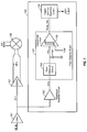
- a radio frequency input signal RF IN is amplified by a first low noise amplifier (LNA) 101 to generate amplified signal RF1.
- Amplified signal RF 1 is coupled at an input to the wideband jammer detector 100 and also to an input of a second low noise amplifier 107.
- a differential output signal RF3 is generated by the second low noise amplifier 107 to in-phase and quadrature (I/Q) mixer 108.
- Wideband jammer detector 100 comprises wideband amplifier circuit 102, peak detection circuit 103, averaging capacitor 104, comparator circuit 105, and digital jammer detection circuit 106.
- Wideband amplifier circuit 102 is a low power, wide bandwidth amplifier.
- Wideband amplifier circuit receives and amplifies RF1 from LNA 101 to generate amplified signal RF2.
- RF2 is connected to an input of peak detection circuit 103.
- Peak detection circuit 103 generates an output voltage level proportional to a peak voltage of amplified signal RF2.
- Capacitor 104 is coupled at one end to ground. The opposite end of capacitor 104 is coupled to the output of peak detection circuit 103 and to a sampling input Vin of comparator circuit 105. Capacitor 104 serves to average the output of peak detection circuit 103. Comparator circuit 105 also receives a reference input Vref. The output of comparator circuit 105 varies as a function of input signals Vin and Vref. When Vin is greater than or equal to Vref, the output PEAK_DET of comparator circuit 105 switches to a logic high state. Conversely, when Vin is less than Vref, the output PEAK_DET switches to a logic low state. Peak detection circuit 103, capacitor 104 and comparator circuit 105 define a peak detector block 107.
- PEAK_DET is coupled to the input of digital jammer detection circuit 106.
- Digital jammer detection circuit 106 samples the value of PEAK_DET over a programmed duration. The programmed duration may be controlled and varied during device operation. When digital jammer detection circuit 106 counts a programmed threshold number of logic level high samples within the programmed duration, digital jammer detection circuit 106 generates an interrupt output jammer detector signal JDET.
- FIG. 2A and 2B are circuit level diagrams of a standard current mirror circuit 200A and a high-speed current mirror resistive compensation circuit 200B, respectively.
- a standard current mirror circuit 200A as shown in FIG. 2A comprises a current source 201 and two transistors 202 and 203.
- Transistors 202 and 203 are NMOS devices.
- Transistor 202 is configured as the reference transistor with the drain of transistor 202 coupled to the gates of both transistors 202 and 203.
- a high-speed current mirror resistive compensation circuit as shown in FIG. 2B comprises a current source 204, resistor 205, and two NMOS transistors 206 and 207.
- a first terminal of resistor 205 is coupled to the gate of transistor 206.
- a second terminal of resistor 205 is coupled to the gate of transistor 207 and the drain of transistor 206.
- Transistor 206 is configured as the reference transistor with the drain of transistor 206 coupled to the gate of transistor 207 and to the second terminal of resistor 205.
- resistor 205 increases the theoretical 3dB cutoff frequency by a factor of 2 when resistor 205 has a resistive value equal to the reciprocal of the transconductance of transistor 206. This results in a significant increase in bandwidth.
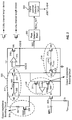
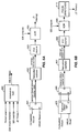
- FIG. 3 is a schematic diagram of a wideband amplifier circuit 300, a peak detector block 350, and a digital jammer detection circuit 360 in accordance with an exemplary embodiment.
- W ideband amplifier circuit 300 comprises capacitor C1, resistor R1, PMOS input transistor 302, first and second high-speed current mirror resistive compensation circuits 317, 318, operational amplifier 315, NMOS transistor 316, and first and second output impedance boosting circuits 319, 320.
- Peak detection block 350 may comprise peak detection circuit 103, capacitor 104 and comparator circuit 105, as in the standard receiver shown in FIG. 1 .
- digital jammer detection circuit may comprise a circuit as in the digital jammer detection circuit 106 in the standard receiver shown in FIG. 1 .
- peak detection block 350 and digital jammer detection circuit 360 may correspond to new digital logic circuits described below in connection with FIGs . 4 and 6 , respectively.
- high-speed current mirror resistive compensation circuit 317 includes resistor 305 and PMOS transistors 303 and 304.
- High-speed current mirror resistive compensation circuit 318 includes resistor 314 and NMOS transistors 312 and 313.
- a first terminal of capacitor C1 is coupled to the signal input RF1.
- a second terminal of capacitor C1 is coupled to the gate of transistor 302.
- the series coupling of the input signal RF1 through capacitor C1 provides AC-coupling of the input signal RF1.
- the AC coupling capacitor C1 isolates the DC level of the previous stage and allows NMOS transistor 302 to be biased at a desired value Vbias.
- a first terminal of resistor R1 is coupled to a voltage source V bias .
- a second terminal of resistor 301 is coupled to the gate of transistor 302. Varying V bias controls the bias voltage applied to the gate of transistor 302. When additional gain is desired Vbias is increased to create an increased voltage between the gate and the source, V GS , of transistor 302.
- ⁇ n the charge-carrier effective mobility
- W the gate width
- L the gate length
- C ox the gate oxide capacitance per unit area of transistor 302.
- the source of transistor 302 is coupled to ground.
- the drain of transistor 302 is coupled to an active load including high-speed current mirror resistive compensation circuit 317 and output impedance boosting circuit 319.
- high-speed current mirror resistive compensation circuit 317 provides additional bandwidth by introducing a zero.
- the output impedance boosting circuit 319 increases the output resistance of transistor 302. The increase in output resistance increases the gain provided by transistor 302.
- Output impedance boosting circuit 319 has two purposes. First, the output impedance boosting circuit diverts the DC current away from transistor 303, thereby allowing transistor 303 to be a small low current device with high bandwidth. Transistors 304 and 303 have a device size ratio of 4:1. The DC current as well as the RF current is amplified going from transistors 303 to 304. Second, output impedance boosting circuit 319 diverts the DC current away from the main path. However, output impedance boosting circuit 319 should not divert the RF signal from the main path. This is achieved by boosting the output impedance.
- the output of high-speed current mirror resistive compensation circuit 317 is coupled to high-speed current mirror resistive compensation circuit 318 and output impedance boosting circuit 320. Similar to output impedance boosting circuit 319, output impedance boosting circuit 320 has the same two purposes.
- the output impedance boosting is achieved with a different technique.
- the output of high-speed current mirror resistive compensation circuit 318 is coupled to the drain of transistor 316 and the negative input of operational amplifier 315.
- the positive input of operational amplifier 315 is coupled to a voltage source set to VDD/2.
- the operational amplifier 315 configuration drives the DC output of the wideband amplifier to VDD/2 by way of the virtual short effect between the inputs of an operational amplifier (OP AMP) 315.
- OP AMP 315 controls the gate voltage of transistor 316 to create a current source to feed transistor 313.
- OP AMP 315 ensures that the node RF2 is biased at VDD/2. This is achieved by driving the gate of the transistor M6 to whatever voltage in order that RF2 is set at VDD/2.
- RF2 feeds peak detector block 350.
- Gain DC g m M 1 W 4 ⁇ W 5 W 2 ⁇ W 3 R OUT
- a gain may be (i) equal to one in linear unit, which is zero dB in logarithm unit, (ii) greater than one in linear unit, or (iii) less than one in linear unit.
- a gain of greater than one in linear unit corresponds to signal amplification and a positive gain (in dB).
- a gain of less than one in linear unit corresponds to signal attenuation and a negative gain (in dB). Attenuation is negative gain, so that an attenuation of x dB is equivalent to a gain of - x dB.
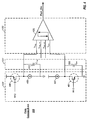
- FIG. 4 shows a schematic diagram of a peak detector block 350 in accordance with a further exemplary embodiment which can be used to peak detect the output RF2 from wideband amplifier circuit 102 in the standard receiver of FIG. 1 as well as a receiver incorporating the wideband amplifier circuit 300 shown in FIG. 3 .
- Peak detector block 350 includes a peak detection circuit 103', a capacitor coupling circuit 104' and a comparator circuit 105'.
- Peak detection circuit 103' includes an upper negative-peak detector portion and a lower positive-peak detector portion.
- the RF2 amplified output from a preceding stage is coupled to respective peak detector input transistors 400 and 401 in each of upper negative-peak and lower positive-peak detector portions.
- Transistor 400 is a PMOS transistor.
- the source of transistor 400 is coupled to VDD.
- PMOS transistor 400 is biased in weak inversion region to allow it to follow the negative peak of an amplified jammer signal.
- the drain of transistor 400 is coupled to current source 406.
- PMOS transistor 400 is configured in a common source configuration to allow detection of negative peak signals.
- a first terminal of capacitor 402 is coupled to the drain of transistor 400 and the negative sampling input V neg of comparator 405.
- a second terminal of capacitor 402 is coupled to ground.
- Capacitor 402 averages the output of transistor 400 to create signal V neg .
- the negative threshold input V neg_ref is set to a selected threshold voltage level. In some designs the selected threshold voltage level V pos_ref may be programmable.
- Transistor 401 is a NMOS transistor biased to operate in the weak inversion region so the transistor will follow the positive peak of the amplified jammer signal.
- the source of transistor 401 is coupled to ground.
- the drain of transistor 401 is coupled to current source 407.
- NMOS transistor 401 is configured in a common source configuration to allow detection of positive peak signals.
- a first terminal of capacitor 403 is coupled to the drain of transistor 401 and the positive sampling input of comparator 405.
- a second terminal of capacitor 403 is coupled to ground.
- Capacitor 403 averages the output of transistor 401 to create signal V pos .
- the positive threshold input value V pos_ref is set to a selected threshold voltage level. In some designs, the selected threshold voltage level V pos_ref may be programmable.
- Transistors 400 and 401 are biased to operate in weak inversion mode, otherwise known as "Cut-off” or "Sub-threshold” mode.
- Weak inversion occurs when the gate to source voltage is less than the threshold voltage of the transistor.
- current should not flow through a transistor in weak inversion mode.
- some more energetic electrons at the source can enter the channel and flow to the drain of the transistor. This results in a sub-threshold current that is exponentially related to the gate to source voltage applied to the transistor. Operation in weak inversion mode allows transistors 400 and 401 to create an output current large enough to properly drive comparator 405.
- I D I DO e V GS ⁇ V th nV T
- C D capacitance of the depletion layer
- C OX capacitance of the oxide layer.
- Comparator 405 compares the amplitude of input signal V neg with the amplitude of threshold signal V neg_ref. Comparator 405 also compares the amplitude of input signal V pos with the amplitude of threshold signal V pos_ref . When either input signal has larger amplitude than the amplitude of the corresponding threshold signal, the comparator 405 output signal PEAK_DET is set to a logic high state. When both input signals have lower amplitude than the amplitude of the corresponding threshold signal the comparator 405 output signal PEAK_DET is set to a logic low state.
- a conventional digital jammer detection circuit 106 samples the output of comparator 105 over a programmed duration.
- the programmed duration may be controlled and varied during device operation.
- digital detection circuit 106 counts more than a programmed threshold number of logic level high samples within the programmed duration, digital detection circuit 106 generates an interrupt output signal JDET.
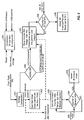
- FIG. 5 shows an operational flow diagram of a digital jammer detection circuit 360.
- the comparator circuit 150 and all counters are initialized. Step 500 may be initiated by different events, such as: powering on the device, jammer detection circuit timeout, single wire bus interface (SBI) override, global reset, or gain mode transition.
- a digital jammer detection circuit clock is reset.
- the first independent process includes steps 503, 504, and 505.
- the second independent process includes steps 506, 507, 508 and 509.
- the first independent process includes steps 503, 504, and 505.
- the digital jammer detection circuit timeout period is provided.
- the digital jammer detection circuit determines whether the jammer detection circuit timeout period provided in step 503 has elapsed. If the digital jammer detection circuit timeout period has not elapsed step 504 is repeated.
- a reset request is sent if the jammer timeout period has elapsed.
- the second independent process includes steps 506, 507, 508 and 509.
- step 506 the digital jammer detection circuit samples the output of comparator 105 and determines if the sampled output is a logic high signal. If the sampled output is not a logic high signal the counting is stopped and current count value is maintained. In step 507, the slave counter determines the average time the jammer was present. In step 508, the digital jammer detection circuit determines if the peak counter value is greater than the programmed peak threshold value. In step 509, a jammer interrupt signal is sent and a reset request generated sending the process back to step 501.
- the digital jammer detection circuit determines if an external reset request has been made.
- An external interrupt may be initiated by different events, such as: single wire bus interface (SBI) overwrite, global device reset, or gain mode transition.
- FIGs . 6A and 6B show two different digital logic configurations for implementing digital jammer detection circuit 360.
- Block 600 is the initialization logic, which generates a digital jammer detection circuit reset signal when any of the following inputs are triggered: global reset, gain mode transition, SBI override, or digital jammer detection circuit timeout.
- block 601 is an SR latch circuit.
- An SR latch circuit is an arrangement of logic gates that maintains a stable output after the inputs have been turned off.
- a SR latch circuit has a set input (S) and a reset input (R). When the set input is logic high state the output is set to a logic high state. When the reset input is a logic high state the output is set to a logic low state.
- the output of block 601 is coupled to the input of block 602.
- Block 602 is a relaxation oscillation circuit.
- a relaxation oscillation circuit is an oscillator circuit that utilizes a capacitor, which is charged gradually and then discharged rapidly.
- a relation circuit may be implemented with a resistor or current source, a capacitor, and a threshold device such as an injunction transistor or Gunn diode.
- the output of block 601 is ON the relaxation oscillator 602 creates an output signal, which oscillates at a predetermined frequency.
- the oscillating output signal is the digital jammer detection circuit clock.
- the relaxation oscillator output is coupled to the input of the 8-bit counter 603.
- the 8-bit counter 603 counts the oscillations sampled.
- 8-bit counter 603 outputs the number of oscillations, which have been observed.
- a first input to XOR circuit 604 is coupled to the output of the 8-bit counter 603.
- a second input of XOR circuit 604 is coupled to a SBI compare signal.
- XOR circuit 604 determines a threshold compare value from the SBI compare signal.
- XOR circuit 604 compares the number provided by the 8-bit counter 603 with the SBI compare value. If the number provided by the 8-bit counter 603 is greater than the SBI compare value the XOR circuit 604 generates a jammer detected interrupt signal.
- block 605 is a transition detect logic.
- Transition detect logic 605 detects any change or transition of the logic level of the input signals and generates a constantly high logic level on its corresponding output.
- the Q output of transition detect logic 605 is coupled to the S input of SR latch 606.
- the Q' output (inverse of Q output) of transition detect logic 605 is coupled to the R input of SR latch 606.
- the transition detector purpose is to detect the comparator output going high when a jammer signal is first present after the circuit is initialized. This starts the "scanning" mode when the circuit starts scanning for jammer signals.
- the transition detector triggers the timeout counter, which determines the time for which the circuit needs to scan for a jammer signal. If the jammer count reaches the desired threshold (determined by slave counter) before the timeout counter triggers then the JDET signal goes HIGH indicating jammer signal detection.
- Block 606 is an SR latch circuit.
- An SR latch circuit is an arrangement of logic gates that maintains a stable output after the inputs have been turned off.
- An SR latch circuit has a set input (S) and a reset input (R). When the set input is logic high state the output is set to a logic high state. When the reset input is a logic high state the output is set to a logic low state.
- the output of block 606 is coupled to the input of block 607.
- Block 607 is a relaxation oscillator.
- a relaxation oscillator is an oscillator circuit that utilizes a capacitor, which is charged gradually and then discharged rapidly.
- a relaxation oscillator may be implemented with a resistor or current source, a capacitor, and a threshold device such as a uni-junction transistor or Gunn diode.
- the output of block 606 is a logic high signal the relaxation oscillator 607 creates an output signal which oscillates at a predetermined frequency.
- the oscillating output signal is the digital jammer detection circuit clock.
- the relaxation oscillator output is coupled to the input of the 8-bit counter 608.
- the 8-bit counter 608 counts the oscillations sampled.
- 8-bit counter 608 outputs the number of oscillations, which have been observed.
- a first input to XOR circuit 609 is coupled to the output of 8-bit counter circuit 608.
- a second input of XOR circuit 609 is coupled to a SBI compare signal.
- XOR circuit 609 determines a threshold compare value from the SBI compare signal.
- XOR circuit 609 compares the number provided by the 8-bit counter 608 with the SBI compare value. If the number provided by the 8-bit counter 608 is greater than the SBI compare value the XOR circuit 609 generates a jammer detected interrupt signal.
- the output of XOR circuit 609 is coupled to the input of pulse stretcher circuit 610. Pulse stretcher 610 generates a extended reset signal, which is meant to reset the internal states/counters when a jammer timeout occurs
- FIG. 7 shows a block diagram of a receiver path.
- the differential output terminals of LNA 701 are coupled to I/Q mixer 702.
- the input signal coupled to the input of LNA 701 contains the desired RF signal, local oscillator (LO) signals, close in jammer signals and far out jammer signals.
- LO local oscillator
- wideband jammer detector 100 detects the presence of LO signals, close in jammer signals and far out jammer signals.
- DSP Digital Signal Processor
- ASIC Application Specific Integrated Circuit
- FPGA Field Programmable Gate Array
- a general purpose processor may be a microprocessor, but in the alternative, the processor may be any conventional processor, controller, microcontroller, or state machine.
- a processor may also be implemented as a combination of computing devices, e.g., a combination of a DSP and a microprocessor, a plurality of microprocessors, one or more microprocessors in conjunction with a DSP core, or any other such configuration.
- a software module may reside in Random Access Memory (RAM), flash memory, Read Only Memory (ROM), Electrically Programmable ROM (EPROM), Electrically Erasable Programmable ROM (EEPROM), registers, hard disk, a removable disk, a CD-ROM, or any other form of storage medium known in the art.
- An exemplary storage medium is coupled to the processor such that the processor can read information from, and write information to, the storage medium.
- the storage medium may be integral to the processor.
- the processor and the storage medium may reside in an ASIC.
- the ASIC may reside in a user terminal.
- the processor and the storage medium may reside as discrete components in a user terminal.
- the functions described may be implemented in hardware, software, firmware, or any combination thereof. If implemented in software, the functions may be stored on or transmitted over as one or more instructions or code on a computer-readable medium.
- Computer-readable media includes both computer storage media and communication media including any medium that facilitates transfer of a computer program from one place to another.
- a storage media may be any available media that can be accessed by a computer.
- such computer-readable media can comprise RAM, ROM, EEPROM, CD-ROM or other optical disk storage, magnetic disk storage or other magnetic storage devices, or any other medium that can be used to carry or store desired program code in the form of instructions or data structures and that can be accessed by a computer.
- any connection is properly termed a computer-readable medium.
- the software is transmitted from a website, server, or other remote source using a coaxial cable, fiber optic cable, twisted pair, digital subscriber line (DSL), or wireless technologies such as infrared, radio, and microwave
- the coaxial cable, fiber optic cable, twisted pair, DSL, or wireless technologies such as infrared, radio, and microwave are included in the definition of medium.
- Disk and disc includes compact disc (CD), laser disc, optical disc, digital versatile disc (DVD), floppy disk and blu-ray disc where disks usually reproduce data magnetically, while discs reproduce data optically with lasers. Combinations of the above should also be included within the scope of computer-readable media.
Landscapes
- Engineering & Computer Science (AREA)
- Power Engineering (AREA)
- Physics & Mathematics (AREA)
- General Physics & Mathematics (AREA)
- Nonlinear Science (AREA)
- Electromagnetism (AREA)
- Microelectronics & Electronic Packaging (AREA)
- Radar, Positioning & Navigation (AREA)
- Automation & Control Theory (AREA)
- Computer Networks & Wireless Communication (AREA)
- Signal Processing (AREA)
- Amplifiers (AREA)
- Noise Elimination (AREA)
Claims (13)
- Ein Spitzen- bzw. Spitzenwertdetektorblock (350), der einen ersten Transistor (400), einen zweiten Transistor (401), einen ersten Kondensator (402), einen zweiten Kondensator (403) und eine Vergleicher- bzw. Komparatorschaltung (105') aufweist, wobei:ein Gatter- bzw. Gate-Anschluss des ersten Transistors (400) an einen Signaleingang gekoppelt ist;ein Quellen- bzw. Source-Anschluss des ersten Transistors (400) an eine erste Leistungsquelle gekoppelt ist;ein Senken- bzw. Drain-Anschluss des ersten Transistors (400) an einen ersten Anschluss des ersten Kondensators und einen ersten Eingangsanschluss der Komparatorschaltung gekoppelt ist;ein zweiter Anschluss des ersten Kondensators (402) an einen Masseanschluss bzw. eine Massequelle gekoppelt ist;ein Gate-Anschluss des zweiten Transistors (401) an den Signaleingang gekoppelt ist;ein Source-Anschluss des zweiten Transistors (401) an den Masseanschluss bzw. die Massequelle gekoppelt ist;ein Drain-Anschluss des zweiten Transistors (401) an einen ersten Anschluss des zweiten Kondensators (403) und einen zweiten Eingangsanschluss der Komparatorschaltung gekoppelt ist, wobei die Komparatorschaltung (105') konfiguriert ist zum Vergleichen eines ersten Signals, das an den ersten Eingangsanschluss des Komparators vorgesehen wird, mit einem ersten Schwellenwertsignal, und zum Vergleichen eines zweiten Signals, das an den zweiten Eingangsanschluss des Komparators geliefert wird, mit einem zweiten Schwellenwertsignal; undein zweiter Anschluss des zweiten Kondensators (403) an den Masseanschluss bzw. die Massequelle gekoppelt ist.
- Spitzenwertdetektorblock (350) nach Anspruch 1, wobei der erste Transistor und/oder der zweite Transistor (400, 401) unter Vorspannung stehen, so dass sie in einem schwachen Inversionsmodus arbeiten.
- Spitzenwertdetektorblock (350) nach Anspruch 1, wobei der erste Transistor (400) ein PMOS-Transistor ist und der zweite Transistor (401) ein NMOS-Transistor ist.
- Spitzenwertdetektorblock (350) nach Anspruch 1, wobei die ersten und zweiten Transistoren (400, 401) in einer gemeinsamen Source-Konfiguration gekoppelt sind.
- Spitzenwertdetektorblock nach Anspruch 1, wobei jedes der ersten und zweiten Schwellenwertsignale programmierbar ist.
- Spitzenwertdetektorblock nach Anspruch 1, wobei der Drain-Anschluss des ersten Transistors an eine Stromquelle gekoppelt ist.
- Spitzenwertdetektorblock nach Anspruch 6, wobei der Drain-Anschluss des zweiten Transistors an eine zweite Stromquelle gekoppelt ist.
- Spitzenwertdetektorblock nach Anspruch 1, wobei die Komparatorschaltung konfiguriert ist zum Erzeugen eines Ausgangssignals mit einem ersten Wert ansprechend darauf, dass das erste Signal eine größere Amplitude hat als eine Amplitude des ersten Schwellenwertsignals, und wobei die Komparatorschaltung konfiguriert ist zum Erzeugen des Ausgangssignals mit dem ersten Wert ansprechend darauf, dass das zweite Signal, das an den zweiten Eingangsanschluss des Komparators vorgesehen wird, eine größere Amplitude hat als eine Amplitude des zweiten Schwellenwertsignals.
- Ein Breitband-Jammer- bzw. -Störer-Detektor (100), der Folgendes beinhaltet:eine Breitbandverstärkerschaltung (300),den Spitzenwertdetektorblock (350) nach Anspruch 1,eine Digital-Störer-Detektionsschaltung (360);wobei ein Signaleingang an einen Eingangsanschluss der Breitbandverstärkerschaltung (300) gekoppelt ist;ein Ausgansanschluss der Breitbandverstärkerschaltung an einen Eingangsanschluss des Spitzenwertdetektorblockes (350) gekoppelt ist;ein Ausgangsanschluss der Spitzenwertdetektionsschaltung (103) an einen ersten Eingangsanschluss der Komparatorschaltung (105) gekoppelt ist;ein Schwellenwertsignal an einen zweiten Eingangsanschluss der Komparatorschaltung (105) gekoppelt ist;ein Ausgang des Spitzenwertdetektorblockes (350) an einen Eingangsanschluss der Digital-Störer-Detektionsschaltung (360) gekoppelt ist; unddie Breitbandverstärkerschaltung (300) ein erste aktive Last und eine zweite aktive Last beinhaltet, wobei die erste aktive Last an einen Drain-Anschluss des Eingangs-Transistors (302) gekoppelt ist, wobei die erste aktive Last als eine Hochgeschwindigkeitsstromspiegelwiderstandskompensationsschaltung (318) konfiguriert ist, wobei die zweite aktive Last an den Drain-Anschluss des Eingangstransistors (302) gekoppelt ist, wobei die zweite aktive Last als eine Ausgangsimpedanzsteigerungsschaltung (320) konfiguriert ist.
- Breitband-Störer-Detektor (100) nach Anspruch 9, wobei das zweite Schwellenwertsignal ein programmierbares Schwellenwertsignal ist.
- Breitband-Störer-Detektor (100) nach Anspruch 9, wobei die Breitbandverstärkerschaltung weiter eine dritte aktive Last beinhaltet, die an einen Ausgang der ersten, aktiven Last gekoppelt ist, die als eine zweite Hochgeschwindigkeitsstromspiegelwiderstandskompensationsschaltung konfiguriert ist und eine vierte aktive Last an den Ausgang der ersten aktiven Last gekoppelt ist und als eine zweite Ausgangsimpedanzsteigerungsschaltung konfiguriert ist.
- Breitband-Störer-Detektor (100) nach Anspruch 9, wobei die Hochgeschwindigkeitsstromspiegelwiderstandskompensationsschaltung (318) Folgendes beinhaltet:einen ersten Transistor (312);einen zweiten Transistor (313); undeinen ersten Widerstand (314);wobei ein Drain-Anschluss des ersten Transistors an den Drain-Anschluss des Eingangstransistors gekoppelt ist;ein Source-Anschluss des ersten Transistors an einen Gate-Anschluss des zweiten Transistors gekoppelt ist;ein erster Anschluss des ersten Widerstands an den Gate-Anschluss des ersten Transistors gekoppelt ist;ein zweiter Anschluss des ersten Widerstands an einen Gate-Anschluss des zweiten Transistors gekoppelt ist;ein Source-Anschluss des ersten Transistors an eine Leistungsquelle gekoppelt ist; undein Source-Anschluss des zweiten Transistors an die Leistungsquelle gekoppelt ist.
- Breitband-Störer-Detektor (100) nach Anspruch 9, wobei die Digital-Störer-Detektionsschaltung (360) Folgendes aufweist:Mittel zum Verstärken eines empfangenen Signals;Mittel zum Messen eines Spitzenwertes des empfangenen Signals;Mittel zum Vergleichen des Spitzenwertes des empfangenen Signals mit einem Schwellenwertsignal;Mittle zum Zählen der Anzahl von Spitzenwerten, die vom Betrag her größer sind als das Schwellenwertsignal während einer erwünschten Dauer; undMittel zum Erzeugen eines Interrupt- bzw. Unterbrechungssignals, wenn eine gezählte Anzahl von Spitzenwerten größer ist als ein Schwellenwert.
Applications Claiming Priority (3)
| Application Number | Priority Date | Filing Date | Title |
|---|---|---|---|
| US16509009P | 2009-03-31 | 2009-03-31 | |
| US12/582,090 US8838017B2 (en) | 2009-03-31 | 2009-10-20 | Wideband jammer detector |
| PCT/US2010/029517 WO2010120562A2 (en) | 2009-03-31 | 2010-03-31 | Wideband jammer detector |
Publications (2)
| Publication Number | Publication Date |
|---|---|
| EP2415166A2 EP2415166A2 (de) | 2012-02-08 |
| EP2415166B1 true EP2415166B1 (de) | 2016-05-18 |
Family
ID=42783486
Family Applications (1)
| Application Number | Title | Priority Date | Filing Date |
|---|---|---|---|
| EP10712260.8A Not-in-force EP2415166B1 (de) | 2009-03-31 | 2010-03-31 | Breitband-störer-detektor |
Country Status (7)
| Country | Link |
|---|---|
| US (1) | US8838017B2 (de) |
| EP (1) | EP2415166B1 (de) |
| JP (1) | JP5502989B2 (de) |
| KR (3) | KR101367882B1 (de) |
| CN (2) | CN102369663B (de) |
| TW (1) | TW201126896A (de) |
| WO (1) | WO2010120562A2 (de) |
Families Citing this family (8)
| Publication number | Priority date | Publication date | Assignee | Title |
|---|---|---|---|---|
| US8744336B2 (en) * | 2008-08-27 | 2014-06-03 | Qualcomm Incorporated | Interference detection apparatus and method |
| US8988156B2 (en) * | 2013-03-15 | 2015-03-24 | Microchip Technology Incorporated | Low EMI wide frequency range oscillator with automatic digital amplitude control |
| US9531497B2 (en) * | 2013-05-29 | 2016-12-27 | Drexel University | Real-time and protocol-aware reactive jamming in wireless networks |
| GB2539465B (en) * | 2015-06-17 | 2022-02-09 | Kathrein Se | A method and system for producing a jammer signal |
| US10079644B2 (en) * | 2015-08-10 | 2018-09-18 | Finisar Corporation | Out-of-band signal detection |
| KR102175951B1 (ko) | 2019-01-07 | 2020-11-09 | 한국전자통신연구원 | 광대역 펄스 탐지기 및 그것의 동작 방법 |
| TWI780004B (zh) | 2022-02-17 | 2022-10-01 | 瑞昱半導體股份有限公司 | 訊號偵測電路以及訊號偵測方法 |
| CN114859111B (zh) * | 2022-05-09 | 2025-07-29 | 河南翔宇医疗设备股份有限公司 | 一种自动电平跟踪电路、方法、装置及介质 |
Family Cites Families (33)
| Publication number | Priority date | Publication date | Assignee | Title |
|---|---|---|---|---|
| US3958083A (en) * | 1974-02-26 | 1976-05-18 | Fujitsu Ltd. | Acquisition system for the SDMA/TDMA satellite communication system |
| US4752939A (en) * | 1986-09-03 | 1988-06-21 | Hughes Aircraft Company | Hidden preamble for frequency hopped synchronization |
| US4973966A (en) * | 1988-05-23 | 1990-11-27 | Abraham Zeewy | Apparatus for determining the speed of motion of slowly moving objects |
| CA2016641C (en) * | 1989-05-12 | 1995-07-11 | Toshiyuki Tanoi | Adaptive interframe prediction coded video communications system |
| US5471509A (en) * | 1993-03-18 | 1995-11-28 | Trw Inc. | Universal matched filter |
| US5448598A (en) * | 1993-07-06 | 1995-09-05 | Standard Microsystems Corporation | Analog PLL clock recovery circuit and a LAN transceiver employing the same |
| JPH08307924A (ja) | 1995-04-28 | 1996-11-22 | Kokusai Electric Co Ltd | 移動体通信の端末装置及びその制御方法 |
| JP3579241B2 (ja) | 1998-02-24 | 2004-10-20 | 三洋電機株式会社 | Fmラジオ受信機 |
| JP3415431B2 (ja) | 1998-03-20 | 2003-06-09 | 株式会社東芝 | 無線送受信機とその受信高周波ユニット及び制御ユニット |
| JP2001053630A (ja) | 1999-08-17 | 2001-02-23 | Hitachi Kokusai Electric Inc | 雑音抑圧機能を有する受信機 |
| US6429696B1 (en) * | 2000-02-08 | 2002-08-06 | Cheng-Yung Kao | Peak hold and calibration circuit |
| EP1302045A2 (de) * | 2000-07-21 | 2003-04-16 | PMC-Sierra Ltd. | Verringerung des verhältnisses von spitzenleistung zu mittleren leistung |
| US6980786B1 (en) * | 2001-01-16 | 2005-12-27 | Sequoia Communications Corp. | Adaptive receiver system that adjusts to the level of interfering signals |
| JP4130098B2 (ja) | 2001-06-13 | 2008-08-06 | サンヨー・オートメディア・センディリアン・バハド | 車載用fmチューナの妨害検出・判定回路及び自動チューニングプログラム |
| US7809087B2 (en) * | 2002-04-26 | 2010-10-05 | Qualcomm, Incorporated | Power detection techniques and discrete gain state selection for wireless networking |
| US6999735B2 (en) * | 2002-07-23 | 2006-02-14 | Broadcom Corp. | Digital high frequency power detection circuit |
| US7009603B2 (en) * | 2002-09-27 | 2006-03-07 | Tdk Semiconductor, Corp. | Method and apparatus for driving light emitting polymer displays |
| JP4094985B2 (ja) | 2003-04-28 | 2008-06-04 | 京セラ株式会社 | 信号強度測定装置およびそれを利用した受信装置 |
| US8270927B2 (en) * | 2004-03-29 | 2012-09-18 | Qualcom, Incorporated | Adaptive interference filtering |
| US7283851B2 (en) * | 2004-04-05 | 2007-10-16 | Qualcomm Incorporated | Power saving mode for receiver circuit blocks based on transmitter activity |
| KR100617787B1 (ko) * | 2004-06-29 | 2006-08-28 | 삼성전자주식회사 | 고속 퓨리에 변환을 이용하여 방해전파를 검출하는전세계위치확인 시스템 수신기 및 방법 |
| DK1635240T3 (da) | 2004-09-14 | 2010-06-07 | Dialog Semiconductor Gmbh | Dynamiske transkonduktansboostingteknikker til strømspejle |
| US7454190B2 (en) * | 2004-10-28 | 2008-11-18 | Infineon Technologies Ag | Receiver circuit for a receiving element |
| US7348808B2 (en) * | 2005-04-27 | 2008-03-25 | Pmc-Sierra, Inc. | Method and apparatus for detection of high-speed electrical signals |
| JP4808247B2 (ja) * | 2006-03-27 | 2011-11-02 | 富士通株式会社 | ピーキング制御回路 |
| US8014462B2 (en) * | 2006-03-28 | 2011-09-06 | Teledyne Licensing, Llc | Apparatus for performing alternating quadratures differential binary phase shift keying modulation and demodulation |
| US7660569B2 (en) * | 2006-04-04 | 2010-02-09 | Qualcomm Incorporated | Methods and apparatus for digital jammer detection |
| US8521198B2 (en) | 2006-05-12 | 2013-08-27 | Qualcomm, Incorporated | Dynamic LNA switch points based on channel conditions |
| US7843834B2 (en) * | 2006-09-15 | 2010-11-30 | Itron, Inc. | Use of minimal propagation delay path to optimize a mesh network |
| JP4294721B2 (ja) | 2006-12-08 | 2009-07-15 | パナソニック株式会社 | 映像信号出力回路およびこれを有する半導体集積回路 |
| US8862081B2 (en) * | 2007-01-19 | 2014-10-14 | Wi-Lan, Inc. | Transceiver with receive path performance diversity and combiner with jammer detect feedback |
| US7778051B2 (en) * | 2007-03-14 | 2010-08-17 | System General Corp. | Output current control circuit for power converter with a changeable switching frequency |
| US8744336B2 (en) * | 2008-08-27 | 2014-06-03 | Qualcomm Incorporated | Interference detection apparatus and method |
-
2009
- 2009-10-20 US US12/582,090 patent/US8838017B2/en active Active
-
2010
- 2010-03-31 EP EP10712260.8A patent/EP2415166B1/de not_active Not-in-force
- 2010-03-31 TW TW099110001A patent/TW201126896A/zh unknown
- 2010-03-31 KR KR1020117025753A patent/KR101367882B1/ko not_active Expired - Fee Related
- 2010-03-31 WO PCT/US2010/029517 patent/WO2010120562A2/en not_active Ceased
- 2010-03-31 CN CN201080014674.7A patent/CN102369663B/zh not_active Expired - Fee Related
- 2010-03-31 KR KR1020137010281A patent/KR101381311B1/ko not_active Expired - Fee Related
- 2010-03-31 JP JP2012503680A patent/JP5502989B2/ja not_active Expired - Fee Related
- 2010-03-31 CN CN201410003435.1A patent/CN103746659B/zh not_active Expired - Fee Related
- 2010-03-31 KR KR1020137010280A patent/KR101392376B1/ko not_active Expired - Fee Related
Also Published As
| Publication number | Publication date |
|---|---|
| KR101381311B1 (ko) | 2014-04-04 |
| CN103746659B (zh) | 2017-04-12 |
| WO2010120562A3 (en) | 2010-12-23 |
| CN102369663B (zh) | 2015-08-26 |
| CN103746659A (zh) | 2014-04-23 |
| US8838017B2 (en) | 2014-09-16 |
| CN102369663A (zh) | 2012-03-07 |
| JP5502989B2 (ja) | 2014-05-28 |
| US20100245151A1 (en) | 2010-09-30 |
| KR101392376B1 (ko) | 2014-05-08 |
| KR101367882B1 (ko) | 2014-02-26 |
| KR20130052657A (ko) | 2013-05-22 |
| KR20130052656A (ko) | 2013-05-22 |
| WO2010120562A2 (en) | 2010-10-21 |
| KR20120018304A (ko) | 2012-03-02 |
| TW201126896A (en) | 2011-08-01 |
| JP2012523173A (ja) | 2012-09-27 |
| EP2415166A2 (de) | 2012-02-08 |
Similar Documents
| Publication | Publication Date | Title |
|---|---|---|
| EP2415166B1 (de) | Breitband-störer-detektor | |
| US8310277B2 (en) | High linear fast peak detector | |
| US8446994B2 (en) | Gain control in a communication channel | |
| EP2534755B1 (de) | Breitband-lna mit rauschunterdrückung | |
| KR20020059355A (ko) | 무선 주파수 디바이스 및 이를 구비한 무선 주파수 수신기및 캐패시턴스 충전 방법 | |
| JP3971368B2 (ja) | 信号強度検波回路およびそれを用いた増幅率制御システム。 | |
| US6750715B2 (en) | Logarithmic IF amplifier with dynamic large signal bias circuit | |
| CN101803186A (zh) | 具有可调整尺寸的本机振荡器缓冲器及混频器 | |
| US7619472B1 (en) | Noise-shaped blocker-reject amplifier | |
| KR100462467B1 (ko) | 자동이득제어의 가변이득증폭회로 | |
| US7855604B1 (en) | Protection circuit and method for RF power amplifiers in WLAN transceivers | |
| Mittal et al. | Detecting continuous jamming attack using ultra-low power RSSI circuit | |
| JP5074279B2 (ja) | 信号処理装置 | |
| WO2024186407A1 (en) | Kickback reduction in bootstrapped switches | |
| US11994548B2 (en) | RF peak detector circuit | |
| EP2477337A1 (de) | Abschwächungssteuerungsvorrichtung, signalabschwächungsvorrichtung, automatische verstärkungssteuerungsvorrichtung, abschwächungssteuerungsverfahren und automatisches verstärkungssteuerungsverfahren | |
| Wu et al. | A high-speed single-photon detection scheme based on frequency domain filtering | |
| Ciobanu et al. | PADI-2,-3 and-4: The second iteration of the fast Preamplifier—Discriminator ASIC for time-of-flight measurements at CBM | |
| Fang | Mitigating MOSFET noise: analysis and implementation of chopper amplifiers for reduced flicker noise | |
| KR101867449B1 (ko) | 개선된 선형성을 갖는 금속 산화물 반도체(mos) | |
| Park et al. | A CMOS RF power detector using an improved unbalanced source coupled pair | |
| Singh et al. | A 70.8 MW wideband CMOS low-noise amplifier for WiMAX application | |
| JP2005079991A (ja) | 無線受信回路およびそれを備えた無線装置 | |
| JP2003008362A (ja) | 前置増幅回路およびその出力制御方法ならびに通信装置 |
Legal Events
| Date | Code | Title | Description |
|---|---|---|---|
| PUAI | Public reference made under article 153(3) epc to a published international application that has entered the european phase |
Free format text: ORIGINAL CODE: 0009012 |
|
| 17P | Request for examination filed |
Effective date: 20111031 |
|
| AK | Designated contracting states |
Kind code of ref document: A2 Designated state(s): AT BE BG CH CY CZ DE DK EE ES FI FR GB GR HR HU IE IS IT LI LT LU LV MC MK MT NL NO PL PT RO SE SI SK SM TR |
|
| DAX | Request for extension of the european patent (deleted) | ||
| 17Q | First examination report despatched |
Effective date: 20150324 |
|
| GRAP | Despatch of communication of intention to grant a patent |
Free format text: ORIGINAL CODE: EPIDOSNIGR1 |
|
| INTG | Intention to grant announced |
Effective date: 20151203 |
|
| RIN1 | Information on inventor provided before grant (corrected) |
Inventor name: SEN, SHREYAS Inventor name: MUTHALI, HARISH, S. |
|
| GRAS | Grant fee paid |
Free format text: ORIGINAL CODE: EPIDOSNIGR3 |
|
| GRAA | (expected) grant |
Free format text: ORIGINAL CODE: 0009210 |
|
| AK | Designated contracting states |
Kind code of ref document: B1 Designated state(s): AT BE BG CH CY CZ DE DK EE ES FI FR GB GR HR HU IE IS IT LI LT LU LV MC MK MT NL NO PL PT RO SE SI SK SM TR |
|
| REG | Reference to a national code |
Ref country code: GB Ref legal event code: FG4D |
|
| REG | Reference to a national code |
Ref country code: CH Ref legal event code: EP |
|
| REG | Reference to a national code |
Ref country code: IE Ref legal event code: FG4D Ref country code: AT Ref legal event code: REF Ref document number: 801229 Country of ref document: AT Kind code of ref document: T Effective date: 20160615 |
|
| REG | Reference to a national code |
Ref country code: DE Ref legal event code: R096 Ref document number: 602010033455 Country of ref document: DE |
|
| REG | Reference to a national code |
Ref country code: NL Ref legal event code: MP Effective date: 20160518 |
|
| REG | Reference to a national code |
Ref country code: LT Ref legal event code: MG4D |
|
| PG25 | Lapsed in a contracting state [announced via postgrant information from national office to epo] |
Ref country code: NL Free format text: LAPSE BECAUSE OF FAILURE TO SUBMIT A TRANSLATION OF THE DESCRIPTION OR TO PAY THE FEE WITHIN THE PRESCRIBED TIME-LIMIT Effective date: 20160518 Ref country code: FI Free format text: LAPSE BECAUSE OF FAILURE TO SUBMIT A TRANSLATION OF THE DESCRIPTION OR TO PAY THE FEE WITHIN THE PRESCRIBED TIME-LIMIT Effective date: 20160518 Ref country code: LT Free format text: LAPSE BECAUSE OF FAILURE TO SUBMIT A TRANSLATION OF THE DESCRIPTION OR TO PAY THE FEE WITHIN THE PRESCRIBED TIME-LIMIT Effective date: 20160518 Ref country code: NO Free format text: LAPSE BECAUSE OF FAILURE TO SUBMIT A TRANSLATION OF THE DESCRIPTION OR TO PAY THE FEE WITHIN THE PRESCRIBED TIME-LIMIT Effective date: 20160818 |
|
| REG | Reference to a national code |
Ref country code: AT Ref legal event code: MK05 Ref document number: 801229 Country of ref document: AT Kind code of ref document: T Effective date: 20160518 |
|
| PG25 | Lapsed in a contracting state [announced via postgrant information from national office to epo] |
Ref country code: ES Free format text: LAPSE BECAUSE OF FAILURE TO SUBMIT A TRANSLATION OF THE DESCRIPTION OR TO PAY THE FEE WITHIN THE PRESCRIBED TIME-LIMIT Effective date: 20160518 Ref country code: GR Free format text: LAPSE BECAUSE OF FAILURE TO SUBMIT A TRANSLATION OF THE DESCRIPTION OR TO PAY THE FEE WITHIN THE PRESCRIBED TIME-LIMIT Effective date: 20160819 Ref country code: LV Free format text: LAPSE BECAUSE OF FAILURE TO SUBMIT A TRANSLATION OF THE DESCRIPTION OR TO PAY THE FEE WITHIN THE PRESCRIBED TIME-LIMIT Effective date: 20160518 Ref country code: PT Free format text: LAPSE BECAUSE OF FAILURE TO SUBMIT A TRANSLATION OF THE DESCRIPTION OR TO PAY THE FEE WITHIN THE PRESCRIBED TIME-LIMIT Effective date: 20160919 Ref country code: HR Free format text: LAPSE BECAUSE OF FAILURE TO SUBMIT A TRANSLATION OF THE DESCRIPTION OR TO PAY THE FEE WITHIN THE PRESCRIBED TIME-LIMIT Effective date: 20160518 Ref country code: SE Free format text: LAPSE BECAUSE OF FAILURE TO SUBMIT A TRANSLATION OF THE DESCRIPTION OR TO PAY THE FEE WITHIN THE PRESCRIBED TIME-LIMIT Effective date: 20160518 |
|
| PG25 | Lapsed in a contracting state [announced via postgrant information from national office to epo] |
Ref country code: IT Free format text: LAPSE BECAUSE OF FAILURE TO SUBMIT A TRANSLATION OF THE DESCRIPTION OR TO PAY THE FEE WITHIN THE PRESCRIBED TIME-LIMIT Effective date: 20160518 |
|
| PG25 | Lapsed in a contracting state [announced via postgrant information from national office to epo] |
Ref country code: SK Free format text: LAPSE BECAUSE OF FAILURE TO SUBMIT A TRANSLATION OF THE DESCRIPTION OR TO PAY THE FEE WITHIN THE PRESCRIBED TIME-LIMIT Effective date: 20160518 Ref country code: DK Free format text: LAPSE BECAUSE OF FAILURE TO SUBMIT A TRANSLATION OF THE DESCRIPTION OR TO PAY THE FEE WITHIN THE PRESCRIBED TIME-LIMIT Effective date: 20160518 Ref country code: RO Free format text: LAPSE BECAUSE OF FAILURE TO SUBMIT A TRANSLATION OF THE DESCRIPTION OR TO PAY THE FEE WITHIN THE PRESCRIBED TIME-LIMIT Effective date: 20160518 Ref country code: EE Free format text: LAPSE BECAUSE OF FAILURE TO SUBMIT A TRANSLATION OF THE DESCRIPTION OR TO PAY THE FEE WITHIN THE PRESCRIBED TIME-LIMIT Effective date: 20160518 Ref country code: CZ Free format text: LAPSE BECAUSE OF FAILURE TO SUBMIT A TRANSLATION OF THE DESCRIPTION OR TO PAY THE FEE WITHIN THE PRESCRIBED TIME-LIMIT Effective date: 20160518 |
|
| REG | Reference to a national code |
Ref country code: DE Ref legal event code: R097 Ref document number: 602010033455 Country of ref document: DE |
|
| REG | Reference to a national code |
Ref country code: FR Ref legal event code: PLFP Year of fee payment: 8 |
|
| PG25 | Lapsed in a contracting state [announced via postgrant information from national office to epo] |
Ref country code: AT Free format text: LAPSE BECAUSE OF FAILURE TO SUBMIT A TRANSLATION OF THE DESCRIPTION OR TO PAY THE FEE WITHIN THE PRESCRIBED TIME-LIMIT Effective date: 20160518 Ref country code: BE Free format text: LAPSE BECAUSE OF FAILURE TO SUBMIT A TRANSLATION OF THE DESCRIPTION OR TO PAY THE FEE WITHIN THE PRESCRIBED TIME-LIMIT Effective date: 20160518 Ref country code: SM Free format text: LAPSE BECAUSE OF FAILURE TO SUBMIT A TRANSLATION OF THE DESCRIPTION OR TO PAY THE FEE WITHIN THE PRESCRIBED TIME-LIMIT Effective date: 20160518 Ref country code: PL Free format text: LAPSE BECAUSE OF FAILURE TO SUBMIT A TRANSLATION OF THE DESCRIPTION OR TO PAY THE FEE WITHIN THE PRESCRIBED TIME-LIMIT Effective date: 20160518 |
|
| PLBE | No opposition filed within time limit |
Free format text: ORIGINAL CODE: 0009261 |
|
| STAA | Information on the status of an ep patent application or granted ep patent |
Free format text: STATUS: NO OPPOSITION FILED WITHIN TIME LIMIT |
|
| 26N | No opposition filed |
Effective date: 20170221 |
|
| PG25 | Lapsed in a contracting state [announced via postgrant information from national office to epo] |
Ref country code: SI Free format text: LAPSE BECAUSE OF FAILURE TO SUBMIT A TRANSLATION OF THE DESCRIPTION OR TO PAY THE FEE WITHIN THE PRESCRIBED TIME-LIMIT Effective date: 20160518 |
|
| REG | Reference to a national code |
Ref country code: DE Ref legal event code: R119 Ref document number: 602010033455 Country of ref document: DE |
|
| REG | Reference to a national code |
Ref country code: CH Ref legal event code: PL |
|
| GBPC | Gb: european patent ceased through non-payment of renewal fee |
Effective date: 20170331 |
|
| PG25 | Lapsed in a contracting state [announced via postgrant information from national office to epo] |
Ref country code: MC Free format text: LAPSE BECAUSE OF FAILURE TO SUBMIT A TRANSLATION OF THE DESCRIPTION OR TO PAY THE FEE WITHIN THE PRESCRIBED TIME-LIMIT Effective date: 20160518 |
|
| REG | Reference to a national code |
Ref country code: IE Ref legal event code: MM4A |
|
| PG25 | Lapsed in a contracting state [announced via postgrant information from national office to epo] |
Ref country code: DE Free format text: LAPSE BECAUSE OF NON-PAYMENT OF DUE FEES Effective date: 20171003 Ref country code: LU Free format text: LAPSE BECAUSE OF NON-PAYMENT OF DUE FEES Effective date: 20170331 |
|
| REG | Reference to a national code |
Ref country code: FR Ref legal event code: PLFP Year of fee payment: 9 |
|
| PG25 | Lapsed in a contracting state [announced via postgrant information from national office to epo] |
Ref country code: GB Free format text: LAPSE BECAUSE OF NON-PAYMENT OF DUE FEES Effective date: 20170331 Ref country code: IE Free format text: LAPSE BECAUSE OF NON-PAYMENT OF DUE FEES Effective date: 20170331 Ref country code: CH Free format text: LAPSE BECAUSE OF NON-PAYMENT OF DUE FEES Effective date: 20170331 Ref country code: LI Free format text: LAPSE BECAUSE OF NON-PAYMENT OF DUE FEES Effective date: 20170331 |
|
| PGFP | Annual fee paid to national office [announced via postgrant information from national office to epo] |
Ref country code: FR Payment date: 20180223 Year of fee payment: 9 |
|
| PG25 | Lapsed in a contracting state [announced via postgrant information from national office to epo] |
Ref country code: MT Free format text: LAPSE BECAUSE OF NON-PAYMENT OF DUE FEES Effective date: 20170331 |
|
| PG25 | Lapsed in a contracting state [announced via postgrant information from national office to epo] |
Ref country code: HU Free format text: LAPSE BECAUSE OF FAILURE TO SUBMIT A TRANSLATION OF THE DESCRIPTION OR TO PAY THE FEE WITHIN THE PRESCRIBED TIME-LIMIT; INVALID AB INITIO Effective date: 20100331 |
|
| PG25 | Lapsed in a contracting state [announced via postgrant information from national office to epo] |
Ref country code: BG Free format text: LAPSE BECAUSE OF FAILURE TO SUBMIT A TRANSLATION OF THE DESCRIPTION OR TO PAY THE FEE WITHIN THE PRESCRIBED TIME-LIMIT Effective date: 20160518 |
|
| PG25 | Lapsed in a contracting state [announced via postgrant information from national office to epo] |
Ref country code: CY Free format text: LAPSE BECAUSE OF NON-PAYMENT OF DUE FEES Effective date: 20160518 |
|
| PG25 | Lapsed in a contracting state [announced via postgrant information from national office to epo] |
Ref country code: MK Free format text: LAPSE BECAUSE OF FAILURE TO SUBMIT A TRANSLATION OF THE DESCRIPTION OR TO PAY THE FEE WITHIN THE PRESCRIBED TIME-LIMIT Effective date: 20160518 |
|
| PG25 | Lapsed in a contracting state [announced via postgrant information from national office to epo] |
Ref country code: FR Free format text: LAPSE BECAUSE OF NON-PAYMENT OF DUE FEES Effective date: 20190331 |
|
| PG25 | Lapsed in a contracting state [announced via postgrant information from national office to epo] |
Ref country code: TR Free format text: LAPSE BECAUSE OF FAILURE TO SUBMIT A TRANSLATION OF THE DESCRIPTION OR TO PAY THE FEE WITHIN THE PRESCRIBED TIME-LIMIT Effective date: 20160518 |
|
| PG25 | Lapsed in a contracting state [announced via postgrant information from national office to epo] |
Ref country code: IS Free format text: LAPSE BECAUSE OF FAILURE TO SUBMIT A TRANSLATION OF THE DESCRIPTION OR TO PAY THE FEE WITHIN THE PRESCRIBED TIME-LIMIT Effective date: 20160918 |