EP2414887B1 - Verfahren zur herstellung eines organischen optoelektronischen bauteils - Google Patents
Verfahren zur herstellung eines organischen optoelektronischen bauteils Download PDFInfo
- Publication number
- EP2414887B1 EP2414887B1 EP10712396.0A EP10712396A EP2414887B1 EP 2414887 B1 EP2414887 B1 EP 2414887B1 EP 10712396 A EP10712396 A EP 10712396A EP 2414887 B1 EP2414887 B1 EP 2414887B1
- Authority
- EP
- European Patent Office
- Prior art keywords
- electrode
- organic
- region
- light
- carrier
- Prior art date
- Legal status (The legal status is an assumption and is not a legal conclusion. Google has not performed a legal analysis and makes no representation as to the accuracy of the status listed.)
- Active
Links
Images


Classifications
-
- H—ELECTRICITY
- H10—SEMICONDUCTOR DEVICES; ELECTRIC SOLID-STATE DEVICES NOT OTHERWISE PROVIDED FOR
- H10K—ORGANIC ELECTRIC SOLID-STATE DEVICES
- H10K71/00—Manufacture or treatment specially adapted for the organic devices covered by this subclass
- H10K71/621—Providing a shape to conductive layers, e.g. patterning or selective deposition
-
- B—PERFORMING OPERATIONS; TRANSPORTING
- B82—NANOTECHNOLOGY
- B82Y—SPECIFIC USES OR APPLICATIONS OF NANOSTRUCTURES; MEASUREMENT OR ANALYSIS OF NANOSTRUCTURES; MANUFACTURE OR TREATMENT OF NANOSTRUCTURES
- B82Y20/00—Nanooptics, e.g. quantum optics or photonic crystals
-
- H—ELECTRICITY
- H10—SEMICONDUCTOR DEVICES; ELECTRIC SOLID-STATE DEVICES NOT OTHERWISE PROVIDED FOR
- H10K—ORGANIC ELECTRIC SOLID-STATE DEVICES
- H10K59/00—Integrated devices, or assemblies of multiple devices, comprising at least one organic light-emitting element covered by group H10K50/00
- H10K59/10—OLED displays
- H10K59/221—Static displays, e.g. displaying permanent logos
-
- H—ELECTRICITY
- H10—SEMICONDUCTOR DEVICES; ELECTRIC SOLID-STATE DEVICES NOT OTHERWISE PROVIDED FOR
- H10K—ORGANIC ELECTRIC SOLID-STATE DEVICES
- H10K50/00—Organic light-emitting devices
- H10K50/80—Constructional details
- H10K50/85—Arrangements for extracting light from the devices
- H10K50/856—Arrangements for extracting light from the devices comprising reflective means
-
- Y—GENERAL TAGGING OF NEW TECHNOLOGICAL DEVELOPMENTS; GENERAL TAGGING OF CROSS-SECTIONAL TECHNOLOGIES SPANNING OVER SEVERAL SECTIONS OF THE IPC; TECHNICAL SUBJECTS COVERED BY FORMER USPC CROSS-REFERENCE ART COLLECTIONS [XRACs] AND DIGESTS
- Y02—TECHNOLOGIES OR APPLICATIONS FOR MITIGATION OR ADAPTATION AGAINST CLIMATE CHANGE
- Y02E—REDUCTION OF GREENHOUSE GAS [GHG] EMISSIONS, RELATED TO ENERGY GENERATION, TRANSMISSION OR DISTRIBUTION
- Y02E10/00—Energy generation through renewable energy sources
- Y02E10/50—Photovoltaic [PV] energy
- Y02E10/549—Organic PV cells
-
- Y—GENERAL TAGGING OF NEW TECHNOLOGICAL DEVELOPMENTS; GENERAL TAGGING OF CROSS-SECTIONAL TECHNOLOGIES SPANNING OVER SEVERAL SECTIONS OF THE IPC; TECHNICAL SUBJECTS COVERED BY FORMER USPC CROSS-REFERENCE ART COLLECTIONS [XRACs] AND DIGESTS
- Y02—TECHNOLOGIES OR APPLICATIONS FOR MITIGATION OR ADAPTATION AGAINST CLIMATE CHANGE
- Y02P—CLIMATE CHANGE MITIGATION TECHNOLOGIES IN THE PRODUCTION OR PROCESSING OF GOODS
- Y02P70/00—Climate change mitigation technologies in the production process for final industrial or consumer products
- Y02P70/50—Manufacturing or production processes characterised by the final manufactured product
Definitions
- a process for producing an organic optoelectronic component is specified.
- the publication GB 2 419 023 A concerns a display.
- a production process for an organic display can be found in the document JP 2006-294261 A , Herein, the work function of a metallic anode of an organic electroluminescent element of the organic display is increased by a UV-ozone treatment to form a high brightness organic display.
- the description of an electronic component and a corresponding manufacturing method thereof are in the document EP 1 835 513 A1 to find.
- EP 1 684 550 A1 discloses an organic electroluminescent element having light emitting and non-light emitting regions wherein the work function of an indium tin oxide anode is locally increased by UV treatment to form the light emitting regions.
- An object to be solved is to specify a method for producing an organic optoelectronic component which has bright areas and dark areas which are not externally distinguishable outside the operation of the organic optoelectronic component.
- an organic optoelectronic device which is also indicated below as an organic component or as a component.
- this has a carrier.
- the carrier serves to mechanically support the component.
- the support may comprise any of the following materials or be made of any of the following materials: glass, glass film, quartz, plastic, plastic film, metal, metal foil, silicon.
- the substrate is completely or partially transparent or translucent for an electromagnetic radiation to be emitted by the component.
- a first electrode is attached to the carrier.
- the first electrode may be in direct, direct contact with the carrier.
- at least one intermediate layer is applied in places or over the entire surface between the carrier and the first electrode.
- a surface property of the carrier can be adapted to the first electrode via the intermediate layer.
- the intermediate layer serves for an adhesion mediation between the carrier and the first electrode.
- a roughness of a surface of the carrier may be reduced via the intermediate layer. If an intermediate layer is present, it is preferably transparent or translucent with respect to the radiation to be emitted by the component.
- the first electrode is permeable to radiation, preferably transparent to the radiation to be emitted by the component.
- the first electrode is designed as an anode.
- the first electrode then serves as a hole-injecting material.
- the first electrode consists for example of a transparent conductive oxide. Suitable materials are including zinc oxide, tin oxide, cadmium oxide, titanium oxide, indium oxide, indium zinc oxide or indium tin oxide.
- the material of the first electrode may have dopants and be at least locally p-doped or n-doped.
- an organic layer sequence is applied to a main side of the first electrode facing away from the carrier.
- the organic layer sequence comprises at least one organic active layer.
- the active layer is designed to generate the electromagnetic radiation to be emitted during operation of the component.
- a wavelength of the radiation is in the spectral range between 200 nm and 3000 nm, preferably between 350 nm and 850 nm. In particular, visible radiation is generated during operation in the active layer.
- the organic layer sequence has, in addition to the at least one organic active layer, at least one charge carrier transport layer and / or one charge carrier injection layer and / or one charge carrier stop layer.
- the organic active layer comprises at least one organic polymer, an organic oligomer, an organic monomer, organic small non-polymeric molecules, or a combination thereof.
- a second electrode is applied to a side of the organic layer sequence facing away from the carrier.
- the organic layer sequence is thus located between the first electrode and the second electrode.
- the second electrode designed as a cathode.
- the second electrode comprises or consists of one of the following materials: aluminum, barium, indium, silver, gold, magnesium, calcium, lithium, steel.
- the second electrode is preferably impermeable and / or reflective for the radiation generated in the organic layer sequence. It is possible that the second electrode, in addition to the carrier, mechanically stabilizes the component.
- the latter has a radiation passage area.
- the radiation passage area may be a boundary surface of the component, through which the radiation generated in the active layer or a part or a large part of this radiation leaves the component.
- the radiation passage area is formed by a main side of the carrier facing away from the organic layer sequence.
- the radiation passage area can also be realized by an example antireflective coating on this main side of the carrier.
- the organic component at least one dark area and at least one bright area are formed in a lateral direction. Lateral means in particular along at least one main extension direction of the organic component.
- the bright area is an area of the radiation passage area of the component in which a greater radiation power is emitted per unit area than in the dark area.
- the bright area appears brighter than the dark area during operation of the component.
- This preferably has Component several light areas and several dark area on. The light areas and the dark areas are in each case contiguous areas of the radiation passage area of the component.
- the first and the second electrode as well as the organic layer sequence are applied to the carrier completely or in places in the at least one dark area as well as in the at least one bright area.
- both the bright region and the dark region with respect to the electrodes and the organic layer sequence have the same components.
- the second electrode and the organic layer sequence are manufactured identically both in the bright region and in the dark region, within the framework of the manufacturing tolerances.
- the first electrode is likewise a layer extending in particular throughout the dark region and the light region, with a preferably constant thickness within the scope of the manufacturing tolerances. That is, the structuring of the radiation passage area in light areas and dark areas is not achieved by a shaping or geometric configuration of the first electrode, the second electrode and the organic layer sequence.
- this has a first reflectivity of the dark region.
- the first reflectivity is a reflectivity of the radiation passage area in the dark area.
- the component has a second reflectivity of the bright region, which is, for example, a reflectivity of the radiation passage area in the bright region.
- the first reflectivity of the dark region deviates from the second reflectivity of the bright region by at most 15 percentage points, preferably by at most 10 percentage points, in particular by at most 5 percentage points from one another.
- a reflectivity at the radiation passage area in the bright area and a reflectivity at the radiation passage area in the dark area are approximately equal or, preferably, equal within the manufacturing tolerances.
- the reflectivity is, for example, in each case the quotient of an incident radiation power and a reflected, outgoing radiation power.
- the light output that strikes the radiation passage area is measured and compared with a light output reflected from the radiation passage area.
- the first reflectivity of the dark region is 15%
- the second reflectivity of the bright region is preferably between 10% and 20% inclusive.
- this comprises a carrier and a first electrode which is attached to the carrier. Furthermore, the component contains at least one organic layer sequence with at least one organic active layer. Furthermore, the component has a second electrode, so that the organic layer sequence is located between the first electrode and the second electrode. In a lateral direction, at least one dark area and at least one bright area are formed. Both in the Dark area as well as in the bright area is applied in places or over the entire surface both the first electrode and the second electrode and the organic layer sequence on the support. A first reflectivity of the dark area differs from a second reflectivity of the bright area by at most 15 percentage points.
- the at least one bright area and the at least one dark area By the at least one bright area and the at least one dark area, a pattern and / or a label and / or a symbol in the operation of the component can be displayed.
- the bright areas form bright, luminous areas about the pattern.
- the first reflectivity of the dark area and the second reflectivity of the bright area are approximately the same, it is possible that, for example, the pattern that is displayed during operation of the component is not visible outside the operation of the component.
- the radiation passage area of the component can be homogeneous and unstructured, if the component is not operated. That is, outside the operation of the component, the pattern is not recognizable by a viewer.
- a monolayer with self-organizing molecules is applied in the at least one dark region on a main surface of the first electrode facing away from the carrier.
- the monolayer is applied only in the dark area, so that the bright area is free of the monolayer.
- the entire dark area is covered by the monolayer.
- dark areas can be exclusively where, at the organic layer sequence, in particular in a direction perpendicular to the main surface of the first electrode, the monolayer is generated.
- Monolayer preferably means that a layer height of the molecules on the main side is only exactly one molecule. Accordingly, in the monolayer, preferably no identical molecules are superimposed.
- the monolayer is thus located between the first electrode and the organic layer sequence.
- the monolayer can be applied, for example, to the first electrode via a printing process.
- An achievable structure size of the monolayer, in a lateral direction is for example 100 ⁇ m, in particular 25 ⁇ m.
- the structure size is limited only by a spatial resolution of a printing process used for example when producing the monolayer. In other words, very fine patterns of the monolayer can be generated.
- the monolayer is colorless.
- an absorption coefficient and / or a reflection coefficient of the monolayer in the visible spectral range is approximately not dependent on the wavelength.
- the absorption coefficient and / or the reflection coefficient in the spectral range between 470 nm and 650 nm is constant except for a deviation of 10 percentage points, in particular to a deviation of 3 percentage points.
- the absorbency coefficient is between 0% and 10%, especially between 0.01% and 3% inclusive.
- the monolayer is electrically insulating. In one direction perpendicular to the first electrode is thus carried by the monolayer during operation of the component no current flow therethrough. If the organic layer sequence has a negligible electrical transverse conductivity, then radiation in the organic layer sequence is produced only in those areas in which no monolayer is applied.
- the monolayer preferably has a breakdown voltage of at least 1 MV / cm, in particular of at least 30 MV / cm, in a direction perpendicular to the first electrode.
- a thickness of the monolayer, in a direction perpendicular to the first electrode is between 0.5 nm and 5.0 nm, in particular between 1.0 nm and 3.0 nm.
- the monolayer is therefore very thin compared to a wavelength of radiation generated in the organic layer sequence. Therefore, the monolayer affects the optical properties of the component, in particular the optical refractive index, not or only negligible.
- the monolayer is formed with molecules or consists of those molecules which have long aliphatic chains and comprise a phosphate group, silicate group, carbonyl acid group, trichlorosilane group or a similar group as a head group.
- the molecules of the monolayer may also include large groups having a conjugated ring system, such as benzene or cyclopentane. Examples of such molecules are 2 [(trimethyloxysily) ethyl] benzene or 3- [2- (trimethyloxysily) ethyl] pyridines.
- the carrier has a roughening on a side facing the layer sequence in the dark region.
- the side of the carrier facing the layer sequence is approximately smooth in the bright region and deliberately rough in the dark region. The roughening is thus between the carrier and the first electrode.
- the radiation passage area in the context of the manufacturing tolerances, in the bright area as well as in the dark area has the same characteristics, for example with regard to roughness.
- the side of the carrier facing away from the organic layer sequence is not structured.
- an average roughness of the roughening is between 5 nm and 1 pm, in particular between 20 nm and 500 nm inclusive.
- the roughening thus has in particular an average roughness which is less than or equal to a wavelength in the organic Layer sequence generated radiation is.
- the roughening and / or the dark region has a lateral structure size of at least 1 mm, in particular of at least 3 mm.
- the roughening, and thus preferably also the dark area has an extent of at least the stated values in one or in two directions.
- the roughening can thus be formed flat.
- the roughening of the carrier in the dark region is formed by groove-like or channel-like structures which have a mean depth corresponding to the average roughness. Grooved may mean that an average length exceeds a mean width of the structures at least ten times.
- an intermediate layer is located between the carrier and the first electrode.
- the intermediate layer preferably has a refractive index which deviates from that of the carrier by at most 0.1, in particular by at most 0.05.
- the refractive index of the carrier is 1.50
- the refractive index of the intermediate layer is preferably between 1.45 and 1.55.
- the intermediate layer is an oxide layer, in particular a silicon dioxide layer.
- a thickness of the intermediate layer in a direction perpendicular to the first electrode, is between 10 nm and 200 nm inclusive, in particular between 15 nm and 40 nm inclusive. If the intermediate layer is applied over the roughening, then a Carrier side facing away from the intermediate layer preferably smoother than the carrier in the roughening.
- the average thickness of the intermediate layer may be in the range of the average roughness of the roughening of the carrier.
- an average radiation power per unit area of the at least one dark area is at most 60%, in particular at most 45%, of the mean radiation power per unit area of the at least one bright area. For example, approximately no radiant power is emitted in the dark region. It is also possible that the radiant power per area of the dark area is between 1% and 60% of that of the bright area, preferably between 2% and 45% inclusive, in particular between 4% and 30% inclusive.
- the carrier is designed with a glass, the first electrode with a conductive transparent oxide and the second electrode with a metal or consist of the materials mentioned.
- the radiation generated in the organic layer sequence thus passes through the carrier and is emitted, in particular, on a main side of the carrier facing away from the organic layer sequence.
- a main surface of the first electrode facing away from the carrier has a higher work function in the at least one dark region than in the at least one bright region.
- the work function is the minimum energy required to carry a charge carrier, such as an electron, from a point within the first electrode to a point outside the surface of the first electrode.
- the work function of the first electrode in the dark region differs from the work function in the light region by at least 0.10 eV, preferably by at least 0.25 eV, in particular by at least 0.40 eV.
- An absolute value of the work function here is preferably between 4.0 eV and 5.0 eV, in particular at about 4.5 eV.
- a modification of the work function is preferably not achieved in that a separate coating is applied, for example with a thin, in particular monolayer, layer of organic molecules. In other words, the first electrode is then free of such a separate, the work function affecting coating.
- an organic optoelectronic component can be produced, as described in connection with one or more of the abovementioned embodiments.
- Features of the organic optoelectronic component are therefore also disclosed for the method described here and vice versa.
- a photoresist is applied to the first electrode, and the photoresist is exposed at least in places. Subsequently, the photoresist is removed, for example, after development, wherein the first electrode is not patterned.
- another photosensitive material such as a photoresist
- the at least one bright region is then formed by such a region of the first electrode in which two-fold photosensitive material was applied and removed again and which was not exposed to any exposure of the photosensitive material.
- the work function of the first electrode is degradable.
- the reduced work function in turn causes the thus treated area appears brighter in the operation of the manufactured component.
- the first electrode is designed with indium tin oxide or consists of indium tin oxide. Further, the photosensitive material and / or the other photosensitive material is removed by ashing with an O 2 plasma and / or by rinsing with a solvent.
- a material of the first electrode is completely or between the step of exposing the further photosensitive material and the step of removing the further photosensitive material in an additional process step outside the sub-area in which the further photosensitive material has not been exposed partially removed.
- the first electrode is patterned via a mask formed by the further photosensitive material, wherein structuring takes place by removal of material from the first electrode outside the subregion, for example by etching away.
- At least one dark area is formed in a remaining area of the subarea that does not belong to the bright area.
- the at least one bright area and the at least one dark area therefore do not differ in thickness or material composition of the first electrode, but only by a work function on a side facing away from the carrier main side of the first electrode.
- the first electrode is formed from indium tin oxide, ITO for short, or consists of ITO.
- the photosensitive material and the other photosensitive material are exposed to wavelengths of between 240 nm and 380 nm inclusive.
- the photosensitive material used is a positive photoresist. In particular, in the bright region, development of both the photosensitive material and the other photosensitive material takes place.
- the photosensitive materials are completely removed.
- the finished, organic component is then free of the photosensitive materials.
- organic components described here can be used are, for example, the backlighting of displays or display devices. Furthermore, optoelectronic components described here can be used in illumination devices for projection purposes, in headlamps or light emitters or in general lighting.
- FIG. 1 is a formation of an organic optoelectronic device 1 to see.
- a first electrode 11 is applied on a main side 20 of a carrier 2.
- An organic layer sequence 3 with an organic active layer 33 is applied to a main surface 6 of the first electrode 11 facing away from the carrier 2. On a side of the organic layer sequence 3 facing away from the carrier 2 there is a second electrode 22. In operation of the organic optoelectronic device 1, the organic layer sequence 3 is energized via the first electrode 11 and the second electrode 22. In In the operation of the organic optoelectronic component 1, the organic active layer 33 generates electromagnetic radiation, preferably in the visible or near ultraviolet spectral range.
- the carrier 2 is designed, for example, with glass or with a glass film.
- the first electrode 11 is made of, for example, indium tin oxide or indium zinc oxide.
- a thickness of the carrier 2 in a direction perpendicular to the main side 20 of the carrier 2 is, for example, between 200 ⁇ m and 2 mm inclusive.
- a thickness of the first electrode 11 is, for example, between 50 nm and 200 nm inclusive, more preferably approximately 120 nm.
- a refractive index of a material of the first electrode 11 is particularly between 1.7 and 1.8 inclusive.
- a refractive index of a material of the carrier 2 is between about 1.45 and 1.55.
- the organic layer sequence 3 has a thickness of the order of 100 nm.
- a thickness of the second electrode 22 formed by, for example, a vapor-deposited metal or a steel foil is preferably in the range of 20 nm to 500 ⁇ m.
- the monolayer 7 On the main surface 6 of the first electrode 11, a monolayer 7 is applied in places.
- the monolayer 7 consists of self-assembling molecules.
- the monolayer 7 is applied to the main surface 6 by means of a printing process.
- a thickness of the monolayer 7, in a direction perpendicular to the main surface 6 of the first electrode 11, is in particular between 0.5 nm and 5.0 nm.
- the thickness of the monolayer 7 is therefore preferably many times smaller than the thickness of the organic layer sequence 3
- the monolayer 7 is electrically insulating and optically transparent.
- the organic active layer 33 is energized only in those regions in which no monolayer 7 has been applied to the first electrode 11. These areas, in which the monolayer 7 is applied, thus represent dark areas 4. The areas in which no monolayer 7 is applied form bright areas 5. In operation of the organic optoelectronic component 1, the dark areas 4 thus appear significantly darker than the bright areas 5 Approximately no electromagnetic radiation is generated in the operation of the organic optoelectronic component 1 in the dark regions 4 in the organic active layer 33.
- the first electrode 11, the organic layer sequence 3 and the second electrode 22 do not differ from one another with respect to their configuration in the dark regions 4 and in the light regions 5.
- the first electrode 11 substantially covers the entire main side 20 of the carrier 2, outside of the operation of the organic optoelectronic component 1, a pattern of the bright regions 5 and the dark regions 4 formed by the monolayer 7 is not recognizable. Since the first electrode 11 has a clearly different refractive index from the carrier 2 and thus a different reflection behavior, in the case of a first electrode 11, which would be removed, for example, in the dark areas 4, the pattern formed by the dark areas 4 and by the light areas 5 would be outside the operation of the organic optoelectronic component 1 recognizable.
- a radiation generated in the organic active layer 33 leaves the organic optoelectronic component 1 through the carrier 2.
- a main side of the carrier 2 facing away from the first electrode 11 in this case forms a radiation passage area 17.
- the second electrode 22 is preferably designed to be reflective and / or radiopaque with respect to the radiation generated in the organic layer sequence 3.
- the dark areas 4 and the bright areas 5, as seen outside the operation of the organic optoelectronic component 1 and on the radiation passage area 17, can not be distinguished from one another.
- the second electrode 22 is opaque, this means that a first reflectivity of the dark areas 4 is approximately the same as a second reflectivity of the bright areas 5.
- the first and the second reflectivity are in FIG. 2 explained in more detail.
- the reflectivities can be determined by a power of a radiation R 4,1 , R 5,1 radiated onto the radiation passage area 17 and a radiation power of a radiation R 4,2 , R 5,2 reflected in the radiation passage area 17 in the at least one dark area 4 and in which at least one bright area 5 is determined and compared with each other.
- the first reflectivity of the dark areas 4 is then the quotient of the radiation powers R 4,2 and R 4,1 .
- the second reflectivity of the bright region 5 is the quotient of the radiation powers R 5.2 and R 5.1 .
- the first and the second reflectivity are different in the visible spectral range, ie in particular between 480 nm and 640 nm, and in an angle of incidence range between including 0 ° and 70 ° or not approximately from each other.
- transmission values of the organic optoelectronic component 1 in the dark regions 4 and in the light regions 5 can be determined and compared with each other in an analogous manner.
- the transmission values in the dark regions 4 and in the light regions 5, and preferably also their reflectivities, then do not differ or approximately not differ from one another.
- the fact that the dark areas 4 and the bright areas 5 are not visually distinguishable from outside the component outside of the operation of the organic optoelectronic component 1 is therefore in particular due to the fact that the first electrode 11 spans both the dark areas 4 and the bright areas 5, and the monolayer 7 does not or not significantly influence the reflectivity, absorption and / or transmission of radiation on or through the organic optoelectronic component 1.
- FIG. 3 A further embodiment of the organic optoelectronic component 1 is shown in FIG. 3 shown.
- an intermediate layer 12 consisting of, for example, silicon dioxide, is attached between the first electrode 11 and the carrier 2, an intermediate layer 12, consisting of, for example, silicon dioxide, is attached.
- a thickness of the intermediate layer 12 in a direction perpendicular to the main surface 6 of the first electrode 11 is, for example, about 20 nm.
- the main side 20 of the carrier 2 has a roughening 8.
- the roughening 8 is covered by the intermediate layer 12.
- a the carrier 2 facing away Main side of the intermediate layer 12 is approximately smooth. In other words, the intermediate layer 12, the roughening 8 of the carrier 2 completely or partially smooth.
- the first electrode 11, the second electrode 22 and the organic layer sequence 3 are therefore applied the same everywhere over the main side 20 of the carrier 2 in the context of manufacturing tolerances.
- radiation is generated in the entire organic layer sequence 3 during operation of the organic optoelectronic component 1.
- a light deflection takes place from the dark areas 4 away in the direction of the light areas 5.
- an average radiant power per area that leaves the organic optoelectronic component 1 at the radiation passage area 17 is, for example, 50% lower in the dark areas 4 than in FIG The light areas 5.
- a reflectivity of the radiation passage area and the first electrode 11 is approximately unaffected. Outside the operation of the organic optoelectronic component 1, therefore, the dark areas 4 of the bright areas 5, as seen on the radiation passage area 17, are indistinguishable.
- An average roughness of the roughening 8 is, for example, between 20 nm and 500 nm inclusive.
- the roughening can be achieved by laser irradiation of the main side 20 of the carrier 2 or by grinding the main side 20 with an abrasive having a defined grain size.
- the roughening 8 can be made isotropic with respect to the main extension directions of the carrier 2 or can also be realized, for example, in the form of approximately parallel running channels of a mean depth corresponding to the roughness.
- the first electrode 11 is again a layer passing over the main side 20 of the carrier 2.
- the main surface 6 of the first electrode 11 has a higher work function in the dark regions 4 than in the light regions 5.
- the dark regions 4 fewer charge carriers are injected into the organic layer sequence than in the light regions 5.
- the dark regions 4 appear darker During operation of the organic optoelectronic component 1 in the dark areas 4 less radiation is generated. Outside the operation of the organic optoelectronic component 1, the dark areas 4 of the bright areas 5, as seen on the radiation passage area 17, can not be distinguished with the naked eye.
- the work function on the main surface 6 of the first electrode 11 in the light regions 5 and the first electrode 11 in the dark regions 4 can be measured, for example, in which the second electrode 22 and the active layer sequence are removed from the first electrode 11, wherein the main surface 6 of the first electrode 11 is not changed approximately. Subsequently, the work function can be measured locally, for example, via photoelectron emission spectroscopy.
- an intermediate layer 12 in the FIGS. 1 and 4 not shown be applied.
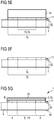
- FIG. 5 is a method for producing an organic optoelectronic device, for example according to FIG. 4 , illustrated.
- the first electrode 11 is applied to the main side 20 of the carrier 2.
- the first electrode 11 is indium tin oxide, ITO for short.
- FIG. 5B is illustrated that on a main surface 6 of the first electrode 11, a photosensitive material 9 is applied and in particular also developed.
- a thickness of the photosensitive material 9 is, for example, about 2 ⁇ m.
- the photosensitive material 9 is preferably a positive resist, English positive resist. That is, by exposure, the photosensitive material 9 is at least partially destroyed or made soluble for certain solvents particularly after development.
- the photosensitive material is, for example, AZ 1518 or OCG 825. Developer for the photosensitive material is, for example, MIF 350.
- the exposure is preferably carried out with unfiltered ultraviolet radiation of a Hg high-pressure lamp or a HgXe high-pressure lamp with a Radiation power of about 4 mW / cm 2 and an exposure time of about 20 s. The exposure takes place only outside a zone 13 of the first electrode 11. In FIG. 5B the exposure is illustrated by arrows.
- the photosensitive material 9 is subsequently removed.
- removing the photosensitive material 9 there is no or no significant material removal with respect to the first electrode 11.
- a thickness of the first electrode 11 is in a direction perpendicular to the main side 20 of the support 2, not affected by the removal of the photosensitive material 9.
- the removal is preferably carried out by ashing with an oxygen plasma and by rinsing with a solvent, for example a glycol ester.
- another photosensitive material 14 is applied and preferably also developed.
- the further light-sensitive material 14 may also be a positive photoresist. Outside a sub-area 15, the other photosensitive material 14 is also exposed, illustrated by arrows.
- the region in which the sub-region 15 and the zone 13 overlap constitutes an overlap region 16.
- the photosensitive material 9 and the further photosensitive material 14 were preferably developed, but not exposed.
- the other photosensitive material outside the subregion 15 is removed.
- the first electrode 11 is removed.
- a structuring of the first electrode 11 takes place by a material removal of a material of the first electrode 11. In particular, at least in places the main side 20 of the carrier 2 is exposed.
- the further photosensitive material 14 is then removed without changing a thickness of the first electrode 11 in the lower region 15.
- the work function of the first electrode 11 is reduced on the main surface 6 of the first electrode 11 in the overlap region 16, as compared to the first electrode 11 outside the overlap region 16.
- the organic optoelectronic component 1 is completed, see FIG. 5G .
- the organic layer sequence 3 with the at least one organic active layer 33 and the second electrode 22 are applied.
- the application can only take place over the first electrode 11 or, unlike in FIG FIG. 5G shown, also made over the entire surface.
- FIG. 5G it is possible that further, in FIG. 5G not shown, for example, for encapsulation of the organic optoelectronic device 1 and in particular the organic layer sequence 3 are applied. Furthermore, it is optionally possible for an antireflection coating to be applied to the radiation passage area 17, for example.
Landscapes
- Engineering & Computer Science (AREA)
- Chemical & Material Sciences (AREA)
- Nanotechnology (AREA)
- Physics & Mathematics (AREA)
- Life Sciences & Earth Sciences (AREA)
- Biophysics (AREA)
- Optics & Photonics (AREA)
- Crystallography & Structural Chemistry (AREA)
- Manufacturing & Machinery (AREA)
- Electroluminescent Light Sources (AREA)
Applications Claiming Priority (3)
| Application Number | Priority Date | Filing Date | Title |
|---|---|---|---|
| DE102009015574 | 2009-03-30 | ||
| DE102009022902.7A DE102009022902B4 (de) | 2009-03-30 | 2009-05-27 | Organisches optoelektronisches Bauteil und Verfahren zur Herstellung eines organischen optoelektronischen Bauteils |
| PCT/EP2010/053844 WO2010112381A1 (de) | 2009-03-30 | 2010-03-24 | Organisches optoelektronisches bauteil und verfahren zur herstellung eines organischen optoelektronischen bauteils |
Publications (2)
| Publication Number | Publication Date |
|---|---|
| EP2414887A1 EP2414887A1 (de) | 2012-02-08 |
| EP2414887B1 true EP2414887B1 (de) | 2017-12-06 |
Family
ID=42675105
Family Applications (1)
| Application Number | Title | Priority Date | Filing Date |
|---|---|---|---|
| EP10712396.0A Active EP2414887B1 (de) | 2009-03-30 | 2010-03-24 | Verfahren zur herstellung eines organischen optoelektronischen bauteils |
Country Status (7)
| Country | Link |
|---|---|
| US (1) | US9466797B2 (https=) |
| EP (1) | EP2414887B1 (https=) |
| JP (1) | JP5623501B2 (https=) |
| KR (1) | KR101617487B1 (https=) |
| CN (1) | CN102362213B (https=) |
| DE (1) | DE102009022902B4 (https=) |
| WO (1) | WO2010112381A1 (https=) |
Families Citing this family (5)
| Publication number | Priority date | Publication date | Assignee | Title |
|---|---|---|---|---|
| DE102012200084B4 (de) | 2012-01-04 | 2021-05-12 | Pictiva Displays International Limited | Strahlungsemittierendes organisches bauteil |
| DE102013110666B4 (de) | 2013-09-26 | 2023-05-17 | Pictiva Displays International Limited | Strahlungsemittierende Vorrichtung und Verfahren zur Herstellung derselben |
| DE102016214743B4 (de) * | 2016-08-09 | 2025-10-30 | Pictiva Displays International Limited | Optoelektronische Vorrichtung |
| CN110416259A (zh) * | 2018-04-26 | 2019-11-05 | 矽碁科技股份有限公司 | 用于显示静态图案的显示装置以及其制作方法与礼盒 |
| CN116314597B (zh) * | 2023-05-23 | 2023-08-08 | 珠海冠宇动力电池有限公司 | 一种电池和电子设备 |
Citations (1)
| Publication number | Priority date | Publication date | Assignee | Title |
|---|---|---|---|---|
| EP1684550A1 (en) * | 2003-10-02 | 2006-07-26 | Kabushiki Kaisha Toyota Jidoshokki | Electric field light emitting element |
Family Cites Families (40)
| Publication number | Priority date | Publication date | Assignee | Title |
|---|---|---|---|---|
| US6939625B2 (en) * | 1996-06-25 | 2005-09-06 | Nôrthwestern University | Organic light-emitting diodes and methods for assembly and enhanced charge injection |
| US5902688A (en) | 1996-07-16 | 1999-05-11 | Hewlett-Packard Company | Electroluminescent display device |
| US6407783B1 (en) * | 1998-04-07 | 2002-06-18 | Optrex Corporation | Liquid crystal display device |
| TW465119B (en) | 1999-07-23 | 2001-11-21 | Semiconductor Energy Lab | EL display device and a method of manufacturing the same |
| JP2001093314A (ja) * | 1999-09-20 | 2001-04-06 | Mitsubishi Chemicals Corp | 面光源装置及びこれを用いた液晶ディスプレイ装置 |
| US20020175620A1 (en) * | 2000-04-06 | 2002-11-28 | Osamu Yokoyama | Organic EL device and display panel incorporating the organic EL device |
| US6501218B1 (en) * | 2000-06-12 | 2002-12-31 | General Electric Company | Outdoor electroluminescent display devices |
| JP2008186815A (ja) * | 2001-03-23 | 2008-08-14 | Mitsubishi Chemicals Corp | 薄膜型発光体及びその製造方法 |
| KR100581850B1 (ko) | 2002-02-27 | 2006-05-22 | 삼성에스디아이 주식회사 | 유기 전계 발광 표시 장치와 그 제조 방법 |
| JP2003282274A (ja) * | 2002-03-25 | 2003-10-03 | Dainippon Printing Co Ltd | El電極の製造方法 |
| US6699829B2 (en) * | 2002-06-07 | 2004-03-02 | Kyzen Corporation | Cleaning compositions containing dichloroethylene and six carbon alkoxy substituted perfluoro compounds |
| GB0218202D0 (en) * | 2002-08-06 | 2002-09-11 | Avecia Ltd | Organic light emitting diodes |
| JP4447203B2 (ja) * | 2002-09-05 | 2010-04-07 | 大日本印刷株式会社 | パターン形成体 |
| DE10308515B4 (de) | 2003-02-26 | 2007-01-25 | Schott Ag | Verfahren zur Herstellung organischer lichtemittierender Dioden und organische lichtemittierende Diode |
| US6995445B2 (en) * | 2003-03-14 | 2006-02-07 | The Trustees Of Princeton University | Thin film organic position sensitive detectors |
| WO2004084324A1 (de) * | 2003-03-19 | 2004-09-30 | Osram Opto Semiconductors | Organische leuchtdiode mit integriertem bild |
| JP4242203B2 (ja) * | 2003-05-09 | 2009-03-25 | ローム株式会社 | 有機el表示装置 |
| TWI260945B (en) * | 2003-05-16 | 2006-08-21 | Toyota Ind Corp | Light-emitting apparatus and method for forming the same |
| US6955939B1 (en) * | 2003-11-03 | 2005-10-18 | Advanced Micro Devices, Inc. | Memory element formation with photosensitive polymer dielectric |
| JP2005215563A (ja) * | 2004-01-30 | 2005-08-11 | Kawaguchiko Seimitsu Co Ltd | 表示装置 |
| JP4526115B2 (ja) * | 2004-05-24 | 2010-08-18 | ソニーケミカル&インフォメーションデバイス株式会社 | フレキシブルフラットケーブル |
| JP2005339893A (ja) * | 2004-05-25 | 2005-12-08 | Sharp Corp | 有機el素子 |
| JP2005339383A (ja) | 2004-05-28 | 2005-12-08 | Ricoh Co Ltd | 印刷システム |
| CN102064102B (zh) * | 2004-06-08 | 2013-10-30 | 桑迪士克公司 | 形成单层纳米结构的方法和器件以及包含这种单层的器件 |
| JP2006318876A (ja) * | 2004-06-29 | 2006-11-24 | Dainippon Printing Co Ltd | エレクトロルミネッセント素子の製造方法及びエレクトロルミネッセント素子 |
| JP2006107996A (ja) | 2004-10-07 | 2006-04-20 | Dainippon Printing Co Ltd | 発光表示パネル |
| US20090082499A1 (en) * | 2004-11-16 | 2009-03-26 | Mitsubishi Plastics, Inc. | Aliphatic polyester-based resin reflective film and reflective plate |
| EP1835513A4 (en) | 2004-12-27 | 2011-11-09 | Fujikura Ltd | ELECTRONIC DEVICE AND METHOD FOR THE PRODUCTION THEREOF |
| WO2006090838A1 (ja) * | 2005-02-25 | 2006-08-31 | Nissan Motor Co., Ltd. | 有機エレクトロルミネッセント素子及びその製造方法 |
| JP2006294261A (ja) | 2005-04-05 | 2006-10-26 | Fuji Electric Holdings Co Ltd | 有機el発光素子およびその製造方法 |
| WO2006116584A2 (en) * | 2005-04-27 | 2006-11-02 | Dynamic Organic Light, Inc. | Light emitting polymer devices using self-assembled monolayer structures |
| US20070020482A1 (en) * | 2005-07-19 | 2007-01-25 | Osram-Opto Semiconductors Gmbh | Surface-selective deposition of organic thin films |
| JP2007123377A (ja) * | 2005-10-26 | 2007-05-17 | Matsushita Electric Ind Co Ltd | 有機半導体素子モジュール |
| JP4808479B2 (ja) * | 2005-11-28 | 2011-11-02 | 大日本印刷株式会社 | 有機発光トランジスタ素子及びその製造方法並びに発光表示装置 |
| DE102006000993B4 (de) | 2006-01-05 | 2010-12-02 | Merck Patent Gmbh | OLEDs mit erhöhter Licht-Auskopplung |
| EP1987702A2 (fr) * | 2006-02-22 | 2008-11-05 | Saint-Gobain Glass France | Dispositif electroluminescent organique et utilisation d'une couche electroconductrice transparente dans un dispositif electroluminescent organique |
| JP2007273397A (ja) * | 2006-03-31 | 2007-10-18 | Pioneer Electronic Corp | 有機el多色ディスプレイパネル |
| JP2007323814A (ja) * | 2006-05-30 | 2007-12-13 | Dainippon Printing Co Ltd | エリア発光型有機el表示パネルおよび階調制御方法 |
| TWI323047B (en) * | 2006-11-28 | 2010-04-01 | Univ Nat Taiwan | The method for forming electronic devices by using protection layers |
| CN101552241B (zh) * | 2008-04-03 | 2010-11-03 | 北京京东方光电科技有限公司 | 阵列基板及其制造方法和液晶显示装置 |
-
2009
- 2009-05-27 DE DE102009022902.7A patent/DE102009022902B4/de active Active
-
2010
- 2010-03-24 US US13/260,982 patent/US9466797B2/en active Active
- 2010-03-24 JP JP2012502578A patent/JP5623501B2/ja not_active Expired - Fee Related
- 2010-03-24 WO PCT/EP2010/053844 patent/WO2010112381A1/de not_active Ceased
- 2010-03-24 KR KR1020117025781A patent/KR101617487B1/ko not_active Expired - Fee Related
- 2010-03-24 EP EP10712396.0A patent/EP2414887B1/de active Active
- 2010-03-24 CN CN201080013281.4A patent/CN102362213B/zh not_active Expired - Fee Related
Patent Citations (1)
| Publication number | Priority date | Publication date | Assignee | Title |
|---|---|---|---|---|
| EP1684550A1 (en) * | 2003-10-02 | 2006-07-26 | Kabushiki Kaisha Toyota Jidoshokki | Electric field light emitting element |
Also Published As
| Publication number | Publication date |
|---|---|
| KR20120013354A (ko) | 2012-02-14 |
| KR101617487B1 (ko) | 2016-05-02 |
| EP2414887A1 (de) | 2012-02-08 |
| WO2010112381A1 (de) | 2010-10-07 |
| JP2012522345A (ja) | 2012-09-20 |
| US20120132894A1 (en) | 2012-05-31 |
| DE102009022902A1 (de) | 2010-10-07 |
| DE102009022902B4 (de) | 2023-10-26 |
| JP5623501B2 (ja) | 2014-11-12 |
| CN102362213A (zh) | 2012-02-22 |
| CN102362213B (zh) | 2015-06-03 |
| US9466797B2 (en) | 2016-10-11 |
Similar Documents
| Publication | Publication Date | Title |
|---|---|---|
| DE69735483T3 (de) | Organisches lichtemittierendes bauelement und dessen herstellung | |
| DE102007060108B4 (de) | Verfahren zur Herstellung eines Solarzellenmoduls | |
| DE60314610T2 (de) | Verfahren zur herstellung von organischen optoelektronischen und elektronischen bauteilen sowie dadurch erhaltene bauteile | |
| EP2356711B1 (de) | Organische leuchtdiode mit optischem resonator nebst herstellungsverfahren | |
| JP4124379B2 (ja) | 有機エレクトロルミネセンス素子 | |
| EP2414887B1 (de) | Verfahren zur herstellung eines organischen optoelektronischen bauteils | |
| EP2272116B1 (de) | Lichtemittierendes organisches bauelement und anordnung mit mehreren lichtemittierenden organischen bauelementen | |
| WO2010025696A2 (de) | Verfahren zur herstellung eines organischen strahlungsemittierenden bauelements und organisches strahlungsemittierendes bauelement | |
| DE102012200084B4 (de) | Strahlungsemittierendes organisches bauteil | |
| DE102016122901A1 (de) | Optoelektronisches Bauelement und Verfahren zum Herstellen eines optoelektronischen Bauelements | |
| EP1738423A1 (de) | Organisches, elektro-optisches element mit erhöhter auskoppeleffizienz | |
| WO2015124629A1 (de) | Organisches lichtemittierendes bauelement | |
| DE112005003229T5 (de) | Organische elektrolumineszierende Vorrichtung | |
| EP2702620B1 (de) | Lichtabgebendes element mit einer oled oder qled | |
| EP2165378A1 (de) | Organisches, weisslicht nach oben emittierendes bauelement | |
| DE102015212477B4 (de) | Organisches lichtemittierendes Bauelement und Verfahren zur Herstellung eines organischen lichtemittierenden Bauelements | |
| DE102008015697A1 (de) | Verfahren zur Herstellung eines strukturierten optoelektronischen Bauelementes und Anordnung zur Durchführung eines solchen | |
| EP1983593B1 (de) | Organisches optoelektronisches Bauelement | |
| DE112015007270B4 (de) | Optoelektronische Vorrichtung mit Schmelzsicherung | |
| DE112016002042B4 (de) | Lichtemittierendes bauelement und verfahren zur herstellung eines lichtemittierenden bauelements | |
| DE102012021691B4 (de) | Verfahren zur Herstellung von organischen Leuchtdioden oder organischen photovoltaischen Elementen | |
| DE102008021655B4 (de) | Strahlungsquelle und Solarzelle | |
| DE102015114167B4 (de) | Leuchtdiode und Verfahren zur Herstellung einer Leuchtdiode | |
| DE102017102689B4 (de) | Organisches Licht emittierendes Bauelement und Verfahren zur Herstellung eines organischen Licht emittierenden Bauelements | |
| DE102015106630A1 (de) | Organisches lichtemittierendes Bauelement und Verfahren zur Herstellung eines organischen lichtemittierenden Bauelements |
Legal Events
| Date | Code | Title | Description |
|---|---|---|---|
| PUAI | Public reference made under article 153(3) epc to a published international application that has entered the european phase |
Free format text: ORIGINAL CODE: 0009012 |
|
| 17P | Request for examination filed |
Effective date: 20110523 |
|
| AK | Designated contracting states |
Kind code of ref document: A1 Designated state(s): AT BE BG CH CY CZ DE DK EE ES FI FR GB GR HR HU IE IS IT LI LT LU LV MC MK MT NL NO PL PT RO SE SI SK SM TR |
|
| DAX | Request for extension of the european patent (deleted) | ||
| RAP1 | Party data changed (applicant data changed or rights of an application transferred) |
Owner name: OSRAM OLED GMBH |
|
| REG | Reference to a national code |
Ref country code: DE Ref legal event code: R079 Ref document number: 502010014449 Country of ref document: DE Free format text: PREVIOUS MAIN CLASS: G02F0001000000 Ipc: B82Y0020000000 |
|
| GRAP | Despatch of communication of intention to grant a patent |
Free format text: ORIGINAL CODE: EPIDOSNIGR1 |
|
| RIC1 | Information provided on ipc code assigned before grant |
Ipc: H01L 51/00 20060101ALI20170803BHEP Ipc: H01L 51/52 20060101ALN20170803BHEP Ipc: H01L 51/50 20060101ALN20170803BHEP Ipc: B82Y 20/00 20110101AFI20170803BHEP Ipc: H01L 27/32 20060101ALI20170803BHEP |
|
| INTG | Intention to grant announced |
Effective date: 20170822 |
|
| GRAS | Grant fee paid |
Free format text: ORIGINAL CODE: EPIDOSNIGR3 |
|
| GRAA | (expected) grant |
Free format text: ORIGINAL CODE: 0009210 |
|
| AK | Designated contracting states |
Kind code of ref document: B1 Designated state(s): AT BE BG CH CY CZ DE DK EE ES FI FR GB GR HR HU IE IS IT LI LT LU LV MC MK MT NL NO PL PT RO SE SI SK SM TR |
|
| REG | Reference to a national code |
Ref country code: GB Ref legal event code: FG4D Free format text: NOT ENGLISH |
|
| REG | Reference to a national code |
Ref country code: AT Ref legal event code: REF Ref document number: 952197 Country of ref document: AT Kind code of ref document: T Effective date: 20171215 Ref country code: CH Ref legal event code: EP |
|
| REG | Reference to a national code |
Ref country code: IE Ref legal event code: FG4D Free format text: LANGUAGE OF EP DOCUMENT: GERMAN |
|
| REG | Reference to a national code |
Ref country code: DE Ref legal event code: R096 Ref document number: 502010014449 Country of ref document: DE |
|
| REG | Reference to a national code |
Ref country code: NL Ref legal event code: MP Effective date: 20171206 |
|
| REG | Reference to a national code |
Ref country code: LT Ref legal event code: MG4D |
|
| PG25 | Lapsed in a contracting state [announced via postgrant information from national office to epo] |
Ref country code: SE Free format text: LAPSE BECAUSE OF FAILURE TO SUBMIT A TRANSLATION OF THE DESCRIPTION OR TO PAY THE FEE WITHIN THE PRESCRIBED TIME-LIMIT Effective date: 20171206 Ref country code: FI Free format text: LAPSE BECAUSE OF FAILURE TO SUBMIT A TRANSLATION OF THE DESCRIPTION OR TO PAY THE FEE WITHIN THE PRESCRIBED TIME-LIMIT Effective date: 20171206 Ref country code: LT Free format text: LAPSE BECAUSE OF FAILURE TO SUBMIT A TRANSLATION OF THE DESCRIPTION OR TO PAY THE FEE WITHIN THE PRESCRIBED TIME-LIMIT Effective date: 20171206 Ref country code: NO Free format text: LAPSE BECAUSE OF FAILURE TO SUBMIT A TRANSLATION OF THE DESCRIPTION OR TO PAY THE FEE WITHIN THE PRESCRIBED TIME-LIMIT Effective date: 20180306 Ref country code: ES Free format text: LAPSE BECAUSE OF FAILURE TO SUBMIT A TRANSLATION OF THE DESCRIPTION OR TO PAY THE FEE WITHIN THE PRESCRIBED TIME-LIMIT Effective date: 20171206 |
|
| PG25 | Lapsed in a contracting state [announced via postgrant information from national office to epo] |
Ref country code: GR Free format text: LAPSE BECAUSE OF FAILURE TO SUBMIT A TRANSLATION OF THE DESCRIPTION OR TO PAY THE FEE WITHIN THE PRESCRIBED TIME-LIMIT Effective date: 20180307 Ref country code: BG Free format text: LAPSE BECAUSE OF FAILURE TO SUBMIT A TRANSLATION OF THE DESCRIPTION OR TO PAY THE FEE WITHIN THE PRESCRIBED TIME-LIMIT Effective date: 20180306 Ref country code: LV Free format text: LAPSE BECAUSE OF FAILURE TO SUBMIT A TRANSLATION OF THE DESCRIPTION OR TO PAY THE FEE WITHIN THE PRESCRIBED TIME-LIMIT Effective date: 20171206 Ref country code: HR Free format text: LAPSE BECAUSE OF FAILURE TO SUBMIT A TRANSLATION OF THE DESCRIPTION OR TO PAY THE FEE WITHIN THE PRESCRIBED TIME-LIMIT Effective date: 20171206 |
|
| PG25 | Lapsed in a contracting state [announced via postgrant information from national office to epo] |
Ref country code: NL Free format text: LAPSE BECAUSE OF FAILURE TO SUBMIT A TRANSLATION OF THE DESCRIPTION OR TO PAY THE FEE WITHIN THE PRESCRIBED TIME-LIMIT Effective date: 20171206 |
|
| PG25 | Lapsed in a contracting state [announced via postgrant information from national office to epo] |
Ref country code: EE Free format text: LAPSE BECAUSE OF FAILURE TO SUBMIT A TRANSLATION OF THE DESCRIPTION OR TO PAY THE FEE WITHIN THE PRESCRIBED TIME-LIMIT Effective date: 20171206 Ref country code: SK Free format text: LAPSE BECAUSE OF FAILURE TO SUBMIT A TRANSLATION OF THE DESCRIPTION OR TO PAY THE FEE WITHIN THE PRESCRIBED TIME-LIMIT Effective date: 20171206 Ref country code: CZ Free format text: LAPSE BECAUSE OF FAILURE TO SUBMIT A TRANSLATION OF THE DESCRIPTION OR TO PAY THE FEE WITHIN THE PRESCRIBED TIME-LIMIT Effective date: 20171206 |
|
| PG25 | Lapsed in a contracting state [announced via postgrant information from national office to epo] |
Ref country code: IT Free format text: LAPSE BECAUSE OF FAILURE TO SUBMIT A TRANSLATION OF THE DESCRIPTION OR TO PAY THE FEE WITHIN THE PRESCRIBED TIME-LIMIT Effective date: 20171206 Ref country code: SM Free format text: LAPSE BECAUSE OF FAILURE TO SUBMIT A TRANSLATION OF THE DESCRIPTION OR TO PAY THE FEE WITHIN THE PRESCRIBED TIME-LIMIT Effective date: 20171206 Ref country code: RO Free format text: LAPSE BECAUSE OF FAILURE TO SUBMIT A TRANSLATION OF THE DESCRIPTION OR TO PAY THE FEE WITHIN THE PRESCRIBED TIME-LIMIT Effective date: 20171206 Ref country code: PL Free format text: LAPSE BECAUSE OF FAILURE TO SUBMIT A TRANSLATION OF THE DESCRIPTION OR TO PAY THE FEE WITHIN THE PRESCRIBED TIME-LIMIT Effective date: 20171206 |
|
| REG | Reference to a national code |
Ref country code: DE Ref legal event code: R097 Ref document number: 502010014449 Country of ref document: DE |
|
| PG25 | Lapsed in a contracting state [announced via postgrant information from national office to epo] |
Ref country code: MT Free format text: LAPSE BECAUSE OF FAILURE TO SUBMIT A TRANSLATION OF THE DESCRIPTION OR TO PAY THE FEE WITHIN THE PRESCRIBED TIME-LIMIT Effective date: 20171206 |
|
| PLBE | No opposition filed within time limit |
Free format text: ORIGINAL CODE: 0009261 |
|
| STAA | Information on the status of an ep patent application or granted ep patent |
Free format text: STATUS: NO OPPOSITION FILED WITHIN TIME LIMIT |
|
| REG | Reference to a national code |
Ref country code: CH Ref legal event code: PL |
|
| 26N | No opposition filed |
Effective date: 20180907 |
|
| GBPC | Gb: european patent ceased through non-payment of renewal fee |
Effective date: 20180324 |
|
| PG25 | Lapsed in a contracting state [announced via postgrant information from national office to epo] |
Ref country code: DK Free format text: LAPSE BECAUSE OF FAILURE TO SUBMIT A TRANSLATION OF THE DESCRIPTION OR TO PAY THE FEE WITHIN THE PRESCRIBED TIME-LIMIT Effective date: 20171206 Ref country code: MC Free format text: LAPSE BECAUSE OF FAILURE TO SUBMIT A TRANSLATION OF THE DESCRIPTION OR TO PAY THE FEE WITHIN THE PRESCRIBED TIME-LIMIT Effective date: 20171206 Ref country code: SI Free format text: LAPSE BECAUSE OF FAILURE TO SUBMIT A TRANSLATION OF THE DESCRIPTION OR TO PAY THE FEE WITHIN THE PRESCRIBED TIME-LIMIT Effective date: 20171206 |
|
| REG | Reference to a national code |
Ref country code: BE Ref legal event code: MM Effective date: 20180331 |
|
| REG | Reference to a national code |
Ref country code: IE Ref legal event code: MM4A |
|
| PG25 | Lapsed in a contracting state [announced via postgrant information from national office to epo] |
Ref country code: LU Free format text: LAPSE BECAUSE OF NON-PAYMENT OF DUE FEES Effective date: 20180324 |
|
| PG25 | Lapsed in a contracting state [announced via postgrant information from national office to epo] |
Ref country code: IE Free format text: LAPSE BECAUSE OF NON-PAYMENT OF DUE FEES Effective date: 20180324 |
|
| PG25 | Lapsed in a contracting state [announced via postgrant information from national office to epo] |
Ref country code: LI Free format text: LAPSE BECAUSE OF NON-PAYMENT OF DUE FEES Effective date: 20180331 Ref country code: CH Free format text: LAPSE BECAUSE OF NON-PAYMENT OF DUE FEES Effective date: 20180331 Ref country code: GB Free format text: LAPSE BECAUSE OF NON-PAYMENT OF DUE FEES Effective date: 20180324 Ref country code: BE Free format text: LAPSE BECAUSE OF NON-PAYMENT OF DUE FEES Effective date: 20180331 |
|
| PG25 | Lapsed in a contracting state [announced via postgrant information from national office to epo] |
Ref country code: FR Free format text: LAPSE BECAUSE OF NON-PAYMENT OF DUE FEES Effective date: 20180331 |
|
| REG | Reference to a national code |
Ref country code: AT Ref legal event code: MM01 Ref document number: 952197 Country of ref document: AT Kind code of ref document: T Effective date: 20180324 |
|
| PG25 | Lapsed in a contracting state [announced via postgrant information from national office to epo] |
Ref country code: AT Free format text: LAPSE BECAUSE OF NON-PAYMENT OF DUE FEES Effective date: 20180324 |
|
| PG25 | Lapsed in a contracting state [announced via postgrant information from national office to epo] |
Ref country code: TR Free format text: LAPSE BECAUSE OF FAILURE TO SUBMIT A TRANSLATION OF THE DESCRIPTION OR TO PAY THE FEE WITHIN THE PRESCRIBED TIME-LIMIT Effective date: 20171206 |
|
| PG25 | Lapsed in a contracting state [announced via postgrant information from national office to epo] |
Ref country code: HU Free format text: LAPSE BECAUSE OF FAILURE TO SUBMIT A TRANSLATION OF THE DESCRIPTION OR TO PAY THE FEE WITHIN THE PRESCRIBED TIME-LIMIT; INVALID AB INITIO Effective date: 20100324 Ref country code: PT Free format text: LAPSE BECAUSE OF FAILURE TO SUBMIT A TRANSLATION OF THE DESCRIPTION OR TO PAY THE FEE WITHIN THE PRESCRIBED TIME-LIMIT Effective date: 20171206 |
|
| PG25 | Lapsed in a contracting state [announced via postgrant information from national office to epo] |
Ref country code: MK Free format text: LAPSE BECAUSE OF NON-PAYMENT OF DUE FEES Effective date: 20171206 Ref country code: CY Free format text: LAPSE BECAUSE OF FAILURE TO SUBMIT A TRANSLATION OF THE DESCRIPTION OR TO PAY THE FEE WITHIN THE PRESCRIBED TIME-LIMIT Effective date: 20171206 |
|
| PG25 | Lapsed in a contracting state [announced via postgrant information from national office to epo] |
Ref country code: IS Free format text: LAPSE BECAUSE OF FAILURE TO SUBMIT A TRANSLATION OF THE DESCRIPTION OR TO PAY THE FEE WITHIN THE PRESCRIBED TIME-LIMIT Effective date: 20180406 |
|
| REG | Reference to a national code |
Ref country code: DE Ref legal event code: R081 Ref document number: 502010014449 Country of ref document: DE Owner name: PICTIVA DISPLAYS INTERNATIONAL LIMITED, IE Free format text: FORMER OWNER: OSRAM OLED GMBH, 93049 REGENSBURG, DE Ref country code: DE Ref legal event code: R082 Ref document number: 502010014449 Country of ref document: DE Representative=s name: EPPING HERMANN FISCHER PATENTANWALTSGESELLSCHA, DE |
|
| PGFP | Annual fee paid to national office [announced via postgrant information from national office to epo] |
Ref country code: DE Payment date: 20260323 Year of fee payment: 17 |