EP2414887B1 - Method for producing an organic optoelectronic component - Google Patents
Method for producing an organic optoelectronic component Download PDFInfo
- Publication number
- EP2414887B1 EP2414887B1 EP10712396.0A EP10712396A EP2414887B1 EP 2414887 B1 EP2414887 B1 EP 2414887B1 EP 10712396 A EP10712396 A EP 10712396A EP 2414887 B1 EP2414887 B1 EP 2414887B1
- Authority
- EP
- European Patent Office
- Prior art keywords
- electrode
- organic
- region
- light
- carrier
- Prior art date
- Legal status (The legal status is an assumption and is not a legal conclusion. Google has not performed a legal analysis and makes no representation as to the accuracy of the status listed.)
- Active
Links
- 230000005693 optoelectronics Effects 0.000 title claims description 36
- 238000004519 manufacturing process Methods 0.000 title claims description 14
- 239000000463 material Substances 0.000 claims description 76
- 239000010410 layer Substances 0.000 claims description 46
- 239000012044 organic layer Substances 0.000 claims description 38
- 238000000034 method Methods 0.000 claims description 23
- AMGQUBHHOARCQH-UHFFFAOYSA-N indium;oxotin Chemical compound [In].[Sn]=O AMGQUBHHOARCQH-UHFFFAOYSA-N 0.000 claims description 8
- 229920002120 photoresistant polymer Polymers 0.000 claims description 7
- 230000005855 radiation Effects 0.000 description 53
- 239000002356 single layer Substances 0.000 description 35
- 238000002310 reflectometry Methods 0.000 description 30
- 238000007788 roughening Methods 0.000 description 19
- UHOVQNZJYSORNB-UHFFFAOYSA-N Benzene Chemical compound C1=CC=CC=C1 UHOVQNZJYSORNB-UHFFFAOYSA-N 0.000 description 6
- 239000002800 charge carrier Substances 0.000 description 5
- 239000011521 glass Substances 0.000 description 5
- VYPSYNLAJGMNEJ-UHFFFAOYSA-N silicon dioxide Inorganic materials O=[Si]=O VYPSYNLAJGMNEJ-UHFFFAOYSA-N 0.000 description 5
- 230000003595 spectral effect Effects 0.000 description 5
- 230000005670 electromagnetic radiation Effects 0.000 description 4
- 229910052751 metal Inorganic materials 0.000 description 4
- 239000002184 metal Substances 0.000 description 4
- 238000010521 absorption reaction Methods 0.000 description 3
- 230000005540 biological transmission Effects 0.000 description 3
- 239000011248 coating agent Substances 0.000 description 3
- 238000000576 coating method Methods 0.000 description 3
- 235000012239 silicon dioxide Nutrition 0.000 description 3
- 239000002904 solvent Substances 0.000 description 3
- RGSFGYAAUTVSQA-UHFFFAOYSA-N Cyclopentane Chemical compound C1CCCC1 RGSFGYAAUTVSQA-UHFFFAOYSA-N 0.000 description 2
- 229910000831 Steel Inorganic materials 0.000 description 2
- XLOMVQKBTHCTTD-UHFFFAOYSA-N Zinc monoxide Chemical compound [Zn]=O XLOMVQKBTHCTTD-UHFFFAOYSA-N 0.000 description 2
- 238000004380 ashing Methods 0.000 description 2
- 230000015572 biosynthetic process Effects 0.000 description 2
- 125000001495 ethyl group Chemical group [H]C([H])([H])C([H])([H])* 0.000 description 2
- 239000011888 foil Substances 0.000 description 2
- 238000012986 modification Methods 0.000 description 2
- 230000004048 modification Effects 0.000 description 2
- 230000003287 optical effect Effects 0.000 description 2
- 239000000377 silicon dioxide Substances 0.000 description 2
- 239000010959 steel Substances 0.000 description 2
- YVTHLONGBIQYBO-UHFFFAOYSA-N zinc indium(3+) oxygen(2-) Chemical compound [O--].[Zn++].[In+3] YVTHLONGBIQYBO-UHFFFAOYSA-N 0.000 description 2
- OYPRJOBELJOOCE-UHFFFAOYSA-N Calcium Chemical compound [Ca] OYPRJOBELJOOCE-UHFFFAOYSA-N 0.000 description 1
- WHXSMMKQMYFTQS-UHFFFAOYSA-N Lithium Chemical compound [Li] WHXSMMKQMYFTQS-UHFFFAOYSA-N 0.000 description 1
- FYYHWMGAXLPEAU-UHFFFAOYSA-N Magnesium Chemical compound [Mg] FYYHWMGAXLPEAU-UHFFFAOYSA-N 0.000 description 1
- BPQQTUXANYXVAA-UHFFFAOYSA-N Orthosilicate Chemical group [O-][Si]([O-])([O-])[O-] BPQQTUXANYXVAA-UHFFFAOYSA-N 0.000 description 1
- BQCADISMDOOEFD-UHFFFAOYSA-N Silver Chemical compound [Ag] BQCADISMDOOEFD-UHFFFAOYSA-N 0.000 description 1
- GWEVSGVZZGPLCZ-UHFFFAOYSA-N Titan oxide Chemical compound O=[Ti]=O GWEVSGVZZGPLCZ-UHFFFAOYSA-N 0.000 description 1
- 239000002253 acid Substances 0.000 description 1
- 125000001931 aliphatic group Chemical group 0.000 description 1
- 229910052782 aluminium Inorganic materials 0.000 description 1
- XAGFODPZIPBFFR-UHFFFAOYSA-N aluminium Chemical compound [Al] XAGFODPZIPBFFR-UHFFFAOYSA-N 0.000 description 1
- 239000006117 anti-reflective coating Substances 0.000 description 1
- QVGXLLKOCUKJST-UHFFFAOYSA-N atomic oxygen Chemical compound [O] QVGXLLKOCUKJST-UHFFFAOYSA-N 0.000 description 1
- 229910052788 barium Inorganic materials 0.000 description 1
- DSAJWYNOEDNPEQ-UHFFFAOYSA-N barium atom Chemical compound [Ba] DSAJWYNOEDNPEQ-UHFFFAOYSA-N 0.000 description 1
- CXKCTMHTOKXKQT-UHFFFAOYSA-N cadmium oxide Inorganic materials [Cd]=O CXKCTMHTOKXKQT-UHFFFAOYSA-N 0.000 description 1
- CFEAAQFZALKQPA-UHFFFAOYSA-N cadmium(2+);oxygen(2-) Chemical compound [O-2].[Cd+2] CFEAAQFZALKQPA-UHFFFAOYSA-N 0.000 description 1
- 229910052791 calcium Inorganic materials 0.000 description 1
- 239000011575 calcium Substances 0.000 description 1
- 125000002915 carbonyl group Chemical group [*:2]C([*:1])=O 0.000 description 1
- 230000015556 catabolic process Effects 0.000 description 1
- 238000010276 construction Methods 0.000 description 1
- 230000001419 dependent effect Effects 0.000 description 1
- 239000002019 doping agent Substances 0.000 description 1
- 238000005538 encapsulation Methods 0.000 description 1
- 238000005530 etching Methods 0.000 description 1
- LYCAIKOWRPUZTN-UHFFFAOYSA-N ethylene glycol Natural products OCCO LYCAIKOWRPUZTN-UHFFFAOYSA-N 0.000 description 1
- 239000010408 film Substances 0.000 description 1
- -1 glycol ester Chemical class 0.000 description 1
- PCHJSUWPFVWCPO-UHFFFAOYSA-N gold Chemical compound [Au] PCHJSUWPFVWCPO-UHFFFAOYSA-N 0.000 description 1
- 229910052737 gold Inorganic materials 0.000 description 1
- 239000010931 gold Substances 0.000 description 1
- 238000000227 grinding Methods 0.000 description 1
- DMEGYFMYUHOHGS-UHFFFAOYSA-N heptamethylene Natural products C1CCCCCC1 DMEGYFMYUHOHGS-UHFFFAOYSA-N 0.000 description 1
- WGCNASOHLSPBMP-UHFFFAOYSA-N hydroxyacetaldehyde Natural products OCC=O WGCNASOHLSPBMP-UHFFFAOYSA-N 0.000 description 1
- 238000005286 illumination Methods 0.000 description 1
- 229910052738 indium Inorganic materials 0.000 description 1
- APFVFJFRJDLVQX-UHFFFAOYSA-N indium atom Chemical compound [In] APFVFJFRJDLVQX-UHFFFAOYSA-N 0.000 description 1
- 229910003437 indium oxide Inorganic materials 0.000 description 1
- PJXISJQVUVHSOJ-UHFFFAOYSA-N indium(iii) oxide Chemical compound [O-2].[O-2].[O-2].[In+3].[In+3] PJXISJQVUVHSOJ-UHFFFAOYSA-N 0.000 description 1
- 238000002347 injection Methods 0.000 description 1
- 239000007924 injection Substances 0.000 description 1
- 229910052744 lithium Inorganic materials 0.000 description 1
- 229910052749 magnesium Inorganic materials 0.000 description 1
- 239000011777 magnesium Substances 0.000 description 1
- 239000000203 mixture Substances 0.000 description 1
- 239000000178 monomer Substances 0.000 description 1
- 229920000620 organic polymer Polymers 0.000 description 1
- 229910052760 oxygen Inorganic materials 0.000 description 1
- 239000001301 oxygen Substances 0.000 description 1
- 125000002467 phosphate group Chemical group [H]OP(=O)(O[H])O[*] 0.000 description 1
- 238000004838 photoelectron emission spectroscopy Methods 0.000 description 1
- 239000004033 plastic Substances 0.000 description 1
- 239000002985 plastic film Substances 0.000 description 1
- 229920006255 plastic film Polymers 0.000 description 1
- 150000003222 pyridines Chemical class 0.000 description 1
- 239000010453 quartz Substances 0.000 description 1
- 238000007493 shaping process Methods 0.000 description 1
- 229910052710 silicon Inorganic materials 0.000 description 1
- 239000010703 silicon Substances 0.000 description 1
- 229910052709 silver Inorganic materials 0.000 description 1
- 239000004332 silver Substances 0.000 description 1
- 239000000758 substrate Substances 0.000 description 1
- XOLBLPGZBRYERU-UHFFFAOYSA-N tin dioxide Chemical compound O=[Sn]=O XOLBLPGZBRYERU-UHFFFAOYSA-N 0.000 description 1
- 229910001887 tin oxide Inorganic materials 0.000 description 1
- OGIDPMRJRNCKJF-UHFFFAOYSA-N titanium oxide Inorganic materials [Ti]=O OGIDPMRJRNCKJF-UHFFFAOYSA-N 0.000 description 1
- ZDHXKXAHOVTTAH-UHFFFAOYSA-N trichlorosilane Chemical group Cl[SiH](Cl)Cl ZDHXKXAHOVTTAH-UHFFFAOYSA-N 0.000 description 1
- 239000011787 zinc oxide Substances 0.000 description 1
Images


Classifications
-
- H—ELECTRICITY
- H10—SEMICONDUCTOR DEVICES; ELECTRIC SOLID-STATE DEVICES NOT OTHERWISE PROVIDED FOR
- H10K—ORGANIC ELECTRIC SOLID-STATE DEVICES
- H10K30/00—Organic devices sensitive to infrared radiation, light, electromagnetic radiation of shorter wavelength or corpuscular radiation
-
- H—ELECTRICITY
- H10—SEMICONDUCTOR DEVICES; ELECTRIC SOLID-STATE DEVICES NOT OTHERWISE PROVIDED FOR
- H10K—ORGANIC ELECTRIC SOLID-STATE DEVICES
- H10K71/00—Manufacture or treatment specially adapted for the organic devices covered by this subclass
- H10K71/621—Providing a shape to conductive layers, e.g. patterning or selective deposition
-
- B—PERFORMING OPERATIONS; TRANSPORTING
- B82—NANOTECHNOLOGY
- B82Y—SPECIFIC USES OR APPLICATIONS OF NANOSTRUCTURES; MEASUREMENT OR ANALYSIS OF NANOSTRUCTURES; MANUFACTURE OR TREATMENT OF NANOSTRUCTURES
- B82Y20/00—Nanooptics, e.g. quantum optics or photonic crystals
-
- H—ELECTRICITY
- H10—SEMICONDUCTOR DEVICES; ELECTRIC SOLID-STATE DEVICES NOT OTHERWISE PROVIDED FOR
- H10K—ORGANIC ELECTRIC SOLID-STATE DEVICES
- H10K59/00—Integrated devices, or assemblies of multiple devices, comprising at least one organic light-emitting element covered by group H10K50/00
- H10K59/10—OLED displays
- H10K59/221—Static displays, e.g. displaying permanent logos
-
- H—ELECTRICITY
- H10—SEMICONDUCTOR DEVICES; ELECTRIC SOLID-STATE DEVICES NOT OTHERWISE PROVIDED FOR
- H10K—ORGANIC ELECTRIC SOLID-STATE DEVICES
- H10K50/00—Organic light-emitting devices
- H10K50/10—OLEDs or polymer light-emitting diodes [PLED]
- H10K50/17—Carrier injection layers
-
- H—ELECTRICITY
- H10—SEMICONDUCTOR DEVICES; ELECTRIC SOLID-STATE DEVICES NOT OTHERWISE PROVIDED FOR
- H10K—ORGANIC ELECTRIC SOLID-STATE DEVICES
- H10K50/00—Organic light-emitting devices
- H10K50/80—Constructional details
- H10K50/85—Arrangements for extracting light from the devices
- H10K50/856—Arrangements for extracting light from the devices comprising reflective means
-
- Y—GENERAL TAGGING OF NEW TECHNOLOGICAL DEVELOPMENTS; GENERAL TAGGING OF CROSS-SECTIONAL TECHNOLOGIES SPANNING OVER SEVERAL SECTIONS OF THE IPC; TECHNICAL SUBJECTS COVERED BY FORMER USPC CROSS-REFERENCE ART COLLECTIONS [XRACs] AND DIGESTS
- Y02—TECHNOLOGIES OR APPLICATIONS FOR MITIGATION OR ADAPTATION AGAINST CLIMATE CHANGE
- Y02E—REDUCTION OF GREENHOUSE GAS [GHG] EMISSIONS, RELATED TO ENERGY GENERATION, TRANSMISSION OR DISTRIBUTION
- Y02E10/00—Energy generation through renewable energy sources
- Y02E10/50—Photovoltaic [PV] energy
- Y02E10/549—Organic PV cells
-
- Y—GENERAL TAGGING OF NEW TECHNOLOGICAL DEVELOPMENTS; GENERAL TAGGING OF CROSS-SECTIONAL TECHNOLOGIES SPANNING OVER SEVERAL SECTIONS OF THE IPC; TECHNICAL SUBJECTS COVERED BY FORMER USPC CROSS-REFERENCE ART COLLECTIONS [XRACs] AND DIGESTS
- Y02—TECHNOLOGIES OR APPLICATIONS FOR MITIGATION OR ADAPTATION AGAINST CLIMATE CHANGE
- Y02P—CLIMATE CHANGE MITIGATION TECHNOLOGIES IN THE PRODUCTION OR PROCESSING OF GOODS
- Y02P70/00—Climate change mitigation technologies in the production process for final industrial or consumer products
- Y02P70/50—Manufacturing or production processes characterised by the final manufactured product
Definitions
- a process for producing an organic optoelectronic component is specified.
- the publication GB 2 419 023 A concerns a display.
- a production process for an organic display can be found in the document JP 2006-294261 A , Herein, the work function of a metallic anode of an organic electroluminescent element of the organic display is increased by a UV-ozone treatment to form a high brightness organic display.
- the description of an electronic component and a corresponding manufacturing method thereof are in the document EP 1 835 513 A1 to find.
- EP 1 684 550 A1 discloses an organic electroluminescent element having light emitting and non-light emitting regions wherein the work function of an indium tin oxide anode is locally increased by UV treatment to form the light emitting regions.
- An object to be solved is to specify a method for producing an organic optoelectronic component which has bright areas and dark areas which are not externally distinguishable outside the operation of the organic optoelectronic component.
- an organic optoelectronic device which is also indicated below as an organic component or as a component.
- this has a carrier.
- the carrier serves to mechanically support the component.
- the support may comprise any of the following materials or be made of any of the following materials: glass, glass film, quartz, plastic, plastic film, metal, metal foil, silicon.
- the substrate is completely or partially transparent or translucent for an electromagnetic radiation to be emitted by the component.
- a first electrode is attached to the carrier.
- the first electrode may be in direct, direct contact with the carrier.
- at least one intermediate layer is applied in places or over the entire surface between the carrier and the first electrode.
- a surface property of the carrier can be adapted to the first electrode via the intermediate layer.
- the intermediate layer serves for an adhesion mediation between the carrier and the first electrode.
- a roughness of a surface of the carrier may be reduced via the intermediate layer. If an intermediate layer is present, it is preferably transparent or translucent with respect to the radiation to be emitted by the component.
- the first electrode is permeable to radiation, preferably transparent to the radiation to be emitted by the component.
- the first electrode is designed as an anode.
- the first electrode then serves as a hole-injecting material.
- the first electrode consists for example of a transparent conductive oxide. Suitable materials are including zinc oxide, tin oxide, cadmium oxide, titanium oxide, indium oxide, indium zinc oxide or indium tin oxide.
- the material of the first electrode may have dopants and be at least locally p-doped or n-doped.
- an organic layer sequence is applied to a main side of the first electrode facing away from the carrier.
- the organic layer sequence comprises at least one organic active layer.
- the active layer is designed to generate the electromagnetic radiation to be emitted during operation of the component.
- a wavelength of the radiation is in the spectral range between 200 nm and 3000 nm, preferably between 350 nm and 850 nm. In particular, visible radiation is generated during operation in the active layer.
- the organic layer sequence has, in addition to the at least one organic active layer, at least one charge carrier transport layer and / or one charge carrier injection layer and / or one charge carrier stop layer.
- the organic active layer comprises at least one organic polymer, an organic oligomer, an organic monomer, organic small non-polymeric molecules, or a combination thereof.
- a second electrode is applied to a side of the organic layer sequence facing away from the carrier.
- the organic layer sequence is thus located between the first electrode and the second electrode.
- the second electrode designed as a cathode.
- the second electrode comprises or consists of one of the following materials: aluminum, barium, indium, silver, gold, magnesium, calcium, lithium, steel.
- the second electrode is preferably impermeable and / or reflective for the radiation generated in the organic layer sequence. It is possible that the second electrode, in addition to the carrier, mechanically stabilizes the component.
- the latter has a radiation passage area.
- the radiation passage area may be a boundary surface of the component, through which the radiation generated in the active layer or a part or a large part of this radiation leaves the component.
- the radiation passage area is formed by a main side of the carrier facing away from the organic layer sequence.
- the radiation passage area can also be realized by an example antireflective coating on this main side of the carrier.
- the organic component at least one dark area and at least one bright area are formed in a lateral direction. Lateral means in particular along at least one main extension direction of the organic component.
- the bright area is an area of the radiation passage area of the component in which a greater radiation power is emitted per unit area than in the dark area.
- the bright area appears brighter than the dark area during operation of the component.
- This preferably has Component several light areas and several dark area on. The light areas and the dark areas are in each case contiguous areas of the radiation passage area of the component.
- the first and the second electrode as well as the organic layer sequence are applied to the carrier completely or in places in the at least one dark area as well as in the at least one bright area.
- both the bright region and the dark region with respect to the electrodes and the organic layer sequence have the same components.
- the second electrode and the organic layer sequence are manufactured identically both in the bright region and in the dark region, within the framework of the manufacturing tolerances.
- the first electrode is likewise a layer extending in particular throughout the dark region and the light region, with a preferably constant thickness within the scope of the manufacturing tolerances. That is, the structuring of the radiation passage area in light areas and dark areas is not achieved by a shaping or geometric configuration of the first electrode, the second electrode and the organic layer sequence.
- this has a first reflectivity of the dark region.
- the first reflectivity is a reflectivity of the radiation passage area in the dark area.
- the component has a second reflectivity of the bright region, which is, for example, a reflectivity of the radiation passage area in the bright region.
- the first reflectivity of the dark region deviates from the second reflectivity of the bright region by at most 15 percentage points, preferably by at most 10 percentage points, in particular by at most 5 percentage points from one another.
- a reflectivity at the radiation passage area in the bright area and a reflectivity at the radiation passage area in the dark area are approximately equal or, preferably, equal within the manufacturing tolerances.
- the reflectivity is, for example, in each case the quotient of an incident radiation power and a reflected, outgoing radiation power.
- the light output that strikes the radiation passage area is measured and compared with a light output reflected from the radiation passage area.
- the first reflectivity of the dark region is 15%
- the second reflectivity of the bright region is preferably between 10% and 20% inclusive.
- this comprises a carrier and a first electrode which is attached to the carrier. Furthermore, the component contains at least one organic layer sequence with at least one organic active layer. Furthermore, the component has a second electrode, so that the organic layer sequence is located between the first electrode and the second electrode. In a lateral direction, at least one dark area and at least one bright area are formed. Both in the Dark area as well as in the bright area is applied in places or over the entire surface both the first electrode and the second electrode and the organic layer sequence on the support. A first reflectivity of the dark area differs from a second reflectivity of the bright area by at most 15 percentage points.
- the at least one bright area and the at least one dark area By the at least one bright area and the at least one dark area, a pattern and / or a label and / or a symbol in the operation of the component can be displayed.
- the bright areas form bright, luminous areas about the pattern.
- the first reflectivity of the dark area and the second reflectivity of the bright area are approximately the same, it is possible that, for example, the pattern that is displayed during operation of the component is not visible outside the operation of the component.
- the radiation passage area of the component can be homogeneous and unstructured, if the component is not operated. That is, outside the operation of the component, the pattern is not recognizable by a viewer.
- a monolayer with self-organizing molecules is applied in the at least one dark region on a main surface of the first electrode facing away from the carrier.
- the monolayer is applied only in the dark area, so that the bright area is free of the monolayer.
- the entire dark area is covered by the monolayer.
- dark areas can be exclusively where, at the organic layer sequence, in particular in a direction perpendicular to the main surface of the first electrode, the monolayer is generated.
- Monolayer preferably means that a layer height of the molecules on the main side is only exactly one molecule. Accordingly, in the monolayer, preferably no identical molecules are superimposed.
- the monolayer is thus located between the first electrode and the organic layer sequence.
- the monolayer can be applied, for example, to the first electrode via a printing process.
- An achievable structure size of the monolayer, in a lateral direction is for example 100 ⁇ m, in particular 25 ⁇ m.
- the structure size is limited only by a spatial resolution of a printing process used for example when producing the monolayer. In other words, very fine patterns of the monolayer can be generated.
- the monolayer is colorless.
- an absorption coefficient and / or a reflection coefficient of the monolayer in the visible spectral range is approximately not dependent on the wavelength.
- the absorption coefficient and / or the reflection coefficient in the spectral range between 470 nm and 650 nm is constant except for a deviation of 10 percentage points, in particular to a deviation of 3 percentage points.
- the absorbency coefficient is between 0% and 10%, especially between 0.01% and 3% inclusive.
- the monolayer is electrically insulating. In one direction perpendicular to the first electrode is thus carried by the monolayer during operation of the component no current flow therethrough. If the organic layer sequence has a negligible electrical transverse conductivity, then radiation in the organic layer sequence is produced only in those areas in which no monolayer is applied.
- the monolayer preferably has a breakdown voltage of at least 1 MV / cm, in particular of at least 30 MV / cm, in a direction perpendicular to the first electrode.
- a thickness of the monolayer, in a direction perpendicular to the first electrode is between 0.5 nm and 5.0 nm, in particular between 1.0 nm and 3.0 nm.
- the monolayer is therefore very thin compared to a wavelength of radiation generated in the organic layer sequence. Therefore, the monolayer affects the optical properties of the component, in particular the optical refractive index, not or only negligible.
- the monolayer is formed with molecules or consists of those molecules which have long aliphatic chains and comprise a phosphate group, silicate group, carbonyl acid group, trichlorosilane group or a similar group as a head group.
- the molecules of the monolayer may also include large groups having a conjugated ring system, such as benzene or cyclopentane. Examples of such molecules are 2 [(trimethyloxysily) ethyl] benzene or 3- [2- (trimethyloxysily) ethyl] pyridines.
- the carrier has a roughening on a side facing the layer sequence in the dark region.
- the side of the carrier facing the layer sequence is approximately smooth in the bright region and deliberately rough in the dark region. The roughening is thus between the carrier and the first electrode.
- the radiation passage area in the context of the manufacturing tolerances, in the bright area as well as in the dark area has the same characteristics, for example with regard to roughness.
- the side of the carrier facing away from the organic layer sequence is not structured.
- an average roughness of the roughening is between 5 nm and 1 pm, in particular between 20 nm and 500 nm inclusive.
- the roughening thus has in particular an average roughness which is less than or equal to a wavelength in the organic Layer sequence generated radiation is.
- the roughening and / or the dark region has a lateral structure size of at least 1 mm, in particular of at least 3 mm.
- the roughening, and thus preferably also the dark area has an extent of at least the stated values in one or in two directions.
- the roughening can thus be formed flat.
- the roughening of the carrier in the dark region is formed by groove-like or channel-like structures which have a mean depth corresponding to the average roughness. Grooved may mean that an average length exceeds a mean width of the structures at least ten times.
- an intermediate layer is located between the carrier and the first electrode.
- the intermediate layer preferably has a refractive index which deviates from that of the carrier by at most 0.1, in particular by at most 0.05.
- the refractive index of the carrier is 1.50
- the refractive index of the intermediate layer is preferably between 1.45 and 1.55.
- the intermediate layer is an oxide layer, in particular a silicon dioxide layer.
- a thickness of the intermediate layer in a direction perpendicular to the first electrode, is between 10 nm and 200 nm inclusive, in particular between 15 nm and 40 nm inclusive. If the intermediate layer is applied over the roughening, then a Carrier side facing away from the intermediate layer preferably smoother than the carrier in the roughening.
- the average thickness of the intermediate layer may be in the range of the average roughness of the roughening of the carrier.
- an average radiation power per unit area of the at least one dark area is at most 60%, in particular at most 45%, of the mean radiation power per unit area of the at least one bright area. For example, approximately no radiant power is emitted in the dark region. It is also possible that the radiant power per area of the dark area is between 1% and 60% of that of the bright area, preferably between 2% and 45% inclusive, in particular between 4% and 30% inclusive.
- the carrier is designed with a glass, the first electrode with a conductive transparent oxide and the second electrode with a metal or consist of the materials mentioned.
- the radiation generated in the organic layer sequence thus passes through the carrier and is emitted, in particular, on a main side of the carrier facing away from the organic layer sequence.
- a main surface of the first electrode facing away from the carrier has a higher work function in the at least one dark region than in the at least one bright region.
- the work function is the minimum energy required to carry a charge carrier, such as an electron, from a point within the first electrode to a point outside the surface of the first electrode.
- the work function of the first electrode in the dark region differs from the work function in the light region by at least 0.10 eV, preferably by at least 0.25 eV, in particular by at least 0.40 eV.
- An absolute value of the work function here is preferably between 4.0 eV and 5.0 eV, in particular at about 4.5 eV.
- a modification of the work function is preferably not achieved in that a separate coating is applied, for example with a thin, in particular monolayer, layer of organic molecules. In other words, the first electrode is then free of such a separate, the work function affecting coating.
- an organic optoelectronic component can be produced, as described in connection with one or more of the abovementioned embodiments.
- Features of the organic optoelectronic component are therefore also disclosed for the method described here and vice versa.
- a photoresist is applied to the first electrode, and the photoresist is exposed at least in places. Subsequently, the photoresist is removed, for example, after development, wherein the first electrode is not patterned.
- another photosensitive material such as a photoresist
- the at least one bright region is then formed by such a region of the first electrode in which two-fold photosensitive material was applied and removed again and which was not exposed to any exposure of the photosensitive material.
- the work function of the first electrode is degradable.
- the reduced work function in turn causes the thus treated area appears brighter in the operation of the manufactured component.
- the first electrode is designed with indium tin oxide or consists of indium tin oxide. Further, the photosensitive material and / or the other photosensitive material is removed by ashing with an O 2 plasma and / or by rinsing with a solvent.
- a material of the first electrode is completely or between the step of exposing the further photosensitive material and the step of removing the further photosensitive material in an additional process step outside the sub-area in which the further photosensitive material has not been exposed partially removed.
- the first electrode is patterned via a mask formed by the further photosensitive material, wherein structuring takes place by removal of material from the first electrode outside the subregion, for example by etching away.
- At least one dark area is formed in a remaining area of the subarea that does not belong to the bright area.
- the at least one bright area and the at least one dark area therefore do not differ in thickness or material composition of the first electrode, but only by a work function on a side facing away from the carrier main side of the first electrode.
- the first electrode is formed from indium tin oxide, ITO for short, or consists of ITO.
- the photosensitive material and the other photosensitive material are exposed to wavelengths of between 240 nm and 380 nm inclusive.
- the photosensitive material used is a positive photoresist. In particular, in the bright region, development of both the photosensitive material and the other photosensitive material takes place.
- the photosensitive materials are completely removed.
- the finished, organic component is then free of the photosensitive materials.
- organic components described here can be used are, for example, the backlighting of displays or display devices. Furthermore, optoelectronic components described here can be used in illumination devices for projection purposes, in headlamps or light emitters or in general lighting.
- FIG. 1 is a formation of an organic optoelectronic device 1 to see.
- a first electrode 11 is applied on a main side 20 of a carrier 2.
- An organic layer sequence 3 with an organic active layer 33 is applied to a main surface 6 of the first electrode 11 facing away from the carrier 2. On a side of the organic layer sequence 3 facing away from the carrier 2 there is a second electrode 22. In operation of the organic optoelectronic device 1, the organic layer sequence 3 is energized via the first electrode 11 and the second electrode 22. In In the operation of the organic optoelectronic component 1, the organic active layer 33 generates electromagnetic radiation, preferably in the visible or near ultraviolet spectral range.
- the carrier 2 is designed, for example, with glass or with a glass film.
- the first electrode 11 is made of, for example, indium tin oxide or indium zinc oxide.
- a thickness of the carrier 2 in a direction perpendicular to the main side 20 of the carrier 2 is, for example, between 200 ⁇ m and 2 mm inclusive.
- a thickness of the first electrode 11 is, for example, between 50 nm and 200 nm inclusive, more preferably approximately 120 nm.
- a refractive index of a material of the first electrode 11 is particularly between 1.7 and 1.8 inclusive.
- a refractive index of a material of the carrier 2 is between about 1.45 and 1.55.
- the organic layer sequence 3 has a thickness of the order of 100 nm.
- a thickness of the second electrode 22 formed by, for example, a vapor-deposited metal or a steel foil is preferably in the range of 20 nm to 500 ⁇ m.
- the monolayer 7 On the main surface 6 of the first electrode 11, a monolayer 7 is applied in places.
- the monolayer 7 consists of self-assembling molecules.
- the monolayer 7 is applied to the main surface 6 by means of a printing process.
- a thickness of the monolayer 7, in a direction perpendicular to the main surface 6 of the first electrode 11, is in particular between 0.5 nm and 5.0 nm.
- the thickness of the monolayer 7 is therefore preferably many times smaller than the thickness of the organic layer sequence 3
- the monolayer 7 is electrically insulating and optically transparent.
- the organic active layer 33 is energized only in those regions in which no monolayer 7 has been applied to the first electrode 11. These areas, in which the monolayer 7 is applied, thus represent dark areas 4. The areas in which no monolayer 7 is applied form bright areas 5. In operation of the organic optoelectronic component 1, the dark areas 4 thus appear significantly darker than the bright areas 5 Approximately no electromagnetic radiation is generated in the operation of the organic optoelectronic component 1 in the dark regions 4 in the organic active layer 33.
- the first electrode 11, the organic layer sequence 3 and the second electrode 22 do not differ from one another with respect to their configuration in the dark regions 4 and in the light regions 5.
- the first electrode 11 substantially covers the entire main side 20 of the carrier 2, outside of the operation of the organic optoelectronic component 1, a pattern of the bright regions 5 and the dark regions 4 formed by the monolayer 7 is not recognizable. Since the first electrode 11 has a clearly different refractive index from the carrier 2 and thus a different reflection behavior, in the case of a first electrode 11, which would be removed, for example, in the dark areas 4, the pattern formed by the dark areas 4 and by the light areas 5 would be outside the operation of the organic optoelectronic component 1 recognizable.
- a radiation generated in the organic active layer 33 leaves the organic optoelectronic component 1 through the carrier 2.
- a main side of the carrier 2 facing away from the first electrode 11 in this case forms a radiation passage area 17.
- the second electrode 22 is preferably designed to be reflective and / or radiopaque with respect to the radiation generated in the organic layer sequence 3.
- the dark areas 4 and the bright areas 5, as seen outside the operation of the organic optoelectronic component 1 and on the radiation passage area 17, can not be distinguished from one another.
- the second electrode 22 is opaque, this means that a first reflectivity of the dark areas 4 is approximately the same as a second reflectivity of the bright areas 5.
- the first and the second reflectivity are in FIG. 2 explained in more detail.
- the reflectivities can be determined by a power of a radiation R 4,1 , R 5,1 radiated onto the radiation passage area 17 and a radiation power of a radiation R 4,2 , R 5,2 reflected in the radiation passage area 17 in the at least one dark area 4 and in which at least one bright area 5 is determined and compared with each other.
- the first reflectivity of the dark areas 4 is then the quotient of the radiation powers R 4,2 and R 4,1 .
- the second reflectivity of the bright region 5 is the quotient of the radiation powers R 5.2 and R 5.1 .
- the first and the second reflectivity are different in the visible spectral range, ie in particular between 480 nm and 640 nm, and in an angle of incidence range between including 0 ° and 70 ° or not approximately from each other.
- transmission values of the organic optoelectronic component 1 in the dark regions 4 and in the light regions 5 can be determined and compared with each other in an analogous manner.
- the transmission values in the dark regions 4 and in the light regions 5, and preferably also their reflectivities, then do not differ or approximately not differ from one another.
- the fact that the dark areas 4 and the bright areas 5 are not visually distinguishable from outside the component outside of the operation of the organic optoelectronic component 1 is therefore in particular due to the fact that the first electrode 11 spans both the dark areas 4 and the bright areas 5, and the monolayer 7 does not or not significantly influence the reflectivity, absorption and / or transmission of radiation on or through the organic optoelectronic component 1.
- FIG. 3 A further embodiment of the organic optoelectronic component 1 is shown in FIG. 3 shown.
- an intermediate layer 12 consisting of, for example, silicon dioxide, is attached between the first electrode 11 and the carrier 2, an intermediate layer 12, consisting of, for example, silicon dioxide, is attached.
- a thickness of the intermediate layer 12 in a direction perpendicular to the main surface 6 of the first electrode 11 is, for example, about 20 nm.
- the main side 20 of the carrier 2 has a roughening 8.
- the roughening 8 is covered by the intermediate layer 12.
- a the carrier 2 facing away Main side of the intermediate layer 12 is approximately smooth. In other words, the intermediate layer 12, the roughening 8 of the carrier 2 completely or partially smooth.
- the first electrode 11, the second electrode 22 and the organic layer sequence 3 are therefore applied the same everywhere over the main side 20 of the carrier 2 in the context of manufacturing tolerances.
- radiation is generated in the entire organic layer sequence 3 during operation of the organic optoelectronic component 1.
- a light deflection takes place from the dark areas 4 away in the direction of the light areas 5.
- an average radiant power per area that leaves the organic optoelectronic component 1 at the radiation passage area 17 is, for example, 50% lower in the dark areas 4 than in FIG The light areas 5.
- a reflectivity of the radiation passage area and the first electrode 11 is approximately unaffected. Outside the operation of the organic optoelectronic component 1, therefore, the dark areas 4 of the bright areas 5, as seen on the radiation passage area 17, are indistinguishable.
- An average roughness of the roughening 8 is, for example, between 20 nm and 500 nm inclusive.
- the roughening can be achieved by laser irradiation of the main side 20 of the carrier 2 or by grinding the main side 20 with an abrasive having a defined grain size.
- the roughening 8 can be made isotropic with respect to the main extension directions of the carrier 2 or can also be realized, for example, in the form of approximately parallel running channels of a mean depth corresponding to the roughness.
- the first electrode 11 is again a layer passing over the main side 20 of the carrier 2.
- the main surface 6 of the first electrode 11 has a higher work function in the dark regions 4 than in the light regions 5.
- the dark regions 4 fewer charge carriers are injected into the organic layer sequence than in the light regions 5.
- the dark regions 4 appear darker During operation of the organic optoelectronic component 1 in the dark areas 4 less radiation is generated. Outside the operation of the organic optoelectronic component 1, the dark areas 4 of the bright areas 5, as seen on the radiation passage area 17, can not be distinguished with the naked eye.
- the work function on the main surface 6 of the first electrode 11 in the light regions 5 and the first electrode 11 in the dark regions 4 can be measured, for example, in which the second electrode 22 and the active layer sequence are removed from the first electrode 11, wherein the main surface 6 of the first electrode 11 is not changed approximately. Subsequently, the work function can be measured locally, for example, via photoelectron emission spectroscopy.
- an intermediate layer 12 in the FIGS. 1 and 4 not shown be applied.
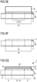
- FIG. 5 is a method for producing an organic optoelectronic device, for example according to FIG. 4 , illustrated.
- the first electrode 11 is applied to the main side 20 of the carrier 2.
- the first electrode 11 is indium tin oxide, ITO for short.
- FIG. 5B is illustrated that on a main surface 6 of the first electrode 11, a photosensitive material 9 is applied and in particular also developed.
- a thickness of the photosensitive material 9 is, for example, about 2 ⁇ m.
- the photosensitive material 9 is preferably a positive resist, English positive resist. That is, by exposure, the photosensitive material 9 is at least partially destroyed or made soluble for certain solvents particularly after development.
- the photosensitive material is, for example, AZ 1518 or OCG 825. Developer for the photosensitive material is, for example, MIF 350.
- the exposure is preferably carried out with unfiltered ultraviolet radiation of a Hg high-pressure lamp or a HgXe high-pressure lamp with a Radiation power of about 4 mW / cm 2 and an exposure time of about 20 s. The exposure takes place only outside a zone 13 of the first electrode 11. In FIG. 5B the exposure is illustrated by arrows.
- the photosensitive material 9 is subsequently removed.
- removing the photosensitive material 9 there is no or no significant material removal with respect to the first electrode 11.
- a thickness of the first electrode 11 is in a direction perpendicular to the main side 20 of the support 2, not affected by the removal of the photosensitive material 9.
- the removal is preferably carried out by ashing with an oxygen plasma and by rinsing with a solvent, for example a glycol ester.
- another photosensitive material 14 is applied and preferably also developed.
- the further light-sensitive material 14 may also be a positive photoresist. Outside a sub-area 15, the other photosensitive material 14 is also exposed, illustrated by arrows.
- the region in which the sub-region 15 and the zone 13 overlap constitutes an overlap region 16.
- the photosensitive material 9 and the further photosensitive material 14 were preferably developed, but not exposed.
- the other photosensitive material outside the subregion 15 is removed.
- the first electrode 11 is removed.
- a structuring of the first electrode 11 takes place by a material removal of a material of the first electrode 11. In particular, at least in places the main side 20 of the carrier 2 is exposed.
- the further photosensitive material 14 is then removed without changing a thickness of the first electrode 11 in the lower region 15.
- the work function of the first electrode 11 is reduced on the main surface 6 of the first electrode 11 in the overlap region 16, as compared to the first electrode 11 outside the overlap region 16.
- the organic optoelectronic component 1 is completed, see FIG. 5G .
- the organic layer sequence 3 with the at least one organic active layer 33 and the second electrode 22 are applied.
- the application can only take place over the first electrode 11 or, unlike in FIG FIG. 5G shown, also made over the entire surface.
- FIG. 5G it is possible that further, in FIG. 5G not shown, for example, for encapsulation of the organic optoelectronic device 1 and in particular the organic layer sequence 3 are applied. Furthermore, it is optionally possible for an antireflection coating to be applied to the radiation passage area 17, for example.
Description
Es wird ein Verfahren zur Herstellung eines organischen optoelektronischen Bauteils angegeben.A process for producing an organic optoelectronic component is specified.
Die Druckschrift
In der Druckschrift
Ein Herstellungsverfahren für ein organisches Display findet sich in der Druckschrift
Die Druckschrift
Diese Aufgabe wird durch ein Verfahren mit den Merkmalen des Anspruchs 1 gelöst.This object is achieved by a method having the features of claim 1.
In einer nicht zur Erfindung gehörenden Abwandlung der Erfindung wird außerdem ein organisches optoelektronisches Bauteil angegeben, welches im Nachfolgenden auch als organisches Bauteil oder als Bauteil angedeutet wird. Gemäß zumindest einer Ausbildung des organischen optoelektronischen Bauteils weist dieses einen Träger auf. Der Träger dient dazu, das Bauteil mechanisch zu stützen. Über den Träger kann das Bauteil also mechanisch stabilisiert sein. Der Träger kann eines der folgenden Materialien umfassen oder aus einem der folgenden Materialien bestehen: Glas, Glasfolie, Quarz, Kunststoff, Kunststofffolie, Metall, Metallfolie, Silizium. Bevorzugt ist das Substrat vollständig oder stellenweise transparent oder transluzent für eine vom Bauteil zu emittierende elektromagnetische Strahlung.In a not belonging to the invention modification of the invention also an organic optoelectronic device is given, which is also indicated below as an organic component or as a component. According to at least one embodiment of the organic optoelectronic component, this has a carrier. The carrier serves to mechanically support the component. About the carrier, the component can therefore be mechanically stabilized. The support may comprise any of the following materials or be made of any of the following materials: glass, glass film, quartz, plastic, plastic film, metal, metal foil, silicon. Preferably, the substrate is completely or partially transparent or translucent for an electromagnetic radiation to be emitted by the component.
Gemäß zumindest einer Ausbildung des Bauteils ist an dem Träger eine erste Elektrode angebracht. Die erste Elektrode kann in direktem, unmittelbarem Kontakt zum Träger stehen. Ebenso ist es möglich, dass zwischen dem Träger und der ersten Elektrode stellenweise oder ganzflächig wenigstens eine Zwischenschicht angebracht ist. Über die Zwischenschicht kann eine Oberflächeneigenschaft des Trägers an die erste Elektrode angepasst sein. Beispielsweise dient die Zwischenschicht zu einer Haftvermittlung zwischen dem Träger und der ersten Elektrode. Auch kann über die Zwischenschicht eine Rauheit einer Oberfläche des Trägers vermindert sein. Ist eine Zwischenschicht vorhanden, so ist diese bevorzugt transparent oder transluzent bezüglich der vom Bauteil zu emittierenden Strahlung gestaltet.According to at least one embodiment of the component, a first electrode is attached to the carrier. The first electrode may be in direct, direct contact with the carrier. Likewise, it is possible that at least one intermediate layer is applied in places or over the entire surface between the carrier and the first electrode. A surface property of the carrier can be adapted to the first electrode via the intermediate layer. For example, the intermediate layer serves for an adhesion mediation between the carrier and the first electrode. Also, a roughness of a surface of the carrier may be reduced via the intermediate layer. If an intermediate layer is present, it is preferably transparent or translucent with respect to the radiation to be emitted by the component.
Gemäß zumindest einer Ausbildung des Bauteils ist die erste Elektrode strahlungsdurchlässig, bevorzugt transparent für die vom Bauteil zu emittierende Strahlung gestaltet. Zum Beispiel ist die erste Elektrode als Anode ausgeführt. Die erste Elektrode dient dann als Löcher-Injizierendes Material. Die erste Elektrode besteht beispielsweise aus einem transparenten leitfähigen Oxid. Geeignete Materialien sind unter anderem Zinkoxid, Zinnoxid, Cadmiumoxid, Titanoxid, Indiumoxid, Indiumzinkoxid oder Indiumzinnoxid. Das Material der ersten Elektrode kann Dotierstoffe aufweisen und zumindest stellenweise p-dotiert oder n-dotiert sein.According to at least one embodiment of the component, the first electrode is permeable to radiation, preferably transparent to the radiation to be emitted by the component. For example, the first electrode is designed as an anode. The first electrode then serves as a hole-injecting material. The first electrode consists for example of a transparent conductive oxide. Suitable materials are including zinc oxide, tin oxide, cadmium oxide, titanium oxide, indium oxide, indium zinc oxide or indium tin oxide. The material of the first electrode may have dopants and be at least locally p-doped or n-doped.
Gemäß zumindest einer Ausbildung des Bauteils ist an einer dem Träger abgewandten Hauptseite der ersten Elektrode eine organische Schichtenfolge aufgebracht. Die organische Schichtenfolge umfasst mindestens eine organische aktive Schicht. Die aktive Schicht ist dazu ausgestaltet, im Betrieb des Bauteils die zu emittierende elektromagnetische Strahlung zu erzeugen. Eine Wellenlänge der Strahlung liegt im Spektralbereich zwischen 200 nm und 3000 nm, bevorzugt zwischen 350 nm und 850 nm. Insbesondere wird im Betrieb in der aktiven Schicht sichtbare Strahlung erzeugt.In accordance with at least one embodiment of the component, an organic layer sequence is applied to a main side of the first electrode facing away from the carrier. The organic layer sequence comprises at least one organic active layer. The active layer is designed to generate the electromagnetic radiation to be emitted during operation of the component. A wavelength of the radiation is in the spectral range between 200 nm and 3000 nm, preferably between 350 nm and 850 nm. In particular, visible radiation is generated during operation in the active layer.
Gemäß zumindest einer Ausbildung des Bauteils weist die organische Schichtenfolge neben der mindestens einen organischen aktiven Schicht zumindest eine Ladungsträgertransportschicht und/oder eine Ladungsträgerinjektionsschicht und/oder eine Ladungsträgerstoppschicht auf.In accordance with at least one embodiment of the component, the organic layer sequence has, in addition to the at least one organic active layer, at least one charge carrier transport layer and / or one charge carrier injection layer and / or one charge carrier stop layer.
Gemäß zumindest einer Ausbildung des Bauteils umfasst die organische aktive Schicht zumindest ein organisches Polymer, ein organisches Oligomer, ein organisches Monomer, organische kleine nicht-polymere Moleküle oder eine Kombination hieraus.According to at least one embodiment of the component, the organic active layer comprises at least one organic polymer, an organic oligomer, an organic monomer, organic small non-polymeric molecules, or a combination thereof.
Gemäß zumindest einer Ausbildung des Bauteils ist an einer dem Träger abgewandten Seite der organischen Schichtenfolge eine zweite Elektrode aufgebracht. Die organische Schichtenfolge befindet sich also zwischen der ersten Elektrode und der zweiten Elektrode. Zum Beispiel ist die zweite Elektrode als Kathode ausgeführt. Insbesondere umfasst die zweite Elektrode eines der folgenden Materialien oder besteht aus einem solchen Material: Aluminium, Barium, Indium, Silber, Gold, Magnesium, Kalzium, Lithium, Stahl. Bevorzugt ist die zweite Elektrode undurchlässig und/oder reflektierend für die in der organischen Schichtenfolge erzeugte Strahlung ausgestaltet. Es ist möglich, dass die zweite Elektrode, neben dem Träger, das Bauteil mechanisch stabilisiert.In accordance with at least one embodiment of the component, a second electrode is applied to a side of the organic layer sequence facing away from the carrier. The organic layer sequence is thus located between the first electrode and the second electrode. For example, the second electrode designed as a cathode. In particular, the second electrode comprises or consists of one of the following materials: aluminum, barium, indium, silver, gold, magnesium, calcium, lithium, steel. The second electrode is preferably impermeable and / or reflective for the radiation generated in the organic layer sequence. It is possible that the second electrode, in addition to the carrier, mechanically stabilizes the component.
Gemäß zumindest einer Ausbildung des Bauteils weist dieses eine Strahlungsdurchtrittsfläche auf. Die Strahlungsdurchtrittsfläche kann eine Begrenzungsfläche des Bauteils sein, durch das die in der aktiven Schicht erzeugte Strahlung oder ein Teil oder ein Großteil dieser Strahlung das Bauteil verlässt. Beispielsweise ist die Strahlungsdurchtrittsfläche durch eine der organischen Schichtenfolge abgewandte Hauptseite des Trägers gebildet. Die Strahlungsdurchtrittsfläche kann auch durch eine beispielsweise antireflektierend wirkende Beschichtung auf dieser Hauptseite des Trägers realisiert sein.According to at least one embodiment of the component, the latter has a radiation passage area. The radiation passage area may be a boundary surface of the component, through which the radiation generated in the active layer or a part or a large part of this radiation leaves the component. By way of example, the radiation passage area is formed by a main side of the carrier facing away from the organic layer sequence. The radiation passage area can also be realized by an example antireflective coating on this main side of the carrier.
Gemäß zumindest einer Ausbildung des organischen Bauteils sind in einer lateralen Richtung mindestens ein Dunkelbereich und mindestens ein Hellbereich ausgebildet. Lateral bedeutet insbesondere entlang zumindest einer Haupterstreckungsrichtung des organischen Bauteils. Der Hellbereich ist hierbei ein Bereich der Strahlungsdurchtrittsfläche des Bauteils, in dem pro Flächeneinheit eine größere Strahlungsleistung emittiert wird als in dem Dunkelbereich. Insbesondere in Draufsicht auf das Bauteil erscheint also im Betrieb des Bauteils der Hellbereich heller als der Dunkelbereich. Bevorzugt weist das Bauteil mehrere Hellbereiche und mehrere Dunkelbereich auf. Die Hellbereiche und die Dunkelbereiche sind hierbei jeweils zusammenhängende Gebiete der Strahlungsdurchtrittsfläche des Bauteils.According to at least one embodiment of the organic component, at least one dark area and at least one bright area are formed in a lateral direction. Lateral means in particular along at least one main extension direction of the organic component. In this case, the bright area is an area of the radiation passage area of the component in which a greater radiation power is emitted per unit area than in the dark area. In particular in a plan view of the component, the bright area appears brighter than the dark area during operation of the component. This preferably has Component several light areas and several dark area on. The light areas and the dark areas are in each case contiguous areas of the radiation passage area of the component.
Gemäß zumindest einer Ausbildung des Bauteils sind sowohl in dem mindestens einen Dunkelbereich als auch in dem mindestens einen Hellbereich vollständig oder stellenweise die erste und die zweite Elektrode sowie die organische Schichtenfolge an dem Träger aufgebracht. Mit anderen Worten weisen dann sowohl der Hellbereich als auch der Dunkelbereich bezüglich der Elektroden und der organischen Schichtenfolge dieselben Komponenten auf. Beispielsweise ist die zweite Elektrode und die organische Schichtenfolge sowohl in dem Hellbereich als auch in dem Dunkelbereich, im Rahmen der Herstellungstoleranzen, identisch gefertigt. Beispielsweise ist ebenso die erste Elektrode eine sich insbesondere durchgängig über den Dunkelbereich und den Hellbereich erstreckende Schicht mit einer bevorzugt, im Rahmen der Herstellungstoleranzen, konstanten Dicke. Das heißt, die Strukturierung der Strahlungsdurchtrittsfläche in Hellbereiche und Dunkelbereiche ist nicht durch eine Formgebung oder geometrische Ausgestaltung der ersten Elektrode, der zweiten Elektrode und der organischen Schichtenfolge erreicht.In accordance with at least one embodiment of the component, the first and the second electrode as well as the organic layer sequence are applied to the carrier completely or in places in the at least one dark area as well as in the at least one bright area. In other words, then both the bright region and the dark region with respect to the electrodes and the organic layer sequence have the same components. By way of example, the second electrode and the organic layer sequence are manufactured identically both in the bright region and in the dark region, within the framework of the manufacturing tolerances. By way of example, the first electrode is likewise a layer extending in particular throughout the dark region and the light region, with a preferably constant thickness within the scope of the manufacturing tolerances. That is, the structuring of the radiation passage area in light areas and dark areas is not achieved by a shaping or geometric configuration of the first electrode, the second electrode and the organic layer sequence.
Gemäß zumindest einer Ausbildung des organischen Bauteils weist dieses eine erste Reflektivität des Dunkelbereichs auf. Zum Beispiel ist die erste Reflektivität eine Reflektivität der Strahlungsdurchtrittsfläche in dem Dunkelbereich. Entsprechend weist das Bauteil eine zweite Reflektivität des Hellbereichs auf, die zum Beispiel eine Reflektivität der Strahlungsdurchtrittsfläche in dem Hellbereich ist.According to at least one embodiment of the organic component, this has a first reflectivity of the dark region. For example, the first reflectivity is a reflectivity of the radiation passage area in the dark area. Accordingly, the component has a second reflectivity of the bright region, which is, for example, a reflectivity of the radiation passage area in the bright region.
Gemäß zumindest einer Ausbildung des organischen Bauteils weicht die erste Reflektivität des Dunkelbereichs von der zweiten Reflektivität des Hellbereichs um höchstens 15 Prozentpunkte, bevorzugt um höchstens 10 Prozentpunkte, insbesondere um höchstens 5 Prozentpunkte voneinander ab. Mit anderen Worten ist eine Reflektivität an der Strahlungsdurchtrittsfläche in dem Hellbereich und eine Reflektivität an der Strahlungsdurchtrittsfläche in dem Dunkelbereich näherungsweise gleich oder, bevorzugt, im Rahmen der Herstellungstoleranzen gleich.According to at least one embodiment of the organic component, the first reflectivity of the dark region deviates from the second reflectivity of the bright region by at most 15 percentage points, preferably by at most 10 percentage points, in particular by at most 5 percentage points from one another. In other words, a reflectivity at the radiation passage area in the bright area and a reflectivity at the radiation passage area in the dark area are approximately equal or, preferably, equal within the manufacturing tolerances.
Die Reflektivität ist zum Beispiel jeweils der Quotient aus einer einfallenden Strahlungsleistung und einer reflektierten, ausfallenden Strahlungsleistung. Zur Bestimmung der Reflektivität wird also beispielsweise die Lichtleistung, die auf die Strahlungsdurchtrittsfläche trifft, gemessen und mit einer von der Strahlungsdurchtrittsfläche reflektierten Lichtleistung verglichen. Beträgt zum Beispiel die erste Reflektivität des Dunkelbereichs 15 %, so liegt die zweite Reflektivität des Hellbereichs bevorzugt zwischen einschließlich 10 % und 20 %.The reflectivity is, for example, in each case the quotient of an incident radiation power and a reflected, outgoing radiation power. For example, to determine the reflectivity, the light output that strikes the radiation passage area is measured and compared with a light output reflected from the radiation passage area. For example, if the first reflectivity of the dark region is 15%, the second reflectivity of the bright region is preferably between 10% and 20% inclusive.
In mindestens einer Ausbildung des organischen optoelektronischen Bauteils umfasst dieses einen Träger sowie eine erste Elektrode, die am Träger angebracht ist. Weiterhin beinhaltet das Bauteil wenigstens eine organische Schichtenfolge mit zumindest einer organischen aktiven Schicht. Weiterhin weist das Bauteil eine zweite Elektrode auf, so dass sich die organische Schichtenfolge zwischen der ersten Elektrode und der zweiten Elektrode befindet. In einer lateralen Richtung sind mindestens ein Dunkelbereich und mindestens ein Hellbereich gebildet. Sowohl in dem Dunkelbereich als auch in dem Hellbereich ist stellenweise oder ganzflächig sowohl die erste Elektrode als auch die zweite Elektrode als auch die organische Schichtenfolge an dem Träger aufgebracht. Eine erste Reflektivität des Dunkelbereichs unterscheidet sich von einer zweiten Reflektivität des Hellbereichs um höchstens 15 Prozentpunkte.In at least one embodiment of the organic optoelectronic component, this comprises a carrier and a first electrode which is attached to the carrier. Furthermore, the component contains at least one organic layer sequence with at least one organic active layer. Furthermore, the component has a second electrode, so that the organic layer sequence is located between the first electrode and the second electrode. In a lateral direction, at least one dark area and at least one bright area are formed. Both in the Dark area as well as in the bright area is applied in places or over the entire surface both the first electrode and the second electrode and the organic layer sequence on the support. A first reflectivity of the dark area differs from a second reflectivity of the bright area by at most 15 percentage points.
Durch den mindestens einen Hellbereich und den mindestens einen Dunkelbereich kann ein Muster und/oder eine Beschriftung und/oder ein Symbol im Betrieb des Bauteils dargestellt werden. Die Hellbereiche bilden helle, leuchtende Bereiche etwa des Musters. Über die nicht oder schwächer leuchtenden Dunkelbereiche ist ein Kontrast zu den Hellbereichen gebildet. Dadurch, dass die erste Reflektivität des Dunkelbereichs und die zweite Reflektivität des Hellbereichs näherungsweise gleich sind, ist es möglich, dass etwa das Muster, das im Betrieb des Bauteils dargestellt wird, außerhalb des Betriebs des Bauteils nicht sichtbar ist. Mit anderen Worten kann, mit bloßem Auge von außen auf das Bauteil gesehen, insbesondere die Strahlungsdurchtrittsfläche des Bauteils homogen und unstrukturiert wirken, wenn das Bauteil nicht betrieben wird. Das heißt, außerhalb des Betriebs des Bauteils ist das Muster von einem Betrachter nicht erkennbar.By the at least one bright area and the at least one dark area, a pattern and / or a label and / or a symbol in the operation of the component can be displayed. The bright areas form bright, luminous areas about the pattern. There is a contrast to the bright areas over the darker or darker dark areas. Because the first reflectivity of the dark area and the second reflectivity of the bright area are approximately the same, it is possible that, for example, the pattern that is displayed during operation of the component is not visible outside the operation of the component. In other words, viewed from the outside with respect to the component with the naked eye, in particular the radiation passage area of the component can be homogeneous and unstructured, if the component is not operated. That is, outside the operation of the component, the pattern is not recognizable by a viewer.
Gemäß zumindest einer Ausbildung des Bauteils ist in dem mindestens einen Dunkelbereich an einer dem Träger abgewandten Hauptfläche der ersten Elektrode eine Monoschicht mit selbstorganisierenden Molekülen aufgebracht. Die Monoschicht ist insbesondere nur in dem Dunkelbereich aufgebracht, sodass der Hellbereich frei ist von der Monoschicht. Bevorzugt ist der gesamte Dunkelbereich von der Monoschicht bedeckt. Mit anderen Worten können Dunkelbereiche ausschließlich dort sein, wo an der organischen Schichtenfolge, insbesondere in einer Richtung senkrecht zur Hauptfläche der ersten Elektrode, die Monoschicht erzeugt ist. Monoschicht bedeutet bevorzugt, dass eine Schichthöhe der Moleküle auf der Hauptseite nur genau ein Molekül beträgt. Es liegen in der Monoschicht demnach bevorzugt keine gleichen Moleküle übereinander.In accordance with at least one embodiment of the component, a monolayer with self-organizing molecules is applied in the at least one dark region on a main surface of the first electrode facing away from the carrier. In particular, the monolayer is applied only in the dark area, so that the bright area is free of the monolayer. Preferably, the entire dark area is covered by the monolayer. In other words, dark areas can be exclusively where, at the organic layer sequence, in particular in a direction perpendicular to the main surface of the first electrode, the monolayer is generated. Monolayer preferably means that a layer height of the molecules on the main side is only exactly one molecule. Accordingly, in the monolayer, preferably no identical molecules are superimposed.
Die Monoschicht befindet sich also zwischen der ersten Elektrode und der organischen Schichtenfolge. Die Monoschicht ist beispielsweise über ein Druckverfahren auf die erste Elektrode aufbringbar. Eine erzielbare Strukturgröße der Monoschicht, in einer lateralen Richtung, beträgt beispielsweise 100 µm, insbesondere 25 µm. Bevorzugt ist die Strukturgröße nur begrenzt durch eine Ortsauflösung eines zum Beispiel verwendeten Druckverfahrens beim Erzeugen der Monoschicht. Mit anderen Worten können sehr feine Muster der Monoschicht erzeugt sein.The monolayer is thus located between the first electrode and the organic layer sequence. The monolayer can be applied, for example, to the first electrode via a printing process. An achievable structure size of the monolayer, in a lateral direction, is for example 100 μm, in particular 25 μm. Preferably, the structure size is limited only by a spatial resolution of a printing process used for example when producing the monolayer. In other words, very fine patterns of the monolayer can be generated.
Gemäß zumindest einer Ausbildung des organischen Bauteils ist die Monoschicht farblos gestaltet. Mit anderen Worten ist ein Absorptionskoeffizient und/oder ein Reflexionskoeffizient der Monoschicht im sichtbaren Spektralbereich näherungsweise nicht von der Wellenlänge abhängig. Beispielsweise ist der Absorptionskoeffizient und/oder der Reflexionskoeffizient im Spektralbereich zwischen 470 nm und 650 nm bis auf eine Abweichung von 10 Prozentpunkten, insbesondere bis auf eine Abweichung von 3 Prozentpunkten konstant. Zum Beispiel liegt der Absoptionskoeffizient zwischen einschließlich 0 % und 10 %, insbesondere zwischen einschließlich 0,01 % und 3 %.According to at least one embodiment of the organic component, the monolayer is colorless. In other words, an absorption coefficient and / or a reflection coefficient of the monolayer in the visible spectral range is approximately not dependent on the wavelength. For example, the absorption coefficient and / or the reflection coefficient in the spectral range between 470 nm and 650 nm is constant except for a deviation of 10 percentage points, in particular to a deviation of 3 percentage points. For example, the absorbency coefficient is between 0% and 10%, especially between 0.01% and 3% inclusive.
Gemäß zumindest einer Ausbildung des organischen Bauteils ist die Monoschicht elektrisch isolierend. In einer Richtung senkrecht zur ersten Elektrode erfolgt also durch die Monoschicht im Betrieb des Bauteils kein Stromfluss hindurch. Weist die organische Schichtenfolge eine vernachlässigbare elektrische Querleitfähigkeit auf, so wird Strahlung in der organischen Schichtenfolge nur in solchen Bereichen erzeugt, in denen keine Monoschicht aufgebracht ist. Bevorzugt weist die Monoschicht eine Durchbruchspannung von mindestens 1 MV/cm auf, insbesondere von mindestens 30 MV/cm, in einer Richtung senkrecht zur ersten Elektrode.According to at least one embodiment of the organic component, the monolayer is electrically insulating. In one direction perpendicular to the first electrode is thus carried by the monolayer during operation of the component no current flow therethrough. If the organic layer sequence has a negligible electrical transverse conductivity, then radiation in the organic layer sequence is produced only in those areas in which no monolayer is applied. The monolayer preferably has a breakdown voltage of at least 1 MV / cm, in particular of at least 30 MV / cm, in a direction perpendicular to the first electrode.
Gemäß zumindest einer Ausbildung des organischen Bauteils liegt eine Dicke der Monoschicht, in einer Richtung senkrecht zur ersten Elektrode, zwischen einschließlich 0,5 nm und 5,0 nm, insbesondere zwischen einschließlich 1,0 nm und 3,0 nm. Die Monoschicht ist also im Vergleich zu einer Wellenlänge einer in der organischen Schichtenfolge erzeugten Strahlung sehr dünn. Daher wirkt sich die Monoschicht auf die optischen Eigenschaften des Bauteils, insbesondere auf den optischen Brechungsindex, nicht oder nur vernachlässigbar aus.According to at least one embodiment of the organic component, a thickness of the monolayer, in a direction perpendicular to the first electrode, is between 0.5 nm and 5.0 nm, in particular between 1.0 nm and 3.0 nm. The monolayer is therefore very thin compared to a wavelength of radiation generated in the organic layer sequence. Therefore, the monolayer affects the optical properties of the component, in particular the optical refractive index, not or only negligible.
Gemäß zumindest einer Ausbildung des organischen Bauteils ist die Monoschicht mit Molekülen gebildet oder besteht aus solchen Molekülen, die lange aliphatische Ketten aufweisen und eine Phosphatgruppe, Silikatgruppe, Carbonylsäuregruppe, Trichlorsilangruppe oder eine ähnliche Gruppe als Kopfgruppe umfassen. Alternativ oder zusätzlich können die Moleküle der Monoschicht auch große Gruppen mit einem konjugierten Ringsystem, wie Benzol oder Cyclopentan, beinhalten. Beispiele für solche Moleküle sind 2[(trimethyloxysily)ethyl]benzene oder 3-[2-(trimethyloxysily) ethyl] pyridine.According to at least one embodiment of the organic component, the monolayer is formed with molecules or consists of those molecules which have long aliphatic chains and comprise a phosphate group, silicate group, carbonyl acid group, trichlorosilane group or a similar group as a head group. Alternatively or additionally, the molecules of the monolayer may also include large groups having a conjugated ring system, such as benzene or cyclopentane. Examples of such molecules are 2 [(trimethyloxysily) ethyl] benzene or 3- [2- (trimethyloxysily) ethyl] pyridines.
Gemäß zumindest einer Ausbildung des organischen Bauteils weist der Träger an einer der Schichtenfolge zugewandten Seite in dem Dunkelbereich eine Aufrauung auf. Mit anderen Worten ist die der Schichtenfolge zugewandte Seite des Trägers in dem Hellbereich näherungsweise glatt und in dem Dunkelbereich gezielt rau. Die Aufrauung befindet sich also zwischen dem Träger und der ersten Elektrode.According to at least one embodiment of the organic component, the carrier has a roughening on a side facing the layer sequence in the dark region. In other words, the side of the carrier facing the layer sequence is approximately smooth in the bright region and deliberately rough in the dark region. The roughening is thus between the carrier and the first electrode.
Gemäß zumindest einer Ausbildung des organischen Bauteils weist die Strahlungsdurchtrittsfläche, im Rahmen der Herstellungstoleranzen, in dem Hellbereich als auch in dem Dunkelbereich eine gleiche Beschaffenheit auf, beispielsweise im Hinblick auf eine Rauheit. Mit anderen Worten ist insbesondere die der organischen Schichtenfolge abgewandte Seite des Trägers nicht strukturiert.In accordance with at least one embodiment of the organic component, the radiation passage area, in the context of the manufacturing tolerances, in the bright area as well as in the dark area has the same characteristics, for example with regard to roughness. In other words, in particular the side of the carrier facing away from the organic layer sequence is not structured.
Gemäß zumindest einer Ausbildung des organischen Bauteils beträgt eine mittlere Rauheit der Aufrauung zwischen einschließlich 5 nm und 1 pm, insbesondere zwischen einschließlich 20 nm und 500 nm. Die Aufrauung weist also insbesondere eine mittlere Rauheit auf, die kleiner oder gleich einer Wellenlänge der in der organischen Schichtenfolge erzeugten Strahlung liegt.According to at least one embodiment of the organic component, an average roughness of the roughening is between 5 nm and 1 pm, in particular between 20 nm and 500 nm inclusive. The roughening thus has in particular an average roughness which is less than or equal to a wavelength in the organic Layer sequence generated radiation is.
Gemäß zumindest einer Ausbildung des organischen Bauteils weist die Aufrauung und/oder der Dunkelbereich eine laterale Strukturgröße von mindestens 1 mm, insbesondere von mindestens 3 mm, auf. Mit anderen Worten weist die Aufrauung, und somit bevorzugt auch der Dunkelbereich, in einer oder in zwei Richtungen eine Ausdehnung von mindestens den genannten Werten auf. Die Aufrauung kann also flächig ausgeformt sein.According to at least one embodiment of the organic component, the roughening and / or the dark region has a lateral structure size of at least 1 mm, in particular of at least 3 mm. In other words, the roughening, and thus preferably also the dark area, has an extent of at least the stated values in one or in two directions. The roughening can thus be formed flat.
Gemäß zumindest einer Ausbildung des organischen Bauteils ist die Aufrauung des Trägers in dem Dunkelbereich durch rillenartige oder kanalartige Strukturen gebildet, die eine der mittleren Rauheit entsprechende mittlere Tiefe aufweisen. Rillenartig kann bedeuten, dass eine mittlere Länge eine mittlere Breite der Strukturen mindestens um ein Zehnfaches übersteigt.According to at least one embodiment of the organic component, the roughening of the carrier in the dark region is formed by groove-like or channel-like structures which have a mean depth corresponding to the average roughness. Grooved may mean that an average length exceeds a mean width of the structures at least ten times.
Gemäß zumindest einer Ausbildung des organischen Bauteils befindet sich zwischen dem Träger und der ersten Elektrode eine Zwischenschicht. Die Zwischenschicht weist bevorzugt einen Brechungsindex auf, der von dem des Trägers um höchstens 0,1, insbesondere um höchstens 0,05 abweicht. Beträgt der Brechungsindex des Trägers beispielsweise 1,50, so liegt der Brechungsindex der Zwischenschicht bevorzugt zwischen 1,45 und 1,55. Beispielsweise ist die Zwischenschicht eine Oxidschicht, insbesondere eine Siliziumdioxidschicht.According to at least one embodiment of the organic component, an intermediate layer is located between the carrier and the first electrode. The intermediate layer preferably has a refractive index which deviates from that of the carrier by at most 0.1, in particular by at most 0.05. For example, if the refractive index of the carrier is 1.50, the refractive index of the intermediate layer is preferably between 1.45 and 1.55. For example, the intermediate layer is an oxide layer, in particular a silicon dioxide layer.
Gemäß zumindest einer Ausbildung des organischen Bauteils beträgt eine Dicke der Zwischenschicht, in einer Richtung senkrecht zur ersten Elektrode, zwischen einschließlich 10 nm und 200 nm, insbesondere zwischen einschließlich 15 nm und 40 nm. Ist die Zwischenschicht über der Aufrauung angebracht, so ist eine dem Träger abgewandte Seite der Zwischenschicht bevorzugt glatter als der Träger im Bereich der Aufrauung. Die mittlere Dicke der Zwischenschicht kann im Bereich der mittleren Rauheit der Aufrauung des Trägers liegen.According to at least one embodiment of the organic component, a thickness of the intermediate layer, in a direction perpendicular to the first electrode, is between 10 nm and 200 nm inclusive, in particular between 15 nm and 40 nm inclusive. If the intermediate layer is applied over the roughening, then a Carrier side facing away from the intermediate layer preferably smoother than the carrier in the roughening. The average thickness of the intermediate layer may be in the range of the average roughness of the roughening of the carrier.
Gemäß zumindest einer Ausbildung des organischen Bauteils beträgt eine mittlere Strahlungsleistung pro Flächeneinheit des mindestens einen Dunkelbereichs höchstens 60 %, insbesondere höchstens 45 % der mittleren Strahlungsleistung pro Flächeneinheit des mindestens einen Hellbereichs. Beispielsweise wird in dem Dunkelbereich näherungsweise keine Strahlungsleistung emittiert. Ebenso ist es möglich, dass die Strahlungsleistung pro Flächeninhalt des Dunkelbereichs zwischen einschließlich 1 % und 60 % der des Hellbereichs beträgt, bevorzugt zwischen einschließlich 2 % und 45 %, insbesondere zwischen einschließlich 4 % und 30 %.According to at least one embodiment of the organic component, an average radiation power per unit area of the at least one dark area is at most 60%, in particular at most 45%, of the mean radiation power per unit area of the at least one bright area. For example, approximately no radiant power is emitted in the dark region. It is also possible that the radiant power per area of the dark area is between 1% and 60% of that of the bright area, preferably between 2% and 45% inclusive, in particular between 4% and 30% inclusive.
Gemäß zumindest einer Ausbildung des organischen Bauteils ist der Träger mit einem Glas, die erste Elektrode mit einem leitfähigen transparenten Oxid und die zweite Elektrode mit einem Metall gestaltet oder bestehen aus den genannten Werkstoffen. Die in der organischen Schichtenfolge erzeugte Strahlung durchläuft also den Träger und wird insbesondere an einer der organischen Schichtenfolge abgewandten Hauptseite des Trägers emittiert.According to at least one embodiment of the organic component, the carrier is designed with a glass, the first electrode with a conductive transparent oxide and the second electrode with a metal or consist of the materials mentioned. The radiation generated in the organic layer sequence thus passes through the carrier and is emitted, in particular, on a main side of the carrier facing away from the organic layer sequence.
Gemäß zumindest einer Ausbildung des organischen Bauteils weist eine Hauptfläche der ersten Elektrode, die dem Träger abgewandt ist, in dem mindestens einen Dunkelbereich eine höhere Austrittsarbeit auf als in dem mindestens einen Hellbereich. Die Austrittsarbeit ist beispielsweise die minimale Energie, die benötigt wird, um einen Ladungsträger wie ein Elektron von einem Punkt innerhalb der ersten Elektrode an einen Punkt außerhalb der Oberfläche der ersten Elektrode zu befördern. Beispielsweise unterscheidet sich die Austrittsarbeit der ersten Elektrode in dem Dunkelbereich von der Austrittsarbeit in dem Hellbereich um mindestens 0,10 eV, bevorzugt um mindestens 0,25 eV, insbesondere um mindestens 0,40 eV. Ein Absolutwert der Austrittsarbeit liegt hierbei bevorzugt zwischen einschließlich 4,0 eV und 5,0 eV, insbesondere bei zirka 4,5 eV. Eine Modifizierung der Austrittsarbeit wird bevorzugt nicht dadurch erreicht, dass eine separate Beschichtung, zum Beispiel mit einer dünnen, insbesondere monolagigen Schicht organischer Moleküle, aufgebracht wird. Mit anderen Worten ist die erste Elektrode dann frei von einer solchen separaten, die Austrittsarbeit beeinflussenden Beschichtung.According to at least one embodiment of the organic component, a main surface of the first electrode facing away from the carrier has a higher work function in the at least one dark region than in the at least one bright region. For example, the work function is the minimum energy required to carry a charge carrier, such as an electron, from a point within the first electrode to a point outside the surface of the first electrode. For example, the work function of the first electrode in the dark region differs from the work function in the light region by at least 0.10 eV, preferably by at least 0.25 eV, in particular by at least 0.40 eV. An absolute value of the work function here is preferably between 4.0 eV and 5.0 eV, in particular at about 4.5 eV. A modification of the work function is preferably not achieved in that a separate coating is applied, for example with a thin, in particular monolayer, layer of organic molecules. In other words, the first electrode is then free of such a separate, the work function affecting coating.
Beispielsweise kann mittels des erfindungsgemäßen Verfahrens ein organisches optoelektronisches Bauteil hergestellt werden, wie es in Verbindung mit einer oder mehrerer der oben genannten Ausbildungen beschrieben ist. Merkmale des organischen optoelektronischen Bauteils sind daher auch für das hier beschriebene Verfahren offenbart und umgekehrt.For example, by means of the method according to the invention, an organic optoelectronic component can be produced, as described in connection with one or more of the abovementioned embodiments. Features of the organic optoelectronic component are therefore also disclosed for the method described here and vice versa.
In mindestens einer Ausführungsform des Verfahrens umfasst dieses die folgenden Schritte:
- Bereitstellen eines Trägers mit einer ersten Elektrode,
- Aufbringen und, außerhalb einer Zone, Belichten eines lichtempfindlichen Materials an der ersten Elektrode,
- Entfernen des lichtempfindlichen Materials, wobei eine Dicke der ersten Elektrode im Rahmen der Herstellungstoleranzen unverändert bleibt,
- Aufbringen und, außerhalb eines Unterbereichs, Belichten eines weiteren lichtempfindlichen Materials an der ersten Elektrode,
- Entfernen des weiteren lichtempfindlichen Materials, und
- Erzeugen einer organischen Schichtenfolge mit zumindest einer organischen aktiven Schicht und einer zweiten Elektrode zumindest an der ersten Elektrode. Hierbei ist eine Austrittsarbeit an einer dem Träger abgewandten Hauptfläche der ersten Elektrode in mindestens einen Überlappbereich, in dem die Zone und der Unterbereich überlappen, im Vergleich zu übrigen Bereichen der ersten Elektrode herabgesetzt.
- Providing a carrier with a first electrode,
- Applying and, outside a zone, exposing a photosensitive material to the first electrode,
- Removing the photosensitive material, wherein a thickness of the first electrode remains unchanged within the manufacturing tolerances,
- Applying and, outside a sub-region, exposing a further photosensitive material to the first electrode,
- Removing the further photosensitive material, and
- Generating an organic layer sequence with at least one organic active layer and a second electrode at least at the first electrode. In this case, a work function on a main surface of the first electrode facing away from the carrier is reduced in at least one overlap region, in which the zone and the subregion overlap, in comparison to other regions of the first electrode.
Mit anderen Worten wird in einem Verfahrensschritt etwa ein Fotolack auf der ersten Elektrode aufgebracht, und der Fotolack wird mindestens stellenweise belichtet. Anschließend wird der Fotolack beispielsweise nach einem Entwickeln entfernt, wobei die erste Elektrode nicht strukturiert wird. In einem anderen Schritt des Verfahrens wird ein weiteres lichtempfindliches Material, etwa ein Fotolack, auf der ersten Elektrode aufgebracht, belichtet und insbesondere auch entwickelt, und anschließend wiederum entfernt. Der mindestens eine Hellbereich ist dann durch einen solchen Bereich der ersten Elektrode gebildet, in dem zweifach lichtempfindliches Material aufgebracht und wieder entfernt wurde und der keiner Belichtung des lichtempfindlichen Materials ausgesetzt war. Derzeit wird angenommen, dass über das zweifache Auftragen, das zweifache Entfernen und bevorzugt auch das zweifache Entwickeln des lichtempfindlichen, unbelichteten Materials die Austrittsarbeit der ersten Elektrode herabsetzbar ist. Die herabgesetzte Austrittsarbeit führt wiederum dazu, dass der so behandelte Bereich im Betrieb des hergestellten Bauteils heller erscheint.In other words, in one method step, for example, a photoresist is applied to the first electrode, and the photoresist is exposed at least in places. Subsequently, the photoresist is removed, for example, after development, wherein the first electrode is not patterned. In another step of the method, another photosensitive material, such as a photoresist, is applied to the first electrode, exposed and, in particular, developed, and then removed again. The at least one bright region is then formed by such a region of the first electrode in which two-fold photosensitive material was applied and removed again and which was not exposed to any exposure of the photosensitive material. At present, it is believed that over twice the application, the double removal, and preferably also the twofold development of the photosensitive, unexposed material, the work function of the first electrode is degradable. The reduced work function in turn causes the thus treated area appears brighter in the operation of the manufactured component.
Gemäß zumindest einer Ausführungsform des Verfahrens ist die erste Elektrode mit Indiumzinnoxid gestaltet oder besteht aus Indiumzinnoxid. Weiterhin wird das lichtempfindliche Material und/oder das weitere lichtempfindliche Material über ein Veraschen mit einem O2-Plasma und/oder über Spülen mit einem Lösungsmittel entfernt.According to at least one embodiment of the method, the first electrode is designed with indium tin oxide or consists of indium tin oxide. Further, the photosensitive material and / or the other photosensitive material is removed by ashing with an O 2 plasma and / or by rinsing with a solvent.
Gemäß zumindest einer Ausführungsform des Verfahrens wird zwischen dem Schritt des Belichtens des weiteren lichtempfindlichen Materials und dem Schritt des Entfernens des weiteren lichtempfindlichen Materials in einem zusätzlichen Verfahrensschritt außerhalb des Unterbereichs, in welchem das weitere lichtempfindliche Material nicht belichtet wurde, ein Material der ersten Elektrode vollständig oder teilweise entfernt. Mit anderen Worten wird die erste Elektrode über eine durch das weitere lichtempfindliche Material gebildete Maske strukturiert, wobei das Strukturieren durch Materialwegnahme der ersten Elektrode außerhalb des Unterbereichs, beispielsweise durch Wegätzen, erfolgt.According to at least one embodiment of the method, a material of the first electrode is completely or between the step of exposing the further photosensitive material and the step of removing the further photosensitive material in an additional process step outside the sub-area in which the further photosensitive material has not been exposed partially removed. In other words, the first electrode is patterned via a mask formed by the further photosensitive material, wherein structuring takes place by removal of material from the first electrode outside the subregion, for example by etching away.
Gemäß zumindest einer Ausführungsform des Verfahrens wird durch den Überlappbereich, in dem der Unterbereich und die Zone überlappen, mindestens ein Hellbereich gebildet. Der Hellbereich stellt also zumindest einen Bereich der ersten Elektrode dar,
- in dem auf der ersten Elektrode zweifach ein lichtempfindliches Material aufgebracht wurde,
- der nicht belichtet wurde,
- in dem die lichtempfindlichen Materialien jeweils wieder entfernt wurden, und
- in dem bevorzugt die lichtempfindlichen Materialien jeweils auch entwickelt wurden.
- in which a photosensitive material was applied twice on the first electrode,
- that was not exposed,
- in which the photosensitive materials were removed again, and
- in which preferably the photosensitive materials were also developed.
Gemäß zumindest einer Ausführungsform des Verfahrens wird in einen verbleibenden, nicht zum Hellbereich gehörenden Bereich des Unterbereichs mindestens ein Dunkelbereich geformt. Der mindestens eine Hellbereich und der mindestens eine Dunkelbereich unterscheiden sich also nicht in einer Dicke oder Materialzusammensetzung der ersten Elektrode, sondern lediglich durch eine Austrittsarbeit an einer dem Träger abgewandten Hauptseite der ersten Elektrode.In accordance with at least one embodiment of the method, at least one dark area is formed in a remaining area of the subarea that does not belong to the bright area. The at least one bright area and the at least one dark area therefore do not differ in thickness or material composition of the first electrode, but only by a work function on a side facing away from the carrier main side of the first electrode.
Gemäß zumindest einer Ausführungsform des Verfahrens wird die erste Elektrode aus Indiumzinnoxid, kurz ITO, geformt oder besteht aus ITO. Das Belichten des lichtempfindlichen Materials und des weiteren lichtempfindlichen Materials erfolgt mit Wellenlängen zwischen einschließlich 240 nm und 380 nm. Als lichtempfindliches Material wird jeweils ein positiver Fotolack verwendet. Insbesondere in dem Hellbereich erfolgt ein Entwickeln sowohl des lichtempfindlichen Materials als auch des weiteren lichtempfindlichen Materials.In accordance with at least one embodiment of the method, the first electrode is formed from indium tin oxide, ITO for short, or consists of ITO. The photosensitive material and the other photosensitive material are exposed to wavelengths of between 240 nm and 380 nm inclusive. The photosensitive material used is a positive photoresist. In particular, in the bright region, development of both the photosensitive material and the other photosensitive material takes place.
Gemäß zumindest einer Ausführungsform des Verfahrens werden die lichtempfindlichen Materialien vollständig entfernt. Mit anderen Worten ist das fertige, organische Bauteil dann frei von den lichtempfindlichen Materialien.In accordance with at least one embodiment of the method, the photosensitive materials are completely removed. In other words, the finished, organic component is then free of the photosensitive materials.
Einige Anwendungsbereiche, in denen hier beschriebene organische Bauteile Verwendung finden können, sind etwa die Hinterleuchtungen von Displays oder Anzeigeeinrichtungen. Weiterhin können hier beschriebene optoelektronische Bauteile in Beleuchtungseinrichtungen zu Projektionszwecken, in Scheinwerfern oder Lichtstrahlern oder bei der Allgemeinbeleuchtung eingesetzt werden.Some applications in which organic components described here can be used are, for example, the backlighting of displays or display devices. Furthermore, optoelectronic components described here can be used in illumination devices for projection purposes, in headlamps or light emitters or in general lighting.
Nachfolgend wird ein Bauteil sowie ein hier beschriebenes Verfahren unter Bezugnahme auf die Zeichnung anhand von Ausbildungen und Ausführungsbeispielen näher erläutert. Gleiche Bezugszeichen geben dabei gleiche Elemente in den einzelnen Figuren an. Es sind dabei jedoch keine maßstäblichen Bezüge dargestellt, vielmehr können einzelne Elemente zum besseren Verständnis übertrieben groß dargestellt sein.Hereinafter, a component and a method described herein with reference to the drawings with reference to embodiments and embodiments will be explained in more detail. The same reference numerals indicate the same elements in the individual figures. However, they are not scale relationships shown, but individual elements may be exaggerated to better understand.
Es zeigen:
- Figur 1
- eine schematische Schnittdarstellung einer Ausbildung eines organischen optoelektronischen Bauteils,
Figur 2- eine schematische Illustration einer Bestimmung einer Reflektivität von Hellbereichen und Dunkelbereichen,
- Figuren 3 und 4
- schematische Schnittdarstellungen von weiteren Ausbildungen von organischen Bauteilen, und
Figur 5- eine schematische Darstellung eines Ausführungsbeispiels eines hier beschriebenen Verfahrens zur Herstellung einer Ausbildung eines organischen optoelektronischen Bauteils.
- FIG. 1
- 1 is a schematic sectional view of a construction of an organic optoelectronic device,
- FIG. 2
- a schematic illustration of a determination of a reflectivity of bright areas and dark areas,
- FIGS. 3 and 4
- schematic sectional views of further embodiments of organic components, and
- FIG. 5
- a schematic representation of an embodiment of a method described herein for producing a formation of an organic optoelectronic device.
In
An einer dem Träger 2 abgewandten Hauptfläche 6 der ersten Elektrode 11 ist eine organische Schichtenfolge 3 mit einer organischen aktiven Schicht 33 aufgebracht. An einer dem Träger 2 abgewandten Seite der organischen Schichtenfolge 3 befindet sich eine zweite Elektrode 22. Im Betrieb des organischen optoelektronischen Bauteils 1 wird also die organische Schichtenfolge 3 über die erste Elektrode 11 und die zweite Elektrode 22 bestromt. In der organischen aktiven Schicht 33 wird im Betrieb des organischen optoelektronischen Bauteils 1 eine elektromagnetische Strahlung, bevorzugt im sichtbaren oder nahen ultravioletten Spektralbereich, generiert.An organic layer sequence 3 with an organic active layer 33 is applied to a
Der Träger 2 ist zum Beispiel mit Glas oder mit einer Glasfolie gestaltet. Die erste Elektrode 11 besteht zum Beispiel aus Indiumzinnoxid oder Indiumzinkoxid. Eine Dicke des Trägers 2, in einer Richtung senkrecht zur Hauptseite 20 des Trägers 2, beträgt beispielsweise zwischen einschließlich 200 µm und 2 mm. Eine Dicke der ersten Elektrode 11 beträgt zum Beispiel zwischen einschließlich 50 nm und 200 nm, insbesondere zirka 120 nm. Ein Brechungsindex eines Materials der ersten Elektrode 11 liegt insbesondere zwischen einschließlich 1,7 und 1,8. Ein Brechungsindex eines Materials des Trägers 2 beträgt zwischen etwa 1,45 und 1,55. Die organische Schichtenfolge 3 weist eine Dicke in der Größenordnung von 100 nm auf. Eine Dicke der zweiten Elektrode 22, die zum Beispiel durch ein aufgedampftes Metall oder durch eine Stahlfolie gebildet ist, liegt bevorzugt im Bereich von 20 nm bis 500 µm.The
Auf der Hauptfläche 6 der ersten Elektrode 11 ist stellenweise eine Monoschicht 7 aufgetragen. Die Monoschicht 7 besteht aus selbstorganisierenden Molekülen. Beispielsweise ist die Monoschicht 7 mittels eines Druckverfahrens auf der Hauptfläche 6 aufgebracht. Eine Dicke der Monoschicht 7, in eine Richtung senkrecht zur Hauptfläche 6 der ersten Elektrode 11, beträgt insbesondere zwischen 0,5 nm und 5,0 nm. Die Dicke der Monoschicht 7 ist also bevorzugt um ein Vielfaches kleiner als die Dicke der organischen Schichtenfolge 3. Die Monoschicht 7 ist elektrisch isolierend und optisch transparent.On the
Da die organische Schichtenfolge 3 nur eine vernachlässigbare elektrische Querleitfähigkeit in einer Richtung parallel zur Hauptfläche 6 der ersten Elektrode 11 aufweist, erfolgt eine Bestromung der organischen aktiven Schicht 33 nur in solchen Bereichen, in denen keine Monoschicht 7 auf der ersten Elektrode 11 aufgebracht ist. Diese Bereiche, in denen die Monoschicht 7 aufgebracht ist, stellen also Dunkelbereiche 4 dar. Die Bereiche, in denen keine Monoschicht 7 aufgebracht ist, bilden Hellbereiche 5. Im Betrieb des organischen optoelektronischen Bauteils 1 erscheinen die Dunkelbereiche 4 also deutlich dunkler als die Hellbereiche 5. Näherungsweise wird in den Dunkelbereichen 4 in der organischen aktiven Schicht 33 keine elektromagnetische Strahlung im Betrieb des organischen optoelektronischen Bauteils 1 erzeugt.Since the organic layer sequence 3 has only a negligible electrical transverse conductivity in a direction parallel to the
Bei dem organischen optoelektronischen Bauteil 1 unterscheiden sich also die erste Elektrode 11, die organische Schichtenfolge 3 sowie die zweite Elektrode 22 bezüglich ihrer Ausgestaltung in den Dunkelbereichen 4 und in den Hellbereichen 5 nicht voneinander. Insbesondere dadurch, dass die erste Elektrode 11 im Wesentlichen die gesamte Hauptseite 20 des Trägers 2 bedeckt, ist außerhalb des Betriebs des organischen optoelektronischen Bauteils 1 ein durch die Monoschicht 7 gebildetes Muster der Hellbereiche 5 und der Dunkelbereiche 4 nicht erkennbar. Da die erste Elektrode 11 einen von dem Träger 2 deutlich unterschiedlichen Brechungsindex und somit ein unterschiedliches Reflexionsverhalten aufweist, wäre im Fall einer ersten Elektrode 11, die beispielsweise in den Dunkelbereichen 4 abgetragen wäre, das durch die Dunkelbereiche 4 und durch die Hellbereiche 5 gebildete Muster außerhalb des Betriebs des organischen optoelektronischen Bauteils 1 erkennbar.In the case of the organic optoelectronic component 1, therefore, the
Eine in der organischen aktiven Schicht 33 erzeugte Strahlung verlässt das organische optoelektronische Bauteil 1 durch den Träger 2 hindurch. Eine der ersten Elektrode 11 abgewandte Hauptseite des Trägers 2 bildet hierbei eine Strahlungsdurchtrittsfläche 17. Bevorzugt ist die zweite Elektrode 22 bezüglich der in der organischen Schichtenfolge 3 erzeugten Strahlung reflektierend und/oder strahlungsundurchlässig gestaltet.A radiation generated in the organic active layer 33 leaves the organic optoelectronic component 1 through the
Mit anderen Worten sind die Dunkelbereiche 4 und die Hellbereiche 5, außerhalb des Betriebs des organischen optoelektronischen Bauteils 1 und auf die Strahlungsdurchtrittsfläche 17 gesehen, nicht voneinander unterscheidbar. In dem Fall, dass die zweite Elektrode 22 lichtundurchlässig ist, bedeutet dies, dass sich eine erste Reflektivität der Dunkelbereiche 4 von einer zweiten Reflektivität der Hellbereiche 5 näherungsweise nicht unterscheidet.In other words, the
Die erste und die zweite Reflektivität sind in
Beispielsweise weichen die erste und die zweite Reflektivität im sichtbaren Spektralbereich, also insbesondere zwischen 480 nm und 640 nm, sowie in einem Einfallswinkelbereich zwischen einschließlich 0° und 70° nicht oder näherungsweise nicht voneinander ab.For example, the first and the second reflectivity are different in the visible spectral range, ie in particular between 480 nm and 640 nm, and in an angle of incidence range between including 0 ° and 70 ° or not approximately from each other.
Für den Fall, dass das organische optoelektronische Bauteil 1 transparent oder strahlungsdurchlässig ist, können alternativ oder zusätzlich zur ersten Reflektivität und zur zweiten Reflektivität in analoger Weise Transmissionswerte des organischen optoelektronischen Bauteils 1 in den Dunkelbereichen 4 und in den Hellbereichen 5 bestimmt und miteinander verglichen werden. Bevorzugt unterscheiden sich dann die Transmissionswerte in den Dunkelbereichen 4 und in den Hellbereichen 5 sowie bevorzugt auch deren Reflektivitäten nicht oder näherungsweise nicht voneinander. Dass die Dunkelbereiche 4 und die Hellbereiche 5 außerhalb des Betriebs des organischen optoelektronischen Bauteils 1 von außerhalb des Bauteils nicht visuell unterscheidbar sind, liegt also zusammengefasst insbesondere daran, dass die erste Elektrode 11 sowohl die Dunkelbereiche 4 als auch die Hellbereiche 5 überspannt, und daran, dass die Monoschicht 7 die Reflektivität, eine Absorption und/oder die Transmission von Strahlung am oder durch das organische optoelektronische Bauteil 1 hindurch nicht oder nicht signifikant beeinflusst.In the case that the organic optoelectronic component 1 is transparent or radiation-permeable, as an alternative or in addition to the first reflectivity and the second reflectivity, transmission values of the organic optoelectronic component 1 in the
Eine weitere Ausbildung des organischen optoelektronischen Bauteils 1 ist in
In den Dunkelbereichen 4 weist die Hauptseite 20 des Trägers 2 eine Aufrauung 8 auf. Die Aufrauung 8 ist von der Zwischenschicht 12 überdeckt. Eine dem Träger 2 abgewandte Hauptseite der Zwischenschicht 12 ist näherungsweise glatt. Mit anderen Worten kann die Zwischenschicht 12 die Aufrauung 8 des Trägers 2 vollständig oder zum Teil glätten.In the
Die erste Elektrode 11, die zweite Elektrode 22 sowie die organische Schichtenfolge 3 sind also über der Hauptseite 20 des Trägers 2 im Rahmen der Herstellungstoleranzen überall gleich aufgebracht. In lateraler Richtung wird in der gesamten organischen Schichtenfolge 3 eine Strahlung im Betrieb des organischen optoelektronischen Bauteils 1 erzeugt. Über die Aufrauung 8 erfolgt eine Lichtablenkung aus den Dunkelbereichen 4 weg in Richtung zu den Hellbereichen 5. Hierdurch ist eine mittlere Strahlungsleistung pro Fläche, die an der Strahlungsdurchtrittsfläche 17 das organische optoelektronische Bauteil 1 verlässt, in den Dunkelbereichen 4 um beispielsweise 50 % geringer als in den Hellbereichen 5. Durch die Aufrauung 8 ist eine Reflektivität der Strahlungsdurchtrittsfläche und der ersten Elektrode 11 näherungsweise nicht beeinflusst. Außerhalb des Betriebs des organischen optoelektronischen Bauteils 1 sind also die Dunkelbereiche 4 von den Hellbereichen 5, auf die Strahlungsdurchtrittsfläche 17 gesehen, nicht unterscheidbar.The
Eine mittlere Rauheit der Aufrauung 8 liegt beispielsweise zwischen einschließlich 20 nm und 500 nm. Die Aufrauung ist etwa durch Laserbestrahlung der Hauptseite 20 des Trägers 2 oder durch Schleifen der Hauptseite 20 mit einem Schleifmittel mit einer definierten Körnung erzielbar. Die Aufrauung 8 kann bezüglich Haupterstreckungsrichtungen des Trägers 2 isotrop gestaltet sein oder auch zum Beispiel in Form von näherungsweise parallel laufenden Kanälen einer der Rauheit entsprechenden mittleren Tiefe realisiert sein.An average roughness of the
Bei der Ausbildung gemäß
Die Austrittsarbeit an der Hauptfläche 6 der ersten Elektrode 11 in den Hellbereichen 5 sowie der ersten Elektrode 11 in den Dunkelbereichen 4 ist beispielsweise messbar, in dem die zweite Elektrode 22 und die aktive Schichtenfolge von der ersten Elektrode 11 entfernt werden, wobei die Hauptfläche 6 der ersten Elektrode 11 näherungsweise nicht verändert wird. Anschließend ist die Austrittsarbeit lokal etwa über Photoelektronenemissionsspektroskopie messbar.The work function on the
Optional kann auch bei den Ausbildungen gemäß der
In
In einem Verfahrensschritt, siehe
In
Bei dem lichtempfindlichen Material handelt es sich beispielsweise um AZ 1518 oder OCG 825. Als Entwickler, englisch Developer, für das lichtempfindliche Material dient zum Beispiel MIF 350. Das Belichten erfolgt bevorzugt mit ungefilterter ultravioletter Strahlung einer Hg-Hochdrucklampe oder einer HgXe-Hochdrucklampe mit einer Strahlungsleistung von zirka 4 mW/cm2 und einer Belichtungsdauer von zirka 20 s. Die Belichtung erfolgt nur außerhalb einer Zone 13 der ersten Elektrode 11. In
Wie in
Weiterhin wird auf der ersten Elektrode 11, siehe
Die Zone 13 der ersten Elektrode 11, außerhalb der bereits eine Belichtung des lichtempfindlichen Materials 9 erfolgte, ist von dem Unterbereich 15 vollständig oder teilweise umfangen. Der Bereich, in dem der Unterbereich 15 und die Zone 13 überlappen, stellt einen Überlappbereich 16 dar. In dem Überlappbereich 16 wurden also das lichtempfindliche Material 9 und das weitere lichtempfindliche Material 14 bevorzugt jeweils entwickelt, nicht jedoch belichtet. In einem weiteren Verfahrensschritt, siehe
Wie in
Durch das bevorzugt zweimalige Entwickeln und das zweimalige Entfernen des lichtempfindlichen Materials 9 und des weiteren lichtempfindlichen Materials 14 ist an der Hauptfläche 6 der ersten Elektrode 11 in dem Überlappbereich 16 die Austrittsarbeit der ersten Elektrode 11 im Vergleich zur ersten Elektrode 11 außerhalb des Überlappbereichs 16 herabgesetzt.By preferably developing twice and removing twice the
Abschließend wird das organische optoelektronische Bauteil 1 fertig gestellt, siehe
Optional ist es möglich, dass weitere, in
Claims (2)
- A method for producing an organic optoelectronic component (1) with the steps:- provision of a carrier (2) with a first electrode (11),- application of and, outside a zone (13), exposure of a light-sensitive material (9) on the first electrode (11),- removal of the light-sensitive material (9), wherein a thickness of the first electrode (11) remains unchanged,- application of and, outside a sub-region (15), exposure of another light-sensitive material (14) on the first electrode (11),- removal of the other light-sensitive material (14), and- production of an organic layer sequence (3) with at least one organic active layer (33) and a second electrode (22) at least on the first electrode (11),wherein a work function on a major surface (6) of the first electrode (11) remote from the carrier (2) is reduced in at least one overlap region (16), in which the zone (13) and the sub-region (15) overlap, compared with other regions of the first electrode (11), wherein between the step of exposure and the step of removal of the other light-sensitive material (14), a material of the first electrode (11) is removed in a further step outside the sub-region (15),
and wherein due to the overlap region (16) at least one light region (5) is formed,
and wherein at least one dark region (4) is formed by a remaining area of the sub-region (15) not belonging to the light region (5). - The method according to the previous Claim, wherein the first electrode (11) is formed with or from indium tin oxide, the exposure of the light-sensitive material (9) and the other light-sensitive material (14) is carried out at wavelengths between 240 nm and 380 nm inclusively, and a positive photoresist is used as the light-sensitive material (9) and as the other light-sensitive material (14) and both light-sensitive materials are developed in the overlap region (16).
Applications Claiming Priority (3)
| Application Number | Priority Date | Filing Date | Title |
|---|---|---|---|
| DE102009015574 | 2009-03-30 | ||
| DE102009022902.7A DE102009022902B4 (en) | 2009-03-30 | 2009-05-27 | Organic optoelectronic component and method for producing an organic optoelectronic component |
| PCT/EP2010/053844 WO2010112381A1 (en) | 2009-03-30 | 2010-03-24 | Organic optoelectronic component and method for producing an organic optoelectronic component |
Publications (2)
| Publication Number | Publication Date |
|---|---|
| EP2414887A1 EP2414887A1 (en) | 2012-02-08 |
| EP2414887B1 true EP2414887B1 (en) | 2017-12-06 |
Family
ID=42675105
Family Applications (1)
| Application Number | Title | Priority Date | Filing Date |
|---|---|---|---|
| EP10712396.0A Active EP2414887B1 (en) | 2009-03-30 | 2010-03-24 | Method for producing an organic optoelectronic component |
Country Status (7)
| Country | Link |
|---|---|
| US (1) | US9466797B2 (en) |
| EP (1) | EP2414887B1 (en) |
| JP (1) | JP5623501B2 (en) |
| KR (1) | KR101617487B1 (en) |
| CN (1) | CN102362213B (en) |
| DE (1) | DE102009022902B4 (en) |
| WO (1) | WO2010112381A1 (en) |
Families Citing this family (5)
| Publication number | Priority date | Publication date | Assignee | Title |
|---|---|---|---|---|
| DE102012200084B4 (en) * | 2012-01-04 | 2021-05-12 | Pictiva Displays International Limited | RADIATION-EMITTING ORGANIC COMPONENT |
| DE102013110666B4 (en) * | 2013-09-26 | 2023-05-17 | Pictiva Displays International Limited | Radiation-emitting device and method for producing the same |
| DE102016214743A1 (en) * | 2016-08-09 | 2018-02-15 | Osram Oled Gmbh | Optoelectronic device |
| CN110416259A (en) * | 2018-04-26 | 2019-11-05 | 矽碁科技股份有限公司 | For show the display device of static pattern with and preparation method thereof and gift box |
| CN116314597B (en) * | 2023-05-23 | 2023-08-08 | 珠海冠宇动力电池有限公司 | Battery and electronic equipment |
Citations (1)
| Publication number | Priority date | Publication date | Assignee | Title |
|---|---|---|---|---|
| EP1684550A1 (en) * | 2003-10-02 | 2006-07-26 | Kabushiki Kaisha Toyota Jidoshokki | Electric field light emitting element |
Family Cites Families (40)
| Publication number | Priority date | Publication date | Assignee | Title |
|---|---|---|---|---|
| US6939625B2 (en) | 1996-06-25 | 2005-09-06 | Nôrthwestern University | Organic light-emitting diodes and methods for assembly and enhanced charge injection |
| US5902688A (en) * | 1996-07-16 | 1999-05-11 | Hewlett-Packard Company | Electroluminescent display device |
| US6407783B1 (en) * | 1998-04-07 | 2002-06-18 | Optrex Corporation | Liquid crystal display device |
| TW465119B (en) | 1999-07-23 | 2001-11-21 | Semiconductor Energy Lab | EL display device and a method of manufacturing the same |
| JP2001093314A (en) * | 1999-09-20 | 2001-04-06 | Mitsubishi Chemicals Corp | Surface light source device and liquid crystal display using it |
| US20020175620A1 (en) * | 2000-04-06 | 2002-11-28 | Osamu Yokoyama | Organic EL device and display panel incorporating the organic EL device |
| US6501218B1 (en) * | 2000-06-12 | 2002-12-31 | General Electric Company | Outdoor electroluminescent display devices |
| JP2008186815A (en) * | 2001-03-23 | 2008-08-14 | Mitsubishi Chemicals Corp | Thin-film type light emitter and its manufacturing method |
| KR100581850B1 (en) | 2002-02-27 | 2006-05-22 | 삼성에스디아이 주식회사 | Organic electro luminescence display device and method of manufacturing the same |
| JP2003282274A (en) | 2002-03-25 | 2003-10-03 | Dainippon Printing Co Ltd | Manufacturing method for el electrode |
| US6699829B2 (en) * | 2002-06-07 | 2004-03-02 | Kyzen Corporation | Cleaning compositions containing dichloroethylene and six carbon alkoxy substituted perfluoro compounds |
| GB0218202D0 (en) | 2002-08-06 | 2002-09-11 | Avecia Ltd | Organic light emitting diodes |
| JP4447203B2 (en) * | 2002-09-05 | 2010-04-07 | 大日本印刷株式会社 | Pattern forming body |
| DE10308515B4 (en) | 2003-02-26 | 2007-01-25 | Schott Ag | Method for producing organic light-emitting diodes and organic light-emitting diode |
| US6995445B2 (en) * | 2003-03-14 | 2006-02-07 | The Trustees Of Princeton University | Thin film organic position sensitive detectors |
| WO2004084324A1 (en) | 2003-03-19 | 2004-09-30 | Osram Opto Semiconductors | Organic light-emitting diode with an integrated image |
| JP4242203B2 (en) * | 2003-05-09 | 2009-03-25 | ローム株式会社 | Organic EL display device |
| US7071617B2 (en) * | 2003-05-16 | 2006-07-04 | Kabushiki Kaisha Toyota Jidoshokki | Light-emitting apparatus and method for forming the same |
| US6955939B1 (en) * | 2003-11-03 | 2005-10-18 | Advanced Micro Devices, Inc. | Memory element formation with photosensitive polymer dielectric |
| JP2005215563A (en) * | 2004-01-30 | 2005-08-11 | Kawaguchiko Seimitsu Co Ltd | Display device |
| JP4526115B2 (en) * | 2004-05-24 | 2010-08-18 | ソニーケミカル&インフォメーションデバイス株式会社 | Flexible flat cable |
| JP2005339893A (en) * | 2004-05-25 | 2005-12-08 | Sharp Corp | Organic el element |
| JP2005339383A (en) | 2004-05-28 | 2005-12-08 | Ricoh Co Ltd | Printing system |
| CN102064102B (en) * | 2004-06-08 | 2013-10-30 | 桑迪士克公司 | Methods and devices for forming nanostructure monolayers and devices including such monolayers |
| JP2006318876A (en) * | 2004-06-29 | 2006-11-24 | Dainippon Printing Co Ltd | Electroluminescent element and manufacturing method thereof |
| JP2006107996A (en) | 2004-10-07 | 2006-04-20 | Dainippon Printing Co Ltd | Light emitting display panel |
| EP1813969A1 (en) * | 2004-11-16 | 2007-08-01 | Mitsubishi Plastics Inc. | Aliphatic polyester resin reflective film and reflector plate |
| KR101177087B1 (en) | 2004-12-27 | 2012-08-24 | 가부시키가이샤후지쿠라 | Electronic device and method for manufacturing same |
| WO2006090838A1 (en) * | 2005-02-25 | 2006-08-31 | Nissan Motor Co., Ltd. | Organic electroluminescent element and method for manufacturing same |
| JP2006294261A (en) | 2005-04-05 | 2006-10-26 | Fuji Electric Holdings Co Ltd | Organic el light-emitting element and its manufacturing method |
| WO2006116584A2 (en) | 2005-04-27 | 2006-11-02 | Dynamic Organic Light, Inc. | Light emitting polymer devices using self-assembled monolayer structures |
| US20070020482A1 (en) * | 2005-07-19 | 2007-01-25 | Osram-Opto Semiconductors Gmbh | Surface-selective deposition of organic thin films |
| JP2007123377A (en) | 2005-10-26 | 2007-05-17 | Matsushita Electric Ind Co Ltd | Organic semiconductor device module |
| JP4808479B2 (en) | 2005-11-28 | 2011-11-02 | 大日本印刷株式会社 | ORGANIC LIGHT EMITTING TRANSISTOR ELEMENT, ITS MANUFACTURING METHOD, AND LIGHT EMITTING DISPLAY DEVICE |
| DE102006000993B4 (en) | 2006-01-05 | 2010-12-02 | Merck Patent Gmbh | OLEDs with increased light output |
| WO2007096565A2 (en) * | 2006-02-22 | 2007-08-30 | Saint-Gobain Glass France | Organic light-emitting device and use of a transparent electroconductive layer in an organic light-emitting device |
| JP2007273397A (en) * | 2006-03-31 | 2007-10-18 | Pioneer Electronic Corp | Organic el polychromatic display panel |
| JP2007323814A (en) * | 2006-05-30 | 2007-12-13 | Dainippon Printing Co Ltd | Area light-emitting organic el display panel and gradation control method |
| TWI323047B (en) * | 2006-11-28 | 2010-04-01 | Univ Nat Taiwan | The method for forming electronic devices by using protection layers |
| CN101552241B (en) * | 2008-04-03 | 2010-11-03 | 北京京东方光电科技有限公司 | Array substrate, manufacturing method thereof and liquid crystal display device |
-
2009
- 2009-05-27 DE DE102009022902.7A patent/DE102009022902B4/en active Active
-
2010
- 2010-03-24 CN CN201080013281.4A patent/CN102362213B/en not_active Expired - Fee Related
- 2010-03-24 US US13/260,982 patent/US9466797B2/en active Active
- 2010-03-24 KR KR1020117025781A patent/KR101617487B1/en not_active IP Right Cessation
- 2010-03-24 EP EP10712396.0A patent/EP2414887B1/en active Active
- 2010-03-24 JP JP2012502578A patent/JP5623501B2/en not_active Expired - Fee Related
- 2010-03-24 WO PCT/EP2010/053844 patent/WO2010112381A1/en active Application Filing
Patent Citations (1)
| Publication number | Priority date | Publication date | Assignee | Title |
|---|---|---|---|---|
| EP1684550A1 (en) * | 2003-10-02 | 2006-07-26 | Kabushiki Kaisha Toyota Jidoshokki | Electric field light emitting element |
Also Published As
| Publication number | Publication date |
|---|---|
| DE102009022902B4 (en) | 2023-10-26 |
| KR101617487B1 (en) | 2016-05-02 |
| KR20120013354A (en) | 2012-02-14 |
| DE102009022902A1 (en) | 2010-10-07 |
| US9466797B2 (en) | 2016-10-11 |
| CN102362213B (en) | 2015-06-03 |
| JP2012522345A (en) | 2012-09-20 |
| CN102362213A (en) | 2012-02-22 |
| EP2414887A1 (en) | 2012-02-08 |
| US20120132894A1 (en) | 2012-05-31 |
| WO2010112381A1 (en) | 2010-10-07 |
| JP5623501B2 (en) | 2014-11-12 |
Similar Documents
| Publication | Publication Date | Title |
|---|---|---|
| DE69735483T3 (en) | ORGANIC LIGHT-EMITTING COMPONENT AND ITS MANUFACTURE | |
| DE102007060108B4 (en) | Method for producing a solar cell module | |
| DE60314610T2 (en) | METHOD FOR THE PRODUCTION OF ORGANIC OPTOELECTRONIC AND ELECTRONIC COMPONENTS AND COMPONENTS OBTAINED THEREFROM | |
| JP4124379B2 (en) | Organic electroluminescence device | |
| EP2414887B1 (en) | Method for producing an organic optoelectronic component | |
| EP2272116B1 (en) | Light-emitting organic component and arrangement having a plurality of light-emitting organic components | |
| DE102016122901A1 (en) | Optoelectronic component and method for producing an optoelectronic component | |
| EP2321863A2 (en) | Method for producing an organic radiation-emitting component and organic radiation-emitting component | |
| DE102012200084B4 (en) | RADIATION-EMITTING ORGANIC COMPONENT | |
| WO2005104261A1 (en) | Organic, electro-optical element with increased decoupling efficiency | |
| DE112005003229T5 (en) | Organic electroluminescent device | |
| DE102007006346B4 (en) | White dual emission PLED for lighting | |
| WO2015124629A1 (en) | Organic light-emitting component | |
| DE102008051012B4 (en) | Light-emitting device and method for manufacturing | |
| EP2702620B1 (en) | Light-emitting element having an oled or qled | |
| DE102008031531A1 (en) | Organic radiation-emitting element i.e. organic LED, has substrate comprising main surface that has topographic surface texture, and layer sequence comprising layer with two surfaces that are arranged succeed to topographic surface texture | |
| WO2008154908A1 (en) | Organic component vertically emitting white light | |
| EP2936583B1 (en) | Method for producing an organic light-emitting component | |
| DE102008015697A1 (en) | Structured opto-electronic element e.g. bottom emitter, producing method for organic LED, involves structuring layer from charge carrier injection layers, and radiation-emitting layer by irradiating layer with electromagnetic radiation | |
| DE112016002042B4 (en) | LIGHT EMITTING COMPONENT AND METHOD FOR MANUFACTURING A LIGHT EMITTING COMPONENT | |
| DE112015005210B4 (en) | Optoelectronic device with fuse | |
| DE102012021691B4 (en) | Process for the production of organic light-emitting diodes or organic photovoltaic elements | |
| EP1638155A1 (en) | Improvement of the conductivity of a polymer electrode by using an underlying grid of metal lines | |
| DE102008021655B4 (en) | Radiation source and solar cell | |
| EP1983593A2 (en) | Organic optoelectronic component |
Legal Events
| Date | Code | Title | Description |
|---|---|---|---|
| PUAI | Public reference made under article 153(3) epc to a published international application that has entered the european phase |
Free format text: ORIGINAL CODE: 0009012 |
|
| 17P | Request for examination filed |
Effective date: 20110523 |
|
| AK | Designated contracting states |
Kind code of ref document: A1 Designated state(s): AT BE BG CH CY CZ DE DK EE ES FI FR GB GR HR HU IE IS IT LI LT LU LV MC MK MT NL NO PL PT RO SE SI SK SM TR |
|
| DAX | Request for extension of the european patent (deleted) | ||
| RAP1 | Party data changed (applicant data changed or rights of an application transferred) |
Owner name: OSRAM OLED GMBH |
|
| REG | Reference to a national code |
Ref country code: DE Ref legal event code: R079 Ref document number: 502010014449 Country of ref document: DE Free format text: PREVIOUS MAIN CLASS: G02F0001000000 Ipc: B82Y0020000000 |
|
| GRAP | Despatch of communication of intention to grant a patent |
Free format text: ORIGINAL CODE: EPIDOSNIGR1 |
|
| RIC1 | Information provided on ipc code assigned before grant |
Ipc: H01L 51/00 20060101ALI20170803BHEP Ipc: H01L 51/52 20060101ALN20170803BHEP Ipc: H01L 51/50 20060101ALN20170803BHEP Ipc: B82Y 20/00 20110101AFI20170803BHEP Ipc: H01L 27/32 20060101ALI20170803BHEP |
|
| INTG | Intention to grant announced |
Effective date: 20170822 |
|
| GRAS | Grant fee paid |
Free format text: ORIGINAL CODE: EPIDOSNIGR3 |
|
| GRAA | (expected) grant |
Free format text: ORIGINAL CODE: 0009210 |
|
| AK | Designated contracting states |
Kind code of ref document: B1 Designated state(s): AT BE BG CH CY CZ DE DK EE ES FI FR GB GR HR HU IE IS IT LI LT LU LV MC MK MT NL NO PL PT RO SE SI SK SM TR |
|
| REG | Reference to a national code |
Ref country code: GB Ref legal event code: FG4D Free format text: NOT ENGLISH |
|
| REG | Reference to a national code |
Ref country code: AT Ref legal event code: REF Ref document number: 952197 Country of ref document: AT Kind code of ref document: T Effective date: 20171215 Ref country code: CH Ref legal event code: EP |
|
| REG | Reference to a national code |
Ref country code: IE Ref legal event code: FG4D Free format text: LANGUAGE OF EP DOCUMENT: GERMAN |
|
| REG | Reference to a national code |
Ref country code: DE Ref legal event code: R096 Ref document number: 502010014449 Country of ref document: DE |
|
| REG | Reference to a national code |
Ref country code: NL Ref legal event code: MP Effective date: 20171206 |
|
| REG | Reference to a national code |
Ref country code: LT Ref legal event code: MG4D |
|
| PG25 | Lapsed in a contracting state [announced via postgrant information from national office to epo] |
Ref country code: SE Free format text: LAPSE BECAUSE OF FAILURE TO SUBMIT A TRANSLATION OF THE DESCRIPTION OR TO PAY THE FEE WITHIN THE PRESCRIBED TIME-LIMIT Effective date: 20171206 Ref country code: FI Free format text: LAPSE BECAUSE OF FAILURE TO SUBMIT A TRANSLATION OF THE DESCRIPTION OR TO PAY THE FEE WITHIN THE PRESCRIBED TIME-LIMIT Effective date: 20171206 Ref country code: LT Free format text: LAPSE BECAUSE OF FAILURE TO SUBMIT A TRANSLATION OF THE DESCRIPTION OR TO PAY THE FEE WITHIN THE PRESCRIBED TIME-LIMIT Effective date: 20171206 Ref country code: NO Free format text: LAPSE BECAUSE OF FAILURE TO SUBMIT A TRANSLATION OF THE DESCRIPTION OR TO PAY THE FEE WITHIN THE PRESCRIBED TIME-LIMIT Effective date: 20180306 Ref country code: ES Free format text: LAPSE BECAUSE OF FAILURE TO SUBMIT A TRANSLATION OF THE DESCRIPTION OR TO PAY THE FEE WITHIN THE PRESCRIBED TIME-LIMIT Effective date: 20171206 |
|
| PG25 | Lapsed in a contracting state [announced via postgrant information from national office to epo] |
Ref country code: GR Free format text: LAPSE BECAUSE OF FAILURE TO SUBMIT A TRANSLATION OF THE DESCRIPTION OR TO PAY THE FEE WITHIN THE PRESCRIBED TIME-LIMIT Effective date: 20180307 Ref country code: BG Free format text: LAPSE BECAUSE OF FAILURE TO SUBMIT A TRANSLATION OF THE DESCRIPTION OR TO PAY THE FEE WITHIN THE PRESCRIBED TIME-LIMIT Effective date: 20180306 Ref country code: LV Free format text: LAPSE BECAUSE OF FAILURE TO SUBMIT A TRANSLATION OF THE DESCRIPTION OR TO PAY THE FEE WITHIN THE PRESCRIBED TIME-LIMIT Effective date: 20171206 Ref country code: HR Free format text: LAPSE BECAUSE OF FAILURE TO SUBMIT A TRANSLATION OF THE DESCRIPTION OR TO PAY THE FEE WITHIN THE PRESCRIBED TIME-LIMIT Effective date: 20171206 |
|
| PG25 | Lapsed in a contracting state [announced via postgrant information from national office to epo] |
Ref country code: NL Free format text: LAPSE BECAUSE OF FAILURE TO SUBMIT A TRANSLATION OF THE DESCRIPTION OR TO PAY THE FEE WITHIN THE PRESCRIBED TIME-LIMIT Effective date: 20171206 |
|
| PG25 | Lapsed in a contracting state [announced via postgrant information from national office to epo] |
Ref country code: EE Free format text: LAPSE BECAUSE OF FAILURE TO SUBMIT A TRANSLATION OF THE DESCRIPTION OR TO PAY THE FEE WITHIN THE PRESCRIBED TIME-LIMIT Effective date: 20171206 Ref country code: SK Free format text: LAPSE BECAUSE OF FAILURE TO SUBMIT A TRANSLATION OF THE DESCRIPTION OR TO PAY THE FEE WITHIN THE PRESCRIBED TIME-LIMIT Effective date: 20171206 Ref country code: CZ Free format text: LAPSE BECAUSE OF FAILURE TO SUBMIT A TRANSLATION OF THE DESCRIPTION OR TO PAY THE FEE WITHIN THE PRESCRIBED TIME-LIMIT Effective date: 20171206 |
|
| PG25 | Lapsed in a contracting state [announced via postgrant information from national office to epo] |
Ref country code: IT Free format text: LAPSE BECAUSE OF FAILURE TO SUBMIT A TRANSLATION OF THE DESCRIPTION OR TO PAY THE FEE WITHIN THE PRESCRIBED TIME-LIMIT Effective date: 20171206 Ref country code: SM Free format text: LAPSE BECAUSE OF FAILURE TO SUBMIT A TRANSLATION OF THE DESCRIPTION OR TO PAY THE FEE WITHIN THE PRESCRIBED TIME-LIMIT Effective date: 20171206 Ref country code: RO Free format text: LAPSE BECAUSE OF FAILURE TO SUBMIT A TRANSLATION OF THE DESCRIPTION OR TO PAY THE FEE WITHIN THE PRESCRIBED TIME-LIMIT Effective date: 20171206 Ref country code: PL Free format text: LAPSE BECAUSE OF FAILURE TO SUBMIT A TRANSLATION OF THE DESCRIPTION OR TO PAY THE FEE WITHIN THE PRESCRIBED TIME-LIMIT Effective date: 20171206 |
|
| REG | Reference to a national code |
Ref country code: DE Ref legal event code: R097 Ref document number: 502010014449 Country of ref document: DE |
|
| PG25 | Lapsed in a contracting state [announced via postgrant information from national office to epo] |
Ref country code: MT Free format text: LAPSE BECAUSE OF FAILURE TO SUBMIT A TRANSLATION OF THE DESCRIPTION OR TO PAY THE FEE WITHIN THE PRESCRIBED TIME-LIMIT Effective date: 20171206 |
|
| PLBE | No opposition filed within time limit |
Free format text: ORIGINAL CODE: 0009261 |
|
| STAA | Information on the status of an ep patent application or granted ep patent |
Free format text: STATUS: NO OPPOSITION FILED WITHIN TIME LIMIT |
|
| REG | Reference to a national code |
Ref country code: CH Ref legal event code: PL |
|
| 26N | No opposition filed |
Effective date: 20180907 |
|
| GBPC | Gb: european patent ceased through non-payment of renewal fee |
Effective date: 20180324 |
|
| PG25 | Lapsed in a contracting state [announced via postgrant information from national office to epo] |
Ref country code: DK Free format text: LAPSE BECAUSE OF FAILURE TO SUBMIT A TRANSLATION OF THE DESCRIPTION OR TO PAY THE FEE WITHIN THE PRESCRIBED TIME-LIMIT Effective date: 20171206 Ref country code: MC Free format text: LAPSE BECAUSE OF FAILURE TO SUBMIT A TRANSLATION OF THE DESCRIPTION OR TO PAY THE FEE WITHIN THE PRESCRIBED TIME-LIMIT Effective date: 20171206 Ref country code: SI Free format text: LAPSE BECAUSE OF FAILURE TO SUBMIT A TRANSLATION OF THE DESCRIPTION OR TO PAY THE FEE WITHIN THE PRESCRIBED TIME-LIMIT Effective date: 20171206 |
|
| REG | Reference to a national code |
Ref country code: BE Ref legal event code: MM Effective date: 20180331 |
|
| REG | Reference to a national code |
Ref country code: IE Ref legal event code: MM4A |
|
| PG25 | Lapsed in a contracting state [announced via postgrant information from national office to epo] |
Ref country code: LU Free format text: LAPSE BECAUSE OF NON-PAYMENT OF DUE FEES Effective date: 20180324 |
|
| PG25 | Lapsed in a contracting state [announced via postgrant information from national office to epo] |
Ref country code: IE Free format text: LAPSE BECAUSE OF NON-PAYMENT OF DUE FEES Effective date: 20180324 |
|
| PG25 | Lapsed in a contracting state [announced via postgrant information from national office to epo] |
Ref country code: LI Free format text: LAPSE BECAUSE OF NON-PAYMENT OF DUE FEES Effective date: 20180331 Ref country code: CH Free format text: LAPSE BECAUSE OF NON-PAYMENT OF DUE FEES Effective date: 20180331 Ref country code: GB Free format text: LAPSE BECAUSE OF NON-PAYMENT OF DUE FEES Effective date: 20180324 Ref country code: BE Free format text: LAPSE BECAUSE OF NON-PAYMENT OF DUE FEES Effective date: 20180331 |
|
| PG25 | Lapsed in a contracting state [announced via postgrant information from national office to epo] |
Ref country code: FR Free format text: LAPSE BECAUSE OF NON-PAYMENT OF DUE FEES Effective date: 20180331 |
|
| REG | Reference to a national code |
Ref country code: AT Ref legal event code: MM01 Ref document number: 952197 Country of ref document: AT Kind code of ref document: T Effective date: 20180324 |
|
| PG25 | Lapsed in a contracting state [announced via postgrant information from national office to epo] |
Ref country code: AT Free format text: LAPSE BECAUSE OF NON-PAYMENT OF DUE FEES Effective date: 20180324 |
|
| PG25 | Lapsed in a contracting state [announced via postgrant information from national office to epo] |
Ref country code: TR Free format text: LAPSE BECAUSE OF FAILURE TO SUBMIT A TRANSLATION OF THE DESCRIPTION OR TO PAY THE FEE WITHIN THE PRESCRIBED TIME-LIMIT Effective date: 20171206 |
|
| PG25 | Lapsed in a contracting state [announced via postgrant information from national office to epo] |
Ref country code: HU Free format text: LAPSE BECAUSE OF FAILURE TO SUBMIT A TRANSLATION OF THE DESCRIPTION OR TO PAY THE FEE WITHIN THE PRESCRIBED TIME-LIMIT; INVALID AB INITIO Effective date: 20100324 Ref country code: PT Free format text: LAPSE BECAUSE OF FAILURE TO SUBMIT A TRANSLATION OF THE DESCRIPTION OR TO PAY THE FEE WITHIN THE PRESCRIBED TIME-LIMIT Effective date: 20171206 |
|
| PG25 | Lapsed in a contracting state [announced via postgrant information from national office to epo] |
Ref country code: MK Free format text: LAPSE BECAUSE OF NON-PAYMENT OF DUE FEES Effective date: 20171206 Ref country code: CY Free format text: LAPSE BECAUSE OF FAILURE TO SUBMIT A TRANSLATION OF THE DESCRIPTION OR TO PAY THE FEE WITHIN THE PRESCRIBED TIME-LIMIT Effective date: 20171206 |
|
| PG25 | Lapsed in a contracting state [announced via postgrant information from national office to epo] |
Ref country code: IS Free format text: LAPSE BECAUSE OF FAILURE TO SUBMIT A TRANSLATION OF THE DESCRIPTION OR TO PAY THE FEE WITHIN THE PRESCRIBED TIME-LIMIT Effective date: 20180406 |
|
| REG | Reference to a national code |
Ref country code: DE Ref legal event code: R081 Ref document number: 502010014449 Country of ref document: DE Owner name: PICTIVA DISPLAYS INTERNATIONAL LIMITED, IE Free format text: FORMER OWNER: OSRAM OLED GMBH, 93049 REGENSBURG, DE Ref country code: DE Ref legal event code: R082 Ref document number: 502010014449 Country of ref document: DE Representative=s name: EPPING HERMANN FISCHER PATENTANWALTSGESELLSCHA, DE |
|
| PGFP | Annual fee paid to national office [announced via postgrant information from national office to epo] |
Ref country code: DE Payment date: 20230321 Year of fee payment: 14 |