EP2413674B1 - Herstellungsverfahren für Leiterplatte - Google Patents
Herstellungsverfahren für Leiterplatte Download PDFInfo
- Publication number
- EP2413674B1 EP2413674B1 EP11164848.1A EP11164848A EP2413674B1 EP 2413674 B1 EP2413674 B1 EP 2413674B1 EP 11164848 A EP11164848 A EP 11164848A EP 2413674 B1 EP2413674 B1 EP 2413674B1
- Authority
- EP
- European Patent Office
- Prior art keywords
- solution
- insulating layer
- continuous pores
- forming
- etching
- Prior art date
- Legal status (The legal status is an assumption and is not a legal conclusion. Google has not performed a legal analysis and makes no representation as to the accuracy of the status listed.)
- Not-in-force
Links
- 238000004519 manufacturing process Methods 0.000 title claims description 26
- 239000011148 porous material Substances 0.000 claims description 79
- 239000004020 conductor Substances 0.000 claims description 48
- 229920001343 polytetrafluoroethylene Polymers 0.000 claims description 29
- 239000004810 polytetrafluoroethylene Substances 0.000 claims description 28
- 238000005530 etching Methods 0.000 claims description 26
- 229920000295 expanded polytetrafluoroethylene Polymers 0.000 claims description 19
- 238000007747 plating Methods 0.000 claims description 19
- -1 polytetrafluoroethylene Polymers 0.000 claims description 19
- 238000000034 method Methods 0.000 claims description 17
- 238000009499 grossing Methods 0.000 claims description 14
- 239000010410 layer Substances 0.000 description 118
- 239000000243 solution Substances 0.000 description 47
- 229920001721 polyimide Polymers 0.000 description 17
- 230000000052 comparative effect Effects 0.000 description 13
- 239000004642 Polyimide Substances 0.000 description 12
- XLYOFNOQVPJJNP-UHFFFAOYSA-N water Substances O XLYOFNOQVPJJNP-UHFFFAOYSA-N 0.000 description 12
- CDBYLPFSWZWCQE-UHFFFAOYSA-L Sodium Carbonate Chemical compound [Na+].[Na+].[O-]C([O-])=O CDBYLPFSWZWCQE-UHFFFAOYSA-L 0.000 description 10
- HEMHJVSKTPXQMS-UHFFFAOYSA-M Sodium hydroxide Chemical compound [OH-].[Na+] HEMHJVSKTPXQMS-UHFFFAOYSA-M 0.000 description 10
- RYGMFSIKBFXOCR-UHFFFAOYSA-N Copper Chemical compound [Cu] RYGMFSIKBFXOCR-UHFFFAOYSA-N 0.000 description 9
- 229910052802 copper Inorganic materials 0.000 description 9
- 239000010949 copper Substances 0.000 description 9
- 239000011347 resin Substances 0.000 description 8
- 229920005989 resin Polymers 0.000 description 8
- 239000007864 aqueous solution Substances 0.000 description 7
- VYZAMTAEIAYCRO-UHFFFAOYSA-N Chromium Chemical compound [Cr] VYZAMTAEIAYCRO-UHFFFAOYSA-N 0.000 description 6
- 229910052804 chromium Inorganic materials 0.000 description 6
- 239000011651 chromium Substances 0.000 description 6
- 229910021578 Iron(III) chloride Inorganic materials 0.000 description 5
- 229910000365 copper sulfate Inorganic materials 0.000 description 5
- ARUVKPQLZAKDPS-UHFFFAOYSA-L copper(II) sulfate Chemical compound [Cu+2].[O-][S+2]([O-])([O-])[O-] ARUVKPQLZAKDPS-UHFFFAOYSA-L 0.000 description 5
- RBTARNINKXHZNM-UHFFFAOYSA-K iron trichloride Chemical compound Cl[Fe](Cl)Cl RBTARNINKXHZNM-UHFFFAOYSA-K 0.000 description 5
- USHAGKDGDHPEEY-UHFFFAOYSA-L potassium persulfate Chemical compound [K+].[K+].[O-]S(=O)(=O)OOS([O-])(=O)=O USHAGKDGDHPEEY-UHFFFAOYSA-L 0.000 description 5
- 229910000029 sodium carbonate Inorganic materials 0.000 description 5
- 235000011121 sodium hydroxide Nutrition 0.000 description 5
- 238000004140 cleaning Methods 0.000 description 4
- 238000005452 bending Methods 0.000 description 3
- 238000009713 electroplating Methods 0.000 description 3
- 238000009413 insulation Methods 0.000 description 3
- 239000000463 material Substances 0.000 description 3
- 239000000126 substance Substances 0.000 description 3
- 238000007772 electroless plating Methods 0.000 description 2
- 238000004544 sputter deposition Methods 0.000 description 2
- 239000000758 substrate Substances 0.000 description 2
- 229910000881 Cu alloy Inorganic materials 0.000 description 1
- 239000000654 additive Substances 0.000 description 1
- 229910052782 aluminium Inorganic materials 0.000 description 1
- XAGFODPZIPBFFR-UHFFFAOYSA-N aluminium Chemical compound [Al] XAGFODPZIPBFFR-UHFFFAOYSA-N 0.000 description 1
- 230000005540 biological transmission Effects 0.000 description 1
- 238000003486 chemical etching Methods 0.000 description 1
- 239000002131 composite material Substances 0.000 description 1
- 239000003989 dielectric material Substances 0.000 description 1
- 230000000694 effects Effects 0.000 description 1
- 239000000446 fuel Substances 0.000 description 1
- PCHJSUWPFVWCPO-UHFFFAOYSA-N gold Chemical compound [Au] PCHJSUWPFVWCPO-UHFFFAOYSA-N 0.000 description 1
- 229910052737 gold Inorganic materials 0.000 description 1
- 239000010931 gold Substances 0.000 description 1
- 239000007769 metal material Substances 0.000 description 1
- 238000012986 modification Methods 0.000 description 1
- 230000004048 modification Effects 0.000 description 1
- 239000002356 single layer Substances 0.000 description 1
- 238000001039 wet etching Methods 0.000 description 1
Images

Classifications
-
- H—ELECTRICITY
- H05—ELECTRIC TECHNIQUES NOT OTHERWISE PROVIDED FOR
- H05K—PRINTED CIRCUITS; CASINGS OR CONSTRUCTIONAL DETAILS OF ELECTRIC APPARATUS; MANUFACTURE OF ASSEMBLAGES OF ELECTRICAL COMPONENTS
- H05K1/00—Printed circuits
- H05K1/02—Details
- H05K1/03—Use of materials for the substrate
-
- H—ELECTRICITY
- H05—ELECTRIC TECHNIQUES NOT OTHERWISE PROVIDED FOR
- H05K—PRINTED CIRCUITS; CASINGS OR CONSTRUCTIONAL DETAILS OF ELECTRIC APPARATUS; MANUFACTURE OF ASSEMBLAGES OF ELECTRICAL COMPONENTS
- H05K1/00—Printed circuits
- H05K1/02—Details
- H05K1/03—Use of materials for the substrate
- H05K1/0313—Organic insulating material
- H05K1/032—Organic insulating material consisting of one material
- H05K1/034—Organic insulating material consisting of one material containing halogen
-
- B—PERFORMING OPERATIONS; TRANSPORTING
- B32—LAYERED PRODUCTS
- B32B—LAYERED PRODUCTS, i.e. PRODUCTS BUILT-UP OF STRATA OF FLAT OR NON-FLAT, e.g. CELLULAR OR HONEYCOMB, FORM
- B32B15/00—Layered products comprising a layer of metal
- B32B15/04—Layered products comprising a layer of metal comprising metal as the main or only constituent of a layer, which is next to another layer of the same or of a different material
- B32B15/08—Layered products comprising a layer of metal comprising metal as the main or only constituent of a layer, which is next to another layer of the same or of a different material of synthetic resin
-
- B—PERFORMING OPERATIONS; TRANSPORTING
- B32—LAYERED PRODUCTS
- B32B—LAYERED PRODUCTS, i.e. PRODUCTS BUILT-UP OF STRATA OF FLAT OR NON-FLAT, e.g. CELLULAR OR HONEYCOMB, FORM
- B32B27/00—Layered products comprising a layer of synthetic resin
- B32B27/34—Layered products comprising a layer of synthetic resin comprising polyamides
-
- H—ELECTRICITY
- H01—ELECTRIC ELEMENTS
- H01B—CABLES; CONDUCTORS; INSULATORS; SELECTION OF MATERIALS FOR THEIR CONDUCTIVE, INSULATING OR DIELECTRIC PROPERTIES
- H01B3/00—Insulators or insulating bodies characterised by the insulating materials; Selection of materials for their insulating or dielectric properties
- H01B3/18—Insulators or insulating bodies characterised by the insulating materials; Selection of materials for their insulating or dielectric properties mainly consisting of organic substances
- H01B3/30—Insulators or insulating bodies characterised by the insulating materials; Selection of materials for their insulating or dielectric properties mainly consisting of organic substances plastics; resins; waxes
- H01B3/44—Insulators or insulating bodies characterised by the insulating materials; Selection of materials for their insulating or dielectric properties mainly consisting of organic substances plastics; resins; waxes vinyl resins; acrylic resins
- H01B3/443—Insulators or insulating bodies characterised by the insulating materials; Selection of materials for their insulating or dielectric properties mainly consisting of organic substances plastics; resins; waxes vinyl resins; acrylic resins from vinylhalogenides or other halogenoethylenic compounds
- H01B3/445—Insulators or insulating bodies characterised by the insulating materials; Selection of materials for their insulating or dielectric properties mainly consisting of organic substances plastics; resins; waxes vinyl resins; acrylic resins from vinylhalogenides or other halogenoethylenic compounds from vinylfluorides or other fluoroethylenic compounds
-
- H—ELECTRICITY
- H05—ELECTRIC TECHNIQUES NOT OTHERWISE PROVIDED FOR
- H05K—PRINTED CIRCUITS; CASINGS OR CONSTRUCTIONAL DETAILS OF ELECTRIC APPARATUS; MANUFACTURE OF ASSEMBLAGES OF ELECTRICAL COMPONENTS
- H05K1/00—Printed circuits
- H05K1/02—Details
- H05K1/03—Use of materials for the substrate
- H05K1/0393—Flexible materials
-
- H—ELECTRICITY
- H05—ELECTRIC TECHNIQUES NOT OTHERWISE PROVIDED FOR
- H05K—PRINTED CIRCUITS; CASINGS OR CONSTRUCTIONAL DETAILS OF ELECTRIC APPARATUS; MANUFACTURE OF ASSEMBLAGES OF ELECTRICAL COMPONENTS
- H05K2201/00—Indexing scheme relating to printed circuits covered by H05K1/00
- H05K2201/01—Dielectrics
- H05K2201/0104—Properties and characteristics in general
- H05K2201/0116—Porous, e.g. foam
-
- H—ELECTRICITY
- H05—ELECTRIC TECHNIQUES NOT OTHERWISE PROVIDED FOR
- H05K—PRINTED CIRCUITS; CASINGS OR CONSTRUCTIONAL DETAILS OF ELECTRIC APPARATUS; MANUFACTURE OF ASSEMBLAGES OF ELECTRICAL COMPONENTS
- H05K2201/00—Indexing scheme relating to printed circuits covered by H05K1/00
- H05K2201/01—Dielectrics
- H05K2201/0137—Materials
- H05K2201/015—Fluoropolymer, e.g. polytetrafluoroethylene [PTFE]
-
- H—ELECTRICITY
- H05—ELECTRIC TECHNIQUES NOT OTHERWISE PROVIDED FOR
- H05K—PRINTED CIRCUITS; CASINGS OR CONSTRUCTIONAL DETAILS OF ELECTRIC APPARATUS; MANUFACTURE OF ASSEMBLAGES OF ELECTRICAL COMPONENTS
- H05K3/00—Apparatus or processes for manufacturing printed circuits
- H05K3/02—Apparatus or processes for manufacturing printed circuits in which the conductive material is applied to the surface of the insulating support and is thereafter removed from such areas of the surface which are not intended for current conducting or shielding
- H05K3/06—Apparatus or processes for manufacturing printed circuits in which the conductive material is applied to the surface of the insulating support and is thereafter removed from such areas of the surface which are not intended for current conducting or shielding the conductive material being removed chemically or electrolytically, e.g. by photo-etch process
-
- H—ELECTRICITY
- H05—ELECTRIC TECHNIQUES NOT OTHERWISE PROVIDED FOR
- H05K—PRINTED CIRCUITS; CASINGS OR CONSTRUCTIONAL DETAILS OF ELECTRIC APPARATUS; MANUFACTURE OF ASSEMBLAGES OF ELECTRICAL COMPONENTS
- H05K3/00—Apparatus or processes for manufacturing printed circuits
- H05K3/10—Apparatus or processes for manufacturing printed circuits in which conductive material is applied to the insulating support in such a manner as to form the desired conductive pattern
- H05K3/108—Apparatus or processes for manufacturing printed circuits in which conductive material is applied to the insulating support in such a manner as to form the desired conductive pattern by semi-additive methods; masks therefor
-
- H—ELECTRICITY
- H05—ELECTRIC TECHNIQUES NOT OTHERWISE PROVIDED FOR
- H05K—PRINTED CIRCUITS; CASINGS OR CONSTRUCTIONAL DETAILS OF ELECTRIC APPARATUS; MANUFACTURE OF ASSEMBLAGES OF ELECTRICAL COMPONENTS
- H05K3/00—Apparatus or processes for manufacturing printed circuits
- H05K3/22—Secondary treatment of printed circuits
- H05K3/28—Applying non-metallic protective coatings
Definitions
- the present invention relates to a printed circuit board and a method of manufacturing the same.
- Cells such as fuel cells or electronic equipment such as hard disk drives employ printed circuit boards as transmission paths of electrical signals among circuit elements.
- a resist layer having a given pattern is formed on a conductive layer on a base insulating layer during manufacture of the printed circuit board.
- an exposed region of the conductive layer is subjected to etching using an etching solution, thereby forming a given conductor pattern.
- the resist layer is removed.
- a cover insulating layer is formed to cover the conductor pattern.
- the printed circuit board having the desired conductor pattern can be manufactured by subjecting the conductive layer to the etching (see JP 2008-258482 A , for example).
- a material for the base insulating layer of the printed circuit board is optimally selected depending on uses of the printed circuit board.
- the use of a porous polyimide film as the base insulating layer has been proposed in JP 2000-319442 A and JP 2003-201362 A . This reduces a dielectric constant of the base insulating layer.
- the polyimide film used as the base insulating layer of JP 2000-319442 A has fine continuous pores. Therefore, a chemical solution such as an etching solution enters the continuous pores of the polyimide film to flow to a back surface of the base insulating layer during manufacture of the printed circuit board of JP 2000-319442 A . Alternatively, the chemical solution remains in the continuous pores of the polyimide film.
- the polyimide film used as the base insulating layer of JP 2003-201362 A does not have the continuous pores, and therefore the chemical solution will not enter the porous material during manufacture of the printed circuit board of JP 2003-201362 A .
- the dielectric constant of the base insulating layer of JP 2003-201362 A is larger than the dielectric constant of the base insulating layer of JP 2000-319442 A .
- US 2003/0022102 proposes a method of manufacturing a composite member having a conductive pattern.
- JP 2003 200535 A proposes a method of manufacturing a prepreg and a circuit substrate.
- EP 0160439 A proposes a printed circuit board comprising a layer of expanded porous polytetrafluorethylene.
- EP 1791408 A proposes a method for producing a perforated porous resin substrate.
- An object of the present invention is to provide a method of manufacturing a printed circuit board capable of preventing a solution from entering and remaining in a porous material, and reducing a dielectric constant of an insulating layer.
- the polytetrafluoroethylene of the insulating layer has the continuous pores whose average pore size is not more than 1.0 ⁇ m. This prevents the processing solution from entering the continuous pores of the polytetrafluoroethylene when the conductor layer having the given pattern is formed using the processing solution. Since the polytetrafluoroethylene has higher water repellency than other resin such as polyimide, the processing solution is prevented from remaining in the continuous pores even when the processing solution enters the continuous pores of the polytetrafluoroethylene.
- the insulating layer is made of the porous polytetrafluoroethylene having the continuous pores. This results in a lower dielectric constant of the insulating layer than that of an insulating layer made of other resin such as polyimide.
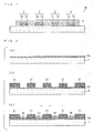
- Fig. 1 is a schematic sectional view of the printed circuit board according to the one embodiment of the present invention. As shown in Fig. 1 , a plurality of conductor traces 2 are formed on a porous base insulating layer 1 made of ePTFE (expanded polytetrafluoroethylene). Porous PTFE having continuous pores can be easily formed by using the ePTFE.
- ePTFE expanded polytetrafluoroethylene
- Each conductor trace 2 is a wiring trace or a ground trace.
- Each conductor trace 2 has a laminated structure of a seed layer 2a made of a laminated film of chromium and copper, for example, and a conductor layer 2b made of copper, for example.
- a cover insulating layer 3 is formed on the base insulating layer 1 to cover each conductor trace 2.
- the cover insulating layer 3 may be formed on the base insulating layer 1 to cover the entire conductor traces 2, or may be formed on the base insulating layer 1 to cover part of the conductor traces 2.
- the ePTFE used as the porous base insulating layer 1 has continuous pores.
- the average pore size of the ePTFE is not less than 0.05 ⁇ m and not more than 1.0 ⁇ m, preferably not less than 0.05 ⁇ m and not more than 0.2 ⁇ m, and more preferably not less than 0.05 ⁇ m and not more than 0.1 ⁇ m.
- the thickness of the porous base insulating layer 1 is not less than 1 ⁇ m and not more than 500 ⁇ m, preferably not less than 10 ⁇ m and not more than 200 ⁇ m, and more preferably not less than 10 ⁇ m and not more than 100 ⁇ m, for example.
- the porous base insulating layer 1 having the thickness of not more than 500 ⁇ m improves its flexibility, and the porous base insulating layer 1 having the thickness of not less than 1 ⁇ mimproves its insulation characteristics.
- the thickness of the seed layer 2a is preferably not less than 0.05 ⁇ m and not more than,1 ⁇ m.
- the thickness of each of the conductor traces 2 is not less than 1 ⁇ m and not more than 100 ⁇ m, and preferably not less than 10 ⁇ m and not more than 50 ⁇ m, for example.
- the thickness of the cover insulating layer 3 is not less than 1 ⁇ m and not more than 500 ⁇ m, preferably not less than 10 ⁇ m and not more than 200 ⁇ m, and more preferably not less than 10 ⁇ m and not more than 100 ⁇ m, for example.
- the cover insulating layer 3 having the thickness of not more than 500 ⁇ m improves its flexibility.
- the cover insulating layer 3 having the thickness of not less than 1 ⁇ m improves its insulation characteristics.
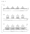
- Figs. 2 and 3 are sectional views for illustrating steps in a first method of manufacturing the printed circuit board 10.
- the example of Fig. 2 shows the method of manufacturing the printed circuit board 10 by a semi-additive method.
- the seed layer 2a made of the laminated film of chromium and copper is formed on the porous base insulating layer 1 made of ePTFE by a sputtering method, for example, as shown in Fig. 2 (a) .
- the seed layer 2a may be formed by electroless plating.
- the seed layer 2a is smoothed using a smoothing solution such as potassium persulfate (a smoothing step).
- a resist film is formed of a dry film resist or the like on the seed layer 2a, and the resist film is exposed using a mask having a given pattern, and then developed using a developing solution such as sodium carbonate (a developing step). In this manner, a plating resist 21 is formed on the seed layer 2a as shown in Fig. 2 (b) .
- the conductor layer 2b made of copper, for example, is subsequently formed on the seed layer 2a excluding a region of the plating resist 21 by electrolytic plating using a plating solution such as copper sulfate as shown in Fig. 2 (c) (a plating step).
- the plating resist 21 is removed by chemical etching (wet etching) or stripping using a stripping solution such as sodium hydrate as shown in Fig. 3 (a) (a stripping step).
- An exposed region of the seed layer 2a is then removed by etching using an etching solution such as ferric chloride (an etching step).
- the plurality of conductor traces 2 each composed of the seed layer 2a and the conductor layer 2b are formed as shown in Fig. 3 (b) .
- Each conductor trace 2 is a wiring trace or a ground trace, for example.
- the printed circuit board 10 is cleaned using pure water at a temperature of 20 °C or pure water at a temperature of 80 °C (a cleaning step) during or after the foregoing steps.
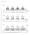
- Figs. 4 and 5 are sectional views for illustrating steps in a second method of manufacturing the printed circuit board 10.
- the example of Fig. 4 shows the method of manufacturing the printed circuit board 10 by a subtractive method.
- the seed layer 2a made of the laminated film of chromium and copper, for example, is formed on the porous base insulating layer 1 made of ePTFE by the sputtering method, for example, as shown in Fig. 4 (a) .
- the seed layer 2a may be formed by electroless plating.
- the conductor layer 2b made of copper is formed on the entire seed layer 2a by electrolytic plating using a plating solution such as copper sulfate as shown in Fig. 4 (b) (a plating step). After that, the conductor layer 2b is smoothed using a smoothing solution such as potassium persulfate (a smoothing step).
- a plating solution such as copper sulfate as shown in Fig. 4 (b)
- a smoothing solution such as potassium persulfate
- the resist film 22 is subsequently formed of a photosensitive dry film resist, for example, on the conductor layer 2b as shown in Fig. 4 (c) .
- the resist film 22 is exposed in the given pattern and then developed using the developing solution such as sodium carbonate or the like (a developing step), so that the etching resist 22a is formed as shown in Fig. 4 (d) .
- an exposed region of the conductor layer 2b and an exposed region of the seed layer 2a that are not covered with the etching resist 22a are removed by etching using the etching solution such as ferric chloride (an etching step) as shown in Fig. 5 (a) .
- the etching resist 22a is removed by the stripping solution such as sodium hydrate (a stripping step).
- the plurality of conductor traces 2 each composed of the seed layer 2a and the conductor layer 2b are formed as shown in Fig. 5 (b) .
- Each conductor trace 2 is a wiring trace or a ground trace, for example.
- the printed circuit board 10 is cleaned using pure water at a temperature of 20 °C or pure water at a temperature of 80 °C (a cleaning step) during or after the foregoing steps.
- the material for the cover insulating layer 3 is not limited to polyimide.
- ePTFE may be used similarly to the base insulating layer 1.
- the seed layer 2a may be a single layer film of chromium, for example, not limited to the laminated film of chromium and copper.
- the material for the conductor layer 2b is not limited to copper.
- another metal material such as a copper alloy, gold and aluminum may be used.
- the seed layer 2a may not be formed when the conductor layer 2b is formed by another method instead of the electrolytic plating.
- the ePTFE of the base insulating layer 1 has the continuous pores whose average pore size is not more than 1.0 ⁇ m. This prevents the processing solution from entering the continuous pores of the ePTFE when the conductor traces 2 are formed using the processing solution. Since the ePTFE has higher water repellency than other resin such as polyimide, the processing solution is prevented from remaining in the continuous pores even when the processing solution enters the continuous pores of the ePTFE.
- the relative dielectric constant of PTFE is 2.1, and the relative dielectric constant of polyimide is 3.5.
- the relative dielectric constant of the porous ePTFE having the continuous pores is even lower. This causes the dielectric constant of the base insulating layer 1 to be sufficiently lower than the dielectric constant of a base insulating layer made of other resin such as polyimide.
- the average pore size of the continuous pores of the ePTFE is not more than 0.2 ⁇ m, thereby sufficiently preventing the processing solution from entering the continuous pores of the ePTFE.
- the average pore size of the continuous pores of the ePTFE is not more than 0.1 ⁇ m, thereby more sufficiently preventing the processing solution from entering the continuous pores of the ePTFE.
- the dielectric constant of the base insulating layer 1 is reduced, resulting in lower loss to be caused by dielectrics of the conductor traces 2.
- the coefficient of friction of PTFE is smaller than the coefficient of friction of other resin such as polyimide, thus improving wear resistance of the base insulating layer 1.
- the printed circuit board 10 can be easily inserted into a narrow space, thus improving working efficiency.
- the modulus of elasticity of PTFE is smaller than the modulus of elasticity of other resin such as polyimide, flexibility and bending characteristics of the base insulating layer 1 can be improved.
- the resistivity of PTFE (not less than 1 ⁇ 10 18 ⁇ cm) is higher than the resistivity of polyimide (1 ⁇ 10 16 ⁇ ⁇ cm), thus eliminating the need to increase the thickness of the base insulating layer 1 in order to ensure insulation of the base insulating layer 1. This results in more improved flexibility and bending characteristics of the base insulating layer 1 than flexibility and bending characteristics of a base insulating layer made of other resin such as polyimide.
- the base insulating layer 1 is an example of an ,insulating layer
- the conductor trace 2 is an example of a conductor layer.
- inventive examples 1 to 5 and a comparative example 1 printed circuit boards 10 having porous base insulating layers 1 of different average pore sizes were manufactured based on the foregoing first method of manufacturing the printed circuit board.
- inventive examples 6 to 10 and a comparative example 2 printed circuit boards 10 having porous base insulating layers 1 of different average pore sizes were manufactured based on the foregoing second method of manufacturing the printed circuit board.
- PTFE porous films (TEMISH (registered trademark) NTF1121 by Nitto Denko Corporation) were used as the base insulating layers 1 in the printed circuit boards 10 of the inventive examples 1 and 6.
- the average pore size of the base insulating layer 1 was 0.1 ⁇ m, and the thickness of the base insulating layer 1 was 70 ⁇ m.
- PTFE porous films (TEMISH NTF1122 by Nitto Denko Corporation) were used as the base insulating layers 1 in the printed circuit boards 10 of the inventive examples 2 and 7.
- the average pore size of the base insulating layer 1 was 0.2 ⁇ m, and the thickness of the base insulating layer 1 was 75 ⁇ m.
- PTFE porous films (TEMISH NTF1125 by Nitto Denko Corporation) were used as the base insulating layers 1 in the printed circuit boards 10 of the inventive examples 3 and 8.
- the average pore size of the base insulating layer 1 was 0.5 ⁇ m, and the thickness of the base insulating layer 1 was 68 ⁇ m.
- PTFE porous films (TEMISH NTF1128 by Nitto Denko Corporation) were used as the base insulating layers 1 in the printed circuit boards 10 of the inventive examples 4 and 9.
- the average pore size of the base insulating layer 1 was 0.8 ⁇ m, and the thickness of the base insulating layer 1 was 80 ⁇ m.
- PTFE porous films (TEMISH NTF1131 by Nitto Denko Corporation) were used as the base insulating layers 1 in the printed circuit boards 10 of the inventive examples 5 and 10.
- the average pore size of the base insulating layer 1 was 1.0 ⁇ m, and the thickness of the base insulating layer 1 was 82 ⁇ m.
- PTFE porous films (TEMISH NTF1133 by Nitto Denko Corporation) were used as the base insulating layers 1 in the printed circuit boards 10 of the comparative examples 1 and 2.
- the average pore size of the base insulating layer 1 was 3.0 ⁇ m, and the thickness of the base insulating layer 1 was 86 ⁇ m.
- the seed layer 2a was made of the laminated film of chromium having a thickness of 50 nm and copper having a thickness of 100 nm.
- the thickness of the conductor layer 2b was 12 ⁇ m.
- the following processing solutions were used in the respective steps: an aqueous solution of copper sulfate in the plating step; an aqueous solution of potassium persulfate in the smoothing step; an aqueous solution of sodium carbonate in the developing step; an aqueous solution of ferric chloride in the etching step; an aqueous solution of sodium hydrate in the stripping step; and pure water at a temperature of 20 °C and pure water at a temperature of 80 °C in the cleaning step.
- Table 1 shows results of testing whether the processing solutions flow to the base insulating layer 1 in the printed circuit boards 10 of the inventive examples 1 to 5 and the comparative example 1.
- PROCESSING SOLUTION AQUEOUS SOLUTION
- INVENTIVE EXAMPLE 1 INVENTIVE EXAMPLE 2
- INVENTIVE EXAMPLE 3 INVENTIVE EXAMPLE 4
- COMPARATIVE EXAMPLE 1 0.1 ⁇ m 0.2 ⁇ m 0.5 ⁇ m 0.8 ⁇ m 1.0 ⁇ m 3.0 ⁇ m COPPER SULFATE ⁇ ⁇ ⁇ ⁇ ⁇ POTASSIUM PERSULFATE ⁇ ⁇ ⁇ ⁇ ⁇ SODIUM CARBONATE ⁇ ⁇ ⁇ ⁇ ⁇ ⁇ FERRIC CHLORIDE ⁇ ⁇ ⁇ ⁇ ⁇ SODIUM HYDRATE ⁇ ⁇ ⁇ ⁇ ⁇ PURE WATER (20 °C) ⁇ ⁇ ⁇ ⁇ ⁇ ⁇ ⁇ ⁇ ⁇
- the processing solutions did not flow to the back surface through the continuous pores of the base insulating layer 1 in the printed circuit boards 10 of the inventive examples 1 to 5. Moreover, the processing solutions did not remain in the continuous pores. Meanwhile, the processing solutions flowed to the back surface through the continuous pores of the base insulating layer 1 in the printed circuit board 10 of the comparative example 1. In addition, the processing solutions remained in the continuous pores.
- Table 2 shows results of testing whether the processing solutions flowed to the base insulating layer 1 in the printed circuit boards 10 of the inventive examples 6 to 10 and the comparative example 2.
- PROCESSING SOLUTION AQUEOUS SOLUTION
- INVENTIVE EXAMPLE 6 INVENTIVE EXAMPLE 7
- INVENTIVE EXAMPLE 8 INVENTIVE EXAMPLE 9
- INVENTIVE EXAMPLE 10 COMPARATIVE EXAMPLE 2 0.1 ⁇ m 0.2 ⁇ m 0.5 ⁇ m 0.8 ⁇ m 1.0 ⁇ m 3.0 ⁇ m COPPER SULFATE ⁇ ⁇ ⁇ ⁇ ⁇ POTASSIUM PERSULFATE ⁇ ⁇ ⁇ ⁇ ⁇ SODIUM CARBONATE ⁇ ⁇ ⁇ ⁇ ⁇ ⁇ FERRIC CHLORIDE ⁇ ⁇ ⁇ ⁇ ⁇ SODIUM HYDRATE ⁇ ⁇ ⁇ ⁇ ⁇ PURE WATER (20 °C) ⁇ ⁇ ⁇ ⁇ ⁇ ⁇
- the processing solutions did not flow to the back surface through the continuous pores of the base insulating layer 1 in the printed circuit boards 10 of the inventive examples 6 to 10. Moreover, the processing solutions did not remain in the continuous pores. Meanwhile, the processing solutions flowed to the back surface through the continuous pores of the base insulating layer 1 in the printed circuit board 10 of the comparative example 2. In addition, the processing solutions remained in the continuous pores.
- the results of the inventive examples 1 to 10 and the comparative examples 1, 2 show that when the average pore size of the porous base insulating layer 1 is not more than 1.0 ⁇ m, the processing solutions can be prevented from flowing to the back surface through the continuous pores of the base insulating layer 1 and from remaining in the continuous pores, regardless of the method of manufacturing the printed circuit board 10.
Landscapes
- Engineering & Computer Science (AREA)
- Microelectronics & Electronic Packaging (AREA)
- Physics & Mathematics (AREA)
- Spectroscopy & Molecular Physics (AREA)
- Manufacturing Of Printed Wiring (AREA)
- Laminated Bodies (AREA)
- Printing Elements For Providing Electric Connections Between Printed Circuits (AREA)
- Internal Circuitry In Semiconductor Integrated Circuit Devices (AREA)
- Non-Metallic Protective Coatings For Printed Circuits (AREA)
Claims (14)
- Verfahren zur Herstellung einer gedruckten Leiterplatte, umfassend die folgenden Schritte:Herstellen einer Isolierschicht (1), die aus einem porösen Material mit durchgehenden Poren gebildet ist; undAusbilden eines Leitermusters (2), das ein vorgegebenes Muster auf der Isolierschicht aufweist, unter Anwendung einer Verarbeitungslösung derart, dass die die Verarbeitungslösung daran gehindert wird, in die durchgehenden Poren der Isolierschicht einzudringen oder in denselben zu verweilen, wobeidas poröse Material poröses Polytetrafluorethylen umfasst, undeine durchschnittliche Porengröße der durchgehenden Poren des Polytetrafluorethylens nicht mehr als 1,0 µm ist.
- Verfahren nach Anspruch 1, wobei:die Verarbeitungslösung eine Entwicklungslösung umfasst, undder Schritt des Ausbildens des Leitermusters Folgendes umfasst:Ausbilden eines Resistfilms,Belichten des Resistfilms in einem vorgegebenen Muster,Ausbilden eines Plattierungs-Resists (21) durch Entwickeln des Resistfilms unter Anwendung der Verarbeitungslösung derart, dass die Entwicklungslösung daran gehindert wird, in die durchgehenden Poren der Isolierschicht einzudringen oder in denselben zu verweilen.
- Verfahren nach Anspruch 2, wobei:die Verarbeitungslösung eine Plattierungslösung umfasst, undder Schritt des Ausbildens des Leitermusters ferner Folgendes umfasst:
Ausbilden des Leitermusters unter Anwendung der Plattierungslösung, mit Ausnahme eines Bereichs des Plattierungs-Resists, derart, dass die Plattierungslösung daran gehindert wird, in die durchgehenden Poren der Isolierschicht einzudringen oder in denselben zu verweilen. - Verfahren nach Anspruch 3, wobei:die Verarbeitungslösung eine Stripplösung umfasst, undder Schritt des Ausbildens des Leitermusters ferner Folgendes umfasst:
Entfernen des Plattierungs-Resists unter Anwendung der Stripplösung derart, dass die Stripplösung daran gehindert wird, in die durchgehenden Poren der Isolierschicht einzudringen oder in denselben zu verweilen. - Verfahren gemäß einem der Ansprüche 2 bis 4, wobei:die Verarbeitungslösung eine Glättungslösung umfasst, unddas Ausbilden des Resistfilms Folgendes umfasst:Ausbilden einer Keimschicht (2a) auf der Isolierschicht,Glätten der Keimschicht unter Anwendung der Glättungslösung derart, dass die Glättungslösung daran gehindert wird, in die durchgehenden Poren der Isolierschicht einzudringen oder in denselben zu verweilen, undAusbilden des Resistfilms auf der Keimschicht.
- Verfahren gemäß Anspruch 5, wobei:die Verarbeitungslösung eine Ätzlösung umfasst, undein Strippen des Plattierungs-Resists ein Entfernen der Keimschicht durch Ätzen unter Anwendung der Ätzlösung derart umfasst, dass die Ätzlösung daran gehindert wird, in die durchgehenden Poren einzudringen oder in denselben zu verweilen.
- Verfahren nach Anspruch 1, wobei:die Verarbeitungslösung eine Plattierungslösung umfasst, undder Schritt des Ausbildens des Leitermusters Folgendes umfasst:
Ausbilden einer Leiterschicht (2b) unter Anwendung der Plattierungslösung derart, dass die Plattierungslösung daran gehindert wird, in die durchgehenden Poren der Isolierschicht einzudringen oder in denselben zu verweilen. - Verfahren nach Anspruch 7, wobei:die Verarbeitungslösung eine Entwicklungslösung umfasst, undder Schritt des Ausbildens des Leitermusters ferner Folgendes umfasst:Ausbilden eines Resistfilms (22) auf der Leiterschicht,Belichten des Resistfilms in einem vorgegebenen Muster, undAusbilden eines Ätzresists (22a) durch Entwickeln des Resistfilms unter Anwendung der Entwicklungslösung derart, dass die Entwicklungslösung daran gehindert wird, in die durchgehenden Poren der Isolierschicht einzudringen oder in denselben zu verweilen.
- Verfahren gemäß Anspruch 8, wobei:die Verarbeitungslösung eine Ätzlösung umfasst, undder Schritt des Ausbildens des Leitermusters ferner Folgendes umfasst:
Entfernen eines Bereichs der Leiterschicht durch Ätzen unter Anwendung der Ätzlösung, mit Ausnahme des Ätzresists, derart, dass die Ätzlösung daran gehindert wird, in die durchgehenden Poren der Isolierschicht einzudringen oder in denselben zu verweilen. - Verfahren gemäß Anspruch 9, wobei:die Verarbeitungslösung eine Stripplösung umfasst, undder Schritt des Ausbildens des Leitermusters ferner Folgendes umfasst:
Entfernen des Ätzresists durch Strippen unter Anwendung der Stripplösung derart, dass die Stripplösung daran gehindert wird, in die durchgehenden Poren der Isolierschicht einzudringen oder in denselben zu verweilen. - Verfahren gemäß einem der Ansprüche 7 bis 10, wobei:die Verarbeitungslösung eine Glättungslösung umfasst, unddas Ausbilden der Leiterschicht Folgendes umfasst:
Glätten der Leiterschicht unter Anwendung der Glättungslösung derart, dass die Glättungslösung daran gehindert wird, in die durchgehenden Poren der Isolierschicht einzudringen oder in denselben zu verweilen. - Verfahren gemäß einem der Ansprüche 1 bis 11, wobei die durchschnittliche Porengröße der durchgehenden Poren des Polytetrafluorethylens nicht mehr als 0,2 µm ist.
- Verfahren gemäß einem der Ansprüche 1 bis 12, wobei die durchschnittliche Porengröße der durchgehenden Poren des Polytetrafluorethylens nicht mehr als 0,1 µm ist.
- Verfahren gemäß einem der Ansprüche 1 bis 13, wobei das Polytetrafluorethylen geschäumtes Polytetrafluorethylen ist.
Applications Claiming Priority (1)
| Application Number | Priority Date | Filing Date | Title |
|---|---|---|---|
| JP2010172617A JP5528250B2 (ja) | 2010-07-30 | 2010-07-30 | 配線回路基板の製造方法 |
Publications (3)
| Publication Number | Publication Date |
|---|---|
| EP2413674A2 EP2413674A2 (de) | 2012-02-01 |
| EP2413674A3 EP2413674A3 (de) | 2012-10-03 |
| EP2413674B1 true EP2413674B1 (de) | 2018-08-01 |
Family
ID=44882635
Family Applications (1)
| Application Number | Title | Priority Date | Filing Date |
|---|---|---|---|
| EP11164848.1A Not-in-force EP2413674B1 (de) | 2010-07-30 | 2011-05-04 | Herstellungsverfahren für Leiterplatte |
Country Status (6)
| Country | Link |
|---|---|
| US (1) | US9288903B2 (de) |
| EP (1) | EP2413674B1 (de) |
| JP (1) | JP5528250B2 (de) |
| KR (1) | KR101902015B1 (de) |
| CN (1) | CN102378483B (de) |
| TW (1) | TWI541835B (de) |
Families Citing this family (10)
| Publication number | Priority date | Publication date | Assignee | Title |
|---|---|---|---|---|
| CN102260378B (zh) * | 2011-05-06 | 2013-03-20 | 广东生益科技股份有限公司 | 复合材料、用其制作的高频电路基板及其制作方法 |
| US9666514B2 (en) * | 2015-04-14 | 2017-05-30 | Invensas Corporation | High performance compliant substrate |
| US11535017B2 (en) | 2017-04-04 | 2022-12-27 | W. L. Gore & Associates Gmbh | Dielectric composite with reinforced elastomer and integrate electrode |
| CN107446156A (zh) * | 2017-08-22 | 2017-12-08 | 江苏泛亚微透科技股份有限公司 | 在膨体聚四氟乙烯膜面上涂布石墨烯涂层的复合材料、其制备方法及其制备装置 |
| KR20190031838A (ko) * | 2017-09-18 | 2019-03-27 | 주식회사 아모그린텍 | 박막 회로 기판 및 이의 제조 방법 |
| AU2018422666B2 (en) | 2018-05-08 | 2022-03-10 | W. L. Gore & Associates, Inc. | Flexible and stretchable printed circuits on stretchable substrates |
| JP7089064B2 (ja) | 2018-05-08 | 2022-06-21 | ダブリュ.エル.ゴア アンド アソシエイツ,インコーポレイティド | 皮膚適用のためのフレキシブルプリント回路 |
| US11330711B2 (en) | 2018-05-08 | 2022-05-10 | W. L. Gore & Associates, Inc. | Flexible and durable printed circuits on stretchable and non-stretchable substrates |
| JP7166122B2 (ja) * | 2018-09-28 | 2022-11-07 | 日東電工株式会社 | ロール体 |
| US12114437B2 (en) * | 2020-06-24 | 2024-10-08 | Resonac Corporation | Wiring structure, method for manufacturing same, and semiconductor package |
Family Cites Families (27)
| Publication number | Priority date | Publication date | Assignee | Title |
|---|---|---|---|---|
| JPS5476668A (en) * | 1977-11-30 | 1979-06-19 | Nitto Electric Ind Co Ltd | Production of porous polytetrafluoroethylene film |
| JPS60214941A (ja) | 1984-04-10 | 1985-10-28 | 株式会社 潤工社 | プリント基板 |
| JPS60225750A (ja) * | 1984-04-24 | 1985-11-11 | 株式会社 潤工社 | プリント基板 |
| JPS6442890A (en) * | 1987-08-11 | 1989-02-15 | Japan Gore Tex Inc | Printed substrate |
| JP2559236B2 (ja) * | 1987-09-10 | 1996-12-04 | ジャパンゴアテックス株式会社 | シート材 |
| JPH02296389A (ja) * | 1989-05-11 | 1990-12-06 | Japan Gore Tex Inc | 印刷回路基板 |
| JPH05243697A (ja) * | 1992-03-03 | 1993-09-21 | Japan Gore Tex Inc | 誘電体基板 |
| JPH06224526A (ja) * | 1993-01-27 | 1994-08-12 | Japan Gore Tex Inc | 誘電体基板 |
| JPH06244537A (ja) * | 1993-02-19 | 1994-09-02 | Junkosha Co Ltd | プリント配線板 |
| JPH09302121A (ja) | 1996-05-17 | 1997-11-25 | Nitto Denko Corp | ポリテトラフルオロエチレン多孔質膜の製造方法 |
| US5910354A (en) * | 1997-03-04 | 1999-06-08 | W.L. Gore & Associates, Inc. | Metallurgical interconnect composite |
| JP4110669B2 (ja) | 1999-05-13 | 2008-07-02 | 宇部興産株式会社 | 多孔質絶縁材料およびその積層体 |
| US20030129379A1 (en) | 1999-04-23 | 2003-07-10 | Shigeru Yao | Porous insulating film and its laminates |
| US6899999B2 (en) * | 2001-03-28 | 2005-05-31 | Kabushiki Kaisha Toshiba | Method of manufacturing composite member, photosensitive composition, porous base material, insulating body and composite member |
| TW545092B (en) | 2001-10-25 | 2003-08-01 | Matsushita Electric Industrial Co Ltd | Prepreg and circuit board and method for manufacturing the same |
| JP2003200535A (ja) | 2001-10-25 | 2003-07-15 | Matsushita Electric Ind Co Ltd | プリプレグおよび回路基板、ならびにそれらの製造方法 |
| ATE428291T1 (de) * | 2001-12-21 | 2009-04-15 | Ifire Ip Corp | Dielektrische dickschicht mit niedriger brenntemperatur fur elektrolumineszierende vorrichtungen |
| JP2003201362A (ja) | 2002-01-09 | 2003-07-18 | Hitachi Ltd | 多孔質ポリイミドフィルムおよび多孔質ポリイミド回路基板 |
| JP2004082372A (ja) * | 2002-08-23 | 2004-03-18 | Nitto Denko Corp | 高周波配線基板用絶縁材及び高周波用配線基板 |
| JP4380466B2 (ja) | 2004-08-23 | 2009-12-09 | 住友電気工業株式会社 | 穿孔された多孔質樹脂基材及び穿孔の内壁面を導電化した多孔質樹脂基材の製造方法 |
| KR101058309B1 (ko) * | 2006-01-13 | 2011-08-22 | 파나소닉 주식회사 | 입체 회로 기판 및 그 제조 방법 |
| KR100836653B1 (ko) | 2006-10-25 | 2008-06-10 | 삼성전기주식회사 | 회로기판 및 그 제조방법 |
| JP5051355B2 (ja) | 2007-04-06 | 2012-10-17 | 日立電線株式会社 | プリント配線基板の製造方法 |
| JP2008300238A (ja) * | 2007-05-31 | 2008-12-11 | Nitto Denko Corp | 配線回路基板および燃料電池 |
| US7787256B2 (en) * | 2007-08-10 | 2010-08-31 | Gore Enterprise Holdings, Inc. | Tamper respondent system |
| JP5238274B2 (ja) | 2008-01-31 | 2013-07-17 | 日東電工株式会社 | 配線回路基板およびその製造方法 |
| US8755196B2 (en) * | 2010-07-09 | 2014-06-17 | Ibiden Co., Ltd. | Wiring board and method for manufacturing the same |
-
2010
- 2010-07-30 JP JP2010172617A patent/JP5528250B2/ja active Active
-
2011
- 2011-04-22 TW TW100114056A patent/TWI541835B/zh active
- 2011-04-27 US US13/094,941 patent/US9288903B2/en not_active Expired - Fee Related
- 2011-05-04 EP EP11164848.1A patent/EP2413674B1/de not_active Not-in-force
- 2011-06-28 KR KR1020110062650A patent/KR101902015B1/ko active Active
- 2011-07-29 CN CN201110217062.4A patent/CN102378483B/zh active Active
Non-Patent Citations (1)
| Title |
|---|
| None * |
Also Published As
| Publication number | Publication date |
|---|---|
| KR101902015B1 (ko) | 2018-09-27 |
| TW201212046A (en) | 2012-03-16 |
| EP2413674A2 (de) | 2012-02-01 |
| CN102378483B (zh) | 2015-12-02 |
| EP2413674A3 (de) | 2012-10-03 |
| JP2012033752A (ja) | 2012-02-16 |
| KR20120012384A (ko) | 2012-02-09 |
| JP5528250B2 (ja) | 2014-06-25 |
| TWI541835B (zh) | 2016-07-11 |
| CN102378483A (zh) | 2012-03-14 |
| US20120024581A1 (en) | 2012-02-02 |
| US9288903B2 (en) | 2016-03-15 |
Similar Documents
| Publication | Publication Date | Title |
|---|---|---|
| EP2413674A2 (de) | Leiterplatte und Herstellungsverfahren dafür | |
| US10993331B2 (en) | High-speed interconnects for printed circuit boards | |
| US9538642B2 (en) | Wiring board and method for manufacturing the same | |
| US8138423B2 (en) | Printed wiring board and method for manufacturing printed wiring board | |
| JP2007235164A (ja) | 多層プリント配線板 | |
| KR101421701B1 (ko) | 연성회로 동장 적층판과 이를 이용한 인쇄회로 기판 및 그 제조 방법 | |
| US20210392754A1 (en) | Printed wiring board and manufacturing method thereof | |
| JP2006148079A (ja) | 平滑な側面を有する3つの導電層を一部として使用する回路基板、その製造方法、ならびにこの回路基板を使用する電気組立体および情報処理システム | |
| KR101421702B1 (ko) | 연성회로 동장 적층판과 이를 이용한 인쇄회로 기판 및 그 제조 방법 | |
| JP4129166B2 (ja) | 電解銅箔、電解銅箔付きフィルム及び多層配線基板と、その製造方法 | |
| KR101149026B1 (ko) | 양면 연성 인쇄회로기판 및 그 제조 방법 | |
| EP1613135B1 (de) | Leiterplatte und Verfahren zur Herstellung einer Leiterplatte | |
| KR101421703B1 (ko) | 연성회로 동장 적층판과 이를 이용한 인쇄회로 기판 및 그 제조 방법 | |
| JPH05183259A (ja) | 高密度プリント配線板の製造方法 | |
| JP3728068B2 (ja) | 多層配線基板 | |
| KR101357141B1 (ko) | 연성회로 동장 적층판과 이를 이용한 인쇄회로 기판 및 그 제조 방법 | |
| US20220336342A1 (en) | Wiring Trace Morphology Structure for High Speed Applications | |
| JP2012216759A (ja) | プリント配線基板の製造方法、プリント配線基板 | |
| JPH11199738A (ja) | フッ素樹脂組成物および多層プリント配線板 | |
| JP2003115663A (ja) | 多層プリント配線板 | |
| JPH0541580A (ja) | 多層回路基板 | |
| US20120090172A1 (en) | Method of manufacturing printed circuit boad | |
| Takashi et al. | Development of novel polyimide build-up material | |
| JP2006135166A (ja) | プリント配線板 | |
| JP2002299825A (ja) | 多層回路基板 |
Legal Events
| Date | Code | Title | Description |
|---|---|---|---|
| AK | Designated contracting states |
Kind code of ref document: A2 Designated state(s): AL AT BE BG CH CY CZ DE DK EE ES FI FR GB GR HR HU IE IS IT LI LT LU LV MC MK MT NL NO PL PT RO RS SE SI SK SM TR |
|
| AX | Request for extension of the european patent |
Extension state: BA ME |
|
| PUAI | Public reference made under article 153(3) epc to a published international application that has entered the european phase |
Free format text: ORIGINAL CODE: 0009012 |
|
| PUAL | Search report despatched |
Free format text: ORIGINAL CODE: 0009013 |
|
| AK | Designated contracting states |
Kind code of ref document: A3 Designated state(s): AL AT BE BG CH CY CZ DE DK EE ES FI FR GB GR HR HU IE IS IT LI LT LU LV MC MK MT NL NO PL PT RO RS SE SI SK SM TR |
|
| AX | Request for extension of the european patent |
Extension state: BA ME |
|
| RIC1 | Information provided on ipc code assigned before grant |
Ipc: C08L 27/12 20060101ALI20120827BHEP Ipc: C08J 5/18 20060101ALI20120827BHEP Ipc: H05K 1/03 20060101AFI20120827BHEP Ipc: H01M 8/10 20060101ALI20120827BHEP Ipc: H01B 3/44 20060101ALI20120827BHEP |
|
| 17P | Request for examination filed |
Effective date: 20130312 |
|
| GRAP | Despatch of communication of intention to grant a patent |
Free format text: ORIGINAL CODE: EPIDOSNIGR1 |
|
| STAA | Information on the status of an ep patent application or granted ep patent |
Free format text: STATUS: GRANT OF PATENT IS INTENDED |
|
| RIC1 | Information provided on ipc code assigned before grant |
Ipc: H05K 3/06 20060101ALN20180130BHEP Ipc: H05K 3/10 20060101ALN20180130BHEP Ipc: H05K 1/03 20060101AFI20180130BHEP Ipc: H01M 8/10 20160101ALI20180130BHEP Ipc: C08L 27/12 20060101ALI20180130BHEP Ipc: C08J 5/18 20060101ALI20180130BHEP Ipc: H01B 3/44 20060101ALI20180130BHEP |
|
| INTG | Intention to grant announced |
Effective date: 20180227 |
|
| GRAS | Grant fee paid |
Free format text: ORIGINAL CODE: EPIDOSNIGR3 |
|
| GRAA | (expected) grant |
Free format text: ORIGINAL CODE: 0009210 |
|
| STAA | Information on the status of an ep patent application or granted ep patent |
Free format text: STATUS: THE PATENT HAS BEEN GRANTED |
|
| AK | Designated contracting states |
Kind code of ref document: B1 Designated state(s): AL AT BE BG CH CY CZ DE DK EE ES FI FR GB GR HR HU IE IS IT LI LT LU LV MC MK MT NL NO PL PT RO RS SE SI SK SM TR |
|
| REG | Reference to a national code |
Ref country code: GB Ref legal event code: FG4D |
|
| REG | Reference to a national code |
Ref country code: CH Ref legal event code: EP Ref country code: AT Ref legal event code: REF Ref document number: 1025904 Country of ref document: AT Kind code of ref document: T Effective date: 20180815 |
|
| REG | Reference to a national code |
Ref country code: IE Ref legal event code: FG4D |
|
| REG | Reference to a national code |
Ref country code: DE Ref legal event code: R096 Ref document number: 602011050502 Country of ref document: DE |
|
| REG | Reference to a national code |
Ref country code: NL Ref legal event code: MP Effective date: 20180801 |
|
| REG | Reference to a national code |
Ref country code: LT Ref legal event code: MG4D |
|
| REG | Reference to a national code |
Ref country code: AT Ref legal event code: MK05 Ref document number: 1025904 Country of ref document: AT Kind code of ref document: T Effective date: 20180801 |
|
| PG25 | Lapsed in a contracting state [announced via postgrant information from national office to epo] |
Ref country code: BG Free format text: LAPSE BECAUSE OF FAILURE TO SUBMIT A TRANSLATION OF THE DESCRIPTION OR TO PAY THE FEE WITHIN THE PRESCRIBED TIME-LIMIT Effective date: 20181101 Ref country code: GR Free format text: LAPSE BECAUSE OF FAILURE TO SUBMIT A TRANSLATION OF THE DESCRIPTION OR TO PAY THE FEE WITHIN THE PRESCRIBED TIME-LIMIT Effective date: 20181102 Ref country code: NO Free format text: LAPSE BECAUSE OF FAILURE TO SUBMIT A TRANSLATION OF THE DESCRIPTION OR TO PAY THE FEE WITHIN THE PRESCRIBED TIME-LIMIT Effective date: 20181101 Ref country code: IS Free format text: LAPSE BECAUSE OF FAILURE TO SUBMIT A TRANSLATION OF THE DESCRIPTION OR TO PAY THE FEE WITHIN THE PRESCRIBED TIME-LIMIT Effective date: 20181201 Ref country code: AT Free format text: LAPSE BECAUSE OF FAILURE TO SUBMIT A TRANSLATION OF THE DESCRIPTION OR TO PAY THE FEE WITHIN THE PRESCRIBED TIME-LIMIT Effective date: 20180801 Ref country code: FI Free format text: LAPSE BECAUSE OF FAILURE TO SUBMIT A TRANSLATION OF THE DESCRIPTION OR TO PAY THE FEE WITHIN THE PRESCRIBED TIME-LIMIT Effective date: 20180801 Ref country code: RS Free format text: LAPSE BECAUSE OF FAILURE TO SUBMIT A TRANSLATION OF THE DESCRIPTION OR TO PAY THE FEE WITHIN THE PRESCRIBED TIME-LIMIT Effective date: 20180801 Ref country code: NL Free format text: LAPSE BECAUSE OF FAILURE TO SUBMIT A TRANSLATION OF THE DESCRIPTION OR TO PAY THE FEE WITHIN THE PRESCRIBED TIME-LIMIT Effective date: 20180801 Ref country code: LT Free format text: LAPSE BECAUSE OF FAILURE TO SUBMIT A TRANSLATION OF THE DESCRIPTION OR TO PAY THE FEE WITHIN THE PRESCRIBED TIME-LIMIT Effective date: 20180801 Ref country code: SE Free format text: LAPSE BECAUSE OF FAILURE TO SUBMIT A TRANSLATION OF THE DESCRIPTION OR TO PAY THE FEE WITHIN THE PRESCRIBED TIME-LIMIT Effective date: 20180801 Ref country code: PL Free format text: LAPSE BECAUSE OF FAILURE TO SUBMIT A TRANSLATION OF THE DESCRIPTION OR TO PAY THE FEE WITHIN THE PRESCRIBED TIME-LIMIT Effective date: 20180801 |
|
| PG25 | Lapsed in a contracting state [announced via postgrant information from national office to epo] |
Ref country code: AL Free format text: LAPSE BECAUSE OF FAILURE TO SUBMIT A TRANSLATION OF THE DESCRIPTION OR TO PAY THE FEE WITHIN THE PRESCRIBED TIME-LIMIT Effective date: 20180801 Ref country code: LV Free format text: LAPSE BECAUSE OF FAILURE TO SUBMIT A TRANSLATION OF THE DESCRIPTION OR TO PAY THE FEE WITHIN THE PRESCRIBED TIME-LIMIT Effective date: 20180801 Ref country code: HR Free format text: LAPSE BECAUSE OF FAILURE TO SUBMIT A TRANSLATION OF THE DESCRIPTION OR TO PAY THE FEE WITHIN THE PRESCRIBED TIME-LIMIT Effective date: 20180801 Ref country code: ES Free format text: LAPSE BECAUSE OF FAILURE TO SUBMIT A TRANSLATION OF THE DESCRIPTION OR TO PAY THE FEE WITHIN THE PRESCRIBED TIME-LIMIT Effective date: 20180801 |
|
| PG25 | Lapsed in a contracting state [announced via postgrant information from national office to epo] |
Ref country code: CZ Free format text: LAPSE BECAUSE OF FAILURE TO SUBMIT A TRANSLATION OF THE DESCRIPTION OR TO PAY THE FEE WITHIN THE PRESCRIBED TIME-LIMIT Effective date: 20180801 Ref country code: IT Free format text: LAPSE BECAUSE OF FAILURE TO SUBMIT A TRANSLATION OF THE DESCRIPTION OR TO PAY THE FEE WITHIN THE PRESCRIBED TIME-LIMIT Effective date: 20180801 Ref country code: RO Free format text: LAPSE BECAUSE OF FAILURE TO SUBMIT A TRANSLATION OF THE DESCRIPTION OR TO PAY THE FEE WITHIN THE PRESCRIBED TIME-LIMIT Effective date: 20180801 Ref country code: EE Free format text: LAPSE BECAUSE OF FAILURE TO SUBMIT A TRANSLATION OF THE DESCRIPTION OR TO PAY THE FEE WITHIN THE PRESCRIBED TIME-LIMIT Effective date: 20180801 |
|
| REG | Reference to a national code |
Ref country code: DE Ref legal event code: R097 Ref document number: 602011050502 Country of ref document: DE |
|
| PG25 | Lapsed in a contracting state [announced via postgrant information from national office to epo] |
Ref country code: SK Free format text: LAPSE BECAUSE OF FAILURE TO SUBMIT A TRANSLATION OF THE DESCRIPTION OR TO PAY THE FEE WITHIN THE PRESCRIBED TIME-LIMIT Effective date: 20180801 Ref country code: DK Free format text: LAPSE BECAUSE OF FAILURE TO SUBMIT A TRANSLATION OF THE DESCRIPTION OR TO PAY THE FEE WITHIN THE PRESCRIBED TIME-LIMIT Effective date: 20180801 Ref country code: SM Free format text: LAPSE BECAUSE OF FAILURE TO SUBMIT A TRANSLATION OF THE DESCRIPTION OR TO PAY THE FEE WITHIN THE PRESCRIBED TIME-LIMIT Effective date: 20180801 |
|
| PLBE | No opposition filed within time limit |
Free format text: ORIGINAL CODE: 0009261 |
|
| STAA | Information on the status of an ep patent application or granted ep patent |
Free format text: STATUS: NO OPPOSITION FILED WITHIN TIME LIMIT |
|
| 26N | No opposition filed |
Effective date: 20190503 |
|
| PG25 | Lapsed in a contracting state [announced via postgrant information from national office to epo] |
Ref country code: SI Free format text: LAPSE BECAUSE OF FAILURE TO SUBMIT A TRANSLATION OF THE DESCRIPTION OR TO PAY THE FEE WITHIN THE PRESCRIBED TIME-LIMIT Effective date: 20180801 |
|
| REG | Reference to a national code |
Ref country code: CH Ref legal event code: PL |
|
| PG25 | Lapsed in a contracting state [announced via postgrant information from national office to epo] |
Ref country code: MC Free format text: LAPSE BECAUSE OF FAILURE TO SUBMIT A TRANSLATION OF THE DESCRIPTION OR TO PAY THE FEE WITHIN THE PRESCRIBED TIME-LIMIT Effective date: 20180801 Ref country code: LI Free format text: LAPSE BECAUSE OF NON-PAYMENT OF DUE FEES Effective date: 20190531 Ref country code: CH Free format text: LAPSE BECAUSE OF NON-PAYMENT OF DUE FEES Effective date: 20190531 |
|
| REG | Reference to a national code |
Ref country code: BE Ref legal event code: MM Effective date: 20190531 |
|
| PG25 | Lapsed in a contracting state [announced via postgrant information from national office to epo] |
Ref country code: LU Free format text: LAPSE BECAUSE OF NON-PAYMENT OF DUE FEES Effective date: 20190504 |
|
| PG25 | Lapsed in a contracting state [announced via postgrant information from national office to epo] |
Ref country code: TR Free format text: LAPSE BECAUSE OF FAILURE TO SUBMIT A TRANSLATION OF THE DESCRIPTION OR TO PAY THE FEE WITHIN THE PRESCRIBED TIME-LIMIT Effective date: 20180801 |
|
| PG25 | Lapsed in a contracting state [announced via postgrant information from national office to epo] |
Ref country code: IE Free format text: LAPSE BECAUSE OF NON-PAYMENT OF DUE FEES Effective date: 20190504 |
|
| PG25 | Lapsed in a contracting state [announced via postgrant information from national office to epo] |
Ref country code: BE Free format text: LAPSE BECAUSE OF NON-PAYMENT OF DUE FEES Effective date: 20190531 |
|
| PG25 | Lapsed in a contracting state [announced via postgrant information from national office to epo] |
Ref country code: PT Free format text: LAPSE BECAUSE OF FAILURE TO SUBMIT A TRANSLATION OF THE DESCRIPTION OR TO PAY THE FEE WITHIN THE PRESCRIBED TIME-LIMIT Effective date: 20181201 |
|
| PG25 | Lapsed in a contracting state [announced via postgrant information from national office to epo] |
Ref country code: CY Free format text: LAPSE BECAUSE OF FAILURE TO SUBMIT A TRANSLATION OF THE DESCRIPTION OR TO PAY THE FEE WITHIN THE PRESCRIBED TIME-LIMIT Effective date: 20180801 |
|
| PG25 | Lapsed in a contracting state [announced via postgrant information from national office to epo] |
Ref country code: HU Free format text: LAPSE BECAUSE OF FAILURE TO SUBMIT A TRANSLATION OF THE DESCRIPTION OR TO PAY THE FEE WITHIN THE PRESCRIBED TIME-LIMIT; INVALID AB INITIO Effective date: 20110504 Ref country code: MT Free format text: LAPSE BECAUSE OF FAILURE TO SUBMIT A TRANSLATION OF THE DESCRIPTION OR TO PAY THE FEE WITHIN THE PRESCRIBED TIME-LIMIT Effective date: 20180801 |
|
| PGFP | Annual fee paid to national office [announced via postgrant information from national office to epo] |
Ref country code: DE Payment date: 20210408 Year of fee payment: 11 Ref country code: FR Payment date: 20210412 Year of fee payment: 11 |
|
| PGFP | Annual fee paid to national office [announced via postgrant information from national office to epo] |
Ref country code: GB Payment date: 20210408 Year of fee payment: 11 |
|
| PG25 | Lapsed in a contracting state [announced via postgrant information from national office to epo] |
Ref country code: MK Free format text: LAPSE BECAUSE OF FAILURE TO SUBMIT A TRANSLATION OF THE DESCRIPTION OR TO PAY THE FEE WITHIN THE PRESCRIBED TIME-LIMIT Effective date: 20180801 |
|
| REG | Reference to a national code |
Ref country code: DE Ref legal event code: R119 Ref document number: 602011050502 Country of ref document: DE |
|
| GBPC | Gb: european patent ceased through non-payment of renewal fee |
Effective date: 20220504 |
|
| PG25 | Lapsed in a contracting state [announced via postgrant information from national office to epo] |
Ref country code: FR Free format text: LAPSE BECAUSE OF NON-PAYMENT OF DUE FEES Effective date: 20220531 |
|
| PG25 | Lapsed in a contracting state [announced via postgrant information from national office to epo] |
Ref country code: GB Free format text: LAPSE BECAUSE OF NON-PAYMENT OF DUE FEES Effective date: 20220504 Ref country code: DE Free format text: LAPSE BECAUSE OF NON-PAYMENT OF DUE FEES Effective date: 20221201 |