EP2408267B1 - Serial controller and bi-directional serial controller for LED lights - Google Patents
Serial controller and bi-directional serial controller for LED lights Download PDFInfo
- Publication number
- EP2408267B1 EP2408267B1 EP10189052.3A EP10189052A EP2408267B1 EP 2408267 B1 EP2408267 B1 EP 2408267B1 EP 10189052 A EP10189052 A EP 10189052A EP 2408267 B1 EP2408267 B1 EP 2408267B1
- Authority
- EP
- European Patent Office
- Prior art keywords
- signal
- serial
- output
- clock
- cki
- Prior art date
- Legal status (The legal status is an assumption and is not a legal conclusion. Google has not performed a legal analysis and makes no representation as to the accuracy of the status listed.)
- Active
Links
Images


Classifications
-
- H—ELECTRICITY
- H05—ELECTRIC TECHNIQUES NOT OTHERWISE PROVIDED FOR
- H05B—ELECTRIC HEATING; ELECTRIC LIGHT SOURCES NOT OTHERWISE PROVIDED FOR; CIRCUIT ARRANGEMENTS FOR ELECTRIC LIGHT SOURCES, IN GENERAL
- H05B45/00—Circuit arrangements for operating light-emitting diodes [LED]
-
- H—ELECTRICITY
- H05—ELECTRIC TECHNIQUES NOT OTHERWISE PROVIDED FOR
- H05B—ELECTRIC HEATING; ELECTRIC LIGHT SOURCES NOT OTHERWISE PROVIDED FOR; CIRCUIT ARRANGEMENTS FOR ELECTRIC LIGHT SOURCES, IN GENERAL
- H05B45/00—Circuit arrangements for operating light-emitting diodes [LED]
- H05B45/30—Driver circuits
-
- H—ELECTRICITY
- H05—ELECTRIC TECHNIQUES NOT OTHERWISE PROVIDED FOR
- H05B—ELECTRIC HEATING; ELECTRIC LIGHT SOURCES NOT OTHERWISE PROVIDED FOR; CIRCUIT ARRANGEMENTS FOR ELECTRIC LIGHT SOURCES, IN GENERAL
- H05B45/00—Circuit arrangements for operating light-emitting diodes [LED]
- H05B45/40—Details of LED load circuits
- H05B45/44—Details of LED load circuits with an active control inside an LED matrix
- H05B45/46—Details of LED load circuits with an active control inside an LED matrix having LEDs disposed in parallel lines
-
- H—ELECTRICITY
- H05—ELECTRIC TECHNIQUES NOT OTHERWISE PROVIDED FOR
- H05B—ELECTRIC HEATING; ELECTRIC LIGHT SOURCES NOT OTHERWISE PROVIDED FOR; CIRCUIT ARRANGEMENTS FOR ELECTRIC LIGHT SOURCES, IN GENERAL
- H05B47/00—Circuit arrangements for operating light sources in general, i.e. where the type of light source is not relevant
- H05B47/10—Controlling the light source
- H05B47/175—Controlling the light source by remote control
- H05B47/18—Controlling the light source by remote control via data-bus transmission
-
- H—ELECTRICITY
- H05—ELECTRIC TECHNIQUES NOT OTHERWISE PROVIDED FOR
- H05B—ELECTRIC HEATING; ELECTRIC LIGHT SOURCES NOT OTHERWISE PROVIDED FOR; CIRCUIT ARRANGEMENTS FOR ELECTRIC LIGHT SOURCES, IN GENERAL
- H05B45/00—Circuit arrangements for operating light-emitting diodes [LED]
- H05B45/30—Driver circuits
- H05B45/32—Pulse-control circuits
- H05B45/325—Pulse-width modulation [PWM]
-
- H—ELECTRICITY
- H05—ELECTRIC TECHNIQUES NOT OTHERWISE PROVIDED FOR
- H05B—ELECTRIC HEATING; ELECTRIC LIGHT SOURCES NOT OTHERWISE PROVIDED FOR; CIRCUIT ARRANGEMENTS FOR ELECTRIC LIGHT SOURCES, IN GENERAL
- H05B47/00—Circuit arrangements for operating light sources in general, i.e. where the type of light source is not relevant
- H05B47/10—Controlling the light source
- H05B47/175—Controlling the light source by remote control
- H05B47/18—Controlling the light source by remote control via data-bus transmission
- H05B47/184—Controlling the light source by remote control via data-bus transmission using digital multiplexed [DMX] communication protocols
Definitions
- the present invention relates to a serial controller and a bi-directional serial controller, and more particularly to a serial controller and a bi-directional serial controller for synchronously transmitting data signals at all stages in a series with an inverted clock.
- LEDs light-emitting diodes
- the RGB cluster formed by red, blue and green LEDs has diversified light and shadow changing effects
- the RGB cluster is usually connected in series for different illuminators so as to form a strip screen, curtain display, or wall washer light of multilevel serial spot lights, which is applied in the long-distance light string.
- this kind of illumination apparatus is usually designed according to the appearance of the building or different commercial requirements, when the range of appearance of the building demanding for illumination is large or the design of the illuminator is complicated, the designer needs to connect in series a large number of spot lights, LEDs, and the driving clocks thereof so as to form a long string of RGB cluster, thereby achieving a better illumination effect.
- the problem of this serial RGB cluster lies in that the driving clock for driving the spot lights at each stage in the series is not a single global signal. That is to say, the driving clock of the spot lights at each stage is obtained from the driving clock of the spot lights in the previous stage. Therefore, regarding the signal of the driving clock at one stage in the series, when the duty cycle of the driving clock offsets due to the capacitance effect or accumulative effect generated in the transmission distance, e.g., the time of the signal of the driving clock at the high level is unequal to the time of the signal at the low level, and in this circumstance, for the serial RGB cluster formed by connecting multilevel spot lights in series, the signal waveform of the driving clock of the spot lights at the latter level is severely distorted due to the multilevel accumulative effect.
- the present invention is a serial controller, which not only drives and serially connects the spot lights at all stages but also solves the waveform distortion problem of the driving clocks of the spot lights at all stages in the series.
- the present invention is further a bi-directional serial controller for realizing bi-directional transmission of the data signals between the spot lights at all stages.
- the present invention provides a serial controller, adapted to receive an external clock and an input data and output an inverted clock and an output data.
- the serial controller comprises an inverter, a serial position detector, a synchronous clock generator, a serial register, and a half-cycle delay unit.
- the inverter receives the external clock and outputs the inverted clock.
- the serial position detector outputs a position signal according to the external clock and the input data, wherein the position signal is an odd signal or an even signal.
- the synchronous clock generator outputs a synchronous clock according to the position signal and the external clock.
- the position signal is the odd signal
- the synchronous clock and the external clock are in the same phase
- the position signal is the even signal
- the synchronous clock and the external clock are in the opposite phase.
- the serial register receives and temporarily stores the input data according to the synchronous clock and then outputs the data.
- the half-cycle delay unit receives the data from the serial register, delays the data by a half cycle of the synchronous clock, and outputs the data as the output data.
- the present invention further provides a bi-directional serial controller, which comprises an inverter, an input contact, a serial position detector, a synchronous clock generator, a serial register, an identification unit, a half-cycle delay unit, an output contact, and a data directing unit.
- a bi-directional serial controller which comprises an inverter, an input contact, a serial position detector, a synchronous clock generator, a serial register, an identification unit, a half-cycle delay unit, an output contact, and a data directing unit.
- the inverter receives and inverts an external clock and then outputs an inverted clock.
- the input contact receives an input data.
- the serial position detector outputs a position signal according to the external clock and the input data, wherein the position signal is an odd signal or an even signal.
- the synchronous clock generator outputs a synchronous clock according to the position signal and the external clock.
- the position signal is the odd signal
- the synchronous clock and the external clock are in the same phase
- the position signal is the even signal
- the synchronous clock and the external clock are in the opposite phase.
- the serial register has a receiving end and a transmitting end.
- the serial register stores the signal received by the receiving end according to the synchronous clock and then outputs the signal from the transmitting end.
- the identification unit outputs a control signal according to the input data and the synchronous clock, wherein the control signal comprises a return command.
- the half-cycle delay unit has an input point and an output point, wherein the input point is coupled to the transmitting end, and the half-cycle delay unit delays data from the input point by a half cycle of the synchronous clock and outputs the data from the output point.
- the data directing unit When receiving the return command, the data directing unit couples the output contact to the receiving end and couples the output point to the input contact, and when not receiving the return command, the data directing unit couples the input contact to the receiving end and couples the output point to the output contact.
- the output data of the serial controllers at all stages are synchronously transmitted with the input data.
- data of the bi-directional serial controllers at all stages may be bi-directionally transmitted (i.e., written into the next stage or read back from the next stage).
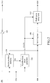
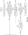
- FIGs. 1A and 1B are schematic architectural views illustrating an application of a serial cluster according to a first embodiment of the present invention.
- a serial controller 100 is applied in the serial cluster 1000, in which the serial cluster 1000 comprises a plurality of serial controllers 100.
- the serial controller 100 of the first embodiment of the present invention can be used for driving LEDs 10 as shown in FIG. 1A or driving stage light controllers (for example, but not limited to, functions similar to DMX 512 controllers) as shown in FIG. 1B , and its application field is not limited thereto.
- the serial cluster 1000 can not only be used for serially connecting and transmitting data signals SDI0, SDI1, SDI2, ..., SDIn to each serial controllers 100, but also converting the data signals transmitted to each serial controllers 100 into pulse width modulation (PWM) signals, or light/dark signals, motor driving signals, and the like for driving the LEDs 10 or the stage lights.
- PWM pulse width modulation
- the serial controller 100 at the 0 th stage of the serial cluster 1000 is connected to the central control unit and receives the data signal SDI0; and the serial controller 100 at the 1 st stage of the serial cluster 1000 is connected to the serial controller 100 at the 0 th stage, and takes the data signal SDI1 output by the serial controller 100 at the 0 th stage as its input data signal.
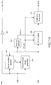
- FIG. 2 is a schematic block view illustrating functions of the serial controller according to the first embodiment of the present invention.
- the serial controller 100 is adapted to receive an external clock CKI and an input data SDI and output an inverted clock CKO and an output data SDO.
- the external clock CKI and the inverted clock CKO in FIG. 2 are respectively corresponding to the clock signals CKI0 and CKI1 in FIG. 1A .
- the input data SDI and the output data SDO in FIG. 2 are respectively corresponding to the data signals SDI0 and SDI1 in FIG. 1A .
- serial controller 100 at the 0 th stage of the serial cluster 1000 is taken as an example for illustration, but the present invention is not limited thereto. That is to say, the serial controller 100 at any stage of the serial cluster 1000 falls within the protection scope of the present invention, and only the serial controller 100 at the 0 th stage is taken as one example for illustration of the embodiment.
- the serial controller 100 comprises an inverter 102, a serial position detector 104, a synchronous clock generator 106, a serial register 108, and a half-cycle delay unit 110.
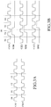
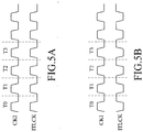
- the inverter 102 receives the external clock CKI and outputs the inverted clock CKO, as shown in FIG. 3A , and the phase of the inverted clock CKO is opposite to the phase of the external clock CKI at any duty cycle T0, T1, T2, T3.
- the external clock CKI is inverted into the inverted clock CKO between any two neighboring stages of the serial cluster 1000, if the phenomenon of uneven duty cycle of the external clock CKI occurs in the transmission process, the phenomenon can be balanced by the serial controller 100 at the next stage.
- the problem of waveform distortion of the external clock CKI caused by the multilevel accumulative effect is solved.
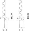
- the serial position detector 104 receives the external clock CKI and the input data SDI and outputs a position signal PS, wherein the position signal PS is an odd signal or an even signal. As shown in FIG. 4A , when the external clock CKI is at a first rising edge RE, and the serial position detector 104 detects that the input data SDI is at the low level, the serial position detector 104 outputs the even signal as the position signal PS. Otherwise, as shown in FIG. 4B , when the external clock CKI is at the first rising edge RE, and the serial position detector 104 detects that the input data SDI is at the high level, the serial position detector 104 outputs the odd signal as the position signal PS.
- the odd signal and the even signal respectively indicate at which stage the serial controller 100 is located within the serial cluster 1000, either at even transmission stage point (the 0 th stage, 2 nd stage, ...) or at odd transmission stage point (the 1 st stage, 3 rd stage, ).
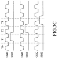
- the synchronous clock generator 106 outputs a synchronous clock ITLCK according to the position signal PS and the external clock CKI. For example, when the position signal PS output by the serial position detector 104 is the odd signal, as shown in FIG. 5A , the synchronous clock ITLCK and the external clock CKI are in the same phase, and when the position signal PS is the even signal, as shown in FIG. 5B , the synchronous clock ITLCK and the external clock CKI are in the opposite phase.
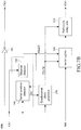
- FIG. 6 is a schematic view illustrating details of the circuit of the serial controller 100 according to the first embodiment of the present invention.
- the synchronous clock generator 106 may comprise a first inverter unit 502 and a selector 504, wherein the first inverter unit 502 receives and inverts the external clock CKI and then outputs an inverted clock of the external clock CKI to the selector 504.
- Two input ends of the selector 504 are respectively connected to the first inverter unit 502 and the external clock CKI, that is, the selector 504 selectively outputs the external clock CKI or the inverted clock of the external clock CKI from the first inverter unit 502.
- the selector 504 when the position signal PS is the odd signal, the selector 504 outputs the external clock CKI as the synchronous clock ITLCK, and when the position signal PS is the even signal, the selector takes the output of the first inverter unit 502 (i.e., the inverted clock of the external clock CKI) as the synchronous clock ITLCK.
- the serial controller 100 is (either at the odd transmission stage point or the even transmission stage point of the serial cluster 1000)
- the synchronous clock generator 106 may still generate a synchronous clock ITLCK that is not limited to the position of the transmission stage point, and thus the synchronous clock ITLCK has 180 degrees of phase difference from the clock received by the serial controller 100 at the 0 th stage (or the even transmission stage point). Thereby, sufficient setup time and hold time are ensured in the data transmission process.
- the serial register 108 receives and temporarily stores the input data SDI according to the synchronous clock ITLCK, and outputs the input data SDI to the half-cycle delay unit 110, so as to complete the data transmission among all stages in the series. Besides, as shown in FIGs.
- the serial register 108 may also buffer the input data SDI stored therein (i.e., to buffer the input data SDI in the serial register 108 to a buffer register) and output the data as the PWM signal, i.e., to convert the data in the buffer register into the PWM signal for driving the LEDs 10 or the light/dark signals, motor driving signals, and the like for driving other electronic components, e.g., driving the stage lights to execute preset functions.
- the output data SDO of the serial controller 100 at each stage may arrive the serial controller 100 at the next stage a half cycle earlier.
- the input data SDI1 is triggered when the clock signal CKI1 is at a falling edge FE of the duty cycle T1, and arrives the serial controller 100 at the 1 st stage a half cycle earlier. Accordingly, if there are numbers of n serial controllers 100 connected in series in the serial cluster 1000, the output data SDO of the serial controller 100 at the n th stage arrives the serial controller 100 at its next stage n/2 cycle earlier.
- the half-cycle delay unit 110 receives the input data SDI from the serial register 108, delays the input data SDI by a half cycle of the synchronous clock ITLCK, and then outputs the data as the output data SDO.
- the half-cycle delay unit 110 comprises a second inverter unit 602 and a register 604.
- the second inverter unit 602 receives and inverts the synchronous clock ITLCK, and then outputs an inverted clock of the synchronous clock ITLCK to the register 604.
- One end of the register 604 receives the input data SDI, and therefore outputs the output data SDO when the inverted clock of the synchronous clock ITLCK is triggered.
- the half-cycle delay unit 110 delays the signal output by the serial register 108 (i.e., the signal received by the half-cycle delay unit 110) by a half cycle of the synchronous clock ITLCK (i.e., the FE is delayed by a half cycle), and in this manner, the output data SDO output by the register 604 and the inverted clock CKO are synchronous, so as to achieve the purpose that the output data SDO of the serial controllers 100 at all stages of the serial cluster 1000 are synchronous with the input data SDI.
- the serial controller 100 at the 1 st stage may receive its input data SDI1 in the duty cycle T2, thus achieving the purpose of synchronous transmission of the serial controllers 100 at all stages.
- serial cluster 1000 since serial transmission is implemented among the serial controllers 100 connected at all stages, and the data signals (the input data SDI and the output data SDO) are delivered one stage to another, the serial controller 100 at each stage needs to identify whether the current data signal is fed to the serial controller 100 at this stage through a decoding mechanism therein.
- the serial cluster 1000 is interfered by noises in long-distance transmission or encounters circumstances like hot-plug, errors may occur to the decoding mechanism of the serial controller 100 and cause chaos.
- the serial controller 100a may further comprise a timeout detector 700 for receiving the external clock CKI, and outputting a reset signal RESET to the serial register 108 when the external clock CKI satisfies such a certain condition that the serial controller 100a can be triggered by the reset signal RESET and resume its decoding mechanism even if the hot-plug or noise interference occurs.
- a timeout detector 700 for receiving the external clock CKI, and outputting a reset signal RESET to the serial register 108 when the external clock CKI satisfies such a certain condition that the serial controller 100a can be triggered by the reset signal RESET and resume its decoding mechanism even if the hot-plug or noise interference occurs.
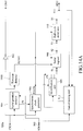
- FIG. 8A is a schematic view of a state machine of the timeout detector 700 according to the second embodiment of the present invention.
- the timeout detector 700 carries out Steps S802, S804, S806, S808, S810, and S812.
- the timeout detector 700 first performs Step S802 and waits for the external clock CKI, and when the external clock CKI is generated, in Step S804, the timeout detector 700 determines whether the time interval between the generated external clock CKI and the previous external clock CKI reaches a first preset time. If yes, in Step S806, the timeout detector 700 continues waiting for the next external clock CKI; otherwise, returns to Step S802 to restart the state machine.
- the timeout detector 700 continues waiting for the next external clock CKI in Step S806, and determines whether the waiting time has reached a second preset time in Step S808. If yes, the timeout detector 700 performs Step S812 to output the reset signal RESET; otherwise, the timeout detector 700 enters Step S810 to determine whether the external clock CKI is generated. If the external clock CKI has already been generated, the timeout detector 700 returns to Step S802 to restart the state machine. If the external clock CKI has not been generated yet, the timeout detector 700 returns to Step S806 to keep waiting.
- FIG. 8B is a relative sequence waveform diagram illustrating the state machine of the timeout detector 700 follows Steps S802, S804, S806, S808, to S812 to output the reset signal RESET
- FIG. 8C illustrates the state machine of the timeout detector 700 follows Steps S802, S804, S806, S808, S810 and returns to Step S802 to restart its state machine (the time interval between two continuous external clocks does not reach the second preset time, and thus the timeout detector 700 follows Steps S808 to S810 and returns to Step S802).
- the first preset time and the second preset time may be respectively preset by the user, e.g., the first preset time may be 100 clock cycles, and the second preset time may be 50 clock cycles and the like.
- FIG. 7B is a schematic block view illustrating functions of a serial controller 100b according to a third embodiment of the present invention.
- the timeout detector 700 and the serial position detector 104 are integrated as a single circuit block to reduce the extra fabricating cost of the circuit and reduce the using area of some chips.
- the serial position detector 104 may determine the position of the serial controller 100 in the serial cluster 1000 through detection of the reset signal RESET and the external clock CKI.
- the serial position detector 104 when the timeout detector 700 generates the reset signal RESET and the serial position detector 104 detects that the external clock CKI is at the high level, the serial position detector 104 outputs the odd signal as the position signal PS. Otherwise, as shown in FIG. 9B , when the timeout detector 700 generates the reset signal RESET and the serial position detector 104 detects that the external clock CKI is at the low level, the serial position detector 104 outputs the even signal as the position signal PS.
- the timeout detector 700 is integrated together within the serial position detector 104 to achieve purpose of a single circuit block, and furthermore a method for determining the position of the serial controller 100 in the serial cluster 1000 according to the reset signal RESET is provided.
- FIGs. 10A and 10B are schematic architectural views illustrating an application of a bi-directional serial cluster according to a fourth embodiment of the present invention.
- a bi-directional serial controller 900 is applied in the bi-directional serial cluster 9000, in which the bi-directional serial cluster 9000 comprises a plurality of bi-directional serial controllers 900.
- the bi-directional serial controller 900 of the fourth embodiment of the present invention can be used for driving LEDs 10 as shown in FIG. 10A or driving stage light controllers (for example, but not limited to, functions similar to DMX 512 controllers) as shown in FIG. 10B , and its application field is not limited thereto.
- the bi-directional serial cluster 9000 can not only be used for serially connecting and bi-directionally transmitting data signals SDI0, SDI1, SDI2, ..., SDIn between the bi-directional serial controllers 900 at all stages, but also converting the data signals SDI0, SDI1, SDI2, ..., SDIn transmitted to the bi-directional serial controllers 900 at all stages into PWM signals, or light/dark signals, motor driving signals, and the like for driving the LEDs 10 or the stage lights.
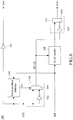
- FIG. 11 is a schematic block view illustrating functions of the bi-directional serial controller 900 according to the fourth embodiment of the present invention.
- the bi-directional serial controller 900 comprises an inverter 902, an input contact 903, a serial position detector 904, a synchronous clock generator 906, a serial register 908, an identification unit 909, a half-cycle delay unit 910, an output contact 911, and a data directing unit 912.
- the inverter 902 receives an external clock CKI and outputs an inverted clock CKO, as shown in FIG. 12 , and the phase of the inverted clock CKO is opposite to the phase of the external clock CKI at any duty cycle T0, T1, T2, T3.
- the input contact 903 receives an input data SDI.
- the serial position detector 904 receives the external clock CKI and the input data SDI and outputs a position signal PS, wherein the position signal PS is an odd signal or an even signal.
- the method for determining whether the position signal PS output by the serial position detector 904 is the odd signal or the even signal is the same as that of the first and second embodiments, i.e. being decided by determining if the input data SDI is at the high or low level when the external clock CKI is at the first rising edge RE.
- the method for determining whether the position of the bi-directional serial controller 900 is located at an odd or even transmission stage point of the bi-directional serial cluster 9000 may also be decided by a reset signal RESET of the bi-directional serial controller 900 (as set forth in the third embodiment).
- the synchronous clock generator 906 outputs a synchronous clock ITLCK according to the position signal PS and the external clock CKI. For example, when the position signal PS output by the serial position detector 904 is the odd signal, the synchronous clock ITLCK and the external clock CKI are in the same phase, and when the position signal PS is the even signal, the synchronous clock ITLCK and the external clock CKI are in the opposite phase.
- FIG. 13 is a schematic view illustrating details of the circuit of the bi-directional serial controller 900 according to the fourth embodiment of the present invention.
- the synchronous clock generator 906 may comprise a first inverter unit 1202 and a selector 1204, in which the first inverter unit 1202 receives and inverts the external clock CKI and then outputs an inverted clock of the external clock CKI to the selector 1204.
- Two input ends of selector 1204 are respectively connected to the first inverter unit 1202 and the external clock CKI, that is, the selector 1204 selectively outputs the external clock CKI or the inverted clock of the external clock CKI from the first inverter unit 1202.
- the selector 1204 when the position signal PS is the odd signal, the selector 1204 outputs the external clock CKI as the synchronous clock ITLCK, and when the position signal PS is the even signal, the selector takes the output of the first inverter unit 1202 (i.e., the inverted clock of the external clock CKI) as the synchronous clock ITLCK.
- the synchronous clock generator 906 may still generate a synchronous clock ITLCK that is not limited to the position of the transmission stage point, and thus the synchronous clock ITLCK has 180 degrees of phase difference from the clock received by the bi-directional serial controller 900 at the 0 th stage (or the even transmission stage point). Thereby, sufficient setup time and hold time are ensured in the data transmission process.
- the serial register 908 has a receiving end 91 and a transmitting end 92, and the serial register 908 temporarily stores signals received by the receiving end 91 according to the synchronous clock ITLCK and outputs the signals from the transmitting end 92. Then, as described in the above embodiment, as shown in FIGs.
- the serial register 908 may also buffer the input data SDI stored therein (i.e., to buffer the input data SDI in the serial register 908 to a buffer register) and output the data as the PWM signal, i.e., to convert the data in the buffer register into the PWM signal for driving the LEDs 10, or the light/dark signals, motor driving signals, and the like for driving other electronic components, e.g., driving the stage lights to execute preset functions.
- the half-cycle delay unit 910 has an input point 93 and an output point 94, wherein the input point 93 is coupled to the transmitting end 92, and the half-cycle delay unit 910 delays the data from the input point 93 by a half cycle of the synchronous clock ITLCK and then outputs the data from the output point 94.
- the half-cycle delay unit 910 may comprise a second inverter unit 1302 and a register 1304.
- the second inverter unit 1302 receives and inverts the synchronous clock ITLCK, and then outputs an inverted clock of the synchronous clock ITLCK to the register 1304.
- One end of the register 1304 is connected to the input point 93, and therefore outputs the signal from the input point 93 to the output point 94 when the inverted clock of the synchronous clock ITLCK is triggered.
- the half-cycle delay unit 910 delays the signal output by the transmitting end 92 (i.e., the signal received by the input point 93) by a half cycle of the synchronous clock ITLCK, and outputs the signal from the output point 94, so as to achieve the purpose that the signal output by the output point 94 is synchronous with the input data SDI.
- the identification unit 909 receives output data of the data directing unit 912 (in an initial state, it is preset to write the data into the transmission point at the next stage, so the output data of the data directing unit 912 is the input data SDI) and the synchronous clock ITLCK, and accordingly outputs a control signal CS.
- the control signal CS comprises a return command, Readmode.
- the input data SDI may contain an information tag, Header, and the identification unit 909 identifies whether the input data SDI is to be transmitted and written into the bi-directional serial controller 900 at the next stage or the state value of the bi-directional serial controller 900 at the current stage is read back by decoding the information tag, Header in the input data SDI.
- the designer when designing the circuit, may selectively integrate the identification unit 909 and the serial register 908 as a single circuit block so as to reduce the extra fabricating cost of the circuit.
- the data directing unit 912 couples the output contact 911 to the receiving end 91 of the serial register 908 (i.e., delivers the signal of the output contact 911 to the receiving end 91), and couples the output point 94 of the half-cycle delay unit 910 to the input contact 903, so as to synchronously return the signal of the output contact 911 to the input contact 903.
- the data directing unit 912 When the data directing unit 912 does not receive the return command, Readmode, the data directing unit 912 couples the input contact 903 to the receiving end 91 of the serial register 908 and couples the output point 94 of the half-cycle delay unit 910 to the output contact 911, so as to synchronously write the input data SDI of the input contact 903 to the bi-directional serial controller 900 at the next stage of the bi-directional serial cluster 9000.
- the data directing unit 912 may comprise an input changeover switch (input bi-directional buffer) 142, an output changeover switch (output bi-directional buffer) 144, and a selector 146.
- the input changeover switch 142 has a first end 41, a second end 42, and a third end 43, in which the first end 41 is coupled to the input contact 903.
- the output changeover switch 144 has a first pin 51, a second pin 52, and a third pin 53, in which the first pin 51 is coupled to the output contact 911, and the third pin 53 is coupled to the output point 94 and the third end 43.
- the selector 146 has a first input end 61, a second input end 62, and an output end 63, in which the first input end 61 is coupled to the second pin 52, the second input end 62 is coupled to the second end 42, and the output end 63 is coupled to the receiving end 91.
- the input changeover switch 142 couples the first end 41 to the third end 43
- the output changeover switch 144 couples the first pin 51 to the second pin 52
- the selector 146 couples the first input end 61 to the output end 63, so as to synchronously return the signal of the first pin 51 (i.e., the output contact 911) to the first end 41 (i.e., the input contact 903).
- the input changeover switch 142 couples the first end 41 to the second end 42
- the output changeover switch 144 couples the first pin 51 to the third pin 53
- the selector 146 couples the second input end 62 to the output end 63, so as to synchronously write the signal of the first end 41 (i.e., the input contact 903) to the first pin 51 (i.e., the output contact 911), to serve as the input data SDI of the bi-directional serial controller 900 at the next stage of the bi-directional serial cluster 9000.
- the bi-directional serial controller 900a may further comprise a timeout detector 1500 for receiving the external clock CKI, and outputting a reset signal RESET to the serial register 908 when the external clock CKI satisfies such a certain condition that the bi-directional serial controller 900a can be triggered by the reset signal RESET and resume its decoding mechanism even if the hot-plug or noise interference occurs.
- the schematic views of the state machine of the timeout detector 1500 are the same as those of the timeout detector 700 in the second and third embodiments, and the details will not be repeated herein.
- the timeout detector 1500 may be selectively integrated together within the serial position detector 904 to achieve a single circuit block.
- the serial position detector 904 may determine whether the position of the bi-directional serial controller 900 is located at the odd or even transmission stage point of the bi-directional serial cluster 9000 through detection of the reset signal RESET and the external clock CKI, and the determination method is the same as that of the third embodiment of the present invention, so the details will not be repeated herein.
- the serial controllers 100 at all stages are connected in series to form the serial cluster 1000, and the synchronous clock generator 106 may generate a synchronous clock ITLCK that is not associated with the transmission stage point of the serial controller 100. Further, the serial controller 100 may use the half-cycle delay unit 110 to achieve the purpose of synchronous transmission of the data signals of the serial controllers 100 at all stages in the long-distance series.
- the bi-directional serial controller 900 of the fourth embodiment of the present invention the purpose of bi-directional transmission of the data signals between the bi-directional serial controllers 900 at all stages is further achieved, such that when the bi-directional serial controller 900 works abnormally, the error detection efficiency of the bi-directional serial cluster 9000 is improved.
Landscapes
- Information Transfer Systems (AREA)
- Dc Digital Transmission (AREA)
Priority Applications (1)
| Application Number | Priority Date | Filing Date | Title |
|---|---|---|---|
| PL10189052T PL2408267T3 (pl) | 2010-07-16 | 2010-10-27 | Sterownik szeregowy i dwukierunkowy sterownik szeregowy dla świateł LED |
Applications Claiming Priority (1)
| Application Number | Priority Date | Filing Date | Title |
|---|---|---|---|
| TW099123578A TWI414207B (zh) | 2010-07-16 | 2010-07-16 | 串列控制器與串列雙向控制器 |
Publications (2)
| Publication Number | Publication Date |
|---|---|
| EP2408267A1 EP2408267A1 (en) | 2012-01-18 |
| EP2408267B1 true EP2408267B1 (en) | 2017-01-25 |
Family
ID=44883540
Family Applications (1)
| Application Number | Title | Priority Date | Filing Date |
|---|---|---|---|
| EP10189052.3A Active EP2408267B1 (en) | 2010-07-16 | 2010-10-27 | Serial controller and bi-directional serial controller for LED lights |
Country Status (6)
| Country | Link |
|---|---|
| US (1) | US8321714B2 (pl) |
| EP (1) | EP2408267B1 (pl) |
| JP (1) | JP5225355B2 (pl) |
| KR (1) | KR101172193B1 (pl) |
| PL (1) | PL2408267T3 (pl) |
| TW (1) | TWI414207B (pl) |
Families Citing this family (31)
| Publication number | Priority date | Publication date | Assignee | Title |
|---|---|---|---|---|
| US7716510B2 (en) | 2006-12-19 | 2010-05-11 | Micron Technology, Inc. | Timing synchronization circuit with loop counter |
| US7656745B2 (en) | 2007-03-15 | 2010-02-02 | Micron Technology, Inc. | Circuit, system and method for controlling read latency |
| US8984320B2 (en) | 2011-03-29 | 2015-03-17 | Micron Technology, Inc. | Command paths, apparatuses and methods for providing a command to a data block |
| CN102568381A (zh) * | 2012-01-19 | 2012-07-11 | 开源集成电路(苏州)有限公司 | Led单元板、led显示屏及信号传输方法 |
| US8552776B2 (en) | 2012-02-01 | 2013-10-08 | Micron Technology, Inc. | Apparatuses and methods for altering a forward path delay of a signal path |
| US9166579B2 (en) * | 2012-06-01 | 2015-10-20 | Micron Technology, Inc. | Methods and apparatuses for shifting data signals to match command signal delay |
| US9054675B2 (en) | 2012-06-22 | 2015-06-09 | Micron Technology, Inc. | Apparatuses and methods for adjusting a minimum forward path delay of a signal path |
| US9001594B2 (en) | 2012-07-06 | 2015-04-07 | Micron Technology, Inc. | Apparatuses and methods for adjusting a path delay of a command path |
| US9329623B2 (en) | 2012-08-22 | 2016-05-03 | Micron Technology, Inc. | Apparatuses, integrated circuits, and methods for synchronizing data signals with a command signal |
| US8913448B2 (en) | 2012-10-25 | 2014-12-16 | Micron Technology, Inc. | Apparatuses and methods for capturing data in a memory |
| TWI496505B (zh) * | 2013-05-28 | 2015-08-11 | Richtek Technology Corp | 發光元件控制電路與其中之熱插拔感知電路及相關發光元件電路 |
| US9508417B2 (en) | 2014-02-20 | 2016-11-29 | Micron Technology, Inc. | Methods and apparatuses for controlling timing paths and latency based on a loop delay |
| US9530473B2 (en) | 2014-05-22 | 2016-12-27 | Micron Technology, Inc. | Apparatuses and methods for timing provision of a command to input circuitry |
| US9531363B2 (en) | 2015-04-28 | 2016-12-27 | Micron Technology, Inc. | Methods and apparatuses including command latency control circuit |
| US9813067B2 (en) | 2015-06-10 | 2017-11-07 | Micron Technology, Inc. | Clock signal and supply voltage variation tracking |
| CN105243968A (zh) * | 2015-10-15 | 2016-01-13 | 利亚德光电股份有限公司 | Led显示器、led电视以及通讯方法和装置 |
| US9865317B2 (en) | 2016-04-26 | 2018-01-09 | Micron Technology, Inc. | Methods and apparatuses including command delay adjustment circuit |
| US9601170B1 (en) | 2016-04-26 | 2017-03-21 | Micron Technology, Inc. | Apparatuses and methods for adjusting a delay of a command signal path |
| CN105848371B (zh) * | 2016-06-20 | 2017-09-15 | 福州台江区超人电子有限公司 | 家居免布线的led灯饰控制器 |
| US9997220B2 (en) | 2016-08-22 | 2018-06-12 | Micron Technology, Inc. | Apparatuses and methods for adjusting delay of command signal path |
| US10224938B2 (en) | 2017-07-26 | 2019-03-05 | Micron Technology, Inc. | Apparatuses and methods for indirectly detecting phase variations |
| CN212486839U (zh) * | 2019-08-13 | 2021-02-05 | 联咏科技股份有限公司 | 发光二极管驱动装置与发光二极管驱动器 |
| US11170702B2 (en) * | 2019-08-13 | 2021-11-09 | Novatek Microelectronics Corp. | Light-emitting diode driving apparatus and light-emitting diode driver |
| CN110996461B (zh) * | 2019-12-30 | 2021-03-02 | 南京浣轩半导体有限公司 | 一种单线led数据传输显示方法及驱动芯片 |
| CN111511062A (zh) * | 2020-06-15 | 2020-08-07 | 大峡谷照明系统(苏州)股份有限公司 | 灯具、灯具控制系统及方法 |
| CN114974140B (zh) * | 2022-05-27 | 2023-08-29 | 北京芯格诺微电子有限公司 | 用于制造Mini-LED背光模组中单线链式通信链路的LED驱动芯片 |
| TWI814511B (zh) * | 2022-08-02 | 2023-09-01 | 明陽半導體股份有限公司 | 具有改良同步機制的裝置串接系統及方法 |
| CN116416929B (zh) * | 2023-06-09 | 2023-09-26 | 中科(深圳)无线半导体有限公司 | 一种led显示系统数据回传控制方法 |
| CN118158023B (zh) * | 2024-05-09 | 2024-07-05 | 深圳三铭电气有限公司 | 一种总线模块信号采集控制方法、装置、设备及存储介质 |
| CN119207294B (zh) * | 2024-10-28 | 2025-08-08 | 北京芯格诺微电子有限公司 | Led驱动系统及驱动方法 |
| CN120032597A (zh) * | 2025-02-21 | 2025-05-23 | 北京显芯科技有限公司 | 背光驱动器、背光单元、背光控制器和显示装置 |
Citations (2)
| Publication number | Priority date | Publication date | Assignee | Title |
|---|---|---|---|---|
| US20030142053A1 (en) * | 2002-01-29 | 2003-07-31 | Fujitsu Limited | Integrated circuit free from accumulation of duty ratio errors |
| US20030218588A1 (en) * | 2002-05-24 | 2003-11-27 | Fujitsu Limited | Semiconductor device, display device, and signal transmission system |
Family Cites Families (28)
| Publication number | Priority date | Publication date | Assignee | Title |
|---|---|---|---|---|
| JPS62246200A (ja) * | 1986-04-18 | 1987-10-27 | Fuji Photo Film Co Ltd | シフトレジスタ |
| JPS62245872A (ja) * | 1986-04-18 | 1987-10-27 | Fuji Photo Film Co Ltd | 固体撮像装置 |
| US5371880A (en) * | 1992-05-13 | 1994-12-06 | Opti, Inc. | Bus synchronization apparatus and method |
| US5706485A (en) * | 1993-09-21 | 1998-01-06 | Intel Corporation | Method and apparatus for synchronizing clock signals in a multiple die circuit including a stop clock feature |
| US5481563A (en) * | 1994-03-14 | 1996-01-02 | Network Systems Corporation | Jitter measurement using a statistically locked loop |
| US5574896A (en) * | 1994-11-04 | 1996-11-12 | National Semiconductor Corporation | Framing circuit that increases the pulse width of the byte clock signal after the byte clock signal is reset |
| KR100212152B1 (ko) * | 1996-12-16 | 1999-08-02 | 윤종용 | 공중파 방송의 데이터 검출회로 |
| US6463109B1 (en) * | 1998-08-25 | 2002-10-08 | Vitesse Semiconductor Corporation | Multiple channel adaptive data recovery system |
| JP3522628B2 (ja) * | 1999-11-09 | 2004-04-26 | シャープ株式会社 | 半導体装置および表示装置モジュール |
| JP4016605B2 (ja) * | 2001-04-12 | 2007-12-05 | セイコーエプソン株式会社 | シフトレジスタ、電気光学装置、駆動回路および電子機器 |
| JP2003295836A (ja) * | 2002-03-29 | 2003-10-15 | Fujitsu Display Technologies Corp | 液晶表示装置及びそのドライバ |
| JP2004260669A (ja) * | 2003-02-27 | 2004-09-16 | Leader Electronics Corp | シリアル・デジタル信号に内在するタイミング基準ビット列に同期するワード・クロック発生器 |
| JP4339317B2 (ja) * | 2003-07-31 | 2009-10-07 | 株式会社アドバンテスト | クロック乗換装置、及び試験装置 |
| CA2521973C (en) * | 2004-09-29 | 2013-12-10 | Tir Systems Ltd. | System and method for controlling luminaires |
| US7328299B2 (en) * | 2004-11-23 | 2008-02-05 | Atmel Corporation | Interface for compressed data transfer between host system and parallel data processing system |
| JP4541131B2 (ja) * | 2004-12-24 | 2010-09-08 | 株式会社沖データ | 駆動回路及びledアレイ駆動回路、並びに駆動回路用配線基板、印刷ヘッド、及び印刷装置 |
| JP3991052B2 (ja) | 2005-02-18 | 2007-10-17 | キヤノン株式会社 | 通信装置及びその通信制御方法 |
| US7331688B2 (en) * | 2005-04-29 | 2008-02-19 | Semisilicon Technology Corp. | Synchronous light emitting diode lamp string |
| US20060294275A1 (en) * | 2005-06-23 | 2006-12-28 | Emil Lambrache | Fast two wire interface and protocol for transferring data |
| CN101233790B (zh) * | 2005-07-27 | 2012-04-11 | 皇家飞利浦电子股份有限公司 | 照明系统和用于控制多个光源的方法 |
| JP4963898B2 (ja) * | 2006-08-11 | 2012-06-27 | 株式会社沖データ | 駆動装置、ledヘッド、及び画像形成装置 |
| EP1965608B1 (en) * | 2007-02-27 | 2015-03-25 | Silicon Touch Technology, Inc. | Control circuit for automatically generating latch signal to control LED device according to input data signal and clock signal |
| US8135011B2 (en) * | 2007-06-07 | 2012-03-13 | Macroblock, Inc. | Method for operating multipoint control system |
| US8400061B2 (en) * | 2007-07-17 | 2013-03-19 | I/O Controls Corporation | Control network for LED-based lighting system in a transit vehicle |
| WO2009095867A2 (en) * | 2008-01-30 | 2009-08-06 | Nxp B.V. | String of light modules |
| US20090323875A1 (en) * | 2008-06-30 | 2009-12-31 | International Business Machines Corporation | Method for Data Synchronization |
| JP5098984B2 (ja) * | 2008-12-10 | 2012-12-12 | 富士通セミコンダクター株式会社 | インターフェース装置及び再同期化方法 |
| KR100902032B1 (ko) | 2009-03-06 | 2009-06-15 | 주식회사 누리플랜 | 라인형 엘이디 조명등의 점등제어장치 |
-
2010
- 2010-07-16 TW TW099123578A patent/TWI414207B/zh active
- 2010-10-20 US US12/908,625 patent/US8321714B2/en active Active
- 2010-10-20 JP JP2010235642A patent/JP5225355B2/ja active Active
- 2010-10-27 EP EP10189052.3A patent/EP2408267B1/en active Active
- 2010-10-27 PL PL10189052T patent/PL2408267T3/pl unknown
- 2010-10-28 KR KR1020100106148A patent/KR101172193B1/ko active Active
Patent Citations (2)
| Publication number | Priority date | Publication date | Assignee | Title |
|---|---|---|---|---|
| US20030142053A1 (en) * | 2002-01-29 | 2003-07-31 | Fujitsu Limited | Integrated circuit free from accumulation of duty ratio errors |
| US20030218588A1 (en) * | 2002-05-24 | 2003-11-27 | Fujitsu Limited | Semiconductor device, display device, and signal transmission system |
Also Published As
| Publication number | Publication date |
|---|---|
| JP2012022665A (ja) | 2012-02-02 |
| US8321714B2 (en) | 2012-11-27 |
| PL2408267T3 (pl) | 2017-07-31 |
| TWI414207B (zh) | 2013-11-01 |
| JP5225355B2 (ja) | 2013-07-03 |
| KR20120008424A (ko) | 2012-01-30 |
| EP2408267A1 (en) | 2012-01-18 |
| TW201206241A (en) | 2012-02-01 |
| KR101172193B1 (ko) | 2012-08-07 |
| US20120017108A1 (en) | 2012-01-19 |
Similar Documents
| Publication | Publication Date | Title |
|---|---|---|
| EP2408267B1 (en) | Serial controller and bi-directional serial controller for LED lights | |
| US9812059B2 (en) | Display device, method for transmitting data packet, and LED system | |
| US8324824B2 (en) | 1-wire communication protocol and interface circuit | |
| US20090289578A1 (en) | Parallel type single-wire addressable lighting device | |
| US9747872B2 (en) | LED display device and method for operating the same | |
| CN104064150A (zh) | 一种led驱动芯片双通道信号传输方法 | |
| CN102044216A (zh) | 一种led显示系统和led驱动电路 | |
| CN203910234U (zh) | Led电源控制电路 | |
| US9953581B2 (en) | Pulse width modulation (PWM) driving scheme and bezel reduction | |
| CN103971642A (zh) | Led显示屏驱动方法及led电源控制电路 | |
| CN103943069A (zh) | Led灯板、led显示屏控制卡以及led显示屏系统 | |
| CN103500542A (zh) | Led灯板 | |
| CN102573184B (zh) | 灯具控制芯片、装置、系统与其寻址方法 | |
| CN113838414B (zh) | 一种支持断点续传的Mini-LED背光驱动控制芯片和系统 | |
| CN109219196A (zh) | 双输入串行级联的防反接电路及应用该电路的led灯条 | |
| CN102340909B (zh) | 串行控制器与串行双向控制器 | |
| CN201159407Y (zh) | 一种新型led数码柔性灯带 | |
| US20100172247A1 (en) | Serial transmission apparatus and the method thereof | |
| CN101996584A (zh) | 多晶片设定地址的方法与结构以及应用的显示系统 | |
| CN107635306B (zh) | 一种基于led控制系统的解码装置和一种led控制系统 | |
| CN104252820A (zh) | 一种s形led显示屏及其连接件 | |
| CN201491318U (zh) | 二线制led驱动电路以及led驱动系统 | |
| CN110706674A (zh) | 时钟恢复装置和源极驱动器 | |
| CN110880289A (zh) | 一种led显示屏及其控制系统 | |
| CN203950532U (zh) | 一种led数码管显示及按键控制芯片 |
Legal Events
| Date | Code | Title | Description |
|---|---|---|---|
| AK | Designated contracting states |
Kind code of ref document: A1 Designated state(s): AL AT BE BG CH CY CZ DE DK EE ES FI FR GB GR HR HU IE IS IT LI LT LU LV MC MK MT NL NO PL PT RO RS SE SI SK SM TR |
|
| AX | Request for extension of the european patent |
Extension state: BA ME |
|
| PUAI | Public reference made under article 153(3) epc to a published international application that has entered the european phase |
Free format text: ORIGINAL CODE: 0009012 |
|
| 17P | Request for examination filed |
Effective date: 20120216 |
|
| 17Q | First examination report despatched |
Effective date: 20120615 |
|
| GRAP | Despatch of communication of intention to grant a patent |
Free format text: ORIGINAL CODE: EPIDOSNIGR1 |
|
| INTG | Intention to grant announced |
Effective date: 20160901 |
|
| GRAS | Grant fee paid |
Free format text: ORIGINAL CODE: EPIDOSNIGR3 |
|
| GRAA | (expected) grant |
Free format text: ORIGINAL CODE: 0009210 |
|
| AK | Designated contracting states |
Kind code of ref document: B1 Designated state(s): AL AT BE BG CH CY CZ DE DK EE ES FI FR GB GR HR HU IE IS IT LI LT LU LV MC MK MT NL NO PL PT RO RS SE SI SK SM TR |
|
| REG | Reference to a national code |
Ref country code: GB Ref legal event code: FG4D |
|
| REG | Reference to a national code |
Ref country code: CH Ref legal event code: EP |
|
| REG | Reference to a national code |
Ref country code: AT Ref legal event code: REF Ref document number: 864772 Country of ref document: AT Kind code of ref document: T Effective date: 20170215 |
|
| REG | Reference to a national code |
Ref country code: IE Ref legal event code: FG4D |
|
| REG | Reference to a national code |
Ref country code: DE Ref legal event code: R096 Ref document number: 602010039760 Country of ref document: DE |
|
| REG | Reference to a national code |
Ref country code: LT Ref legal event code: MG4D |
|
| REG | Reference to a national code |
Ref country code: NL Ref legal event code: MP Effective date: 20170125 |
|
| REG | Reference to a national code |
Ref country code: AT Ref legal event code: MK05 Ref document number: 864772 Country of ref document: AT Kind code of ref document: T Effective date: 20170125 |
|
| PG25 | Lapsed in a contracting state [announced via postgrant information from national office to epo] |
Ref country code: NL Free format text: LAPSE BECAUSE OF FAILURE TO SUBMIT A TRANSLATION OF THE DESCRIPTION OR TO PAY THE FEE WITHIN THE PRESCRIBED TIME-LIMIT Effective date: 20170125 |
|
| PG25 | Lapsed in a contracting state [announced via postgrant information from national office to epo] |
Ref country code: GR Free format text: LAPSE BECAUSE OF FAILURE TO SUBMIT A TRANSLATION OF THE DESCRIPTION OR TO PAY THE FEE WITHIN THE PRESCRIBED TIME-LIMIT Effective date: 20170426 Ref country code: HR Free format text: LAPSE BECAUSE OF FAILURE TO SUBMIT A TRANSLATION OF THE DESCRIPTION OR TO PAY THE FEE WITHIN THE PRESCRIBED TIME-LIMIT Effective date: 20170125 Ref country code: IS Free format text: LAPSE BECAUSE OF FAILURE TO SUBMIT A TRANSLATION OF THE DESCRIPTION OR TO PAY THE FEE WITHIN THE PRESCRIBED TIME-LIMIT Effective date: 20170525 Ref country code: LT Free format text: LAPSE BECAUSE OF FAILURE TO SUBMIT A TRANSLATION OF THE DESCRIPTION OR TO PAY THE FEE WITHIN THE PRESCRIBED TIME-LIMIT Effective date: 20170125 Ref country code: NO Free format text: LAPSE BECAUSE OF FAILURE TO SUBMIT A TRANSLATION OF THE DESCRIPTION OR TO PAY THE FEE WITHIN THE PRESCRIBED TIME-LIMIT Effective date: 20170425 Ref country code: FI Free format text: LAPSE BECAUSE OF FAILURE TO SUBMIT A TRANSLATION OF THE DESCRIPTION OR TO PAY THE FEE WITHIN THE PRESCRIBED TIME-LIMIT Effective date: 20170125 |
|
| PG25 | Lapsed in a contracting state [announced via postgrant information from national office to epo] |
Ref country code: PT Free format text: LAPSE BECAUSE OF FAILURE TO SUBMIT A TRANSLATION OF THE DESCRIPTION OR TO PAY THE FEE WITHIN THE PRESCRIBED TIME-LIMIT Effective date: 20170525 Ref country code: ES Free format text: LAPSE BECAUSE OF FAILURE TO SUBMIT A TRANSLATION OF THE DESCRIPTION OR TO PAY THE FEE WITHIN THE PRESCRIBED TIME-LIMIT Effective date: 20170125 Ref country code: LV Free format text: LAPSE BECAUSE OF FAILURE TO SUBMIT A TRANSLATION OF THE DESCRIPTION OR TO PAY THE FEE WITHIN THE PRESCRIBED TIME-LIMIT Effective date: 20170125 Ref country code: RS Free format text: LAPSE BECAUSE OF FAILURE TO SUBMIT A TRANSLATION OF THE DESCRIPTION OR TO PAY THE FEE WITHIN THE PRESCRIBED TIME-LIMIT Effective date: 20170125 Ref country code: AT Free format text: LAPSE BECAUSE OF FAILURE TO SUBMIT A TRANSLATION OF THE DESCRIPTION OR TO PAY THE FEE WITHIN THE PRESCRIBED TIME-LIMIT Effective date: 20170125 Ref country code: BG Free format text: LAPSE BECAUSE OF FAILURE TO SUBMIT A TRANSLATION OF THE DESCRIPTION OR TO PAY THE FEE WITHIN THE PRESCRIBED TIME-LIMIT Effective date: 20170425 Ref country code: SE Free format text: LAPSE BECAUSE OF FAILURE TO SUBMIT A TRANSLATION OF THE DESCRIPTION OR TO PAY THE FEE WITHIN THE PRESCRIBED TIME-LIMIT Effective date: 20170125 |
|
| REG | Reference to a national code |
Ref country code: DE Ref legal event code: R097 Ref document number: 602010039760 Country of ref document: DE |
|
| PG25 | Lapsed in a contracting state [announced via postgrant information from national office to epo] |
Ref country code: RO Free format text: LAPSE BECAUSE OF FAILURE TO SUBMIT A TRANSLATION OF THE DESCRIPTION OR TO PAY THE FEE WITHIN THE PRESCRIBED TIME-LIMIT Effective date: 20170125 Ref country code: SK Free format text: LAPSE BECAUSE OF FAILURE TO SUBMIT A TRANSLATION OF THE DESCRIPTION OR TO PAY THE FEE WITHIN THE PRESCRIBED TIME-LIMIT Effective date: 20170125 Ref country code: CZ Free format text: LAPSE BECAUSE OF FAILURE TO SUBMIT A TRANSLATION OF THE DESCRIPTION OR TO PAY THE FEE WITHIN THE PRESCRIBED TIME-LIMIT Effective date: 20170125 Ref country code: EE Free format text: LAPSE BECAUSE OF FAILURE TO SUBMIT A TRANSLATION OF THE DESCRIPTION OR TO PAY THE FEE WITHIN THE PRESCRIBED TIME-LIMIT Effective date: 20170125 |
|
| PG25 | Lapsed in a contracting state [announced via postgrant information from national office to epo] |
Ref country code: SM Free format text: LAPSE BECAUSE OF FAILURE TO SUBMIT A TRANSLATION OF THE DESCRIPTION OR TO PAY THE FEE WITHIN THE PRESCRIBED TIME-LIMIT Effective date: 20170125 Ref country code: DK Free format text: LAPSE BECAUSE OF FAILURE TO SUBMIT A TRANSLATION OF THE DESCRIPTION OR TO PAY THE FEE WITHIN THE PRESCRIBED TIME-LIMIT Effective date: 20170125 |
|
| PLBE | No opposition filed within time limit |
Free format text: ORIGINAL CODE: 0009261 |
|
| STAA | Information on the status of an ep patent application or granted ep patent |
Free format text: STATUS: NO OPPOSITION FILED WITHIN TIME LIMIT |
|
| 26N | No opposition filed |
Effective date: 20171026 |
|
| PG25 | Lapsed in a contracting state [announced via postgrant information from national office to epo] |
Ref country code: SI Free format text: LAPSE BECAUSE OF FAILURE TO SUBMIT A TRANSLATION OF THE DESCRIPTION OR TO PAY THE FEE WITHIN THE PRESCRIBED TIME-LIMIT Effective date: 20170125 |
|
| PG25 | Lapsed in a contracting state [announced via postgrant information from national office to epo] |
Ref country code: MC Free format text: LAPSE BECAUSE OF FAILURE TO SUBMIT A TRANSLATION OF THE DESCRIPTION OR TO PAY THE FEE WITHIN THE PRESCRIBED TIME-LIMIT Effective date: 20170125 |
|
| REG | Reference to a national code |
Ref country code: CH Ref legal event code: PL |
|
| GBPC | Gb: european patent ceased through non-payment of renewal fee |
Effective date: 20171027 |
|
| REG | Reference to a national code |
Ref country code: IE Ref legal event code: MM4A |
|
| REG | Reference to a national code |
Ref country code: FR Ref legal event code: ST Effective date: 20180629 |
|
| PG25 | Lapsed in a contracting state [announced via postgrant information from national office to epo] |
Ref country code: CH Free format text: LAPSE BECAUSE OF NON-PAYMENT OF DUE FEES Effective date: 20171031 Ref country code: GB Free format text: LAPSE BECAUSE OF NON-PAYMENT OF DUE FEES Effective date: 20171027 Ref country code: LI Free format text: LAPSE BECAUSE OF NON-PAYMENT OF DUE FEES Effective date: 20171031 Ref country code: LU Free format text: LAPSE BECAUSE OF NON-PAYMENT OF DUE FEES Effective date: 20171027 |
|
| PG25 | Lapsed in a contracting state [announced via postgrant information from national office to epo] |
Ref country code: FR Free format text: LAPSE BECAUSE OF NON-PAYMENT OF DUE FEES Effective date: 20171031 |
|
| PG25 | Lapsed in a contracting state [announced via postgrant information from national office to epo] |
Ref country code: MT Free format text: LAPSE BECAUSE OF NON-PAYMENT OF DUE FEES Effective date: 20171027 |
|
| PG25 | Lapsed in a contracting state [announced via postgrant information from national office to epo] |
Ref country code: IE Free format text: LAPSE BECAUSE OF NON-PAYMENT OF DUE FEES Effective date: 20171027 |
|
| PG25 | Lapsed in a contracting state [announced via postgrant information from national office to epo] |
Ref country code: HU Free format text: LAPSE BECAUSE OF FAILURE TO SUBMIT A TRANSLATION OF THE DESCRIPTION OR TO PAY THE FEE WITHIN THE PRESCRIBED TIME-LIMIT; INVALID AB INITIO Effective date: 20101027 |
|
| PG25 | Lapsed in a contracting state [announced via postgrant information from national office to epo] |
Ref country code: CY Free format text: LAPSE BECAUSE OF NON-PAYMENT OF DUE FEES Effective date: 20170125 |
|
| REG | Reference to a national code |
Ref country code: DE Ref legal event code: R079 Ref document number: 602010039760 Country of ref document: DE Free format text: PREVIOUS MAIN CLASS: H05B0033080000 Ipc: H05B0045000000 |
|
| PG25 | Lapsed in a contracting state [announced via postgrant information from national office to epo] |
Ref country code: MK Free format text: LAPSE BECAUSE OF FAILURE TO SUBMIT A TRANSLATION OF THE DESCRIPTION OR TO PAY THE FEE WITHIN THE PRESCRIBED TIME-LIMIT Effective date: 20170125 |
|
| PG25 | Lapsed in a contracting state [announced via postgrant information from national office to epo] |
Ref country code: TR Free format text: LAPSE BECAUSE OF FAILURE TO SUBMIT A TRANSLATION OF THE DESCRIPTION OR TO PAY THE FEE WITHIN THE PRESCRIBED TIME-LIMIT Effective date: 20170125 |
|
| PG25 | Lapsed in a contracting state [announced via postgrant information from national office to epo] |
Ref country code: AL Free format text: LAPSE BECAUSE OF FAILURE TO SUBMIT A TRANSLATION OF THE DESCRIPTION OR TO PAY THE FEE WITHIN THE PRESCRIBED TIME-LIMIT Effective date: 20170125 |
|
| P01 | Opt-out of the competence of the unified patent court (upc) registered |
Effective date: 20230601 |
|
| PGFP | Annual fee paid to national office [announced via postgrant information from national office to epo] |
Ref country code: DE Payment date: 20240904 Year of fee payment: 15 |
|
| PGFP | Annual fee paid to national office [announced via postgrant information from national office to epo] |
Ref country code: PL Payment date: 20250924 Year of fee payment: 16 Ref country code: IT Payment date: 20250926 Year of fee payment: 16 |
|
| PGFP | Annual fee paid to national office [announced via postgrant information from national office to epo] |
Ref country code: BE Payment date: 20250917 Year of fee payment: 16 |