EP2403079B1 - Reflective semiconductor optical amplifier for optical networks - Google Patents
Reflective semiconductor optical amplifier for optical networks Download PDFInfo
- Publication number
- EP2403079B1 EP2403079B1 EP10290362.2A EP10290362A EP2403079B1 EP 2403079 B1 EP2403079 B1 EP 2403079B1 EP 10290362 A EP10290362 A EP 10290362A EP 2403079 B1 EP2403079 B1 EP 2403079B1
- Authority
- EP
- European Patent Office
- Prior art keywords
- wavelength
- active material
- light
- reflector
- optical
- Prior art date
- Legal status (The legal status is an assumption and is not a legal conclusion. Google has not performed a legal analysis and makes no representation as to the accuracy of the status listed.)
- Active
Links
- 230000003287 optical effect Effects 0.000 title claims description 74
- 239000004065 semiconductor Substances 0.000 title description 14
- 239000011149 active material Substances 0.000 claims description 98
- 230000003321 amplification Effects 0.000 claims description 17
- 238000003199 nucleic acid amplification method Methods 0.000 claims description 17
- 238000000034 method Methods 0.000 claims description 8
- GYHNNYVSQQEPJS-UHFFFAOYSA-N Gallium Chemical compound [Ga] GYHNNYVSQQEPJS-UHFFFAOYSA-N 0.000 claims description 4
- 229910052733 gallium Inorganic materials 0.000 claims description 4
- 229910052738 indium Inorganic materials 0.000 claims description 4
- APFVFJFRJDLVQX-UHFFFAOYSA-N indium atom Chemical compound [In] APFVFJFRJDLVQX-UHFFFAOYSA-N 0.000 claims description 4
- 238000005086 pumping Methods 0.000 claims description 2
- 238000011144 upstream manufacturing Methods 0.000 description 22
- 239000000835 fiber Substances 0.000 description 11
- 230000005540 biological transmission Effects 0.000 description 9
- 239000000463 material Substances 0.000 description 9
- 238000002310 reflectometry Methods 0.000 description 8
- 230000008929 regeneration Effects 0.000 description 6
- 238000011069 regeneration method Methods 0.000 description 6
- 238000010521 absorption reaction Methods 0.000 description 5
- 238000004891 communication Methods 0.000 description 5
- VYPSYNLAJGMNEJ-UHFFFAOYSA-N Silicium dioxide Chemical compound O=[Si]=O VYPSYNLAJGMNEJ-UHFFFAOYSA-N 0.000 description 4
- 239000013307 optical fiber Substances 0.000 description 4
- GWEVSGVZZGPLCZ-UHFFFAOYSA-N Titan oxide Chemical compound O=[Ti]=O GWEVSGVZZGPLCZ-UHFFFAOYSA-N 0.000 description 2
- 229910052782 aluminium Inorganic materials 0.000 description 2
- XAGFODPZIPBFFR-UHFFFAOYSA-N aluminium Chemical compound [Al] XAGFODPZIPBFFR-UHFFFAOYSA-N 0.000 description 2
- 229910052681 coesite Inorganic materials 0.000 description 2
- 229910052906 cristobalite Inorganic materials 0.000 description 2
- 238000010586 diagram Methods 0.000 description 2
- 229910052751 metal Inorganic materials 0.000 description 2
- 239000002184 metal Substances 0.000 description 2
- 239000000203 mixture Substances 0.000 description 2
- 239000000377 silicon dioxide Substances 0.000 description 2
- 229910052709 silver Inorganic materials 0.000 description 2
- 239000004332 silver Substances 0.000 description 2
- 229910052682 stishovite Inorganic materials 0.000 description 2
- 229910052905 tridymite Inorganic materials 0.000 description 2
- 239000000969 carrier Substances 0.000 description 1
- 239000011248 coating agent Substances 0.000 description 1
- 238000000576 coating method Methods 0.000 description 1
- 230000008878 coupling Effects 0.000 description 1
- 238000010168 coupling process Methods 0.000 description 1
- 238000005859 coupling reaction Methods 0.000 description 1
- 230000000694 effects Effects 0.000 description 1
- 239000000284 extract Substances 0.000 description 1
- 150000002739 metals Chemical class 0.000 description 1
- 230000010287 polarization Effects 0.000 description 1
- 230000035945 sensitivity Effects 0.000 description 1
- 235000012239 silicon dioxide Nutrition 0.000 description 1
- 238000001228 spectrum Methods 0.000 description 1
Images

Classifications
-
- G—PHYSICS
- G02—OPTICS
- G02B—OPTICAL ELEMENTS, SYSTEMS OR APPARATUS
- G02B6/00—Light guides; Structural details of arrangements comprising light guides and other optical elements, e.g. couplings
- G02B6/10—Light guides; Structural details of arrangements comprising light guides and other optical elements, e.g. couplings of the optical waveguide type
- G02B6/12—Light guides; Structural details of arrangements comprising light guides and other optical elements, e.g. couplings of the optical waveguide type of the integrated circuit kind
-
- H—ELECTRICITY
- H04—ELECTRIC COMMUNICATION TECHNIQUE
- H04B—TRANSMISSION
- H04B10/00—Transmission systems employing electromagnetic waves other than radio-waves, e.g. infrared, visible or ultraviolet light, or employing corpuscular radiation, e.g. quantum communication
- H04B10/29—Repeaters
- H04B10/291—Repeaters in which processing or amplification is carried out without conversion of the main signal from optical form
- H04B10/297—Bidirectional amplification
- H04B10/2971—A single amplifier for both directions
-
- H—ELECTRICITY
- H01—ELECTRIC ELEMENTS
- H01S—DEVICES USING THE PROCESS OF LIGHT AMPLIFICATION BY STIMULATED EMISSION OF RADIATION [LASER] TO AMPLIFY OR GENERATE LIGHT; DEVICES USING STIMULATED EMISSION OF ELECTROMAGNETIC RADIATION IN WAVE RANGES OTHER THAN OPTICAL
- H01S5/00—Semiconductor lasers
- H01S5/02—Structural details or components not essential to laser action
- H01S5/026—Monolithically integrated components, e.g. waveguides, monitoring photo-detectors, drivers
-
- H—ELECTRICITY
- H01—ELECTRIC ELEMENTS
- H01S—DEVICES USING THE PROCESS OF LIGHT AMPLIFICATION BY STIMULATED EMISSION OF RADIATION [LASER] TO AMPLIFY OR GENERATE LIGHT; DEVICES USING STIMULATED EMISSION OF ELECTROMAGNETIC RADIATION IN WAVE RANGES OTHER THAN OPTICAL
- H01S5/00—Semiconductor lasers
- H01S5/04—Processes or apparatus for excitation, e.g. pumping, e.g. by electron beams
- H01S5/042—Electrical excitation ; Circuits therefor
-
- H—ELECTRICITY
- H01—ELECTRIC ELEMENTS
- H01S—DEVICES USING THE PROCESS OF LIGHT AMPLIFICATION BY STIMULATED EMISSION OF RADIATION [LASER] TO AMPLIFY OR GENERATE LIGHT; DEVICES USING STIMULATED EMISSION OF ELECTROMAGNETIC RADIATION IN WAVE RANGES OTHER THAN OPTICAL
- H01S5/00—Semiconductor lasers
- H01S5/10—Construction or shape of the optical resonator, e.g. extended or external cavity, coupled cavities, bent-guide, varying width, thickness or composition of the active region
-
- H—ELECTRICITY
- H01—ELECTRIC ELEMENTS
- H01S—DEVICES USING THE PROCESS OF LIGHT AMPLIFICATION BY STIMULATED EMISSION OF RADIATION [LASER] TO AMPLIFY OR GENERATE LIGHT; DEVICES USING STIMULATED EMISSION OF ELECTROMAGNETIC RADIATION IN WAVE RANGES OTHER THAN OPTICAL
- H01S5/00—Semiconductor lasers
- H01S5/50—Amplifier structures not provided for in groups H01S5/02 - H01S5/30
- H01S5/5027—Concatenated amplifiers, i.e. amplifiers in series or cascaded
-
- H—ELECTRICITY
- H04—ELECTRIC COMMUNICATION TECHNIQUE
- H04B—TRANSMISSION
- H04B10/00—Transmission systems employing electromagnetic waves other than radio-waves, e.g. infrared, visible or ultraviolet light, or employing corpuscular radiation, e.g. quantum communication
- H04B10/29—Repeaters
- H04B10/291—Repeaters in which processing or amplification is carried out without conversion of the main signal from optical form
-
- H—ELECTRICITY
- H01—ELECTRIC ELEMENTS
- H01S—DEVICES USING THE PROCESS OF LIGHT AMPLIFICATION BY STIMULATED EMISSION OF RADIATION [LASER] TO AMPLIFY OR GENERATE LIGHT; DEVICES USING STIMULATED EMISSION OF ELECTROMAGNETIC RADIATION IN WAVE RANGES OTHER THAN OPTICAL
- H01S3/00—Lasers, i.e. devices using stimulated emission of electromagnetic radiation in the infrared, visible or ultraviolet wave range
- H01S3/23—Arrangements of two or more lasers not provided for in groups H01S3/02 - H01S3/22, e.g. tandem arrangements of separate active media
- H01S3/2308—Amplifier arrangements, e.g. MOPA
- H01S3/2325—Multi-pass amplifiers, e.g. regenerative amplifiers
- H01S3/2333—Double-pass amplifiers
-
- H—ELECTRICITY
- H01—ELECTRIC ELEMENTS
- H01S—DEVICES USING THE PROCESS OF LIGHT AMPLIFICATION BY STIMULATED EMISSION OF RADIATION [LASER] TO AMPLIFY OR GENERATE LIGHT; DEVICES USING STIMULATED EMISSION OF ELECTROMAGNETIC RADIATION IN WAVE RANGES OTHER THAN OPTICAL
- H01S5/00—Semiconductor lasers
- H01S5/02—Structural details or components not essential to laser action
- H01S5/028—Coatings ; Treatment of the laser facets, e.g. etching, passivation layers or reflecting layers
-
- H—ELECTRICITY
- H01—ELECTRIC ELEMENTS
- H01S—DEVICES USING THE PROCESS OF LIGHT AMPLIFICATION BY STIMULATED EMISSION OF RADIATION [LASER] TO AMPLIFY OR GENERATE LIGHT; DEVICES USING STIMULATED EMISSION OF ELECTROMAGNETIC RADIATION IN WAVE RANGES OTHER THAN OPTICAL
- H01S5/00—Semiconductor lasers
- H01S5/10—Construction or shape of the optical resonator, e.g. extended or external cavity, coupled cavities, bent-guide, varying width, thickness or composition of the active region
- H01S5/1003—Waveguide having a modified shape along the axis, e.g. branched, curved, tapered, voids
- H01S5/1017—Waveguide having a void for insertion of materials to change optical properties
Definitions
- the present document relates to passive optical networks (PON). More particularly but not exclusively, it relates to the use of a reflective semiconductor optical amplifier (RSOA) for amplifying signals in a Gigabit PON (GPON) or WDM-PON.
- RSOA reflective semiconductor optical amplifier
- PON is a point-to-multipoint, "fiber to the premises” network architecture in which unpowered passive optical splitters may be used to enable a single optical fiber to serve multiple premises, typically 32 up to 128.
- a PON typically comprises an Optical Line Termination (OLT) at the service provider's central office and a number of Optical Network Units (ONUs) or Optical Network Terminals (ONT) near end users.
- OLT Optical Line Termination
- ONUs Optical Network Units
- ONT Optical Network Terminals
- a PON configuration typically reduces the amount of fiber and central office equipment required compared with point-to-point (PTP) architectures.
- Downstream signals in PON are typically broadcast to each premise sharing a single feeder fiber.
- Upstream signals are typically combined using a Multiple Access Control (MAC) protocol based on Time Division Multiple Access (TDMA).
- the OLTs typically configure the served ONTs in order to provide time slot assignments for upstream communication.
- MAC Multiple Access Control
- TDMA Time Division Multiple Access
- APON Advanced Passive Optical Network
- BPON Broadband PON
- WDM optical channel
- OMCI a standard management interface
- GPON which is an evolution of the BPON standard, supports higher rates, enhanced security, and the choice of the Layer 2 protocol (ATM, TDM and Ethernet via GEM).
- the IEEE issued an Ethernet PON (EPON or GEPON) standard in 2004, as part of the Ethernet First Mile project.
- EPON typically uses standard Ethernet frames with symmetric 1 gigabit per second upstream and downstream rates.
- the ITU-T G.984 GPON standard represents a boost in both the total bandwidth and bandwidth efficiency through the use of large, variable-length packets.
- the standard permits several choices of bit rate, but the industry has converged on 2,488 megabits per second (Mbit/s) of downstream bandwidth, and 1,244 Mbit/s of upstream bandwidth. To allow such bandwidth over a distance of 20 km when using a 64-way optical splitter, a demanding optical budget of 28 dB is required.
- GPON takes advantage of Wavelength Division Multiplexing (WDM), using one wavelength for downstream traffic and another for upstream traffic on a single standard single-mode fiber (ITU-T G.652).
- WDM Wavelength Division Multiplexing
- the specification calls for downstream traffic to be transmitted on the 1490 ( ⁇ 10) nanometer (nm) wavelength and upstream traffic to be transmitted at 1310 ( ⁇ 50) nm wavelength.
- the 1550nm band is allocated for optional overlay services, typically RF video (in the range 1550-1560nm).
- GPON is a shared network, in that the OLT sends a single stream of downstream traffic that is received by all ONTs. Each ONT typically only reads the content of those packets that are addressed to it. Encryption is typically used to prevent eavesdropping on downstream traffic.
- a wavelength of about 1310nm is referred to by the rounded value of 1.3 ⁇ m and a wavelength of about 1490nm wavelength is referred to by the rounded value of 1.5 ⁇ m for the sake of simplicity.
- the present document relates to extending the reach of PON or WDM-PON systems using two or more different optical wavelengths for the downstream and the upstream direction.
- the present document relates to providing an extension of the optical budget in optical access networks. This budget extension should be achieved in a cost-effective manner. Furthermore, the budget extension should be transparent to the underlying optical signals.
- US patent application number 2010/0158427 relates to an optical amplifier in a passive waveguide region and an active waveguide region.
- the passive waveguide region is configured to receive an incident optical signal and adjust a mode of the optical signal.
- the active waveguide region is integrated to the passive waveguide region and configured to perform gain modulation on the optical signal received from the passive waveguide region by changing density of carriers in response to a current applied to the active waveguide region. Internal loss of the active waveguide region is adjusted to produce a resonance effect and thereby to increase bandwidth of the active waveguide. Therefore, the optical amplifier can have a wide bandwidth under a low-current condition.
- an apparatus which is configured to amplify light at different wavelengths in an optical communication network, e.g. a GPON, WDM-PON or WDM network.
- the apparatus may comprise a first active material configured to amplify light at a first wavelength.
- the apparatus may comprise a second active material configured to amplify light at a second wavelength.
- the light within the apparatus may be confined within or carried by an optical waveguide which comprises a first region comprising the first active material and a second region comprising the second active material.
- the optical waveguide may comprise a first end and a second end.
- the light may enter the waveguide at the first end which, relative to the direction of propagation of the entering light, is upstream of the first region.
- the second end of the waveguide is opposite to the first end.
- the apparatus may further comprise a first reflector which separates the first and second active materials and which is configured to reflect light at the first wavelength.
- the first reflector may be configured to be substantially transparent to light at the second wavelength so that light at the second wavelength may be amplified in the second active material.
- the light at different wavelengths may enter the waveguide of the apparatus at a first end.
- the light at the first and second wavelength may be carried through the first region of the waveguide comprising the first active material.
- the light at the first wavelength may be reflected using a first reflector, while the light at the second wavelengths may pass through the reflector to enter the second region of the waveguide comprising the second active material.
- the apparatus may further comprise a second reflector which is provided adjacent the second active material and opposite to the first reflector and which is configured to reflect the light at the second wavelength. Consequently, the light at the second wavelength may be reflected at the opposite end of the second region and carried back to the first end of the waveguide via the second region, the first reflector, and the first region.
- the second reflector may be provided at a second end of the waveguide, opposite to the first end.
- the apparatus may be implemented as a semiconductor optical amplifier comprising active materials which may be semiconducting materials.
- the first active material and/or the second active material may comprise Gallium, Indium, Arsenide and/or Phosphide.
- the second reflector may be provided by the second end of the waveguide of the apparatus. As such, the abrupt end of the waveguide and the abrupt change in refractive index may lead to a reflection of light at specific wavelengths, e.g. light at the second wavelength.
- the second reflector may be implemented by coating the second end of the waveguide with one or more layers of reflective material, e.g. a metal such as Silver or Aluminum.
- the first reflector may comprise an air gap between the first and second active material.
- it is the change in the refractive index between the first active material and the air, as well as the change in the refractive index between the air and the second active material, which provides for a high reflectivity with regards to light at a specific wavelength, e.g. light at the first wavelength, and which provides for a high transparency with regards to light at another wavelength, e.g. light at the second wavelength.
- the reflection and transparency properties of the first reflector with regards to light at different wavelengths may be tuned by adjusting the width of the air gap.
- the air gap between the first and second active material may have a width of about 0.8 ⁇ m which provides for a high reflectivity with regards to a wavelength of about 1.3 ⁇ m and a high transparency with regards to a wavelength of about 1.5 ⁇ m.
- the first reflector may be provided in the form of a Bragg reflector between the first and second active material. This is advantageous as it allows for a reflector with high reflectivity over a narrow wavelength interval and high transparency over another different wavelength interval.
- the first reflector may also be provided by the change in the refractive index which occurs as light propagates from the first active material to the second active material. In this case both active materials may abut on one another.
- the light at the first wavelength may enter the first active material in a direction of propagation which points towards the first reflector and which is substantially perpendicular to the first reflector. Consequently, the direction of propagation of light which travels towards the first reflector and the direction of propagation of reflected light which travels away from the first reflector is substantially parallel.
- the light is carried by the waveguide of the apparatus, wherein the waveguide extends in a direction perpendicular to the first reflector.
- the light at the second wavelength may enter the second active material in a direction of propagation which points towards the second reflector and which is perpendicular to the second reflector so that the light of the second wavelength can be reflected back directly into the waveguide.
- the first and second reflector are substantially parallel so that when the light at the first and second wavelengths is substantially parallel, the direction of propagation of the light at the first wavelength and the direction of propagation of light at the second wavelength are substantially parallel before and after being reflected by the first and second reflector, respectively.
- this is achieved by providing a waveguide for carrying the light at different wavelengths, wherein the waveguide extends within the apparatus in a direction perpendicular to the first and second reflector.
- the apparatus may further comprise means for electrically pumping the first and second active material.
- the apparatus may be used to amplify light at a plurality of wavelengths, i.e. light at two or more different wavelengths.
- the apparatus may be used to amplify light of WDM communication systems using two or more different optical wavelengths.
- the apparatus may be provided with additional active materials and reflectors. If, for example, three different wavelengths are used, the apparatus may further comprise a third active material configured to amplify light at a third wavelength and a third reflector adjacent the third active material opposite to the second reflector which is configured to reflect light at the third wavelength.
- the second reflector may separate the second and the third active materials and may be configured to reflect light at the second wavelength and configured to be substantially transparent to light at the third wavelength.
- the first reflector may be configured to be substantially transparent to light at the third wavelength.
- an apparatus for amplifying light at a plurality of wavelengths comprises a waveguide to carry the light at a plurality of wavelengths.
- the light enters the waveguide of the apparatus at a first end of the waveguide.
- the waveguide comprises a plurality of regions which comprise a plurality of different active materials, respectively. The different regions may be separated by a plurality of reflectors. Each active material may be configured to amplify light at a particular wavelength of the plurality of wavelengths.
- the regions comprising the active materials are arranged such that for each pair of adjacent regions, the active material of the region which is closer to the first end of the waveguide amplifies light at a lower wavelength, compared to the active material of the region which is further away from the first end of the waveguide.
- a reflector between two adjacent regions is typically configured to reflect light at the wavelength of the material amplified within the region which is closer to the first end. Furthermore, the reflector is typically configured to be transparent to light at the wavelengths of the plurality of wavelengths which are greater than the wavelength of the reflected light.
- an optical network comprising a first transmitter/receiver means, a second transmitter/receiver means and amplification means according to any of the above described embodiments.
- the first and second transmitter/receiver means may e.g. be an ONU or an OLT in a GPON or WDM-PON network.
- the first and second transmitter/receiver means may be a WDM transmitter and/or receiver or a WDM transmission network.
- the amplification means may be a semiconductor optical amplifier as described in the present document.
- the first transmitter/receiver means may be connected to the second transmitter/receiver means via the amplification means, thereby extending the optical budget of the optical communication network.
- a method for amplifying light at different wavelengths in an optical network may be based on guiding light at a first and a second wavelength, e.g. within a waveguide, into a first active material wherein the light enters the first active material at a first end of the first active material.
- the light at the first wavelength may then be amplified using the first active material and reflected back into the waveguide at another end of the first active material opposite of the first end of the first active material.
- the light at the second wavelength By guiding the light at the second wavelength through the first active material into the second active material, the light may enter the second active material at a first end of the second active material.
- the light at the second wavelength may be amplified and reflected back into the waveguide by a reflector which is provided at another end of the second active material opposite of the first end of the second active material.
- RSOA reflective SOA
- downstream signals are emitted at about 1.49 ⁇ m in today's GPON access networks. Standardization of the next generation of 10Gbit/s access networks is ongoing, and downstream signals will most likely be located in the wavelength interval of about [1.57 ⁇ m, 1.6 ⁇ m]. Upstream signals will very likely be emitted in the wavelength interval of about [1.26 ⁇ m, 1.3 ⁇ m].
- OEO regeneration In order to perform budget extension in a PON network, Optical-Electronic-Optical (OEO) regeneration may be used.
- the fundamental principle of OEO regeneration is to convert an optical signal into electronic format. Subsequently, the timing and shape of the transmitted signal are restored in the electrical domain. Eventually, the regenerated electrical signal is used to modulate an optical emitter in order to generate a regenerated optical signal.
- Budget extension based on OEO regeneration requires at least a photodiode, a stage of electronic regeneration and an optical emitter for each wavelength.
- OEO regeneration is typically designed for a specific bit-rate. Accordingly, OEO regeneration is inefficient in that it requires at least 3 components per wavelength and it is not transparent to the wavelength and the bit-rate of the transmitted optical signal.
- budget extension in a PON with a fixed set of wavelengths may be performed by semiconductor optical amplifiers (SOA).
- SOA semiconductor optical amplifiers
- each SOA uses a semiconductor which acts as an electrically pumped gain medium.
- GPON transmits an upstream and a downstream signal using different wavelengths.
- two SOAs are required for amplifying the upstream and the downstream signal transmitted in GPON.
- typically a separate SOA is required for each wavelength of the optical WDM system.
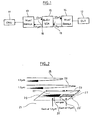
- Fig.1 illustrates a schematic view of an example signal amplifier using two SOAs for the amplification of upstream and downstream data signals in GPON.
- an ONU 11 is connected to an OLT 12 over a first multiplexer/demultiplexer 13, a bi-directional SOA 15 and a second multiplexer/demultiplexer 14.
- the optical signals between the ONU 11 to the OLT 12 are split/merged by the multiplexers/demultiplexers 13, 14 into the different wavelengths of the WDM system, i.e. 1.3 ⁇ m and 1.5 ⁇ m in the illustrated example.
- the upstream signal at 1.3 ⁇ m is de-multiplexed from the fiber 16 coming from ONU 11 using the demultiplexer 13.
- the upstream signal is multiplexed onto the fiber 17 to the OLT 12 using the multiplexer 14.
- de-multiplexer 14 extracts the optical downstream signal at 1.5 ⁇ m from fiber 17, which after passing through the bi-directional SOA 15 is multiplexed onto the fiber 16 to the ONU 11.
- each optical signal corresponding to a specific wavelength is amplified by a specific corresponding SOA, i.e. the 1.3 ⁇ m upstream signal is amplified by a first SOA and the 1.5 ⁇ m downstream signal is amplified by a second SOA.
- the amplifier arrangement of Fig. 1 may be used to amplify both wavelengths in a GPON system, regardless the bit-rate of the signals carried over the different wavelengths.
- the use of a bi-directional SOA 15 is inefficient since it requires a perfect alignment of four fibers, two multiplexer/demultiplexer units 13, 14 and two SOAs.
- the use of two separate SOAs for each wavelength within the bi-directional SOA 15 is typically required because both wavelengths, i.e. 1.3 ⁇ m and 1.5 ⁇ m, are too far apart to be amplified by the same active material of an SOA.
- Such active material is typically limited to amplifying optical signals within a wavelength window of 50nm to 80nm only. If the wavelengths of the upstream and downstream signal, i.e. 1.3 ⁇ m and 1.5 ⁇ m, are to be amplified in a joint amplifier, a conventional semiconductor optical amplifier cannot be used.
- Fig. 2 schematically illustrates an apparatus 21 for amplifying light of different wavelengths, i.e. notably for amplifying light at wavelengths which cover an interval of more than 80nm.
- the apparatus 21 may be used for amplifying optical signals at different optical wavelengths, wherein the different optical wavelengths lie within different wavelength intervals or windows.
- the apparatus 21 comprises a waveguide 20 which comprises different regions 22, 23.
- the waveguide 20 may comprise a first active material 22' within a first region 22 and a second active material 23' within a second region 23.
- the first 22 and second 23 regions may be separated by a first reflector 24.
- the first reflector 24 may reflect the light of a first signal 25 at a wavelength lying within a first wavelength interval.
- the first reflector 24 may be configured to reflect light from the first wavelength interval.
- the first signal 25 has a wavelength of 1.3 ⁇ m lying within the first wavelength interval, e.g. [1.26 ⁇ m, 1.34 ⁇ m].
- the first signal 25 may be the upstream signal in a GPON system.
- a high percentage, e.g. a percentage of more than 50 %, of light of a second signal 26 having a wavelength which lies within a second wavelength interval may pass through the first reflector 24.
- the second wavelength interval is different from the first wavelength interval.
- the second wavelength interval may comprise wavelengths which are larger than the wavelengths of the first wavelength interval.
- all wavelengths of the second wavelength interval pass through the first reflector 24.
- the second wavelength may be 1.5 ⁇ m and the second wavelength interval may be e.g. [1.46 ⁇ m, 1.54 ⁇ m].
- the second signal 26 may be the downstream signal of a GPON system.
- the light of the second wavelength interval and/or the wavelength of the second signal 26 may be reflected by a second reflector 27 which is adjacent the second active material 23, opposite to the first reflector 24.
- the light of the first and second signals 25, 26 may enter the apparatus 21, i.e. the waveguide 20 of the apparatus 21, in a direction towards the first reflector 24, in particular in a direction perpendicular to the plane of the first reflector 24.
- the first reflector 24 and the second reflector 27 may have parallel reflection surfaces.
- the apparatus 21 may be used to separate a first signal 25 from a second signal 26 using a selective reflector 24, wherein the first 25 and second signal 26 have different optical wavelengths within different wavelength intervals. Due to the selective reflector 24, only the second signal 26 enters the second region 23 comprising the second active material 23'.
- the second active material 23' may be selected to amplify light in the second wavelength interval, i.e. to amplify the second signal 26.
- the first active material 22' may be selected to amplify light in the first wavelength interval, while leaving light in the second wavelength interval unaffected. In other words, the first active material 22' may be selected to amplify the first signal 25, while leaving unaffected the second signal 26.
- opto-electrical materials for the first 22 and second 23 region.
- Such opto-electrical materials may be designed to amplify light within a pre-determined wavelength interval.
- the material may be designed such that light at wavelengths below the pre-determined wavelength interval is absorbed, while light at a wavelength above the pre-determined wavelength interval passes through the opto-electrical material unaffected.
- the first and second active materials 22', 23' may comprise Indium (In), Gallium (Ga), Arsenide (As) and/or Phosphide (P).
- the first active material 22' may be In x Ga (1-x) As y P (1-y) with x-0.71 and y-0.62, in order to amplify light at the first wavelength interval and in particular the wavelength of the first signal 25 (e.g. 1.3 ⁇ m).
- the second active material 23' may be In x Ga (1-x) As y P (1-y) with x-0.58 and y-0.9, in order to amplify light at the second wavelength interval and in particular the wavelength of the second signal 26 (e.g. 1.3 ⁇ m). It should be clear to the skilled person that these values are to be interpreted as approximations, as the exact compositions will typically depend on the strain in the epitaxial layers (in order to optimize the sensitivity to incoming light polarization).
- the reflectors 24, 27 may be implemented by various optical reflection means.
- the first reflector 24, i.e. a reflector between two active materials 22', 23' may be provided by an air gap of a particular width or a Bragg reflector.
- the width (in signal direction) of the air gap and/or the design of the layers of the Bragg reflector are selected such that the first signal 25 is reflected, whereas the second signal 26 is allowed to pass.
- the second reflector 27, i.e. the last reflector of the apparatus 21, may e.g. be provided by the end of a waveguide, i.e. by the abrupt edge of the waveguide. This end or edge may be further provided with at least one reflective layer.
- the at least one reflective layer may comprise layers of Si/SiO 2 or TiO2/SiO2 or metals such as Silver or Aluminum.
- N being an arbitrary integer value greater than one
- T N comprises the highest wavelengths
- T 1 comprises the lowest wavelengths.
- Each reflector R i is configured to reflect wavelengths ⁇ i from the wavelengths interval T i . Furthermore, each reflector R i is configured to let pass wavelengths ⁇ j from the wavelengths interval T j , for j>i.
- Each active material M i is configured to amplify light at a wavelength ⁇ i belonging to the wavelength interval T i . Furthermore, each active material M i is configured to leave unaffected light at a wavelength ⁇ j belonging to the wavelength interval T j , for j>i.
- the above conditions may be achieved by selecting appropriate compositions of opto-electrical materials M i such as semiconductor materials comprising Indium (In), Gallium (Ga), Arsenide (As) and/or Phosphide (P).
- the different reflectors R i may be implemented by designing appropriate Bragg refractors and/or air gap reflectors.
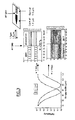
- Fig. 3 illustrates the gain and absorption incurred by signals at two different wavelengths within apparatus 21.
- the gain/absorption table 31 illustrates that the first signal 25 having a wavelength within the first wavelength interval, e.g. the 1.3 ⁇ m signal, may be amplified when passing through the first active material 22' and may be absorbed when passing through the second active material 23'.
- gain/absorption table 32 shows that the second signal 26 having a wavelength within the second wavelength interval, e.g. the 1.5 ⁇ m signal, passes through the first active material 22' without being absorbed and is only lightly reflected by reflector 24.
- 32 only the second signal 26 enters the second region 23, so that the second active material 23' may be selected to amplify the second signal 26.
- the reflector 24 of apparatus 21 may comprise an air gap between the first active material 22' and the second active material 23', the air gap having a width (in the direction of propagation of the signal) of about 0.75 to about 0.85 ⁇ m.
- the air gap may have a width of about 0.8 ⁇ m.
- the width of the air gap may be adjusted, in order to adjust the reflectivity/transparency of the wavelength selective selector 24 to the specific signal wavelengths.
- Fig. 4 illustrates a schematic view of an optical network comprising a first transmitter/receiver 41, e.g. an ONU, a second transmitter/receiver 42, e.g. an OLT, and signal amplification means 21, e.g. apparatus 21 shown in Fig. 2 , i.e. a reflective semiconductor optical amplifier (RSOA).
- a first transmitter/receiver 41 e.g. an ONU
- a second transmitter/receiver 42 e.g. an OLT
- signal amplification means 21 e.g. apparatus 21 shown in Fig. 2
- RSOA reflective semiconductor optical amplifier
- ONU 41 may be connected to RSOA 21 by first data transmission means 43.
- Said first data transmission means may be operable to transmit one or more signals, e.g. light of specific wavelengths.
- the specific wavelengths may be in the 100THz region, i.e. the near-infrared or visible region of the electromagnetic spectrum.
- the data transmission means may be an optical connector such as an optical fiber.
- RSOA 21 may be connected to OLT 42 by second data transmission means 44 which may have the same properties as first data transmission means 43.
- the optical network according to Fig.4 may be a PON, e.g. a WDM-PON and/or GPON.
- RSOA 21 may be the signal amplification means described with reference to Fig. 2 .
- the first and second data transmission means 43, 44 are connected to the waveguide 20 of the RSOA 21. This connection may be performed by butt coupling of the data transmission means 43, 44, e.g. fibers, and the waveguide 20 of RSOA 21.
- a wavelength selective amplifier for optical signals has been described.
- a wavelength selective reflective semiconductor optical amplifier for GPON systems has been described.
- the amplifier may be directly connected to an optical fiber carrying a plurality of wavelengths.
- the need for separate multiplexer/demultiplexer units 13, 14 is removed.
- the amplification of the different optical wavelengths may be performed in a single semiconductor optical amplifier, thereby removing the need for separates SOAs for the different wavelengths and the need for aligning an increased number of optical fibers.
- an efficient and cost-effective solution has been described for amplifying a plurality of optical wavelength within a single semiconductor optical amplifier.
- the optical amplifier may be applied to GPON, 10GPON, WDM-PON access networks or WDM transmission networks.
Landscapes
- Physics & Mathematics (AREA)
- Electromagnetism (AREA)
- General Physics & Mathematics (AREA)
- Optics & Photonics (AREA)
- Condensed Matter Physics & Semiconductors (AREA)
- Engineering & Computer Science (AREA)
- Computer Networks & Wireless Communication (AREA)
- Signal Processing (AREA)
- Microelectronics & Electronic Packaging (AREA)
- Optical Communication System (AREA)
- Semiconductor Lasers (AREA)
- Optical Modulation, Optical Deflection, Nonlinear Optics, Optical Demodulation, Optical Logic Elements (AREA)
Priority Applications (9)
| Application Number | Priority Date | Filing Date | Title |
|---|---|---|---|
| EP10290362.2A EP2403079B1 (en) | 2010-06-30 | 2010-06-30 | Reflective semiconductor optical amplifier for optical networks |
| SG2012089991A SG186215A1 (en) | 2010-06-30 | 2011-06-16 | Reflective semiconductor optical amplifier for optical networks |
| PCT/EP2011/060045 WO2012000804A1 (en) | 2010-06-30 | 2011-06-16 | Reflective semiconductor optical amplifier for optical networks |
| CN201180032578.XA CN102986098B (zh) | 2010-06-30 | 2011-06-16 | 用于光学网络的反射式半导体光学放大器 |
| KR1020127033993A KR101500056B1 (ko) | 2010-06-30 | 2011-06-16 | 광학 네트워크용 반사 반도체 광학 증폭기 |
| JP2013517159A JP5662568B2 (ja) | 2010-06-30 | 2011-06-16 | 光学ネットワークのための反射型半導体光増幅器 |
| US13/698,330 US8948605B2 (en) | 2010-06-30 | 2011-06-16 | Reflective semiconductor optical amplifier for optical networks |
| MYPI2012005072A MY172343A (en) | 2010-06-30 | 2011-06-16 | Reflective semiconductor optical amplifier for optical networks |
| TW100121842A TWI497136B (zh) | 2010-06-30 | 2011-06-22 | 放大光纖網路中不同波長的光之方法、設備及光纖網路 |
Applications Claiming Priority (1)
| Application Number | Priority Date | Filing Date | Title |
|---|---|---|---|
| EP10290362.2A EP2403079B1 (en) | 2010-06-30 | 2010-06-30 | Reflective semiconductor optical amplifier for optical networks |
Publications (2)
| Publication Number | Publication Date |
|---|---|
| EP2403079A1 EP2403079A1 (en) | 2012-01-04 |
| EP2403079B1 true EP2403079B1 (en) | 2014-01-15 |
Family
ID=43020406
Family Applications (1)
| Application Number | Title | Priority Date | Filing Date |
|---|---|---|---|
| EP10290362.2A Active EP2403079B1 (en) | 2010-06-30 | 2010-06-30 | Reflective semiconductor optical amplifier for optical networks |
Country Status (9)
| Country | Link |
|---|---|
| US (1) | US8948605B2 (enExample) |
| EP (1) | EP2403079B1 (enExample) |
| JP (1) | JP5662568B2 (enExample) |
| KR (1) | KR101500056B1 (enExample) |
| CN (1) | CN102986098B (enExample) |
| MY (1) | MY172343A (enExample) |
| SG (1) | SG186215A1 (enExample) |
| TW (1) | TWI497136B (enExample) |
| WO (1) | WO2012000804A1 (enExample) |
Families Citing this family (4)
| Publication number | Priority date | Publication date | Assignee | Title |
|---|---|---|---|---|
| KR102168666B1 (ko) * | 2013-08-26 | 2020-10-21 | (주)승재 | 반사형 반도체 광 증폭기 패키지 |
| KR102168665B1 (ko) * | 2013-08-26 | 2020-10-21 | (주)승재 | 반사형 반도체 광 증폭기가 포함된 수동형 광 네트워크 |
| TWI581401B (zh) * | 2014-06-09 | 2017-05-01 | Chunghwa Telecom Co Ltd | Reflective Semiconductor Optical Amplifier |
| US12451962B2 (en) * | 2020-03-02 | 2025-10-21 | Nec Corporation | Monitoring signal light output apparatus, submarine apparatus, and optical communication system |
Family Cites Families (22)
| Publication number | Priority date | Publication date | Assignee | Title |
|---|---|---|---|---|
| US4794346A (en) * | 1984-11-21 | 1988-12-27 | Bell Communications Research, Inc. | Broadband semiconductor optical amplifier structure |
| JPH0575093A (ja) | 1991-09-13 | 1993-03-26 | Nippon Telegr & Teleph Corp <Ntt> | 光集積回路 |
| JP3149987B2 (ja) | 1992-03-23 | 2001-03-26 | キヤノン株式会社 | 半導体光増幅素子およびその使用法 |
| SE470454B (sv) * | 1992-08-26 | 1994-04-11 | Ericsson Telefon Ab L M | Optisk filteranordning |
| JP4005705B2 (ja) | 1998-07-22 | 2007-11-14 | 日立電線株式会社 | 広帯域半導体光増幅器 |
| JP2000058953A (ja) * | 1998-08-11 | 2000-02-25 | Kdd Corp | 光増幅装置 |
| JP3328881B2 (ja) | 1999-05-26 | 2002-09-30 | 独立行政法人産業技術総合研究所 | 半導体光パルス圧縮導波路素子及び半導体光パルス発生レーザ |
| JP2001156364A (ja) * | 1999-11-29 | 2001-06-08 | Sumitomo Electric Ind Ltd | 広帯域光増幅器 |
| JP2002148733A (ja) | 2000-11-07 | 2002-05-22 | Fuji Photo Film Co Ltd | 放射線画像読取装置 |
| US6757100B2 (en) * | 2001-02-12 | 2004-06-29 | Metrophotonics Inc. | Cascaded semiconductor optical amplifier |
| JP2002280649A (ja) | 2001-03-15 | 2002-09-27 | Nippon Telegr & Teleph Corp <Ntt> | 光の反射体及び光増幅器 |
| JP2003124578A (ja) | 2001-10-09 | 2003-04-25 | Nippon Telegr & Teleph Corp <Ntt> | 半導体光増幅素子 |
| US6788727B2 (en) * | 2002-06-13 | 2004-09-07 | Intel Corporation | Method and apparatus for tunable wavelength conversion using a bragg grating and a laser in a semiconductor substrate |
| US6891878B2 (en) * | 2003-05-01 | 2005-05-10 | Raytheon Company | Eye-safe solid state laser system and method |
| US7095772B1 (en) * | 2003-05-22 | 2006-08-22 | Research Foundation Of The University Of Central Florida, Inc. | Extreme chirped/stretched pulsed amplification and laser |
| US7643758B1 (en) * | 2006-01-04 | 2010-01-05 | Cisco Technology, Inc. | CWDM system architecture with amplification |
| JPWO2007080891A1 (ja) * | 2006-01-11 | 2009-06-11 | 日本電気株式会社 | 半導体レーザ、モジュール、及び、光送信機 |
| US7450848B2 (en) * | 2006-04-28 | 2008-11-11 | Broadway Networks, Ltd, | High-speed fiber-to-the-premise optical communication system |
| KR100842277B1 (ko) | 2006-12-07 | 2008-06-30 | 한국전자통신연구원 | 반사형 반도체 광증폭기 및 수퍼 루미네센스 다이오드 |
| JP2009124046A (ja) | 2007-11-16 | 2009-06-04 | Advanced Telecommunication Research Institute International | 半導体レーザ素子および半導体レーザジャイロ |
| KR100987793B1 (ko) * | 2008-10-10 | 2010-10-13 | 한국전자통신연구원 | 반사형 반도체 광 증폭기 및 이를 이용하는 광신호 처리방법 |
| US8594469B2 (en) * | 2008-12-22 | 2013-11-26 | Electronics And Telecommunications Research Institute | Optical amplifier |
-
2010
- 2010-06-30 EP EP10290362.2A patent/EP2403079B1/en active Active
-
2011
- 2011-06-16 KR KR1020127033993A patent/KR101500056B1/ko not_active Expired - Fee Related
- 2011-06-16 US US13/698,330 patent/US8948605B2/en active Active
- 2011-06-16 CN CN201180032578.XA patent/CN102986098B/zh active Active
- 2011-06-16 JP JP2013517159A patent/JP5662568B2/ja not_active Expired - Fee Related
- 2011-06-16 WO PCT/EP2011/060045 patent/WO2012000804A1/en not_active Ceased
- 2011-06-16 SG SG2012089991A patent/SG186215A1/en unknown
- 2011-06-16 MY MYPI2012005072A patent/MY172343A/en unknown
- 2011-06-22 TW TW100121842A patent/TWI497136B/zh not_active IP Right Cessation
Also Published As
| Publication number | Publication date |
|---|---|
| CN102986098A (zh) | 2013-03-20 |
| JP5662568B2 (ja) | 2015-02-04 |
| MY172343A (en) | 2019-11-21 |
| TW201213910A (en) | 2012-04-01 |
| CN102986098B (zh) | 2014-12-17 |
| JP2013530542A (ja) | 2013-07-25 |
| US8948605B2 (en) | 2015-02-03 |
| US20130101297A1 (en) | 2013-04-25 |
| TWI497136B (zh) | 2015-08-21 |
| KR20130041835A (ko) | 2013-04-25 |
| WO2012000804A1 (en) | 2012-01-05 |
| SG186215A1 (en) | 2013-01-30 |
| EP2403079A1 (en) | 2012-01-04 |
| KR101500056B1 (ko) | 2015-03-06 |
Similar Documents
| Publication | Publication Date | Title |
|---|---|---|
| US8532489B2 (en) | Multi-fiber ten gigabit passive optical network optical line terminal for optical distribution network coexistence with gigabit passive optical network | |
| US7773838B2 (en) | Method and network architecture for upgrading legacy passive optical network to wavelength division multiplexing passive optical network based next-generation passive optical network | |
| US8897639B2 (en) | Methods and systems for increasing reach and/or split in passive optical networks | |
| CN102187601B (zh) | 一种无源光网络系统、耦合器以及方法 | |
| US8774630B2 (en) | Method, apparatus, and system for a self-seeded external cavity laser for dense wavelength division multiplexing applications | |
| CN101399617B (zh) | 局端光通信装置及光通信系统 | |
| US7440701B2 (en) | Fiber-to-the-premise optical communication system | |
| US20100322626A1 (en) | Multiple passive optical network system | |
| US9287987B2 (en) | Self-seeded colorless burst-mode transmitter using reflective semiconductor optical amplifier and injection locked Fabry-Perot laser | |
| Ghoniemy | Enhanced time and wavelength division multiplexed passive optical network (TWDM-PON) for triple-play broadband service delivery in FTTx networks | |
| EP2403079B1 (en) | Reflective semiconductor optical amplifier for optical networks | |
| CN101127571A (zh) | 一种wdm-pon系统共享的公共光源及光源共享的方法 | |
| US9699532B2 (en) | Systems and methods of hybrid DWDM aggregation and extension for time division multiplexing passive optical networks | |
| US9602216B2 (en) | Reflective light-emitting device for a WDM PON optical access network, the device including a light source with an optical gain medium | |
| Huelsermann et al. | Cost and performance evaluation of WDM-based access networks | |
| Sierra et al. | Evaluation of two prevalent EPON networks using simulation methods | |
| Chan et al. | Novel WDM passive optical network with bidirectional protection | |
| Bohara et al. | Optical Networks | |
| Spiekman | Semiconductor optical amplifiers in access networks | |
| KR101062395B1 (ko) | 광증폭기 | |
| KR20050069472A (ko) | 파장 분할 다중화 방식의 수동형 광 가입자망 시스템 |
Legal Events
| Date | Code | Title | Description |
|---|---|---|---|
| AK | Designated contracting states |
Kind code of ref document: A1 Designated state(s): AL AT BE BG CH CY CZ DE DK EE ES FI FR GB GR HR HU IE IS IT LI LT LU LV MC MK MT NL NO PL PT RO SE SI SK SM TR |
|
| AX | Request for extension of the european patent |
Extension state: BA ME RS |
|
| PUAI | Public reference made under article 153(3) epc to a published international application that has entered the european phase |
Free format text: ORIGINAL CODE: 0009012 |
|
| 17P | Request for examination filed |
Effective date: 20120704 |
|
| GRAP | Despatch of communication of intention to grant a patent |
Free format text: ORIGINAL CODE: EPIDOSNIGR1 |
|
| INTG | Intention to grant announced |
Effective date: 20130801 |
|
| RIC1 | Information provided on ipc code assigned before grant |
Ipc: H04B 10/291 20130101ALI20130802BHEP Ipc: H04B 10/2587 20130101ALI20130802BHEP Ipc: G02B 6/12 20060101ALI20130802BHEP Ipc: H01S 5/50 20060101AFI20130802BHEP |
|
| 111Z | Information provided on other rights and legal means of execution |
Free format text: AL AT BE BG CH CY CZ DE DK EE ES FI FR GB GR HR HU IE IS IT LI LT LU LV MC MK MT NL NO PL PT RO SE SI SK SM TR Effective date: 20130410 |
|
| GRAS | Grant fee paid |
Free format text: ORIGINAL CODE: EPIDOSNIGR3 |
|
| GRAA | (expected) grant |
Free format text: ORIGINAL CODE: 0009210 |
|
| AK | Designated contracting states |
Kind code of ref document: B1 Designated state(s): AL AT BE BG CH CY CZ DE DK EE ES FI FR GB GR HR HU IE IS IT LI LT LU LV MC MK MT NL NO PL PT RO SE SI SK SM TR |
|
| REG | Reference to a national code |
Ref country code: GB Ref legal event code: FG4D Ref country code: CH Ref legal event code: EP |
|
| REG | Reference to a national code |
Ref country code: AT Ref legal event code: REF Ref document number: 650178 Country of ref document: AT Kind code of ref document: T Effective date: 20140215 |
|
| REG | Reference to a national code |
Ref country code: IE Ref legal event code: FG4D |
|
| REG | Reference to a national code |
Ref country code: DE Ref legal event code: R096 Ref document number: 602010013117 Country of ref document: DE Effective date: 20140227 |
|
| REG | Reference to a national code |
Ref country code: NL Ref legal event code: VDEP Effective date: 20140115 |
|
| REG | Reference to a national code |
Ref country code: AT Ref legal event code: MK05 Ref document number: 650178 Country of ref document: AT Kind code of ref document: T Effective date: 20140115 |
|
| REG | Reference to a national code |
Ref country code: LT Ref legal event code: MG4D Ref country code: GB Ref legal event code: 732E Free format text: REGISTERED BETWEEN 20140529 AND 20140604 |
|
| PG25 | Lapsed in a contracting state [announced via postgrant information from national office to epo] |
Ref country code: IS Free format text: LAPSE BECAUSE OF FAILURE TO SUBMIT A TRANSLATION OF THE DESCRIPTION OR TO PAY THE FEE WITHIN THE PRESCRIBED TIME-LIMIT Effective date: 20140515 Ref country code: LT Free format text: LAPSE BECAUSE OF FAILURE TO SUBMIT A TRANSLATION OF THE DESCRIPTION OR TO PAY THE FEE WITHIN THE PRESCRIBED TIME-LIMIT Effective date: 20140115 Ref country code: NO Free format text: LAPSE BECAUSE OF FAILURE TO SUBMIT A TRANSLATION OF THE DESCRIPTION OR TO PAY THE FEE WITHIN THE PRESCRIBED TIME-LIMIT Effective date: 20140415 |
|
| REG | Reference to a national code |
Ref country code: CH Ref legal event code: PCOW Free format text: NEW ADDRESS: 148/152 ROUTE DE LA REINE, 92100 BOULOGNE-BILLANCOURT (FR) |
|
| REG | Reference to a national code |
Ref country code: FR Ref legal event code: GC Effective date: 20140602 |
|
| RAP2 | Party data changed (patent owner data changed or rights of a patent transferred) |
Owner name: ALCATEL LUCENT |
|
| PG25 | Lapsed in a contracting state [announced via postgrant information from national office to epo] |
Ref country code: PT Free format text: LAPSE BECAUSE OF FAILURE TO SUBMIT A TRANSLATION OF THE DESCRIPTION OR TO PAY THE FEE WITHIN THE PRESCRIBED TIME-LIMIT Effective date: 20140515 Ref country code: SE Free format text: LAPSE BECAUSE OF FAILURE TO SUBMIT A TRANSLATION OF THE DESCRIPTION OR TO PAY THE FEE WITHIN THE PRESCRIBED TIME-LIMIT Effective date: 20140115 Ref country code: CY Free format text: LAPSE BECAUSE OF FAILURE TO SUBMIT A TRANSLATION OF THE DESCRIPTION OR TO PAY THE FEE WITHIN THE PRESCRIBED TIME-LIMIT Effective date: 20140115 Ref country code: FI Free format text: LAPSE BECAUSE OF FAILURE TO SUBMIT A TRANSLATION OF THE DESCRIPTION OR TO PAY THE FEE WITHIN THE PRESCRIBED TIME-LIMIT Effective date: 20140115 Ref country code: ES Free format text: LAPSE BECAUSE OF FAILURE TO SUBMIT A TRANSLATION OF THE DESCRIPTION OR TO PAY THE FEE WITHIN THE PRESCRIBED TIME-LIMIT Effective date: 20140115 Ref country code: AT Free format text: LAPSE BECAUSE OF FAILURE TO SUBMIT A TRANSLATION OF THE DESCRIPTION OR TO PAY THE FEE WITHIN THE PRESCRIBED TIME-LIMIT Effective date: 20140115 Ref country code: NL Free format text: LAPSE BECAUSE OF FAILURE TO SUBMIT A TRANSLATION OF THE DESCRIPTION OR TO PAY THE FEE WITHIN THE PRESCRIBED TIME-LIMIT Effective date: 20140115 |
|
| PG25 | Lapsed in a contracting state [announced via postgrant information from national office to epo] |
Ref country code: BE Free format text: LAPSE BECAUSE OF FAILURE TO SUBMIT A TRANSLATION OF THE DESCRIPTION OR TO PAY THE FEE WITHIN THE PRESCRIBED TIME-LIMIT Effective date: 20140115 Ref country code: HR Free format text: LAPSE BECAUSE OF FAILURE TO SUBMIT A TRANSLATION OF THE DESCRIPTION OR TO PAY THE FEE WITHIN THE PRESCRIBED TIME-LIMIT Effective date: 20140115 Ref country code: LV Free format text: LAPSE BECAUSE OF FAILURE TO SUBMIT A TRANSLATION OF THE DESCRIPTION OR TO PAY THE FEE WITHIN THE PRESCRIBED TIME-LIMIT Effective date: 20140115 |
|
| REG | Reference to a national code |
Ref country code: DE Ref legal event code: R097 Ref document number: 602010013117 Country of ref document: DE |
|
| PG25 | Lapsed in a contracting state [announced via postgrant information from national office to epo] |
Ref country code: RO Free format text: LAPSE BECAUSE OF FAILURE TO SUBMIT A TRANSLATION OF THE DESCRIPTION OR TO PAY THE FEE WITHIN THE PRESCRIBED TIME-LIMIT Effective date: 20140115 Ref country code: DK Free format text: LAPSE BECAUSE OF FAILURE TO SUBMIT A TRANSLATION OF THE DESCRIPTION OR TO PAY THE FEE WITHIN THE PRESCRIBED TIME-LIMIT Effective date: 20140115 Ref country code: CZ Free format text: LAPSE BECAUSE OF FAILURE TO SUBMIT A TRANSLATION OF THE DESCRIPTION OR TO PAY THE FEE WITHIN THE PRESCRIBED TIME-LIMIT Effective date: 20140115 Ref country code: EE Free format text: LAPSE BECAUSE OF FAILURE TO SUBMIT A TRANSLATION OF THE DESCRIPTION OR TO PAY THE FEE WITHIN THE PRESCRIBED TIME-LIMIT Effective date: 20140115 |
|
| PLBE | No opposition filed within time limit |
Free format text: ORIGINAL CODE: 0009261 |
|
| STAA | Information on the status of an ep patent application or granted ep patent |
Free format text: STATUS: NO OPPOSITION FILED WITHIN TIME LIMIT |
|
| PG25 | Lapsed in a contracting state [announced via postgrant information from national office to epo] |
Ref country code: PL Free format text: LAPSE BECAUSE OF FAILURE TO SUBMIT A TRANSLATION OF THE DESCRIPTION OR TO PAY THE FEE WITHIN THE PRESCRIBED TIME-LIMIT Effective date: 20140115 Ref country code: SK Free format text: LAPSE BECAUSE OF FAILURE TO SUBMIT A TRANSLATION OF THE DESCRIPTION OR TO PAY THE FEE WITHIN THE PRESCRIBED TIME-LIMIT Effective date: 20140115 |
|
| 26N | No opposition filed |
Effective date: 20141016 |
|
| PG25 | Lapsed in a contracting state [announced via postgrant information from national office to epo] |
Ref country code: LU Free format text: LAPSE BECAUSE OF FAILURE TO SUBMIT A TRANSLATION OF THE DESCRIPTION OR TO PAY THE FEE WITHIN THE PRESCRIBED TIME-LIMIT Effective date: 20140630 Ref country code: MC Free format text: LAPSE BECAUSE OF FAILURE TO SUBMIT A TRANSLATION OF THE DESCRIPTION OR TO PAY THE FEE WITHIN THE PRESCRIBED TIME-LIMIT Effective date: 20140115 |
|
| REG | Reference to a national code |
Ref country code: CH Ref legal event code: PL |
|
| REG | Reference to a national code |
Ref country code: DE Ref legal event code: R097 Ref document number: 602010013117 Country of ref document: DE Effective date: 20141016 |
|
| REG | Reference to a national code |
Ref country code: IE Ref legal event code: MM4A |
|
| PG25 | Lapsed in a contracting state [announced via postgrant information from national office to epo] |
Ref country code: IE Free format text: LAPSE BECAUSE OF NON-PAYMENT OF DUE FEES Effective date: 20140630 Ref country code: CH Free format text: LAPSE BECAUSE OF NON-PAYMENT OF DUE FEES Effective date: 20140630 Ref country code: LI Free format text: LAPSE BECAUSE OF NON-PAYMENT OF DUE FEES Effective date: 20140630 |
|
| PG25 | Lapsed in a contracting state [announced via postgrant information from national office to epo] |
Ref country code: SI Free format text: LAPSE BECAUSE OF FAILURE TO SUBMIT A TRANSLATION OF THE DESCRIPTION OR TO PAY THE FEE WITHIN THE PRESCRIBED TIME-LIMIT Effective date: 20140115 |
|
| REG | Reference to a national code |
Ref country code: FR Ref legal event code: PLFP Year of fee payment: 6 |
|
| PG25 | Lapsed in a contracting state [announced via postgrant information from national office to epo] |
Ref country code: MT Free format text: LAPSE BECAUSE OF FAILURE TO SUBMIT A TRANSLATION OF THE DESCRIPTION OR TO PAY THE FEE WITHIN THE PRESCRIBED TIME-LIMIT Effective date: 20140115 |
|
| PG25 | Lapsed in a contracting state [announced via postgrant information from national office to epo] |
Ref country code: SM Free format text: LAPSE BECAUSE OF FAILURE TO SUBMIT A TRANSLATION OF THE DESCRIPTION OR TO PAY THE FEE WITHIN THE PRESCRIBED TIME-LIMIT Effective date: 20140115 |
|
| REG | Reference to a national code |
Ref country code: FR Ref legal event code: PLFP Year of fee payment: 7 |
|
| PG25 | Lapsed in a contracting state [announced via postgrant information from national office to epo] |
Ref country code: BG Free format text: LAPSE BECAUSE OF FAILURE TO SUBMIT A TRANSLATION OF THE DESCRIPTION OR TO PAY THE FEE WITHIN THE PRESCRIBED TIME-LIMIT Effective date: 20140115 Ref country code: GR Free format text: LAPSE BECAUSE OF FAILURE TO SUBMIT A TRANSLATION OF THE DESCRIPTION OR TO PAY THE FEE WITHIN THE PRESCRIBED TIME-LIMIT Effective date: 20140416 Ref country code: IT Free format text: LAPSE BECAUSE OF FAILURE TO SUBMIT A TRANSLATION OF THE DESCRIPTION OR TO PAY THE FEE WITHIN THE PRESCRIBED TIME-LIMIT Effective date: 20140115 |
|
| PG25 | Lapsed in a contracting state [announced via postgrant information from national office to epo] |
Ref country code: TR Free format text: LAPSE BECAUSE OF FAILURE TO SUBMIT A TRANSLATION OF THE DESCRIPTION OR TO PAY THE FEE WITHIN THE PRESCRIBED TIME-LIMIT Effective date: 20140115 Ref country code: HU Free format text: LAPSE BECAUSE OF FAILURE TO SUBMIT A TRANSLATION OF THE DESCRIPTION OR TO PAY THE FEE WITHIN THE PRESCRIBED TIME-LIMIT; INVALID AB INITIO Effective date: 20100630 |
|
| REG | Reference to a national code |
Ref country code: FR Ref legal event code: PLFP Year of fee payment: 8 |
|
| REG | Reference to a national code |
Ref country code: FR Ref legal event code: PLFP Year of fee payment: 9 |
|
| PG25 | Lapsed in a contracting state [announced via postgrant information from national office to epo] |
Ref country code: MK Free format text: LAPSE BECAUSE OF FAILURE TO SUBMIT A TRANSLATION OF THE DESCRIPTION OR TO PAY THE FEE WITHIN THE PRESCRIBED TIME-LIMIT Effective date: 20140115 |
|
| PG25 | Lapsed in a contracting state [announced via postgrant information from national office to epo] |
Ref country code: AL Free format text: LAPSE BECAUSE OF FAILURE TO SUBMIT A TRANSLATION OF THE DESCRIPTION OR TO PAY THE FEE WITHIN THE PRESCRIBED TIME-LIMIT Effective date: 20140115 |
|
| PGFP | Annual fee paid to national office [announced via postgrant information from national office to epo] |
Ref country code: GB Payment date: 20240509 Year of fee payment: 15 |
|
| PGFP | Annual fee paid to national office [announced via postgrant information from national office to epo] |
Ref country code: DE Payment date: 20240507 Year of fee payment: 15 |
|
| PGFP | Annual fee paid to national office [announced via postgrant information from national office to epo] |
Ref country code: FR Payment date: 20240509 Year of fee payment: 15 |