EP2400829A2 - Hochfrequenzvorrichtung und Druckplattenhaltestruktur - Google Patents
Hochfrequenzvorrichtung und Druckplattenhaltestruktur Download PDFInfo
- Publication number
- EP2400829A2 EP2400829A2 EP11168945A EP11168945A EP2400829A2 EP 2400829 A2 EP2400829 A2 EP 2400829A2 EP 11168945 A EP11168945 A EP 11168945A EP 11168945 A EP11168945 A EP 11168945A EP 2400829 A2 EP2400829 A2 EP 2400829A2
- Authority
- EP
- European Patent Office
- Prior art keywords
- printed board
- case
- solder
- projecting part
- high frequency
- Prior art date
- Legal status (The legal status is an assumption and is not a legal conclusion. Google has not performed a legal analysis and makes no representation as to the accuracy of the status listed.)
- Withdrawn
Links
- 229910000679 solder Inorganic materials 0.000 claims abstract description 92
- 239000002184 metal Substances 0.000 claims abstract description 13
- 238000005452 bending Methods 0.000 claims description 5
- 239000006071 cream Substances 0.000 description 26
- 238000000034 method Methods 0.000 description 10
- 239000007788 liquid Substances 0.000 description 9
- 238000005476 soldering Methods 0.000 description 8
- 230000008569 process Effects 0.000 description 7
- 210000000078 claw Anatomy 0.000 description 5
- 230000008901 benefit Effects 0.000 description 3
- 238000010438 heat treatment Methods 0.000 description 3
- 230000000694 effects Effects 0.000 description 2
- 230000007480 spreading Effects 0.000 description 2
- 230000004075 alteration Effects 0.000 description 1
- 230000005484 gravity Effects 0.000 description 1
- 238000002844 melting Methods 0.000 description 1
- 230000008018 melting Effects 0.000 description 1
- 230000008520 organization Effects 0.000 description 1
- 238000003825 pressing Methods 0.000 description 1
- 238000006467 substitution reaction Methods 0.000 description 1
Images


Classifications
-
- H—ELECTRICITY
- H05—ELECTRIC TECHNIQUES NOT OTHERWISE PROVIDED FOR
- H05K—PRINTED CIRCUITS; CASINGS OR CONSTRUCTIONAL DETAILS OF ELECTRIC APPARATUS; MANUFACTURE OF ASSEMBLAGES OF ELECTRICAL COMPONENTS
- H05K9/00—Screening of apparatus or components against electric or magnetic fields
- H05K9/0007—Casings
- H05K9/002—Casings with localised screening
- H05K9/0039—Galvanic coupling of ground layer on printed circuit board [PCB] to conductive casing
-
- H—ELECTRICITY
- H05—ELECTRIC TECHNIQUES NOT OTHERWISE PROVIDED FOR
- H05K—PRINTED CIRCUITS; CASINGS OR CONSTRUCTIONAL DETAILS OF ELECTRIC APPARATUS; MANUFACTURE OF ASSEMBLAGES OF ELECTRICAL COMPONENTS
- H05K7/00—Constructional details common to different types of electric apparatus
- H05K7/14—Mounting supporting structure in casing or on frame or rack
- H05K7/1417—Mounting supporting structure in casing or on frame or rack having securing means for mounting boards, plates or wiring boards
-
- H—ELECTRICITY
- H05—ELECTRIC TECHNIQUES NOT OTHERWISE PROVIDED FOR
- H05K—PRINTED CIRCUITS; CASINGS OR CONSTRUCTIONAL DETAILS OF ELECTRIC APPARATUS; MANUFACTURE OF ASSEMBLAGES OF ELECTRICAL COMPONENTS
- H05K9/00—Screening of apparatus or components against electric or magnetic fields
- H05K9/0007—Casings
- H05K9/006—Casings specially adapted for signal processing applications, e.g. CATV, tuner, antennas amplifier
Definitions
- the present invention generally relates to high frequency devices and printed board holding structures. More specifically, the present invention relates to a high frequency device and a printed board holding structure having a metal case, and a printed board configured to be inserted into the case.
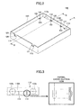
- FIG. 1 is a view for explaining an example where a printed board and a case are fixed to each other.
- FIG. 1(A) shows a state where cream solder 3 is applied between a case 1 and a printed board 2 in order to fill a space H between the case 1 and the printed board 2.
- FIG. 1(B) shows a state where the cream solder is melted by heating in the reflow process in the state shown in FIG. 1(A).
- FIG. 1(C) shows an ideal solder state when the case 1 and the printed board 2 are fixed to each other.
- the frame includes a claw part and a projecting part.
- the claw part extends to an upper or lower part of an end part of a receiving part bent and projecting from a side plate.
- the projecting part projects to an inside.
- the printed board includes a through hole configured to receive the claw part and is received by the projecting part.
- Japanese Laid-Open Patent Application Publication No. 11-121945 describes a structure having a frame having a side plate with end surfaces where at least an upper part is opened.
- the printed board is provided at an internal surface of the side plate situated inside the frame.
- Japanese Laid-Open Patent Application Publication No. 7-122874 describes a structure where a concave part is provided at a metal frame corresponding to both ends of a portion connected to a board.
- embodiments of the present invention may provide a novel and useful high frequency device and a printed board holding structure solving one or more of the problems discussed above.
- the embodiments of the present invention may provide a high frequency device and a printed board holding structure where a printed board and a case can be stably soldered in a simple step in a reflow process and good electric capabilities can be obtained.
- Another aspect of the embodiments of the present invention may be to provide a high frequency device, including a metal case; a printed board configured to be inserted in the case; a projecting part configured to project to an inside of the case; a solder guiding hole formed at the projecting part; a board concave part formed in a position of the printed board, the position corresponding to the projecting part; and a land surface formed on the printed board along an edge of the board concave part, wherein the printed board is provided so that a part of the solder guiding hole is positioned above the land surface when the printed board is inserted in the case.
- Another aspect of the embodiments of the present invention may be to provide a printed board holding structure including a metal case and a printed board configured to be inserted in the case, the printed board holding structure being configured to hold the printed board, the printed board holding structure including a projecting part configured to project to an inside of the case; a solder guiding hole formed at the projecting part; a board concave part formed in a position of the printed board, the position corresponding to the projecting part; and a land surface formed on the printed board along an edge of the board concave part, wherein the printed board is provided so that a part of the solder guiding hole is positioned above the land surface when the printed board is inserted in the case.
- a projecting part is formed at a metal case.
- the projecting part is formed in a body with the case.
- the projecting part is configured to project to an inside of the case.
- a solder guiding hole is formed at a part of the projecting part. The solder is guided from the inside to the outside of the case by the solder guiding part.
- the projecting part is engaged with a concave part of the printed board and soldering is performed in a reflow process.
- FIG. 2 is a perspective view of a high frequency device of an embodiment of the present invention.
- a printed board 120 is fitted into a metal case 110. Opening parts 111a and 111b and notch parts 112 are formed in the case 110.
- the opening parts 111a and 111b are configured to connect a connector.
- the connector is configured to input and output a video signal.
- the notch parts 112 are configured to determine a position where the printed board 120 is fitted in the case 110.
- Various kinds of electronic circuits for performing as the high frequency device 100 are mounted on the printed board 120 (not illustrated in FIG. 2 ).
- claw parts 121 are formed at the printed board 120. By engaging the claw parts 121 with the notch parts 112, a position for fixing the printed board 120 is determined.
- a bottom plate and a lid part are provided at the case 110 so as to cover the printed board 120.
- Projecting parts 113 are formed at the case 110 of the embodiment of the present invention.
- the projecting parts 113 are configured to aid in soldering the printed board 120 and the case 110.
- two of the projecting parts 113 are provided between the opening part 111a and the opening part 111b.
- a single projecting part 113 is provided at each of two side plates perpendicular to a side plate 110A where the opening parts 111a and 111b are formed. Details of a structure of the projecting part 113 are discussed below.
- Concave parts 122 are formed at the printed board 120 of the embodiment of the present invention.
- the projecting parts 113 are engaged with the concave parts 122.
- the concave parts 122 are formed in positions where the projecting parts 113 are engaged when the printed board 120 is fixed to the case 110.
- a land part 123 is formed at the printed board 120 along a periphery of the concave part 122.
- the land part 123 may be formed so as to have, for example, a semicircular-shaped configuration or a configuration of half of an ellipse.
- the land part 123 may have a configuration where a head end of a semicircle is cut in a straight line manner (see FIG. 4(B) ).
- FIG. 3 is a side view of the high frequency device 100 seen in an A direction in FIG. 2 .
- the projecting part 113 may be formed by pressing the side plate 110A of the case 110 from an outside to an inside.
- the projecting part 113 has a bending configuration where the head projects inside to the side plate 110A.
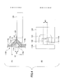
- FIG. 4(A) is a cross-sectional view taken along a line B-B of the high frequency device 100.
- FIG. 4(B) is a top view in a state where the projecting part 113 is engaged with the concave part 122.
- the projecting part 113 of the embodiment of the present invention has a bending configuration where a part of the side plate 110A is pressed to the inside of the case 110.
- an upper end part 113a and a lower end part 113b of the projecting part 113 are not separated from the side plate 110A.
- the projecting part 113 is formed so as to be continuous with the side plate 110A in a Y-Y direction.
- a solder guiding hole 114 is formed in a concave part 113A.
- the concave part 113A is formed at the external circumferential surface of the case 110.
- the solder guiding hole 114 is configured to guide the molten solder to the side of the case 110.
- the printed board 120 is provided so that the distance between the upper end part 113a and the land part 123 on the printed board 120 is H2.
- the distance H2 is approximately 1/2 of the width H1.
- the printed board 120 is provided so that a head end part 113c of the projecting part 113 is positioned on the same plane surface as the land part 123.
- the distance H2 is 1/2 of the width H1.
- the printed board 120 may be provided so that the land part 123 may be positioned in an area of a width H3 of the solder guiding hole 114 in the Y-Y direction.
- a width W1 in the X-X direction of the projecting part 113 of this embodiment is approximately 1 mm. See FIG. 4(B) .
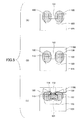
- FIGs. 5(A)-5(C) are views for explaining soldering of the case 110 and the printed board 120 of the embodiment of the present invention.
- cream solder 130 is applied on the land parts 123 of the printed board 120.
- the printed board 120 is inserted into the case 110 as shown in FIG. 5(B) .
- the projecting parts 113 formed at the case 110 are engaged with the corresponding concave parts 122 of the printed wiring board 120.
- the liquid solder flows in the space between the head end of the projecting part 113 and the concave part 122.
- the liquid solder goes to the external circumferential side of the case 110 due to capillarity generated by the solder guiding hole 114 formed at the projecting part 113, so as to flow into the concave part 113A formed at the external circumferential surface of the case 110.
- the capillarity is a phenomenon where liquid situated inside a narrow pipe may go up (against gravity) inside the pipe.
- the liquid solder comes together at a portion where the projecting part 113 and the land part 123 are connected to each other. At the same time, the flow of the liquid solder is spread to right and left uniformly at the internal circumferential surface of the side plate 110A of the case 110, so that a solder surface is formed.
- FIG. 6 is a view for explaining a state where the case 110 and the printed board 120 of the embodiment of the present invention are soldered.
- the concave part 113A of the projecting part 113 is filled with solder G so that the solder guiding hole 114 is blocked by the solder G.
- the printed board 120 and a part of the projecting part 113 situated above the surface of the printed board 120 where the land part 123 is formed, are connected to each other by the solder F having a large area.
- the case 110 and the printed board 120 can be fixed to each other with a large area.
- the part where the case 110 and the printed board 120 are connected to each other can have a stable solder configuration.
- the solder guiding hole 114 is blocked in the soldering step, it is possible to improve the shield effect of the case 110 so that good electric properties can be kept.
- the projecting part 113 is provided in the vicinity of a connector configured to input and output video signals, it is possible to reduce noise or the like of the video signals.
- no opening part is provided at the case 110 after the soldering is completed, it is possible to maintain the strength of the case 110.
- the liquid solder spontaneously spreads between the projecting part 113 and the land part 123 by the capillarity. Therefore, when the cream solder 130 is applied on the land 123, the cream solder may be applied in a position of the solder guiding hole 114. Because of this, in this embodiment, after the cream solder 130 is applied on the land part 123, the printed board 120 can be inserted in the case 110. Therefore, regardless of the configuration of the case 110, it is possible to apply the cream solder by a device having a simple structure.
- the act of guiding the solder to the case 110 of this embodiment is not performed.
- a device having a structure corresponding to the configuration of the case 110 is required. Therefore, large-sized equipment is required and flexibility of the equipment is degraded.
- the printed board 120 can be installed in the case 110. Therefore, it is possible to directly apply the cream solder to the printed board 120. Hence, the cream solder can be applied by simple equipment.
- FIGs. 7(A) and 7(B) are views for explaining application of cream solder.
- FIG. 7(A) is a view for explaining a related art structure where the solder guiding hole 114 is not provided.
- FIG. 7(B) is a view for explaining a structure where the solder guiding hole 114 is provided.
- a cream solder applying pipe 60 for applying the cream solder should have a configuration corresponding to the case.
- the printed board 120 and the case 110 can be stably soldered in a simple step in a reflow process and good electric capabilities (properties) can be obtained.
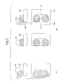
- FIG. 8 is a view showing a first modified example.
- FIG. 9 is a view showing a second modified example.
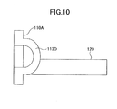
- FIG. 10 is a view showing a third modified example.
- a projecting part 113B does not have the bending configuration but a substantially square-shaped configuration.
- a solder guiding hole 114B is provided at the projecting part 113B shown in FIG. 8 .
- a projecting part 113C is bent at approximately 90 degrees.
- a solder guiding hole 114C is provided at the projecting part 113C shown in FIG. 9 .
- a projecting part 113D has a circular-shaped configuration.
- a solder guiding hole 114D is provided at a projecting part 113D shown in FIG. 10 .
- One aspect of the embodiments of the present invention may be to provide a high frequency device (100), including a metal case (110); a printed board (120) configured to be inserted in the case (110); a projecting part (113) configured to project to an inside of the case (110); a solder guiding hole (114) formed at the projecting part (113); a board concave part (122) formed in a position of the printed board (120), the position corresponding to the projecting part (113); and a land surface (123) formed on the printed board (120) along an edge of the board concave part (122), wherein the printed board (120) is provided so that a part of the solder guiding hole (114) is positioned above the land surface (123) when the printed board (120) is inserted in the case (110).
- the projecting part (113) may be formed so as to be continuous with a side plate in a long side direction or a short side direction of the side plate of the case (110) where the projecting part (113) is formed.
- An upper end part and a lower end part of the projecting part may not be separated from the side plate and the projecting part may be formed so as to be continuous with the side plate.
- the printed board (120) may be provided so that a head end (113c) of the projecting part (113) is positioned on a same plane surface as the land surface (123).
- a case concave part (113A) may be formed at an external circumferential surface of the projecting part (113) along a configuration of the projecting part (113).
- the projecting part (113) may have a bending configuration where a part of the side plate (110A) is pressed to the inside of the case (110).
- the solder guiding hole (114) may be configured to guide solder from an internal circumferential side to an external circumferential side of the case (110), the solder being configured to connect the case (110) and the printed board (120) to each other.
- Another aspect of the embodiments of the present invention may be to provide a printed board holding structure including a metal case (110) and a printed board (120) configured to be inserted in the case (110), the printed board holding structure being configured to hold the printed board (120), the printed board holding structure including: a projecting part (113) configured to project to an inside of the case (110); a solder guiding hole (114) formed at the projecting part (113); a board concave part (122) formed in a position of the printed board (120), the position corresponding to the projecting part (113); and a land surface (123) formed on the printed board (120) along an edge of the board concave part (122), wherein the printed board (120) is provided so that a part of the solder guiding hole (114) is positioned above the land surface (123) when the printed board (120) is inserted in the case (110).
Landscapes
- Engineering & Computer Science (AREA)
- Microelectronics & Electronic Packaging (AREA)
- Signal Processing (AREA)
- Shielding Devices Or Components To Electric Or Magnetic Fields (AREA)
- Mounting Of Printed Circuit Boards And The Like (AREA)
- Combinations Of Printed Boards (AREA)
Applications Claiming Priority (1)
| Application Number | Priority Date | Filing Date | Title |
|---|---|---|---|
| JP2010141223A JP2012009471A (ja) | 2010-06-22 | 2010-06-22 | 高周波装置及びプリント基板保持構造 |
Publications (2)
| Publication Number | Publication Date |
|---|---|
| EP2400829A2 true EP2400829A2 (de) | 2011-12-28 |
| EP2400829A3 EP2400829A3 (de) | 2012-07-25 |
Family
ID=44673965
Family Applications (1)
| Application Number | Title | Priority Date | Filing Date |
|---|---|---|---|
| EP11168945A Withdrawn EP2400829A3 (de) | 2010-06-22 | 2011-06-07 | Hochfrequenzvorrichtung und Druckplattenhaltestruktur |
Country Status (4)
| Country | Link |
|---|---|
| US (1) | US20110310573A1 (de) |
| EP (1) | EP2400829A3 (de) |
| JP (1) | JP2012009471A (de) |
| CN (1) | CN102300447A (de) |
Families Citing this family (3)
| Publication number | Priority date | Publication date | Assignee | Title |
|---|---|---|---|---|
| CN104750217A (zh) * | 2013-12-31 | 2015-07-01 | 鸿富锦精密工业(武汉)有限公司 | 电源 |
| US10772245B2 (en) | 2016-04-04 | 2020-09-08 | Commscope Technologies Llc | Systems and methods for thermal management for high power density EMI shielded electronic devices |
| CN113597160B (zh) * | 2021-07-22 | 2022-12-27 | 业成科技(成都)有限公司 | 外壳边框及电子设备 |
Citations (4)
| Publication number | Priority date | Publication date | Assignee | Title |
|---|---|---|---|---|
| JPH07122874A (ja) | 1993-10-27 | 1995-05-12 | Matsushita Electric Ind Co Ltd | 高周波装置 |
| JPH0856085A (ja) | 1994-08-11 | 1996-02-27 | Alps Electric Co Ltd | プリント基板保持構造 |
| JPH11121945A (ja) | 1997-10-14 | 1999-04-30 | Alps Electric Co Ltd | 電子機器、並びにこの電子機器の製造方法 |
| JP2010141223A (ja) | 2008-12-15 | 2010-06-24 | Hitachi Kokusai Electric Inc | 半導体装置の製造方法及び基板処理装置 |
Family Cites Families (5)
| Publication number | Priority date | Publication date | Assignee | Title |
|---|---|---|---|---|
| JPS60124088A (ja) * | 1983-12-09 | 1985-07-02 | Columbia Magune Prod Kk | カセツトテ−プ自動巻取組立装置 |
| JPS60124088U (ja) * | 1984-01-30 | 1985-08-21 | 関西日本電気株式会社 | プリント配線装置 |
| JPH10107463A (ja) * | 1996-10-02 | 1998-04-24 | Alps Electric Co Ltd | プリント基板の取付構造 |
| JP3267521B2 (ja) * | 1996-11-08 | 2002-03-18 | アルプス電気株式会社 | プリント基板の取付構造 |
| JP2001251070A (ja) * | 2000-03-03 | 2001-09-14 | Sharp Corp | 基板の取付構造 |
-
2010
- 2010-06-22 JP JP2010141223A patent/JP2012009471A/ja active Pending
-
2011
- 2011-05-26 US US13/116,354 patent/US20110310573A1/en not_active Abandoned
- 2011-06-07 EP EP11168945A patent/EP2400829A3/de not_active Withdrawn
- 2011-06-20 CN CN201110175609A patent/CN102300447A/zh active Pending
Patent Citations (4)
| Publication number | Priority date | Publication date | Assignee | Title |
|---|---|---|---|---|
| JPH07122874A (ja) | 1993-10-27 | 1995-05-12 | Matsushita Electric Ind Co Ltd | 高周波装置 |
| JPH0856085A (ja) | 1994-08-11 | 1996-02-27 | Alps Electric Co Ltd | プリント基板保持構造 |
| JPH11121945A (ja) | 1997-10-14 | 1999-04-30 | Alps Electric Co Ltd | 電子機器、並びにこの電子機器の製造方法 |
| JP2010141223A (ja) | 2008-12-15 | 2010-06-24 | Hitachi Kokusai Electric Inc | 半導体装置の製造方法及び基板処理装置 |
Also Published As
| Publication number | Publication date |
|---|---|
| JP2012009471A (ja) | 2012-01-12 |
| US20110310573A1 (en) | 2011-12-22 |
| CN102300447A (zh) | 2011-12-28 |
| EP2400829A3 (de) | 2012-07-25 |
Similar Documents
| Publication | Publication Date | Title |
|---|---|---|
| US9510438B2 (en) | Electronic control device | |
| CN102195256B (zh) | 电气接线盒 | |
| US20160192515A1 (en) | Circuit board assembly and assembling method thereof | |
| JP2022510118A (ja) | レセプタクルコネクタ | |
| KR101011918B1 (ko) | 케이블 어셈블리 | |
| EP2400829A2 (de) | Hochfrequenzvorrichtung und Druckplattenhaltestruktur | |
| CN104078734A (zh) | 高频传输装置 | |
| JP6354594B2 (ja) | 電子装置 | |
| CN210576836U (zh) | 一种屏蔽罩、屏蔽组件及连接器 | |
| KR20150060845A (ko) | 모듈 | |
| US9433092B2 (en) | Layout method for printed circuit board and printed circuit board thereof | |
| US20210219436A1 (en) | Power converter | |
| CN113709966B (zh) | 印制电路板组件及电子设备 | |
| US9134077B2 (en) | Heat sink assembly with connecting member protruding from heat sink | |
| JP2011151051A (ja) | Lsiパッケージ及びその製造方法 | |
| EP3089566A1 (de) | Elektronische komponente | |
| JP2012221992A (ja) | 電子部品パッケージ | |
| JP6890235B2 (ja) | 回路基板の製造方法、回路基板、およびカバー部材 | |
| JP2008198572A (ja) | 電子装置 | |
| US9414492B2 (en) | Printed wiring board and electric tool switch provided therewith | |
| CN104715908B (zh) | 平面变压器和电气部件 | |
| JP2020102530A (ja) | 配線固定構造およびこれを含む筐体を有する電子機器 | |
| KR20170016649A (ko) | 전자 장치 | |
| JP2011096926A (ja) | 回路基板、コネクタおよび電子機器 | |
| CN111031772B (zh) | 屏蔽装置及多通道微波组件 |
Legal Events
| Date | Code | Title | Description |
|---|---|---|---|
| AK | Designated contracting states |
Kind code of ref document: A2 Designated state(s): AL AT BE BG CH CY CZ DE DK EE ES FI FR GB GR HR HU IE IS IT LI LT LU LV MC MK MT NL NO PL PT RO RS SE SI SK SM TR |
|
| AX | Request for extension of the european patent |
Extension state: BA ME |
|
| PUAI | Public reference made under article 153(3) epc to a published international application that has entered the european phase |
Free format text: ORIGINAL CODE: 0009012 |
|
| PUAL | Search report despatched |
Free format text: ORIGINAL CODE: 0009013 |
|
| AK | Designated contracting states |
Kind code of ref document: A3 Designated state(s): AL AT BE BG CH CY CZ DE DK EE ES FI FR GB GR HR HU IE IS IT LI LT LU LV MC MK MT NL NO PL PT RO RS SE SI SK SM TR |
|
| AX | Request for extension of the european patent |
Extension state: BA ME |
|
| RIC1 | Information provided on ipc code assigned before grant |
Ipc: H05K 9/00 20060101AFI20120619BHEP Ipc: H05K 7/14 20060101ALI20120619BHEP |
|
| STAA | Information on the status of an ep patent application or granted ep patent |
Free format text: STATUS: THE APPLICATION IS DEEMED TO BE WITHDRAWN |
|
| 18D | Application deemed to be withdrawn |
Effective date: 20130126 |