EP2400569B1 - Boîtier de diode électroluminescente - Google Patents
Boîtier de diode électroluminescente Download PDFInfo
- Publication number
- EP2400569B1 EP2400569B1 EP11171506.6A EP11171506A EP2400569B1 EP 2400569 B1 EP2400569 B1 EP 2400569B1 EP 11171506 A EP11171506 A EP 11171506A EP 2400569 B1 EP2400569 B1 EP 2400569B1
- Authority
- EP
- European Patent Office
- Prior art keywords
- light
- layer
- optical sheet
- emitting device
- device package
- Prior art date
- Legal status (The legal status is an assumption and is not a legal conclusion. Google has not performed a legal analysis and makes no representation as to the accuracy of the status listed.)
- Active
Links
- 230000003287 optical effect Effects 0.000 claims description 141
- 229920005989 resin Polymers 0.000 claims description 66
- 239000011347 resin Substances 0.000 claims description 66
- OAICVXFJPJFONN-UHFFFAOYSA-N Phosphorus Chemical compound [P] OAICVXFJPJFONN-UHFFFAOYSA-N 0.000 claims description 62
- 229910052751 metal Inorganic materials 0.000 claims description 4
- 239000002184 metal Substances 0.000 claims description 4
- 239000010410 layer Substances 0.000 description 153
- XUIMIQQOPSSXEZ-UHFFFAOYSA-N Silicon Chemical compound [Si] XUIMIQQOPSSXEZ-UHFFFAOYSA-N 0.000 description 18
- 239000010703 silicon Substances 0.000 description 18
- 229910052710 silicon Inorganic materials 0.000 description 18
- 239000004973 liquid crystal related substance Substances 0.000 description 16
- 239000000463 material Substances 0.000 description 16
- 239000010408 film Substances 0.000 description 12
- -1 for example Substances 0.000 description 12
- 238000000034 method Methods 0.000 description 10
- 239000000758 substrate Substances 0.000 description 8
- 239000004925 Acrylic resin Substances 0.000 description 7
- 229920000178 Acrylic resin Polymers 0.000 description 7
- 239000005020 polyethylene terephthalate Substances 0.000 description 7
- 229920000139 polyethylene terephthalate Polymers 0.000 description 7
- 238000009792 diffusion process Methods 0.000 description 6
- 238000009826 distribution Methods 0.000 description 6
- 239000003822 epoxy resin Substances 0.000 description 6
- 239000004417 polycarbonate Substances 0.000 description 6
- 229920000515 polycarbonate Polymers 0.000 description 6
- 229920000647 polyepoxide Polymers 0.000 description 6
- 239000010409 thin film Substances 0.000 description 6
- 239000005062 Polybutadiene Substances 0.000 description 5
- 239000004698 Polyethylene Substances 0.000 description 5
- 239000004721 Polyphenylene oxide Substances 0.000 description 5
- 239000004793 Polystyrene Substances 0.000 description 5
- 239000000853 adhesive Substances 0.000 description 5
- 230000001070 adhesive effect Effects 0.000 description 5
- 229920003229 poly(methyl methacrylate) Polymers 0.000 description 5
- 229920002857 polybutadiene Polymers 0.000 description 5
- 229920001225 polyester resin Polymers 0.000 description 5
- 239000004645 polyester resin Substances 0.000 description 5
- 229920000570 polyether Polymers 0.000 description 5
- 229920000573 polyethylene Polymers 0.000 description 5
- 239000004926 polymethyl methacrylate Substances 0.000 description 5
- 229920002223 polystyrene Polymers 0.000 description 5
- 229920002803 thermoplastic polyurethane Polymers 0.000 description 5
- 238000011049 filling Methods 0.000 description 4
- PXHVJJICTQNCMI-UHFFFAOYSA-N Nickel Chemical compound [Ni] PXHVJJICTQNCMI-UHFFFAOYSA-N 0.000 description 3
- KDLHZDBZIXYQEI-UHFFFAOYSA-N Palladium Chemical compound [Pd] KDLHZDBZIXYQEI-UHFFFAOYSA-N 0.000 description 3
- 239000004840 adhesive resin Substances 0.000 description 3
- 229920006223 adhesive resin Polymers 0.000 description 3
- 239000003086 colorant Substances 0.000 description 3
- 238000005530 etching Methods 0.000 description 3
- 230000002349 favourable effect Effects 0.000 description 3
- 238000010438 heat treatment Methods 0.000 description 3
- 239000012788 optical film Substances 0.000 description 3
- BASFCYQUMIYNBI-UHFFFAOYSA-N platinum Chemical compound [Pt] BASFCYQUMIYNBI-UHFFFAOYSA-N 0.000 description 3
- 229920000058 polyacrylate Polymers 0.000 description 3
- 239000004593 Epoxy Substances 0.000 description 2
- 239000004954 Polyphthalamide Substances 0.000 description 2
- 229920010524 Syndiotactic polystyrene Polymers 0.000 description 2
- 238000003848 UV Light-Curing Methods 0.000 description 2
- 229910052782 aluminium Inorganic materials 0.000 description 2
- XAGFODPZIPBFFR-UHFFFAOYSA-N aluminium Chemical compound [Al] XAGFODPZIPBFFR-UHFFFAOYSA-N 0.000 description 2
- 239000011651 chromium Substances 0.000 description 2
- 239000010949 copper Substances 0.000 description 2
- 230000007423 decrease Effects 0.000 description 2
- 239000010931 gold Substances 0.000 description 2
- 238000013007 heat curing Methods 0.000 description 2
- 230000017525 heat dissipation Effects 0.000 description 2
- 239000007769 metal material Substances 0.000 description 2
- 239000002245 particle Substances 0.000 description 2
- 239000006089 photosensitive glass Substances 0.000 description 2
- 229920006375 polyphtalamide Polymers 0.000 description 2
- 229920001296 polysiloxane Polymers 0.000 description 2
- 230000001681 protective effect Effects 0.000 description 2
- 238000009877 rendering Methods 0.000 description 2
- 239000010936 titanium Substances 0.000 description 2
- PIGFYZPCRLYGLF-UHFFFAOYSA-N Aluminum nitride Chemical compound [Al]#N PIGFYZPCRLYGLF-UHFFFAOYSA-N 0.000 description 1
- LTPBRCUWZOMYOC-UHFFFAOYSA-N Beryllium oxide Chemical compound O=[Be] LTPBRCUWZOMYOC-UHFFFAOYSA-N 0.000 description 1
- BTBUEUYNUDRHOZ-UHFFFAOYSA-N Borate Chemical compound [O-]B([O-])[O-] BTBUEUYNUDRHOZ-UHFFFAOYSA-N 0.000 description 1
- VYZAMTAEIAYCRO-UHFFFAOYSA-N Chromium Chemical compound [Cr] VYZAMTAEIAYCRO-UHFFFAOYSA-N 0.000 description 1
- RYGMFSIKBFXOCR-UHFFFAOYSA-N Copper Chemical compound [Cu] RYGMFSIKBFXOCR-UHFFFAOYSA-N 0.000 description 1
- KRHYYFGTRYWZRS-UHFFFAOYSA-M Fluoride anion Chemical compound [F-] KRHYYFGTRYWZRS-UHFFFAOYSA-M 0.000 description 1
- XEEYBQQBJWHFJM-UHFFFAOYSA-N Iron Chemical compound [Fe] XEEYBQQBJWHFJM-UHFFFAOYSA-N 0.000 description 1
- BPQQTUXANYXVAA-UHFFFAOYSA-N Orthosilicate Chemical compound [O-][Si]([O-])([O-])[O-] BPQQTUXANYXVAA-UHFFFAOYSA-N 0.000 description 1
- 229910019142 PO4 Inorganic materials 0.000 description 1
- KJTLSVCANCCWHF-UHFFFAOYSA-N Ruthenium Chemical compound [Ru] KJTLSVCANCCWHF-UHFFFAOYSA-N 0.000 description 1
- VYPSYNLAJGMNEJ-UHFFFAOYSA-N Silicium dioxide Chemical compound O=[Si]=O VYPSYNLAJGMNEJ-UHFFFAOYSA-N 0.000 description 1
- BQCADISMDOOEFD-UHFFFAOYSA-N Silver Chemical compound [Ag] BQCADISMDOOEFD-UHFFFAOYSA-N 0.000 description 1
- UCKMPCXJQFINFW-UHFFFAOYSA-N Sulphide Chemical compound [S-2] UCKMPCXJQFINFW-UHFFFAOYSA-N 0.000 description 1
- ATJFFYVFTNAWJD-UHFFFAOYSA-N Tin Chemical compound [Sn] ATJFFYVFTNAWJD-UHFFFAOYSA-N 0.000 description 1
- RTAQQCXQSZGOHL-UHFFFAOYSA-N Titanium Chemical compound [Ti] RTAQQCXQSZGOHL-UHFFFAOYSA-N 0.000 description 1
- 229910045601 alloy Inorganic materials 0.000 description 1
- 239000000956 alloy Substances 0.000 description 1
- 150000004645 aluminates Chemical class 0.000 description 1
- 238000000149 argon plasma sintering Methods 0.000 description 1
- 239000000919 ceramic Substances 0.000 description 1
- 229910052804 chromium Inorganic materials 0.000 description 1
- 239000011248 coating agent Substances 0.000 description 1
- 238000000576 coating method Methods 0.000 description 1
- 229910017052 cobalt Inorganic materials 0.000 description 1
- 239000010941 cobalt Substances 0.000 description 1
- GUTLYIVDDKVIGB-UHFFFAOYSA-N cobalt atom Chemical compound [Co] GUTLYIVDDKVIGB-UHFFFAOYSA-N 0.000 description 1
- 230000000052 comparative effect Effects 0.000 description 1
- 150000001875 compounds Chemical class 0.000 description 1
- 239000012141 concentrate Substances 0.000 description 1
- 229910052802 copper Inorganic materials 0.000 description 1
- 238000001723 curing Methods 0.000 description 1
- 238000011161 development Methods 0.000 description 1
- 230000018109 developmental process Effects 0.000 description 1
- 230000000694 effects Effects 0.000 description 1
- 239000012777 electrically insulating material Substances 0.000 description 1
- 238000000605 extraction Methods 0.000 description 1
- 229910052732 germanium Inorganic materials 0.000 description 1
- GNPVGFCGXDBREM-UHFFFAOYSA-N germanium atom Chemical compound [Ge] GNPVGFCGXDBREM-UHFFFAOYSA-N 0.000 description 1
- 230000004313 glare Effects 0.000 description 1
- 239000011521 glass Substances 0.000 description 1
- PCHJSUWPFVWCPO-UHFFFAOYSA-N gold Chemical compound [Au] PCHJSUWPFVWCPO-UHFFFAOYSA-N 0.000 description 1
- 229910052737 gold Inorganic materials 0.000 description 1
- 229910052735 hafnium Inorganic materials 0.000 description 1
- VBJZVLUMGGDVMO-UHFFFAOYSA-N hafnium atom Chemical compound [Hf] VBJZVLUMGGDVMO-UHFFFAOYSA-N 0.000 description 1
- BHEPBYXIRTUNPN-UHFFFAOYSA-N hydridophosphorus(.) (triplet) Chemical compound [PH] BHEPBYXIRTUNPN-UHFFFAOYSA-N 0.000 description 1
- 239000012535 impurity Substances 0.000 description 1
- 229910052738 indium Inorganic materials 0.000 description 1
- APFVFJFRJDLVQX-UHFFFAOYSA-N indium atom Chemical compound [In] APFVFJFRJDLVQX-UHFFFAOYSA-N 0.000 description 1
- 238000001746 injection moulding Methods 0.000 description 1
- 238000002156 mixing Methods 0.000 description 1
- 230000004048 modification Effects 0.000 description 1
- 238000012986 modification Methods 0.000 description 1
- 229910052759 nickel Inorganic materials 0.000 description 1
- 150000004767 nitrides Chemical class 0.000 description 1
- 230000003647 oxidation Effects 0.000 description 1
- 238000007254 oxidation reaction Methods 0.000 description 1
- TWNQGVIAIRXVLR-UHFFFAOYSA-N oxo(oxoalumanyloxy)alumane Chemical compound O=[Al]O[Al]=O TWNQGVIAIRXVLR-UHFFFAOYSA-N 0.000 description 1
- 229910052763 palladium Inorganic materials 0.000 description 1
- 238000000059 patterning Methods 0.000 description 1
- NBIIXXVUZAFLBC-UHFFFAOYSA-K phosphate Chemical compound [O-]P([O-])([O-])=O NBIIXXVUZAFLBC-UHFFFAOYSA-K 0.000 description 1
- 239000010452 phosphate Substances 0.000 description 1
- 229920003023 plastic Polymers 0.000 description 1
- 239000004033 plastic Substances 0.000 description 1
- 229910052697 platinum Inorganic materials 0.000 description 1
- 229910052707 ruthenium Inorganic materials 0.000 description 1
- 239000000565 sealant Substances 0.000 description 1
- 239000004065 semiconductor Substances 0.000 description 1
- 229910052814 silicon oxide Inorganic materials 0.000 description 1
- 229920002050 silicone resin Polymers 0.000 description 1
- 229910052709 silver Inorganic materials 0.000 description 1
- 239000004332 silver Substances 0.000 description 1
- 239000002356 single layer Substances 0.000 description 1
- 239000000126 substance Substances 0.000 description 1
- 229910052715 tantalum Inorganic materials 0.000 description 1
- GUVRBAGPIYLISA-UHFFFAOYSA-N tantalum atom Chemical compound [Ta] GUVRBAGPIYLISA-UHFFFAOYSA-N 0.000 description 1
- 229910052719 titanium Inorganic materials 0.000 description 1
- 238000002834 transmittance Methods 0.000 description 1
- 239000012780 transparent material Substances 0.000 description 1
- 238000009827 uniform distribution Methods 0.000 description 1
Images


Classifications
-
- G—PHYSICS
- G02—OPTICS
- G02B—OPTICAL ELEMENTS, SYSTEMS OR APPARATUS
- G02B6/00—Light guides; Structural details of arrangements comprising light guides and other optical elements, e.g. couplings
- G02B6/0001—Light guides; Structural details of arrangements comprising light guides and other optical elements, e.g. couplings specially adapted for lighting devices or systems
- G02B6/0011—Light guides; Structural details of arrangements comprising light guides and other optical elements, e.g. couplings specially adapted for lighting devices or systems the light guides being planar or of plate-like form
- G02B6/0013—Means for improving the coupling-in of light from the light source into the light guide
- G02B6/0023—Means for improving the coupling-in of light from the light source into the light guide provided by one optical element, or plurality thereof, placed between the light guide and the light source, or around the light source
- G02B6/0025—Diffusing sheet or layer; Prismatic sheet or layer
-
- G—PHYSICS
- G02—OPTICS
- G02B—OPTICAL ELEMENTS, SYSTEMS OR APPARATUS
- G02B27/00—Optical systems or apparatus not provided for by any of the groups G02B1/00 - G02B26/00, G02B30/00
- G02B27/09—Beam shaping, e.g. changing the cross-sectional area, not otherwise provided for
- G02B27/0938—Using specific optical elements
- G02B27/095—Refractive optical elements
- G02B27/0972—Prisms
-
- H—ELECTRICITY
- H01—ELECTRIC ELEMENTS
- H01L—SEMICONDUCTOR DEVICES NOT COVERED BY CLASS H10
- H01L33/00—Semiconductor devices having potential barriers specially adapted for light emission; Processes or apparatus specially adapted for the manufacture or treatment thereof or of parts thereof; Details thereof
- H01L33/48—Semiconductor devices having potential barriers specially adapted for light emission; Processes or apparatus specially adapted for the manufacture or treatment thereof or of parts thereof; Details thereof characterised by the semiconductor body packages
- H01L33/50—Wavelength conversion elements
-
- H—ELECTRICITY
- H01—ELECTRIC ELEMENTS
- H01L—SEMICONDUCTOR DEVICES NOT COVERED BY CLASS H10
- H01L33/00—Semiconductor devices having potential barriers specially adapted for light emission; Processes or apparatus specially adapted for the manufacture or treatment thereof or of parts thereof; Details thereof
- H01L33/48—Semiconductor devices having potential barriers specially adapted for light emission; Processes or apparatus specially adapted for the manufacture or treatment thereof or of parts thereof; Details thereof characterised by the semiconductor body packages
- H01L33/52—Encapsulations
-
- H—ELECTRICITY
- H01—ELECTRIC ELEMENTS
- H01L—SEMICONDUCTOR DEVICES NOT COVERED BY CLASS H10
- H01L33/00—Semiconductor devices having potential barriers specially adapted for light emission; Processes or apparatus specially adapted for the manufacture or treatment thereof or of parts thereof; Details thereof
- H01L33/48—Semiconductor devices having potential barriers specially adapted for light emission; Processes or apparatus specially adapted for the manufacture or treatment thereof or of parts thereof; Details thereof characterised by the semiconductor body packages
- H01L33/58—Optical field-shaping elements
-
- H—ELECTRICITY
- H01—ELECTRIC ELEMENTS
- H01L—SEMICONDUCTOR DEVICES NOT COVERED BY CLASS H10
- H01L2924/00—Indexing scheme for arrangements or methods for connecting or disconnecting semiconductor or solid-state bodies as covered by H01L24/00
- H01L2924/0001—Technical content checked by a classifier
- H01L2924/0002—Not covered by any one of groups H01L24/00, H01L24/00 and H01L2224/00
Definitions
- Embodiments relate to a light-emitting device package.
- a light-emitting diode is a device which converts electric signals into light using characteristics of compound semiconductors. LEDs are now being applied to devices such as home appliances, remote controls, electronic signboards, displays, a variety of automatic appliances and the like and their application range continues to expand.
- a miniaturized LED is fabricated as a surface mount device such that it can be directly mounted to a printed circuit board (PCB). Accordingly, an LED lamp used as a display device is also developed in a surface mount device-type. Such a surface mount device may substitute for a conventional lamp and is used as lighting displays, character displays, image displays and the like, rendering various colors.
- a light-emitting device package provided with LEDs typically uses luminescent materials (often, referred to as 'phosphors') based on the LEDs, to realize white light, however, due to settling of the phosphor, light distribution and/or uniformity of color coordinates may be deteriorated. Further, light generated by the phosphors in the LEDs may necessitate modification of the package.
- KR 2006 0066773 A discloses an LED package with a cavity that receives an LED, a first resin layer, an optical sheet over the first resin layer and a second resin layer over the optical sheet.
- US 2007/001182 A1 discloses an LED package with an encapsulating layer formed over a phosphor tape and which can be made of the same or different material than an encapsulating layer that fills a cavity where the LED is installed.
- the invention disclosed herein provides a light-emitting device package providing improved luminous efficacy and uniform distribution of light emitted by a light emitting device in the package.
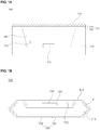
- FIG. 1A and 1B each are cross-sectional views illustrating a light-emitting device package according to one embodiment
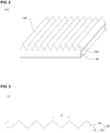
- FIG. 2 is a perspective view illustrating an optical sheet according to one embodiment
- FIG. 3 is a cross-sectional view illustrating an optical sheet according to one embodiment
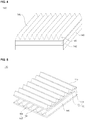
- FIG. 4 is a perspective view illustrating an optical sheet according to one embodiment
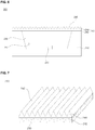
- FIG. 5 is an exploded perspective view illustrating an optical sheet according to one embodiment.
- a light-emitting device package 100 comprises: a body 110 having a cavity 112 formed therein; a light source 130 mounted to the bottom of the body 110; a resin layer 120 which fills the cavity 112 and is transmissive; and an optical sheet 140 provided on the resin layer 120, wherein the optical sheet 140 has a first layer 142, a second layer 144 which is provided on the first layer 142 and includes a plurality of linear prisms 145, wherein the first layer 142 has a first refractive index and the resin layer 120 has a second refractive index, and wherein the first refractive index is equal to or greater than the second refractive index.
- the body 110 may be formed using at least one selected from polyphthalamide (PPA) as a resin material, silicon (Si), aluminum (Al), aluminum nitride (AlN), photosensitive glass (PSG), polyaminde 9T (PA9T), syndiotactic polystyrene (SPS), metal materials, sapphire (Al 2 O 3 ), beryllium oxide (BeO), a printed circuit board (PCB), or the like.
- PPA polyphthalamide
- the body 110 may be formed by injection molding, etching, etc., without being particularly limited thereto.
- the inner surface of the body 110 may be provided with an inclined surface.
- the reflective angle of light emitted from the light source 130 may be varied, depending on the angle of the inclined surface. Accordingly, the orientation angle of light discharged to the outside can be controlled.
- the cavity 112 provided in the body 110 may have various shapes including, but being not limited to, a circular shape, a rectangular shape, a polygonal shape, an oval shape and a shape with curved corners.
- the light source 130 is mounted on bottom of the body 110 and an example of such light source 130 may be an LED.
- the LED may include, without being limited to, color LEDs emitting red, green, blue or white light, or UV LEDs emitting ultraviolet light. Further, at least one LED may be mounted on the body.
- the LED may be a horizontal type LED having electric leads provided on the top of the LED, or a vertical type LED having electric leads provided on the top and bottom of the LED.
- the body 110 may have an electrode (not shown).
- the electrode (not shown) may be electrically connected to the light source 130 to supply power.
- the electrode may comprise at least one selected from titanium (Ti), copper (Cu), nickel (Ni), gold (Au), chromium (Cr), tantalum (Ta), platinum (Pt), tin (Sn), silver (Ag), phosphorous (P), aluminum (Al), indium (In), palladium (Pd), cobalt (Co), silicon (Si), germanium (Ge), hafnium (Hf), ruthenium (Ru), iron (Fe), or alloys thereof.
- the electrode (not shown) may be formed in a single layer or multi-layer structure, without being particularly limited thereto.
- the cavity 112 may include the resin layer 120 having light transmitting property. More particularly, the cavity 112 may be filled with the resin layer 120 having light transmitting property to protect the light source 130 from impurities or moisture.
- the resin layer 120 may be composed of silicone, epoxy or other resin materials and formed by filling the cavity 112 with such a resin material and UV or heat curing the same.
- the light-emitting device package 110 may be a wafer level package, as shown in FIG. 1B .
- a light-emitting device package 100 comprises; a body 110, an electrode layer 150 which is provided on the body and includes a first electrode layer 152 and a second electrode layer 154, a light emitting device 130 provided on the body 110, a resin layer 120 surrounding the light emitting device 130, and an optical sheet 140 placed on the light emitting device 130.
- the body 110 may be made of an electrically insulating material, for example, resin, ceramic, a silicon wafer, etc.
- the body 110 made of a silicon wafer is illustrated in one embodiment.
- a recess may be formed in a concave shape by selectively removing a top surface of the body 110. Within the recess, the light emitting device 130 is located and the resin layer 120 may be formed.
- An insulating layer 114 may be formed on a surface of the body 110.
- the insulating layer 114 may prevent current leakage, to thereby improve electrical stability of the light-emitting device package 100.
- the insulating layer 114 may be formed using a silicon oxide film obtained by oxidation of the body 110, without being particularly limited thereto.
- the first and second electrode layers 152 and 154 may be provided on the insulating layer 114 and electrically isolated from each other.
- the first and second electrode layers 152 and 154 may extend from bottom of the body 110 to the recess formed on top of the body 110.
- the light emitting device 130 may be placed in the recess of the body 110 and electrically connected to the first and second electrode layers 152 and 154, respectively. Although not illustrated, the light emitting devices 130 may be electrically connected to each other via a wire and, preferably, at least one wire.
- the resin layer 120 may be placed in the recess of the body 110 while surrounding the light emitting device 130.
- the resin layer 120 may be a silicone resin or epoxy resin including phosphors.
- the resin layer 120 may have a flat top surface or a curved surface in a convex or concave form.
- the body 110 may be provided with an optical sheet 140 and the optical sheet 140 may have a first layer 142 and a second layer 144 wherein the second layer 144 may have a plurality of linear prisms 145 formed thereon.
- the optical sheet 140 may be made of light transmitting materials and may comprise, without being limited to, at least one selected from polyethylene terephthalate, polycarbonate, polyethylene, polystyrene, polyester resin, polyether resin, epoxy resin, urethane resin, spiroacetyl resin, polybutadiene resin, polythiolpolyene resin, or the like.
- the first layer 142 may be provided as a support to form the second layer 144 thereon.
- the resin layer 120 filling the cavity 112 has a second refractive index while the first layer 142 of the optical sheet 140 has a first refractive index, wherein the first refractive index is equal to or greater than the second refractive index.
- total reflection is a phenomenon in that, if an angle of incidence is greater than a critical angle when light moves from a material having a high refractive index to another material having a relatively lower refractive index, the light is reflected at a boundary between these materials having different refractive indices.
- the refractive index of the resin layer 120 is greater than that of the first layer 142, total reflection may occur at a boundary between the resin layer 120 and the first layer 142. Further, since light may be confined (entrapped) in the cavity 112, light extraction efficiency of the light-emitting device package 100 may be reduced.
- the resin layer 120 has a smaller refractive index than that of the first layer 142 to prevent total reflection at the boundary between the resin layer 120 and the first layer 142, thereby improving luminous efficacy of the light-emitting device package 100.
- the first layer 142 is provided with a second layer 144 including a plurality of linear prisms 145 to refract light.
- the second layer 144 may be formed using acrylic resin, without being particularly limited thereto.
- acrylic resin for example, as described above, at least one selected from polyethylene terephthalate, polycarbonate, polyethylene, polystyrene, polyester resin, polyether resin, epoxy resin, urethane resin, spiroacetyl resin, polybutadiene resin, polythiolpolyene resin, or the like, may be used.
- the second layer 142 may be composed of the same material as the first layer 142 and integrated with the same, without being particularly limited thereto.
- the linear prisms 145 may form a plurality of linear prism patterns which are adjacent to and arranged in parallel to one another along one direction, without being particularly limited thereto.
- a vertical cross-section of the linear prisms may take the shape of a triangle, without being particularly limited thereto.
- a pitch 'D' between two adjacent linear prisms 145 in the second layer 144 may range from 30 to 70 ⁇ m, while a height 'T' of each linear prism may range from 20 to 40 ⁇ m.
- a refractive index of the second layer 145 may range from 1.41 to 1.53 and be equal to or greater than that of the resin layer 130, without being particularly limited thereto.
- the second layer 144 may have a refractive index equal to that of the first layer 142, without being particularly limited thereto.
- the linear prisms 145 may form an isosceles triangle and, in this case, light scattering may be increased.
- the optical sheet 140 having a plurality of linear prisms 145 formed thereon is provided on the light-emitting device package 100, luminance (brightness) and light distribution of the package 100 may be enhanced.
- a third layer 146 may be provided under the first layer 142.
- the third layer 146 may be attached to the bottom of the first layer 142 and, for example, be formed using an acrylic resin having favorable transparency and excellent heat resistance and mechanical properties, thus improving heat resistance of the optical sheet 140.
- acrylic resin may include, for example, polyacrylate or polymethyl methacrylate, without being particularly limited thereto.
- the third layer 146 may comprise at least one selected from polyethylene terephthalate, polycarbonate, polyethylene, polystyrene, polyester resin, polyether resin, epoxy resin, urethane resin, spiroacetyl resin, polybutadiene resin, polythiolpolyene resin, or the like, without being particularly limited thereto.
- the third layer 146 may prevent the optical sheet 140 from being modified by heat generated from the light source 130 and have excellent restoration, thus enabling the optical sheet 140 to return to an original shape thereof at room temperature, even when the optical sheet 140 is modified at high temperature.
- the third layer 146 may protect the optical sheet 140 from being scratched due to external impact or other physical force.
- the optical sheet 140 may include a first optical sheet 160 and a second optical sheet 170.
- the first optical sheet 160 may have a first layer 162 and a second layer 164 or a third layer (not shown) while the second optical sheet 170 may have a first layer 172 and a second layer 174 or a third layer (not shown), without being particularly limited thereto.
- the first optical sheet 160 and second optical sheet 170 may be secured to each other, using an adhesive, without being particularly limited thereto.
- a first linear prism part 165 provided on the second layer 164 of the first optical sheet 160 may extend in a first direction, while a second linear prism part 175 provided on the second layer 174 of the second optical sheet 170 may extend in a second direction forming a first angle relative to the first direction.
- the first angle may be a right angle, without being particularly limited thereto.
- the first and second optical sheets 160 and 170 may upwardly reflect 50% of the light oscillating in a direction, along which the light source 130 is arranged, thereby improving luminous efficacy.
- the first and second linear prism parts 165 and 175 provided on the first and second optical sheets 160 and 170, respectively, may increase refraction, thus improving luminous efficacy.
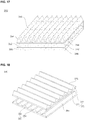
- FIG. 6 is a cross-sectional view illustrating a configuration of a light-emitting device package according to one embodiment
- FIGS. 7 to 11 are perspective views illustrating configurations of optical sheets according to the embodiments
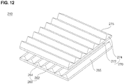
- FIG. 12 is an exploded perspective view illustrating a configuration of an optical sheet according to one embodiment.
- a light-emitting device package 200 comprises: a body 210 having a cavity 212 formed therein; a light source 230 mounted in the cavity 212; a resin layer 220 which fills the cavity 212 and is transmissive; and at least one optical sheet 240 provided on the resin layer 220, wherein each optical sheet 140 has a first layer 242, a second layer 244 which is provided on the first layer 242 and includes a plurality of linear prisms 245, and wherein any one of the first and second layers 242 and 244 includes a phosphor 250.
- the body 210, cavity 212, resin layer 220 and light source 230 are substantially the same as described above and, therefore, a detailed explanation thereof is omitted.
- the first or second layer 242 or 244 may have the phosphor 250.
- the phosphor 250 is uniformly dispersed in a material used for the first or second layer 242 or 244 and then cured, resulting in the first or second layer 242 or 244. Accordingly, the phosphor 250 may be uniformly distributed in the first or second layer 242 or 244.
- Types of the phosphor 250 may be suitably selected, considering the wavelength of light emitted by the light source 230, to allow the light-emitting device package 200 to produce white light.
- the phosphor 250 may be any one selected from a blue light emitting phosphor, blue-green light emitting phosphor, green light emitting phosphor, yellow-green light emitting phosphor, yellow light emitting phosphor, yellow-red light emitting phosphor, orange light emitting phosphor and red light emitting phosphor, depending upon the wavelength of light emitted by the light source 230.
- the phosphor 250 is excited by first light emitted by the light source 230 to create second light.
- the light source 230 is a blue light emitting diode (LED) and the phosphor is a yellow phosphor
- the yellow phosphor is excited by blue light to emit yellow light
- blue light emitted from the blue LED and yellow light excited from the blue light are combined, the light-emitting device package 200 may emit white light.
- the light source 230 is a green LED, a magenta phosphor as well as blue and red phosphors may be employed together.
- a red LED when the light source 230 is a red LED, a cyan phosphor as well as blue and green phosphors may be employed together.
- Such phosphor 250 may be any one commonly known in the art, such as YAG, TAG, sulfide, silicate, aluminate, nitride, carbide, nitride-silicate, borate, fluoride or phosphate based material, etc.
- the phosphor 250 may be distributed in any one of the first layer 242 and the second layer 244 provided with a plurality of linear prisms 245.
- the distribution of the phosphor 250 may be uniform, which in turn improves uniformity and light distribution of the light emitted from the light-emitting device package 200 and protects particles of the phosphor 250 from being degraded by heat generated from the light source 230.
- a third layer 246 may be provided under the first layer 242.
- the third layer 246 may be attached to the bottom of the first layer 242 and, for example, formed using an acrylic resin having favorable transparency and excellent heat resistance and mechanical properties, thus improving heat resistance of the optical sheet 240.
- acrylic resin may include, for example, polyacrylate or polymethyl methacrylate, without being particularly limited thereto.
- the third layer 246 may comprise at least one selected from polyethylene terephthalate, polycarbonate, polyethylene, polystyrene, polyester resin, polyether resin, epoxy resin, urethane resin, spiroacetyl resin, polybutadiene resin, polythiolpolyene resin, or the like, without being particularly limited thereto.
- the third layer 246 may prevent the optical sheet 240 from being modified due to heat generated from the light source 230 and have excellent restoration, thus enabling the optical sheet 240 to return to an original shape thereof at room temperature, even when the optical sheet 240 is modified at a high temperature.
- the third layer 246 may protect the optical sheet 240 from being scratched due to external impact or other physical force.
- the third layer 246 may include the phosphor 250, without being particularly limited thereto.
- the first or second layer 242 or 244 has a first phosphor 252 while the third layer 246 has a second phosphor 254, wherein the first and second phosphors 252 and 254 may be phosphors emitting different wavelengths of light.
- the first phosphor 252 is a red phosphor while the second phosphor 254 is a green phosphor, and these phosphors may be excited by light emitted from the light source 230 to emit white light, without being particularly limited thereto.
- FIG. 12 is an exploded perspective view illustrating a configuration of an optical sheet according to one embodiment.
- the optical sheet 240 may include a first optical sheet 260 and a second optical sheet 270.
- the first optical sheet 260 may have a first layer 262 and a second layer 264, or the second layer 264 may have a third layer (not shown) and a fourth layer (not shown).
- the second optical sheet 270 may have a first layer 272 and a second layer 274, or the second layer 274 may have a third layer (not shown) and a fourth layer (not shown), without being particularly limited thereto.
- at least one of the first and second optical sheets 260 and 270 may include a phosphor, without being particularly limited thereto.
- the first and second optical sheets 260 and 270 may be secured to each other, using an adhesive, without being particularly limited thereto.
- a first linear prism part 265 provided on the second layer 264 of the first optical sheet 260 may extend in a first direction, while a second linear prism part 275 provided on the second layer 274 of the second optical sheet 270 may extend in a second direction forming a first angle relative to the first direction.
- the first angle may be a right angle, without being particularly limited thereto.
- the first and second optical sheets 260 and 270 may upwardly reflect 50% of the light oscillating in a direction, along which the light source 230 is arranged, thereby improving luminous efficacy.
- the first and second linear prism parts 265 and 275 provided on the first and second optical sheets 260 and 270, respectively, may increase refraction, thus improving luminous efficacy.
- FIG. 13 is a cross-sectional view illustrating a configuration of a light-emitting device package according to one embodiment
- FIGS. 14 to 17 are perspective views illustrating configurations of optical sheets according to embodiments
- FIG. 18 is an exploded perspective view illustrating a configuration of an optical sheet according to one embodiment.
- a light-emitting device package 300 comprises: a body 310 having a cavity 312 formed therein; a light source 230 mounted to the bottom of the body 310; a resin layer 320 which fills the cavity 312 and is transmissive; and at least one optical sheet 340 provided on the resin layer 320, wherein each optical sheet 340 has a first layer 342, a second layer 344 which is provided on the first layer 342 and includes a plurality of linear prisms 345, wherein the first layer 342 has a first phosphor 352 while the second layer 344 has a second phosphor 354, and wherein the first and second phosphors 352 and 354 emit different wavelengths of light.
- the body 310, cavity 312, resin layer 320 and light source 330 are substantially the same as described above and, therefore, a detailed explanation thereof is omitted.
- the first layer 342 may have the first phosphor 352 while the second layer 344 has the second phosphor 354, wherein the first and second phosphors 352 and 354 may emit different wavelengths of light.
- the first phosphor 352 is a red phosphor while the second phosphor 354 is a green phosphor, and these phosphors may be excited by light emitted from the light source 330, without being particularly limited thereto.
- the first layer has the first phosphor 352
- the second layer 344 has the second phosphor 354, and these phosphors 352 and 354 emit different wavelengths of light, which in turn enables the light-emitting device package 300 to uniformly emit light and realize white light with high reliability.
- a process of distributing the first and second phosphors 352 and 354 on the optical sheet is described above and a detailed description thereof is omitted.
- a third layer 342 may be provided under the first layer 342.
- the third layer 346 may be attached to the bottom of the first layer 342 and, for example, be formed using an acrylic resin having favorable transparency and excellent heat resistance and mechanical properties, thus improving heat resistance of the optical sheet 340.
- acrylic resin may include, for example, polyacrylate or polymethyl methacrylate, without being particularly limited thereto.
- the third layer 346 may comprise at least one selected from polyethylene terephthalate, polycarbonate, polyethylene, polystyrene, polyester resin, polyether resin, epoxy resin, urethane resin, spiroacetyl resin, polybutadiene resin, polythiolpolyene resin, or the like, without being particularly limited thereto.
- the third layer 346 may prevent the optical sheet 340 from being modified by heat generated from the light source 330 and have excellent restoration, thus enabling the optical sheet 340 to return to an original shape thereof at room temperature, even when the optical sheet 340 is modified at a high temperature.
- the third layer 346 may protect the optical sheet 340 from being scratched due to external impact or other physical force.
- the third layer 346 includes a phosphor. More particularly, according to the invention, the first layer 342 has a first phosphor 352 and the second layer has a second phosphor 354, while the third layer 346 has a third phosphor 356, wherein the first, second and third phosphors 352, 354 and 356 are phosphors emitting different wavelengths of light.
- the first phosphor 352 is a blue phosphor
- the second phosphor 354 is a red phosphor
- the third phosphor 356 is a green phosphor, wherein these phosphors may be excited by light emitted from the light source 330 to emit white light, without being particularly limited thereto.
- FIG. 18 is an exploded perspective view illustrating a configuration of an optical sheet according to one embodiment.
- the optical sheet 340 may include a first optical sheet 360 and a second optical sheet 370.
- the first optical sheet 360 may have a first layer 362 and a second layer 364, or the second layer 364 may have a third layer (not shown) and a fourth layer (not shown).
- the second optical sheet 370 may also have a first layer 372 and a second layer 374, or the second layer 374 may have a third layer (not shown) and a fourth layer (not shown), without being particularly limited thereto.
- at least one of the first and second optical sheets 360 and 370 may include a phosphor, without being particularly limited thereto.
- the first and second optical sheets 360 and 370 may be secured to each other, using an adhesive, without being particularly limited thereto.
- a first linear prism part 365 provided on the second layer 364 of the first optical sheet 360 may extend in a first direction, while a second linear prism part 375 provided on the second layer 374 of the second optical sheet 270 may extend in a second direction forming a first angle relative to the first direction.
- the first angle may be a right angle, without being particularly limited thereto.
- the first and second optical sheets 360 and 370 may upwardly reflect 50% of the light oscillating in a given direction, along which the light source 330 is arranged, thereby improving luminous efficacy.
- the first and second linear prism parts 365 and 375 provided on the first and second optical sheets 360 and 370, respectively, may increase refracted light and thus improve luminous efficacy.
- FIGS. 19 and 20 each schematically illustrate processes of preparing an optical sheet and a light-emitting device package, respectively, according to one embodiment.
- FIGS. 19 and 20 illustrate a process of fabricating a light-emitting device package, e.g., a wafer level package.
- a light-emitting device package e.g., a wafer level package.
- the optical sheet described above may be separately mounted on a single package.
- FIG. 19 illustrates a method for attaching an optical sheet 440 to a silicon wafer 400, wherein the silicon wafer 400 is fabricated by etching a plurality of bodies 410 based on anisotropic etching properties of silicon, placing a light source part in a cavity of each body 410 and filling the cavities with a sealant.
- the optical sheet 440 is adhered to the silicon wafer 400 such that a prism pattern 444 faces upward, wherein the optical sheet 440 may have a first alignment mark 446 while the silicon wafer 400 may have a second alignment mark 402 at a position corresponding to the first alignment mark 446, so as to match alignment between the optical sheet 440 and the silicon wafer 400.
- the optical sheet After coinciding the first alignment mark 446 of the optical sheet 440 with the second alignment mark 402 of the silicon wafer 400, the optical sheet is attached to the silicon wafer 400.
- the method of attaching the optical sheet 440 to the silicon wafer 400 may be selected from, for example: a process that includes coating an adhesive onto a plurality of bodies 410 provided on the silicon wafer 400, adhering the optical sheet 440 thereto and heating the same; a process that includes placing the optical sheet 440 on the silicon wafer 400, and then, applying a predetermined pressure under heating; a process that includes patterning an adhesive on a rear surface of the optical sheet 440 to match with a plurality of bodies 410 provided on the silicon wafer 400, adhering the optical sheet 440 thereto and heating the same, and so forth.
- the silicon wafer 400 After attaching the optical sheet 440 to the silicon wafer 400, the silicon wafer 400 is cut along the plural bodies 410, thus easily fabricating the light-emitting device package described above.
- FIGS. 21 and 22 are cross-sectional views illustrating cross-sections of a light-emitting device package according to one embodiment.
- a light-emitting device 500 includes a step 550 formed on the inner side of a cavity 512, and an optical sheet 540 is fixed to the step 550. Since the body 510, light source 530 and optical sheet 540 are substantially the same as described above, only different features will be described hereinafter.
- the step 550 is provided on at least one region of the inner side of the cavity 512.
- the step 550 may be formed by first forming the cavity 512 on the body 510 and then removing at least one region of the inner side of the cavity 512, without being particularly limited thereto. Further, the step 550 may be formed throughout the inner side of the cavity 512, without being particularly limited thereto.
- the optical sheet 540 is fixed to the step 550.
- the optical sheet 540 may be fixed using an adhesive resin.
- the optical sheet 540 coated with an adhesive resin may be positioned on the step 550 and the optical sheet 540 may be fixed by curing the adhesive resin, without being particularly limited thereto.
- the optical sheet 540 may be reliably secured.
- the cavity 512 is separated into a first cavity 514 and a second cavity 516, according to the invention.
- the first cavity 514 has a first resin layer 520 formed therein while the second cavity 516 includes a second resin layer 522.
- the second resin layer 522 may comprise silicone, epoxy or other resin materials and be formed by filling the cavity 512 with such a resin material, and then, UV or heat curing the same, without being particularly limited thereto.
- the second resin layer 522 may be made of the same material as used for the first resin layer 520, without being particularly limited thereto.
- the optical sheet 540 may be protected from damage caused by external environments.
- the second resin layer 522 includes a second phosphor (not shown).
- the optical sheet 540 has a first phosphor (not shown) while the second resin layer 522 has the second phosphor (not shown), wherein the first and second phosphors (not shown) are different from each other.
- FIG. 23 is a cross-sectional view illustrating a cross-section of a light-emitting device according to one embodiment.
- a light-emitting device package 600 comprise: a body 610 having a cavity 612; a light source 630 mounted to the bottom of the body 610; and an optical sheet 640 provided on the body 610 to cover the cavity 612. Since the body 610, light source 630 and optical sheet 640 are substantially the same as described above, only different features will be described hereinafter.
- the light-emitting device package 610 shown in FIG. 23 further includes, according to the invention, an uneven part 650 formed on the bottom of the body 610 on which the light source 630 is mounted.
- the uneven part 650 may be formed in a uniform shape and a predetermined pattern or, otherwise, have a non-uniform shape.
- the uneven part 650 may allow the light-emitting device package to have a wider visible angle by scattering light emitted by the light source 630, and enable color mixing to be easily conducted, so that colors generated from individual light-emitting device packages 600 may be naturally combined when such light-emitting device packages 600 are connected together to form an array, thereby improving color rendering.
- the uneven part 650 includes, according to the invention, at least one of a concave part or a protrusion part.
- the protrusion part may be protruded above the bottom of the cavity 612 while the concave part may be recessed below the bottom of the cavity 612, without being particularly limited thereto.
- FIG. 24 is a cross-sectional view illustrating a configuration of a light-emitting device package according to one embodiment.
- a light-emitting device package 700 shown in FIG. 24 may have a hole 750 formed on the bottom of a body 710 and the hole 750 may be positioned under a light source 730. Since the body 710, cavity 720 and light source 730 are substantially the same as described above, a detailed description thereof is omitted.
- the light source 730 may be an LED and such an LED may be electrically connected to an electrode (not shown) provided on the body 710.
- the light source 730 and the electrode may be electrically connected together via the hole 750.
- the hole 750 may not only allow the electrical connection described above but also serve as a heat sink to dissipate heat generated from the light source 730 to the outside.
- the hole 750 may be connected to a heat sink plate (not shown) made of metal at the bottom thereof. As such, since the hole 750 is connected to a metal-based heat sink plate having high thermal conductivity, heat dissipation is enhanced.
- FIG. 25 is a perspective view illustrating a lighting instrument equipped with a light-emitting device package according to one embodiment
- FIG. 26 is a cross-sectional view showing a cross section A-A' of the lighting instrument shown in FIG. 25 .
- the lighting instrument 800 is described in terms of a length direction Z, a horizontal direction Y perpendicular to the length direction Z, and a height direction X perpendicular to both the length direction Z and the horizontal direction Y.
- FIG. 26 is a cross-sectional view when viewing in the horizontal direction Y after cutting the lighting instrument 800 along a plane formed of the length direction Z and the height direction X.
- the lighting instrument 800 may include a body 810, a cover 830 coupled with the body 810, and end caps 850 provided to both ends of the body 810.
- the body 810 may be connected with a light-emitting device module 840 at bottom side thereof and, in order to discharge heat generated from a light-emitting device package 844 to the outside through the top of the body 810, the body 810 may be made of metal materials having excellent thermal conductivity and heat dissipation effects.
- the light-emitting device package 844 may be mounted on a PCB 842 with multiple colors and in multiple rows to form an array, and may be spaced from one another by a predetermined interval or, if necessary, by different distances, to control brightness.
- PCB 842 may be a metal core PCB (MPPCB) or PCB made of FR4.
- the light-emitting device package 844 may be coupled with an optical sheet (not shown). If such an optical sheet (not shown) is provided, the light-emitting device package 844 may emit light with enhanced light uniformity and distribution. Moreover, since the optical sheet (not shown) has a linear prism (not shown), collimation of light may be improved, which in turns enhances brightness of the light-emitting device package 844.
- the cover 830 may take the shape of a circle to surround the bottom of the body 810, without being limited thereto.
- the cover 830 protects the light-emitting device module 840 from foreign substances.
- the cover 830 prevents glare occurred by the light-emitting device package 844 and includes diffusion particles to uniformly discharge light to the outside.
- a prism pattern or the like may be formed on at least one of the inner and outer surfaces of the cover 830.
- a phosphor may be applied onto at least one of the inner and outer surfaces of the cover 830.
- the cover 830 should exhibit superior light transmittance to discharge light emitted by the light-emitting device package 844 through the cover 830 to the outside, and the cover 830 should exhibit sufficient heat resistance to endure heat generated from by the light-emitting device package 844.
- the cover 830 is composed of a material including polyethylene terephthalate (PET), polycarbonate (PC) or polymethyl methacrylate (PMMA) and the like.
- the end cap 850 is arranged on both ends of the body 810 and may be used to seal a power device (not shown).
- the end cap 850 is provided with a power pin 852, allowing the lighting instrument 800 to be applied to a terminal from which a conventional fluorescent light has been removed, without using any additional device.
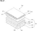
- FIG. 27 is an exploded perspective view illustrating a backlight unit equipped with a light-emitting device package according to one embodiment.
- FIG. 27 illustrates an edge-light type liquid crystal display device 900 which includes a liquid crystal display panel 910 and a backlight unit 970 to supply light to the liquid crystal display panel 910.
- the liquid crystal display panel 910 displays an image using light supplied from the backlight unit 970.
- the liquid crystal display panel 910 includes a color filter substrate 912 and a thin film transistor substrate 914 which face each other through liquid crystal interposed therebetween.
- the color filter substrate 912 can render color images to be displayed through the liquid crystal display panel 910.
- the thin film transistor substrate 914 is electrically connected to a printed circuit board 918 on which a plurality of circuit components is mounted through a driving film 917.
- the thin film transistor substrate 914 responds to drive signals supplied from the printed circuit board 918 and may apply drive voltage from the printed circuit board 418 to liquid crystals.
- the thin film transistor substrate 914 includes a thin film transistor and a pixel electrode formed as a thin film on other substrates composed of a transparent material such as glass or plastic.
- the backlight unit 970 includes; a light-emitting device module 920 to emit light, a light guide plate 930 to convert light emitted by the light-emitting device module 920 into surface light and supply the light to the liquid crystal display panel 910, a plurality of films 950, 766 and 764 to uniformize brightness distribution of light emitted by the light guide plate 930 and improve vertical incidence, and a reflective sheet 940 to reflect light emitted to the back of the light guide plate 930 to the light guide plate 930.
- the light-emitting device module 920 includes a plurality of light-emitting device packages 924 and a PCB 922 on which the light-emitting device packages 924 are mounted to form an array.
- the light-emitting device package 924 may include an optical sheet (not shown) and the optical sheet may improve uniformity and brightness of light emitted by the light-emitting device package 924.
- a backlight unit 970 includes a diffusion film 966 to diffuse light projected from the light guide plate 930 toward the liquid crystal display panel 910, a prism film 950 to concentrate the diffused light and thus improve vertical incidence, and a protective film 964 to protect the prism film 950.
- FIG. 28 is an exploded perspective view illustrating a liquid crystal display including the light emitting device according to one embodiment. However, the contents illustrated and described in FIG. 27 are not mentioned in detail.
- FIG. 28 illustrates a direct-type liquid crystal display device 1000 which includes a liquid crystal display panel 1010 and a backlight unit 1070 to supply light to the liquid crystal display panel 1010.
- the liquid crystal display panel 1010 is substantially the same as described in FIG. 27 and a detailed explanation thereof is omitted.
- the backlight unit 1070 includes a plurality of light-emitting device modules 1023, a reflective sheet 1024, a lower chassis 1030 in which the light-emitting device modules 1023 and the reflective sheet 1024 are accepted, a diffusion plate 1040 arranged on the light-emitting device modules 1023, and a plurality of optical films 1060.
- Each light-emitting device module 1023 includes a plurality of light-emitting device packages 1022 and a PCB 1021 on which the light-emitting device packages 1022 are mounted to form an array.
- the light-emitting device package 1022 may include an optical sheet (not shown) having a phosphor and the optical sheet may improve uniformity and brightness of light emitted by the light-emitting device package 1022.
- the reflective sheet 1024 reflects light emitted from the light-emitting device package 1022 toward the liquid crystal display panel 1010, so as to improve luminous efficacy.
- the optical film 1060 includes a diffusion film 1066, a prism film 1050 and a protective film 1064.
Landscapes
- Engineering & Computer Science (AREA)
- Microelectronics & Electronic Packaging (AREA)
- Physics & Mathematics (AREA)
- Manufacturing & Machinery (AREA)
- Computer Hardware Design (AREA)
- Power Engineering (AREA)
- General Physics & Mathematics (AREA)
- Optics & Photonics (AREA)
- Planar Illumination Modules (AREA)
- Led Device Packages (AREA)
- Non-Portable Lighting Devices Or Systems Thereof (AREA)
Claims (6)
- Composant à dispositif luminescent, comprenant :un corps (510) ayant une cavité (512) formée dans celui-ci ;une diode luminescente (530) montée dans la cavité ;au moins une feuille optique (540) ;une marche (550) formée sur le côté intérieur de la cavité (512), la feuille optique (540) étant fixée à la marche (550) et séparant la cavité (512) en une première partie de cavité (514) et une seconde partie de cavité (516) ; etune première couche de résine (520) qui remplit la première partie de cavité (514) et est transmissive,dans lequel l'au moins une feuille optique (540) est prévue sur la première couche de résine,dans lequel le composant à dispositif luminescent comprend en outre une seconde couche de résine (522) dans la seconde partie de cavité (516) sur la feuille optique (540),caractérisé en ce que la feuille optique comprend une première couche (542), une deuxième couche (544) qui est prévue sur la première couche (542) et comporte une pluralité de prismes linéaires, et une troisième couche (346) formée sous la première couche (542) et agencée entre la première couche et la première couche de résine (520),en ce que la première couche (542) a un premier indice de réfraction et la première couche en résine (520) a un second indice de réfraction,en ce que les première, deuxième et troisième couches (542, 544, 346) de la feuille optique comprennent des luminophores respectifs qui émettent différentes longueurs d'onde de lumière, et la seconde couche de résine (522) comprend un autre luminophore,en ce que le premier indice de réfraction est égal ou supérieur au second indice de réfraction, eten ce qu'une partie irrégulière (650) est formée au fond de la cavité et comprend au moins une partie parmi une partie concave ou une partie saillante.
- Composant à dispositif luminescent selon la revendication 1, dans lequel les plusieurs prismes linéaires forment une pluralité de motifs prismatiques disposés parallèlement les uns aux autres.
- Composant à dispositif luminescent selon la revendication 1 ou 2, dans lequel les prismes linéaires ont un pas allant de 30 à 70 µm.
- Composant à dispositif luminescent selon l'une quelconque des revendications 1 à 3, dans lequel chaque prisme linéaire a une hauteur allant de 20 à 40 µm.
- Composant à dispositif luminescent selon l'une quelconque des revendications 1 à 4, dans lequel la feuille optique comprend une première feuille optique (160) et une seconde feuille optique (170) prévue sur la première feuille optique, dans lequel la première feuille optique a une première partie de prisme (164) agencée dans une première direction tandis que la seconde feuille optique a une seconde partie de prisme (174) agencée en une seconde direction, et dans lequel les première et seconde directions forment un angle.
- Composant à dispositif luminescent selon l'une quelconque des revendications 1 à 5, comprenant en outre un trou (750) formé au fond du corps (710), dans lequel le trou est positionné sous la diode luminescente (730), et dans lequel le trou est raccordé à une plaque dissipatrice de chaleur faite de métal.
Applications Claiming Priority (2)
| Application Number | Priority Date | Filing Date | Title |
|---|---|---|---|
| KR1020100061531A KR20120000975A (ko) | 2010-06-28 | 2010-06-28 | 발광 소자 패키지, 발광 소자 패키지 제조방법, 및 조명 시스템 |
| KR1020100072997A KR20120011252A (ko) | 2010-07-28 | 2010-07-28 | 광학시트 및 이를 포함하는 발광소자패키지 |
Publications (3)
| Publication Number | Publication Date |
|---|---|
| EP2400569A2 EP2400569A2 (fr) | 2011-12-28 |
| EP2400569A3 EP2400569A3 (fr) | 2014-08-13 |
| EP2400569B1 true EP2400569B1 (fr) | 2018-10-24 |
Family
ID=44584774
Family Applications (1)
| Application Number | Title | Priority Date | Filing Date |
|---|---|---|---|
| EP11171506.6A Active EP2400569B1 (fr) | 2010-06-28 | 2011-06-27 | Boîtier de diode électroluminescente |
Country Status (3)
| Country | Link |
|---|---|
| US (1) | US8766526B2 (fr) |
| EP (1) | EP2400569B1 (fr) |
| CN (1) | CN102299239A (fr) |
Families Citing this family (12)
| Publication number | Priority date | Publication date | Assignee | Title |
|---|---|---|---|---|
| CN104969370A (zh) * | 2013-02-04 | 2015-10-07 | 优志旺电机株式会社 | 荧光光源装置 |
| WO2014123145A1 (fr) * | 2013-02-08 | 2014-08-14 | ウシオ電機株式会社 | Dispositif de source de lumière fluorescente |
| CN103579457A (zh) * | 2013-10-23 | 2014-02-12 | 西安重装渭南光电科技有限公司 | 一种led集成封装结构及其方法 |
| CN103712155B (zh) * | 2013-12-24 | 2017-11-03 | 京东方科技集团股份有限公司 | 灯罩、背光模组和显示装置 |
| TW201531772A (zh) * | 2014-02-12 | 2015-08-16 | Lextar Electronics Corp | 背光模組 |
| CN105940506A (zh) * | 2014-02-28 | 2016-09-14 | 松下知识产权经营株式会社 | 发光器件以及发光装置 |
| CN103928591A (zh) * | 2014-04-18 | 2014-07-16 | 深圳市华星光电技术有限公司 | 一种荧光条及使用荧光条的led封装模组 |
| KR102315124B1 (ko) * | 2015-07-02 | 2021-10-20 | 쑤저우 레킨 세미컨덕터 컴퍼니 리미티드 | 발광소자 패키지 |
| CN108303822A (zh) * | 2018-01-23 | 2018-07-20 | 青岛海信电器股份有限公司 | 一种背光模组、显示装置及液晶电视 |
| TWI676067B (zh) * | 2018-05-15 | 2019-11-01 | 友達光電股份有限公司 | 具環境光補償設計的顯示裝置 |
| CN108720799B (zh) * | 2018-06-27 | 2020-10-02 | 芜湖薰衣草知识产权运营有限公司 | 一种医疗用的喉咙照明装置 |
| CN112820803A (zh) * | 2019-11-15 | 2021-05-18 | 深圳市聚飞光学材料有限公司 | 增光膜及其制作方法、发光装置 |
Citations (2)
| Publication number | Priority date | Publication date | Assignee | Title |
|---|---|---|---|---|
| US20070004065A1 (en) * | 2005-06-30 | 2007-01-04 | 3M Innovative Properties Company | Phosphor tape article |
| WO2009014376A2 (fr) * | 2007-07-25 | 2009-01-29 | Lg Innotek Co., Ltd | Dispositif électroluminescent et procédé de fabrication de celui-ci |
Family Cites Families (35)
| Publication number | Priority date | Publication date | Assignee | Title |
|---|---|---|---|---|
| JP4066620B2 (ja) * | 2000-07-21 | 2008-03-26 | 日亜化学工業株式会社 | 発光素子、および発光素子を配置した表示装置ならびに表示装置の製造方法 |
| US20020180909A1 (en) * | 2001-03-26 | 2002-12-05 | Lubart Neil D. | Device having reflective and transmissive properties |
| US6443579B1 (en) * | 2001-05-02 | 2002-09-03 | Kenneth Myers | Field-of-view controlling arrangements |
| JP4822486B2 (ja) * | 2001-09-26 | 2011-11-24 | Nltテクノロジー株式会社 | 半透過反射板及び半透過型液晶表示装置 |
| US6610598B2 (en) * | 2001-11-14 | 2003-08-26 | Solidlite Corporation | Surface-mounted devices of light-emitting diodes with small lens |
| JP2003330111A (ja) * | 2002-05-10 | 2003-11-19 | Olympus Optical Co Ltd | 発光ユニット、照明装置、及び投影表示装置 |
| US6871982B2 (en) * | 2003-01-24 | 2005-03-29 | Digital Optics International Corporation | High-density illumination system |
| US6846089B2 (en) * | 2003-05-16 | 2005-01-25 | 3M Innovative Properties Company | Method for stacking surface structured optical films |
| KR20070010005A (ko) * | 2004-02-18 | 2007-01-19 | 니폰 제온 가부시키가이샤 | 광학 부재, 그의 제조방법 및 디스플레이 장치 |
| US20060083004A1 (en) * | 2004-10-15 | 2006-04-20 | Eastman Kodak Company | Flat-panel area illumination system |
| US20060103777A1 (en) * | 2004-11-15 | 2006-05-18 | 3M Innovative Properties Company | Optical film having a structured surface with rectangular based prisms |
| KR100610278B1 (ko) | 2004-12-14 | 2006-08-09 | 알티전자 주식회사 | 고휘도 백색발광다이오드 및 그의 제조방법 |
| US20060182409A1 (en) * | 2005-02-11 | 2006-08-17 | Eastman Kodak Company | Optical films of differing refractive indices |
| US20060285332A1 (en) * | 2005-06-15 | 2006-12-21 | Goon Wooi K | Compact LED package with reduced field angle |
| US20070001182A1 (en) * | 2005-06-30 | 2007-01-04 | 3M Innovative Properties Company | Structured phosphor tape article |
| KR20070007648A (ko) | 2005-07-11 | 2007-01-16 | 삼성전자주식회사 | 양방향 광전달 반투과 프리즘 시트, 양방향 백라이트어셈블리 및 이를 포함하는 양방향 액정표시장치 |
| JP2007109947A (ja) * | 2005-10-14 | 2007-04-26 | Toyoda Gosei Co Ltd | 蛍光体板及びこれを備えた発光装置 |
| US20070236938A1 (en) * | 2006-03-31 | 2007-10-11 | 3M Innovative Properties Company | Structured Composite Optical Films |
| KR100777410B1 (ko) | 2006-04-13 | 2007-11-19 | 엘지전자 주식회사 | 발광 소자 모듈 및 그 제조 방법 |
| JP5168813B2 (ja) * | 2006-04-14 | 2013-03-27 | ソニー株式会社 | 光学シート、バックライト装置および液晶表示装置 |
| KR20070107261A (ko) * | 2006-05-02 | 2007-11-07 | 삼성전자주식회사 | 광출사모듈 및 이를 갖는 표시장치 |
| WO2008011377A2 (fr) * | 2006-07-17 | 2008-01-24 | 3M Innovative Properties Company | Conditionnement de del avec extracteur convergent |
| CN101122703B (zh) | 2006-08-11 | 2010-12-01 | 鸿富锦精密工业(深圳)有限公司 | 光学板及采用该光学板的背光模组 |
| JP4905009B2 (ja) | 2006-09-12 | 2012-03-28 | 豊田合成株式会社 | 発光装置の製造方法 |
| JPWO2008099834A1 (ja) * | 2007-02-13 | 2010-05-27 | ソニー株式会社 | 光学シートパッケージ体、光学シートユニット、照明装置および表示装置 |
| DE102007043946A1 (de) | 2007-09-14 | 2009-03-19 | Bayerisches Zentrum für Angewandte Energieforschung e.V. | Faserverbünde und deren Verwendung in Vakuumisolationssystemen |
| JP2009128904A (ja) * | 2007-11-26 | 2009-06-11 | Lg Electronics Inc | 光学フィルム及び液晶表示装置 |
| TW200925726A (en) * | 2007-12-14 | 2009-06-16 | Gigno Technology Co Ltd | Light emitting unit and optical film assembly thereof |
| US20090214828A1 (en) * | 2008-02-26 | 2009-08-27 | Vicki Herzl Watkins | Blunt tip prism film and methods for making the same |
| US7825427B2 (en) * | 2008-09-12 | 2010-11-02 | Bridgelux, Inc. | Method and apparatus for generating phosphor film with textured surface |
| US20100123386A1 (en) * | 2008-11-13 | 2010-05-20 | Maven Optronics Corp. | Phosphor-Coated Light Extraction Structures for Phosphor-Converted Light Emitting Devices |
| TWI481069B (zh) | 2008-11-27 | 2015-04-11 | Lextar Electronics Corp | 光學薄膜 |
| KR101255557B1 (ko) | 2008-12-22 | 2013-04-17 | 한국전자통신연구원 | 음절 분리에 기반한 문자열 검색 시스템 및 그 방법 |
| TW201123548A (en) * | 2009-12-25 | 2011-07-01 | Ind Tech Res Inst | A multi-layer stacked LED package |
| KR101754900B1 (ko) * | 2010-04-09 | 2017-07-06 | 엘지이노텍 주식회사 | 발광 소자 |
-
2011
- 2011-06-27 EP EP11171506.6A patent/EP2400569B1/fr active Active
- 2011-06-27 US US13/169,466 patent/US8766526B2/en active Active
- 2011-06-28 CN CN2011101847539A patent/CN102299239A/zh active Pending
Patent Citations (2)
| Publication number | Priority date | Publication date | Assignee | Title |
|---|---|---|---|---|
| US20070004065A1 (en) * | 2005-06-30 | 2007-01-04 | 3M Innovative Properties Company | Phosphor tape article |
| WO2009014376A2 (fr) * | 2007-07-25 | 2009-01-29 | Lg Innotek Co., Ltd | Dispositif électroluminescent et procédé de fabrication de celui-ci |
Also Published As
| Publication number | Publication date |
|---|---|
| EP2400569A2 (fr) | 2011-12-28 |
| EP2400569A3 (fr) | 2014-08-13 |
| US20110316409A1 (en) | 2011-12-29 |
| CN102299239A (zh) | 2011-12-28 |
| US8766526B2 (en) | 2014-07-01 |
Similar Documents
| Publication | Publication Date | Title |
|---|---|---|
| EP2400569B1 (fr) | Boîtier de diode électroluminescente | |
| EP2413389B1 (fr) | Conditionnement de dispositif électroluminescent | |
| KR101659357B1 (ko) | 발광소자패키지 | |
| EP2530754B1 (fr) | Emballage de dispositif électroluminescent et système d'éclairage | |
| US9491856B2 (en) | Light emitting device array and light system | |
| EP2458655B1 (fr) | Boîtier incorporant un dispositif électroluminescent | |
| KR101797968B1 (ko) | 발광소자 패키지 | |
| KR101849126B1 (ko) | 발광소자 패키지 | |
| KR101781047B1 (ko) | 발광 소자 패키지 | |
| KR20130079921A (ko) | 인쇄 회로 기판 | |
| KR101904263B1 (ko) | 발광소자 패키지 | |
| KR101722622B1 (ko) | 발광소자 패키지 | |
| KR20120072737A (ko) | 발광 소자 패키지 | |
| KR20120034484A (ko) | 발광소자 패키지 | |
| KR101883344B1 (ko) | 발광소자 어레이 | |
| KR101894933B1 (ko) | 발광소자 패키지 | |
| KR20130014899A (ko) | 발광소자 패키지 | |
| KR20120011252A (ko) | 광학시트 및 이를 포함하는 발광소자패키지 | |
| KR101722627B1 (ko) | 발광소자 모듈 | |
| KR101735310B1 (ko) | 발광소자 패키지 | |
| KR101843734B1 (ko) | 발광소자 어레이 | |
| KR20120073929A (ko) | 발광소자 패키지 | |
| KR20120035464A (ko) | 발광소자 패키지 | |
| KR20120037264A (ko) | 발광소자 패키지 | |
| KR20120014490A (ko) | 리드 프레임을 포함하는 발광소자 패키지 |
Legal Events
| Date | Code | Title | Description |
|---|---|---|---|
| 17P | Request for examination filed |
Effective date: 20110627 |
|
| AK | Designated contracting states |
Kind code of ref document: A2 Designated state(s): AL AT BE BG CH CY CZ DE DK EE ES FI FR GB GR HR HU IE IS IT LI LT LU LV MC MK MT NL NO PL PT RO RS SE SI SK SM TR |
|
| AX | Request for extension of the european patent |
Extension state: BA ME |
|
| PUAI | Public reference made under article 153(3) epc to a published international application that has entered the european phase |
Free format text: ORIGINAL CODE: 0009012 |
|
| RAP1 | Party data changed (applicant data changed or rights of an application transferred) |
Owner name: LG INNOTEK CO., LTD. |
|
| PUAL | Search report despatched |
Free format text: ORIGINAL CODE: 0009013 |
|
| AK | Designated contracting states |
Kind code of ref document: A3 Designated state(s): AL AT BE BG CH CY CZ DE DK EE ES FI FR GB GR HR HU IE IS IT LI LT LU LV MC MK MT NL NO PL PT RO RS SE SI SK SM TR |
|
| AX | Request for extension of the european patent |
Extension state: BA ME |
|
| RIC1 | Information provided on ipc code assigned before grant |
Ipc: H01L 33/52 20100101ALN20140708BHEP Ipc: F21V 8/00 20060101ALI20140708BHEP Ipc: H01L 33/50 20100101ALN20140708BHEP Ipc: G02B 27/09 20060101ALN20140708BHEP Ipc: H01L 33/58 20100101AFI20140708BHEP |
|
| RBV | Designated contracting states (corrected) |
Designated state(s): AL AT BE BG CH CY CZ DE DK EE ES FI FR GB GR HR HU IE IS IT LI LT LU LV MC MK MT NL NO PL PT RO RS SE SI SK SM TR |
|
| STAA | Information on the status of an ep patent application or granted ep patent |
Free format text: STATUS: EXAMINATION IS IN PROGRESS |
|
| 17Q | First examination report despatched |
Effective date: 20170118 |
|
| RAP1 | Party data changed (applicant data changed or rights of an application transferred) |
Owner name: LG INNOTEK CO., LTD. |
|
| GRAP | Despatch of communication of intention to grant a patent |
Free format text: ORIGINAL CODE: EPIDOSNIGR1 |
|
| STAA | Information on the status of an ep patent application or granted ep patent |
Free format text: STATUS: GRANT OF PATENT IS INTENDED |
|
| RIC1 | Information provided on ipc code assigned before grant |
Ipc: H01L 33/58 20100101AFI20180409BHEP Ipc: H01L 33/50 20100101ALN20180409BHEP Ipc: F21V 8/00 20060101ALI20180409BHEP Ipc: G02B 27/09 20060101ALN20180409BHEP Ipc: H01L 33/52 20100101ALN20180409BHEP |
|
| INTG | Intention to grant announced |
Effective date: 20180430 |
|
| RIC1 | Information provided on ipc code assigned before grant |
Ipc: G02B 6/00 20060101ALI20180417BHEP Ipc: G02B 27/09 20060101ALN20180417BHEP Ipc: H01L 33/50 20100101ALN20180417BHEP Ipc: H01L 33/52 20100101ALN20180417BHEP Ipc: H01L 33/58 20100101AFI20180417BHEP |
|
| GRAS | Grant fee paid |
Free format text: ORIGINAL CODE: EPIDOSNIGR3 |
|
| GRAA | (expected) grant |
Free format text: ORIGINAL CODE: 0009210 |
|
| STAA | Information on the status of an ep patent application or granted ep patent |
Free format text: STATUS: THE PATENT HAS BEEN GRANTED |
|
| AK | Designated contracting states |
Kind code of ref document: B1 Designated state(s): AL AT BE BG CH CY CZ DE DK EE ES FI FR GB GR HR HU IE IS IT LI LT LU LV MC MK MT NL NO PL PT RO RS SE SI SK SM TR |
|
| REG | Reference to a national code |
Ref country code: GB Ref legal event code: FG4D |
|
| REG | Reference to a national code |
Ref country code: CH Ref legal event code: EP |
|
| REG | Reference to a national code |
Ref country code: IE Ref legal event code: FG4D |
|
| REG | Reference to a national code |
Ref country code: AT Ref legal event code: REF Ref document number: 1057715 Country of ref document: AT Kind code of ref document: T Effective date: 20181115 |
|
| REG | Reference to a national code |
Ref country code: DE Ref legal event code: R096 Ref document number: 602011053141 Country of ref document: DE |
|
| REG | Reference to a national code |
Ref country code: NL Ref legal event code: MP Effective date: 20181024 |
|
| REG | Reference to a national code |
Ref country code: LT Ref legal event code: MG4D |
|
| REG | Reference to a national code |
Ref country code: AT Ref legal event code: MK05 Ref document number: 1057715 Country of ref document: AT Kind code of ref document: T Effective date: 20181024 |
|
| PG25 | Lapsed in a contracting state [announced via postgrant information from national office to epo] |
Ref country code: NL Free format text: LAPSE BECAUSE OF FAILURE TO SUBMIT A TRANSLATION OF THE DESCRIPTION OR TO PAY THE FEE WITHIN THE PRESCRIBED TIME-LIMIT Effective date: 20181024 |
|
| PG25 | Lapsed in a contracting state [announced via postgrant information from national office to epo] |
Ref country code: ES Free format text: LAPSE BECAUSE OF FAILURE TO SUBMIT A TRANSLATION OF THE DESCRIPTION OR TO PAY THE FEE WITHIN THE PRESCRIBED TIME-LIMIT Effective date: 20181024 Ref country code: NO Free format text: LAPSE BECAUSE OF FAILURE TO SUBMIT A TRANSLATION OF THE DESCRIPTION OR TO PAY THE FEE WITHIN THE PRESCRIBED TIME-LIMIT Effective date: 20190124 Ref country code: IS Free format text: LAPSE BECAUSE OF FAILURE TO SUBMIT A TRANSLATION OF THE DESCRIPTION OR TO PAY THE FEE WITHIN THE PRESCRIBED TIME-LIMIT Effective date: 20190224 Ref country code: HR Free format text: LAPSE BECAUSE OF FAILURE TO SUBMIT A TRANSLATION OF THE DESCRIPTION OR TO PAY THE FEE WITHIN THE PRESCRIBED TIME-LIMIT Effective date: 20181024 Ref country code: AT Free format text: LAPSE BECAUSE OF FAILURE TO SUBMIT A TRANSLATION OF THE DESCRIPTION OR TO PAY THE FEE WITHIN THE PRESCRIBED TIME-LIMIT Effective date: 20181024 Ref country code: LT Free format text: LAPSE BECAUSE OF FAILURE TO SUBMIT A TRANSLATION OF THE DESCRIPTION OR TO PAY THE FEE WITHIN THE PRESCRIBED TIME-LIMIT Effective date: 20181024 Ref country code: PL Free format text: LAPSE BECAUSE OF FAILURE TO SUBMIT A TRANSLATION OF THE DESCRIPTION OR TO PAY THE FEE WITHIN THE PRESCRIBED TIME-LIMIT Effective date: 20181024 Ref country code: BG Free format text: LAPSE BECAUSE OF FAILURE TO SUBMIT A TRANSLATION OF THE DESCRIPTION OR TO PAY THE FEE WITHIN THE PRESCRIBED TIME-LIMIT Effective date: 20190124 Ref country code: FI Free format text: LAPSE BECAUSE OF FAILURE TO SUBMIT A TRANSLATION OF THE DESCRIPTION OR TO PAY THE FEE WITHIN THE PRESCRIBED TIME-LIMIT Effective date: 20181024 Ref country code: LV Free format text: LAPSE BECAUSE OF FAILURE TO SUBMIT A TRANSLATION OF THE DESCRIPTION OR TO PAY THE FEE WITHIN THE PRESCRIBED TIME-LIMIT Effective date: 20181024 |
|
| PG25 | Lapsed in a contracting state [announced via postgrant information from national office to epo] |
Ref country code: RS Free format text: LAPSE BECAUSE OF FAILURE TO SUBMIT A TRANSLATION OF THE DESCRIPTION OR TO PAY THE FEE WITHIN THE PRESCRIBED TIME-LIMIT Effective date: 20181024 Ref country code: AL Free format text: LAPSE BECAUSE OF FAILURE TO SUBMIT A TRANSLATION OF THE DESCRIPTION OR TO PAY THE FEE WITHIN THE PRESCRIBED TIME-LIMIT Effective date: 20181024 Ref country code: SE Free format text: LAPSE BECAUSE OF FAILURE TO SUBMIT A TRANSLATION OF THE DESCRIPTION OR TO PAY THE FEE WITHIN THE PRESCRIBED TIME-LIMIT Effective date: 20181024 Ref country code: PT Free format text: LAPSE BECAUSE OF FAILURE TO SUBMIT A TRANSLATION OF THE DESCRIPTION OR TO PAY THE FEE WITHIN THE PRESCRIBED TIME-LIMIT Effective date: 20190224 Ref country code: GR Free format text: LAPSE BECAUSE OF FAILURE TO SUBMIT A TRANSLATION OF THE DESCRIPTION OR TO PAY THE FEE WITHIN THE PRESCRIBED TIME-LIMIT Effective date: 20190125 |
|
| REG | Reference to a national code |
Ref country code: DE Ref legal event code: R097 Ref document number: 602011053141 Country of ref document: DE |
|
| PG25 | Lapsed in a contracting state [announced via postgrant information from national office to epo] |
Ref country code: IT Free format text: LAPSE BECAUSE OF FAILURE TO SUBMIT A TRANSLATION OF THE DESCRIPTION OR TO PAY THE FEE WITHIN THE PRESCRIBED TIME-LIMIT Effective date: 20181024 Ref country code: DK Free format text: LAPSE BECAUSE OF FAILURE TO SUBMIT A TRANSLATION OF THE DESCRIPTION OR TO PAY THE FEE WITHIN THE PRESCRIBED TIME-LIMIT Effective date: 20181024 Ref country code: CZ Free format text: LAPSE BECAUSE OF FAILURE TO SUBMIT A TRANSLATION OF THE DESCRIPTION OR TO PAY THE FEE WITHIN THE PRESCRIBED TIME-LIMIT Effective date: 20181024 |
|
| PG25 | Lapsed in a contracting state [announced via postgrant information from national office to epo] |
Ref country code: EE Free format text: LAPSE BECAUSE OF FAILURE TO SUBMIT A TRANSLATION OF THE DESCRIPTION OR TO PAY THE FEE WITHIN THE PRESCRIBED TIME-LIMIT Effective date: 20181024 Ref country code: SM Free format text: LAPSE BECAUSE OF FAILURE TO SUBMIT A TRANSLATION OF THE DESCRIPTION OR TO PAY THE FEE WITHIN THE PRESCRIBED TIME-LIMIT Effective date: 20181024 Ref country code: RO Free format text: LAPSE BECAUSE OF FAILURE TO SUBMIT A TRANSLATION OF THE DESCRIPTION OR TO PAY THE FEE WITHIN THE PRESCRIBED TIME-LIMIT Effective date: 20181024 Ref country code: SK Free format text: LAPSE BECAUSE OF FAILURE TO SUBMIT A TRANSLATION OF THE DESCRIPTION OR TO PAY THE FEE WITHIN THE PRESCRIBED TIME-LIMIT Effective date: 20181024 |
|
| PLBE | No opposition filed within time limit |
Free format text: ORIGINAL CODE: 0009261 |
|
| STAA | Information on the status of an ep patent application or granted ep patent |
Free format text: STATUS: NO OPPOSITION FILED WITHIN TIME LIMIT |
|
| 26N | No opposition filed |
Effective date: 20190725 |
|
| PG25 | Lapsed in a contracting state [announced via postgrant information from national office to epo] |
Ref country code: SI Free format text: LAPSE BECAUSE OF FAILURE TO SUBMIT A TRANSLATION OF THE DESCRIPTION OR TO PAY THE FEE WITHIN THE PRESCRIBED TIME-LIMIT Effective date: 20181024 |
|
| PG25 | Lapsed in a contracting state [announced via postgrant information from national office to epo] |
Ref country code: MC Free format text: LAPSE BECAUSE OF FAILURE TO SUBMIT A TRANSLATION OF THE DESCRIPTION OR TO PAY THE FEE WITHIN THE PRESCRIBED TIME-LIMIT Effective date: 20181024 |
|
| REG | Reference to a national code |
Ref country code: CH Ref legal event code: PL |
|
| GBPC | Gb: european patent ceased through non-payment of renewal fee |
Effective date: 20190627 |
|
| REG | Reference to a national code |
Ref country code: BE Ref legal event code: MM Effective date: 20190630 |
|
| PG25 | Lapsed in a contracting state [announced via postgrant information from national office to epo] |
Ref country code: TR Free format text: LAPSE BECAUSE OF FAILURE TO SUBMIT A TRANSLATION OF THE DESCRIPTION OR TO PAY THE FEE WITHIN THE PRESCRIBED TIME-LIMIT Effective date: 20181024 |
|
| PG25 | Lapsed in a contracting state [announced via postgrant information from national office to epo] |
Ref country code: GB Free format text: LAPSE BECAUSE OF NON-PAYMENT OF DUE FEES Effective date: 20190627 Ref country code: IE Free format text: LAPSE BECAUSE OF NON-PAYMENT OF DUE FEES Effective date: 20190627 |
|
| PG25 | Lapsed in a contracting state [announced via postgrant information from national office to epo] |
Ref country code: LU Free format text: LAPSE BECAUSE OF NON-PAYMENT OF DUE FEES Effective date: 20190627 Ref country code: LI Free format text: LAPSE BECAUSE OF NON-PAYMENT OF DUE FEES Effective date: 20190630 Ref country code: CH Free format text: LAPSE BECAUSE OF NON-PAYMENT OF DUE FEES Effective date: 20190630 Ref country code: BE Free format text: LAPSE BECAUSE OF NON-PAYMENT OF DUE FEES Effective date: 20190630 |
|
| PG25 | Lapsed in a contracting state [announced via postgrant information from national office to epo] |
Ref country code: FR Free format text: LAPSE BECAUSE OF NON-PAYMENT OF DUE FEES Effective date: 20190630 |
|
| PG25 | Lapsed in a contracting state [announced via postgrant information from national office to epo] |
Ref country code: CY Free format text: LAPSE BECAUSE OF FAILURE TO SUBMIT A TRANSLATION OF THE DESCRIPTION OR TO PAY THE FEE WITHIN THE PRESCRIBED TIME-LIMIT Effective date: 20181024 |
|
| PG25 | Lapsed in a contracting state [announced via postgrant information from national office to epo] |
Ref country code: MT Free format text: LAPSE BECAUSE OF FAILURE TO SUBMIT A TRANSLATION OF THE DESCRIPTION OR TO PAY THE FEE WITHIN THE PRESCRIBED TIME-LIMIT Effective date: 20181024 Ref country code: HU Free format text: LAPSE BECAUSE OF FAILURE TO SUBMIT A TRANSLATION OF THE DESCRIPTION OR TO PAY THE FEE WITHIN THE PRESCRIBED TIME-LIMIT; INVALID AB INITIO Effective date: 20110627 |
|
| REG | Reference to a national code |
Ref country code: DE Ref legal event code: R081 Ref document number: 602011053141 Country of ref document: DE Owner name: SUZHOU LEKIN SEMICONDUCTOR CO. LTD., TAICANG, CN Free format text: FORMER OWNER: LG INNOTEK CO., LTD., SEOUL, KR |
|
| PG25 | Lapsed in a contracting state [announced via postgrant information from national office to epo] |
Ref country code: MK Free format text: LAPSE BECAUSE OF FAILURE TO SUBMIT A TRANSLATION OF THE DESCRIPTION OR TO PAY THE FEE WITHIN THE PRESCRIBED TIME-LIMIT Effective date: 20181024 |
|
| PGFP | Annual fee paid to national office [announced via postgrant information from national office to epo] |
Ref country code: DE Payment date: 20230502 Year of fee payment: 13 |