EP2400567A2 - Phosphorauswahl für eine Licht-emittierende Vorrichtung - Google Patents
Phosphorauswahl für eine Licht-emittierende Vorrichtung Download PDFInfo
- Publication number
- EP2400567A2 EP2400567A2 EP11169327A EP11169327A EP2400567A2 EP 2400567 A2 EP2400567 A2 EP 2400567A2 EP 11169327 A EP11169327 A EP 11169327A EP 11169327 A EP11169327 A EP 11169327A EP 2400567 A2 EP2400567 A2 EP 2400567A2
- Authority
- EP
- European Patent Office
- Prior art keywords
- light
- phosphors
- light emitted
- emitting element
- chromaticity coordinates
- Prior art date
- Legal status (The legal status is an assumption and is not a legal conclusion. Google has not performed a legal analysis and makes no representation as to the accuracy of the status listed.)
- Granted
Links
Images

Classifications
-
- H—ELECTRICITY
- H10—SEMICONDUCTOR DEVICES; ELECTRIC SOLID-STATE DEVICES NOT OTHERWISE PROVIDED FOR
- H10H—INORGANIC LIGHT-EMITTING SEMICONDUCTOR DEVICES HAVING POTENTIAL BARRIERS
- H10H20/00—Individual inorganic light-emitting semiconductor devices having potential barriers, e.g. light-emitting diodes [LED]
- H10H20/80—Constructional details
- H10H20/85—Packages
- H10H20/851—Wavelength conversion means
- H10H20/8511—Wavelength conversion means characterised by their material, e.g. binder
- H10H20/8512—Wavelength conversion materials
- H10H20/8513—Wavelength conversion materials having two or more wavelength conversion materials
-
- H—ELECTRICITY
- H01—ELECTRIC ELEMENTS
- H01L—SEMICONDUCTOR DEVICES NOT COVERED BY CLASS H10
- H01L2924/00—Indexing scheme for arrangements or methods for connecting or disconnecting semiconductor or solid-state bodies as covered by H01L24/00
- H01L2924/0001—Technical content checked by a classifier
- H01L2924/0002—Not covered by any one of groups H01L24/00, H01L24/00 and H01L2224/00
-
- H—ELECTRICITY
- H10—SEMICONDUCTOR DEVICES; ELECTRIC SOLID-STATE DEVICES NOT OTHERWISE PROVIDED FOR
- H10H—INORGANIC LIGHT-EMITTING SEMICONDUCTOR DEVICES HAVING POTENTIAL BARRIERS
- H10H20/00—Individual inorganic light-emitting semiconductor devices having potential barriers, e.g. light-emitting diodes [LED]
- H10H20/80—Constructional details
- H10H20/85—Packages
- H10H20/851—Wavelength conversion means
- H10H20/8515—Wavelength conversion means not being in contact with the bodies
Definitions
- the present invention relates to a light-emitting element and a light-emitting device using phosphors that convert a wavelength of light exiting from this light-emitting element.
- a light-emitting diode can emit light with lower power and high luminance, and is used as a light source in various electrical devices such as a display and an illumination fixture.
- LED light-emitting diode
- a blue LED has been put into practice, and the LEDs of these three RGB colors can be combined together or the LED and phosphors converting a wavelength of light exiting from the LED can be combined together to thereby emit light of various colors.
- a light-emitting device which outputs yellow light by providing light of a blue LED to phosphors and mixes blue light and the yellow light to thereby create white light.
- a light-emitting device of this type emitting white light
- YAG-based phosphors are dispersed in a resin material such as silicone resin for sealing the blue LED, and the YAG-based phosphors convert a wavelength of the blue light exiting from the LED to emit the yellow light.
- an isotempearutre line set at 5000K of white color by the blue LED chip and the yellow phosphors and an isotemperature line (with an angle of ⁇ ) with 3500K do not become parallel to each other, thus causing variation in the color temperature.
- a white light-emitting device for example, see Patent literature 1 which controls variation in color temperature by ranking a blue LED to be used in accordance with a wavelength and luminance of emitted light and then adjusting luminance of the light emitted by phosphors so as to correspond to the ranked LED.
- the blue LED and the phosphors are appropriately combined together so that chromaticity coordinates of light emitted by the blue LED and chromaticity coordinates of the light emitted by the phosphors are plotted on an isotemperature line with a predetermined color temperature.
- variation in chromaticity coordinates occurs along on the isotemperature line.
- the isotemperature line is a straight line plotting chromaticity coordinates with the same color temperature on a chromaticity diagram, and variation in chromaticity coordinates along the isotemperature line results in small variation in the color temperature itself.
- an LED light source for example, see Patent literature 2 further provided with a color temperature adjusting member containing phosphors (second phosphors) emitting light of a color different from that of phosphors (first phosphors) emitting yellow light.
- a color temperature adjusting member containing phosphors (second phosphors) emitting light of a color different from that of phosphors (first phosphors) emitting yellow light.
- second phosphors emitting light of a color different from that of phosphors (first phosphors) emitting yellow light.
- the present invention has been made, and it is an object of the present invention to provide a light-emitting device having small variation in color temperature of light mixed by using a light-emitting element such as an LED and phosphors that are excited by light exiting from the light-emitting element to emit light.
- a light-emitting element such as an LED and phosphors that are excited by light exiting from the light-emitting element to emit light.
- a light-emitting device includes: a light-emitting element; first phosphors excited by light emitted by the light-emitting element to emit light; and second phosphors excited by the light emitted by the light-emitting element or the light emitted by the first phosphors to emit light.
- Inclination of a straight line on a chromaticity diagram linking chromaticity coordinates of the light emitted by the first phosphors and chromaticity coordinates of the light emitted by the light-emitting element is adapted to be equal to inclination of an isotemperature line with a predetermined color temperature of light obtained by mixing the light emitted by the light-emitting element, the light emitted by the first phosphors, and the light emitted by the second phosphors.
- chromaticity coordinates of the light emitted by the second phosphors have an x value located on a side higher than the straight line on the chromaticity diagram linking the chromaticity coordinates of the light emitted by the light-emitting element and the chromaticity coordinates of the light emitted by the first phosphors.
- the first phosphors or the second phosphors are adapted to have a combination of a plurality of kinds of phosphor particles to emit light with desired chromaticity coordinates.
- a sealing member of resin sealing the light-emitting element is further provided, and the first phosphors are dispersed in a resin material forming the sealing member.
- a coating member provided in a light take-out direction of the sealing member is further provided, and the second phosphors are dispersed in a resin material or glass forming the coating member.
- a gap is formed between the sealing member and the coating member.
- Variation in color coordinates of light obtained by mixing light emitted by a light-emitting element, light emitted by first phosphors, and light emitted by second phosphors occurs along on an isotemperature line, thus providing the light-emitting device with small variation in color temperature.
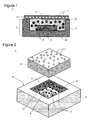
- the light-emitting device 1 of this embodiment is provided with: as shown in Figs. 1 and 2 , a substrate 2 formed with a depressed portion 21; and a light-emitting element 3 mounted at the depressed portion 21 of the substrate 2.
- a sealing member 4 of resin is filled, and to the resin forming this sealing member 4, first phosphors 5 that are excited by light emitted by the light-emitting element 3 to emit light are dispersed.
- a package made by mounting the light-emitting element 3 at the depressed portion 21 of the substrate 2 and filling the sealing member 4 including the first phosphors 5 into the depressed portion 21 is called an LED package 10.
- the LED package 10 has a coating member 6 provided in a light take-out direction of the sealing member 4, and to a resin material or glass forming this coating member 6, second phosphors 7 which are excited by the light emitted by the light-emitting element 3 or the light emitting by the first phosphors 5 to emit light are dispersed.
- the substrate 2 is a substrate for a general-use light-emitting module, and is formed of metal oxide (including ceramic) or metal nitride such as aluminum oxide (Al 2 O 3 ) or aluminum nitride (AIN) having electric insulation properties, or a material such as metal, resin, or glass fiber.
- the depressed portion 21 is formed into a square shape at a substantially central part on a top surface of the substrate 2, and has its bottom surface serving as a mounting surface 22 on which the light-emitting element 3 is mounted. Note that a shape of the depressed portion 21 is not limited to the square shown in the figure and may be of a conic shape or a multi-sided pyramid. Moreover, as long as the mounting surface 22 is coated with an insulation layer, the concave part 21 may be, for example, coated with a metal material having high optical reflectance.
- a wiring patter (not shown) formed of conductive metal such as gold (Au) or silver (Ag), and this wiring pattern is electrically connected to the light-emitting element 3 and an external power terminal part.
- a wiring pattern (not shown) may be provided not on the front surface of the substrate 2 but on a rear surface of the substrate 2. These wiring patterns excluding terminal parts are coated with an insulation layer.
- the light-emitting element 3 is not specifically limited as long as it is a light source that permits emission of light of a desired color as the light-emitting device 1, but a CaN-based blue LED chip that radiates blue light is preferably used.
- a chip of a rectangular plate-like shape is shown as the light-emitting element 3, but a shape of the light-emitting element 3 is not limited to this, and thus the one in accordance with, for example, intended purpose of the light-emitting device 1 is used.
- the light-emitting element 3 has as detailed configuration: a light-emitting part including a laminated structure of a p-type nitride semiconductor layer, a light-emitting layer, and an n-type nitride semiconductor layer; a cathode electrode electrically connected to the n-type nitride semiconductor layer; and an anode electrode electrically connected to the p-type nitride semiconductor layer.
- the cathode electrode and the anode electrode are formed on a bottom surface side of the element, and these cathode electrode and anode electrode are joined to the element terminal part of the wiring pattern via a bump, whereby the light-emitting element 3 is mounted on the substrate 2.
- Illustrated here as a method of mounting the light-emitting element 3 is an example in which a face-down type light-emitting element 3 is mounted with a flip-chip mounted, but the light-emitting element 3 may be a chip of a face-up type, in which case, for example, a method of making connection by use of a dice bond and a wire is used.
- a convex lens member for improving light take-out efficiency may be provided on a light take-out surface of the light-emitting element 3.
- a translucent resin material such as a silicone resin, an epoxy resin, or a modified epoxy resin having properties of these two is used.
- This resin material is kneaded with the first phosphors 5 with predetermined concentration and filled through potting in a manner such as to have a predetermined thickness in the depressed portion 21.
- Used for the first phosphor 5 is a kind in accordance with light-emitting performance such as a color temperature required of the light-emitting device 1 and a light-emitting characteristic including a wavelength of the light emitted by the light-emitting element 3, and kneaded with the resin material in a manner such as to have predetermined concentration.
- a GaN-based blue LED is used as the light-emitting element 3
- preferably used for the first phosphor 5 is a well-known yellow phosphor which is excited by absorbing part of blue light exiting from the light-emitting element 3 and which has a peak wavelength in a wavelength range of 500 to 650 nm.
- This yellow phosphor has a peak wavelength of emitted light in a yellow wavelength range and has a wavelength range of the emitted light including a red wavelength range.
- a so-called YAG-based phosphor including crystals with Garnet composition of complex oxide of Yttrium and Aluminum, although not necessarily limited thereto.
- the first phosphor 5 may be a combination of a plurality of kinds of phosphor particles.
- Used for the coating member 6 is, for example, a member obtained by kneading phosphors with a translucent resin material such as a silicone resin, an epoxy resin, or an acryl resin and forming this phosphor-containing resin material into a sheet-like shape by use of a mold.
- the coating member 6 may be formed by applying the resin material described above onto the light-emitting element 3 through an application method, for example, printing, an inkjet method, or potting.
- a filler or the like may be contained for the purpose of promoting mixed coloring of colors of different light and also improving heat conductivity.
- glass may be used for the coating member 6.
- phosphor-dispersed glass can be produced by mixing together powdery glass and phosphor particles, placing these mixed powders on a framed flat plate, and subjecting them to melt-solidification at reduced-pressure high-temperature atmosphere.
- the second phosphor 7 is, as is the case with the first phosphor 5, the one of a kind in accordance with the light-emitting performance such as the color temperature that is required of the light-emitting device 1 and the light-emitting characteristic such as wavelengths of the light emitted by the light-emitting element 3 and the first phosphor 5 is used, and kneaded with a resin material or a glass material in such a manner as to have predetermined concentration.
- the second phosphors 7 is a well-known orange or red phosphor which is excited by absorbing part of the light emitted by the light-emitting element 3 and the first phosphors 5 and which has a peak wavelength in a wavelength range of 600 to 750 nm.
- SCASN phosphor particles are SCASN phosphor particles.
- the second phosphors 7 may also be a combination of a plurality of kinds of phosphor particles.
- the light emitted by the light-emitting element 3 first excites the first phosphors 5 dispersed in the sealing member 4, and in response to this excitation, the first phosphors 5 emit light.
- the light emitted by the light-emitting element 3 and the light emitted by the first phosphors 5 enter the coating member 6 and excite the second phosphors 7 dispersed in the coating member 6, and in response to this excitation, the first phosphors 5 emit light.
- the light emitted by the light-emitting element 3, the light emitted by the first phosphors 5, and the light emitted by the second phosphors 7 are mixed together in the coating member 6 and exit from a light take-out surface of the coating member 6.
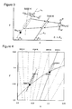
- the light-emitting device 1 mixes together the light emitted by the light-emitting element 3, the emitted by the first phosphors 5, and the light emitted by the second phosphors 7 so that inclination ⁇ 1 of a straight line on a chromaticity diagram linking chromaticity coordinates Y (x Y , y Y ) of the light emitted by the first phosphors 5 and chromaticity coordinates B (x B , y B ) of the light emitted by the light-emitting element 3 becomes equal to inclination ⁇ 2 of an isotemperature line L 2 of light with a predetermined color temperature.
- the predetermined color temperature here is a color temperature desired for the light emitted by the light-emitting device 1 and is 3500K in this embodiment.
- chromaticity coordinates of the light emitted by the second phosphors 7 are R (x R , y R ).
- the chromaticity coordinates of the light emitted by the light-emitting element 3 are measured and its coordinates are plotted on the chromaticity diagram. Then based on the plotted coordinates, a straight line with inclination of an isotemperature line with a color temperature of 3500K is drawn, and a kind, concentration, a mixing ratio, etc. of the first phosphors 5 are determined so that the chromaticity coordinates of the light emitted by the first phosphors 5 are arranged on this straight line.
- Variation in the chromaticity coordinates of the light emitted by the light-emitting element 3 is attributable to manufacturing tolerance of an LED chip, and thus it is difficult to adjust this upon manufacture of the light-emitting device 1.
- the kind, the concentration, the mixing ratio, etc. of the phosphors can be accurately selected and measured and they can be added to the resin material forming the sealing member 4, and thus it is relatively easy to accurately adjust the chromaticity coordinates of the light emitted by the first phosphors 5.
- the adjusted LED package 10 when the light emitted by the first phosphors 5 and the light emitted by the light-emitting element 3 are mixed together, causes variation in chromaticity coordinates of light along the straight line L 1 with the inclination ⁇ 1 the same as the inclination ⁇ 2 of the isotemperature line L 2 with a finally desired color temperature. As a result, the variation in the chromaticity coordinates in the LED package 10 occurs along the straight line L 1 , resulting in large variation in the color temperature.
- the second phosphor 7 as is the case with the first phosphor 5, a kind, concentration, a mixing ratio, etc. of the phosphor can accurately be selected and measured. Moreover, its thickness, form, etc. can be controlled upon machining for formation of the coating member 6, and thus the chromaticity coordinates of the light emitted by the second phosphors 7 can more accurately be adjusted than those of the first phosphors 5.
- variation in the chromaticity coordinates occurs in a manner such as to "shift" towards the chromaticity coordinates R (x R , y R ) of the second phosphors 7 while maintaining the inclination ⁇ 1 of the straight line L 1 , and a range of this variation substantially agree with the isotemperature line L 2 with the color temperature.
- the variation in the chromaticity coordinates of the light emitted by the light-emitting device 1 occurs along on the isotemperature line L 2 , thus resulting in small variation in the color temperature. Consequently, the light-emitting device 1 with small variation in the color temperature can be provided.
- the chromaticity coordinates R of the light emitted by the second phosphors 7 has an x value located on a side higher than the straight line L 1 on the chromaticity diagram linking the chromaticity coordinates B of the light emitted by the light-emitting element 3 and the chromaticity coordinates Y of the light emitted by the first phosphors 5, that is, located on a right side in the chromaticity diagram. That is, the light-emitting element 3 and the first phosphors 5 are combined together to emit light with a high color temperature, and then the second phosphors 7 are combined to shift a color temperature of the mixed light to a low color temperature.
- the color temperature varying along on the straight line L 1 can be shifted to a low color temperature range (right side of the chromaticity diagram) and brought into agreement with the isotemperature line L 2 with a predetermined color temperature, thus reducing the variation in the color temperature.
- the first phosphor 5 may independently emit light with desired chromaticity coordinates Y (x Y , y Y ), or as shown in the figure, a plurality of kinds (two in this example) of phosphors emitting light with different chromaticity coordinates (for example, Y', Y") may be combined together to make adjustment so that light with desired chromaticity coordinates Y (x Y , y Y ) is emitted.
- the second phosphors 7 may also independently emit light with desired chromaticity coordinates R (x R , YR '), or a plurality of kinds (two in this example) of phosphors emitting light with different chromaticity coordinates (for example, R', R) may be combined together.
- the second phosphors 7 in this embodiment shift the variation in the chromaticity coordinates of the light emitted by the LED package 10 to the isotemperature line L 2 of the light with the final color temperature.
- third phosphors (not shown) for including a process of shifting to another chromaticity coordinates during this shift may be included in either of the LED package 10 and the coating member 6.
- a color temperature required of the light exiting from the light-emitting device 1 is 3500K.
- Used for the light-emitting element 3 is a blue LED of a square shape one-mm in diameter and approximately 100 ⁇ m in thickness, as a GaN-based semiconductor emitting blue light with a peak wavelength of approximately 450 nm.
- Used for the substrate 2 is a package substrate of aluminum ceramic having a wiring pattern plated with gold (Au).
- the LED package 10 formed in this manner has a color temperature range of approximately 4800 to 5200K and variation in chromaticity coordinates occurring along on a straight line with the same inclination as that of the isotemperature line with a color temperature of 3500K.
- This variation is mainly attributable to an amount of first phosphors 5 contained, variation in the dispersion of the first phosphors 5, variation in the amount of silicone resin potted, etc.
- the coating member 6 is formed by molding as the second phosphors 7 a sheet-like member which is formed of silicone resin containing 3 wt% of SCASN phosphor particles and which has a thickness of 0.4 mm.
- This coating member 6 is machined by using a mold and thereby its thickness accuracy can be adjusted in units of several ⁇ m, and also the phosphors and the resin can be mixed together and shorten time from when they are injected into the mold to when thermal-curing ends. This results in small variation in dispersion and thickness of the phosphors, which permits small variation in color temperature attributable to the second phosphors 7 included in the coating member 6. As a result, accurate "shift" can be achieved in a manner such that the variation in chromaticity coordinates occurs along on a desired isotemperature line.
- the light-emitting device 1 is manufactured by combining the coating member 6 formed in this manner with the LED package 10.
- the variation in chromaticity coordinates of the light emitted by this light-emitting device 1 occurs along on the isotemperature line with a color temperature of 3500K, with little color temperature variation. This provides the light-emitting device 1 with small color temperature variation.
- Adaptation may be made such that, upon setting the kind, concentration, etc. of the second phosphors 7, the variation in the chromaticity coordinates of the LED package 10 can be "shifted" towards a long wavelength side along a black locus. This provides the light-emitting device 1 capable of emitting light of a natural color.
- the light-emitting device 1 according to this modified example has a gap 8 formed between a sealing member 4 and a coating member 6.
- Other aspects of configuration are the same as that of the embodiment described above.
- the coating member 6, of light emitted by the second phosphors 7, part of the light directed towards an LED package 10 is totally reflected on an interface between the coating member 6 and the gap 8.
- the light exits from a light take-out surface of the coating member 6 with high possibility, resulting in improved light usage efficiency.
- the totally reflected light is further mixed in the coating member 6, thus homogenizing color temperature of the light exiting from the light take-out surface of the coating member 6.
- a filling material or the like for improving light take-out efficiency and heat radiation may be arranged.
- the present invention is not limited to the embodiment described above, and thus various modification can be made to the present invention as long as the inclination ⁇ 1 of the straight line L 1 on the chromaticity diagram linking the chromaticity coordinates Y of the light emitted by the first phosphors 5 and the chromaticity coordinates B of the light emitted by the light-emitting element 3 becomes equal to the inclination ⁇ 2 of the isotemperature line L 2 of light with a desired color temperature.
- the coating member 6 may be a member including a plurality of resin layers having different phosphors dispersed therein, which are combined together to function in the same manner as the second phosphors 7 of this embodiment.
- a light converting member (not shown), for example, which contains fourth phosphors, for further converting a wavelength of light emitted by the light-emitting device 1 may be further provided.
Landscapes
- Led Device Packages (AREA)
- Led Devices (AREA)
- Electroluminescent Light Sources (AREA)
Applications Claiming Priority (1)
| Application Number | Priority Date | Filing Date | Title |
|---|---|---|---|
| JP2010144504A JP5437177B2 (ja) | 2010-06-25 | 2010-06-25 | 発光装置 |
Publications (3)
| Publication Number | Publication Date |
|---|---|
| EP2400567A2 true EP2400567A2 (de) | 2011-12-28 |
| EP2400567A3 EP2400567A3 (de) | 2016-06-22 |
| EP2400567B1 EP2400567B1 (de) | 2017-03-08 |
Family
ID=44654837
Family Applications (1)
| Application Number | Title | Priority Date | Filing Date |
|---|---|---|---|
| EP11169327.1A Not-in-force EP2400567B1 (de) | 2010-06-25 | 2011-06-09 | Phosphorauswahl für eine Licht-emittierende Vorrichtung |
Country Status (4)
| Country | Link |
|---|---|
| US (1) | US8598608B2 (de) |
| EP (1) | EP2400567B1 (de) |
| JP (1) | JP5437177B2 (de) |
| CN (1) | CN102299246B (de) |
Families Citing this family (25)
| Publication number | Priority date | Publication date | Assignee | Title |
|---|---|---|---|---|
| EP2645822A1 (de) * | 2012-03-29 | 2013-10-02 | Koninklijke Philips N.V. | Beleuchtungsvorrichtungen mit mindestens zwei organischen lumineszierenden Materialien |
| JP2014093419A (ja) * | 2012-11-02 | 2014-05-19 | Panasonic Corp | 発光装置の製造方法、発光装置 |
| US8916896B2 (en) * | 2013-02-22 | 2014-12-23 | Cree, Inc. | Light emitter components and methods having improved performance |
| DE102013102482A1 (de) * | 2013-03-12 | 2014-10-02 | Osram Opto Semiconductors Gmbh | Optoelektronisches Bauelement und Verfahren zur Herstellung eines optoelektronischen Bauelements |
| EP2803715B1 (de) * | 2013-05-16 | 2020-02-26 | LG Innotek Co., Ltd. | Phosphor und lichtemittierendes Vorrichtungsgehäuse damit |
| CN111509112B (zh) | 2013-07-08 | 2024-04-02 | 亮锐控股有限公司 | 波长转换的半导体发光器件 |
| TWI580079B (zh) * | 2013-12-26 | 2017-04-21 | 新世紀光電股份有限公司 | 發光二極體封裝結構及發光二極體模組 |
| CN105098025A (zh) | 2014-05-07 | 2015-11-25 | 新世纪光电股份有限公司 | 发光装置 |
| TWI641285B (zh) | 2014-07-14 | 2018-11-11 | 新世紀光電股份有限公司 | 發光模組與發光單元的製作方法 |
| CN104300045B (zh) * | 2014-10-20 | 2017-03-29 | 鸿利智汇集团股份有限公司 | 一种基于多个白光光源混出日光的方法 |
| JP6755090B2 (ja) * | 2014-12-11 | 2020-09-16 | シチズン電子株式会社 | 発光装置及び発光装置の製造方法 |
| US10918747B2 (en) | 2015-07-30 | 2021-02-16 | Vital Vio, Inc. | Disinfecting lighting device |
| WO2017019933A1 (en) | 2015-07-30 | 2017-02-02 | Vital Vio, Inc. | Single diode disinfection |
| TWI622187B (zh) * | 2015-11-23 | 2018-04-21 | 東貝光電科技股份有限公司 | LED light emitting device manufacturing method and LED light emitting device |
| DE102015120775B4 (de) * | 2015-11-30 | 2025-04-30 | OSRAM Opto Semiconductors Gesellschaft mit beschränkter Haftung | Optoelektronisches Bauelement und Hintergrundbeleuchtung für ein Display |
| US20180185533A1 (en) | 2016-12-29 | 2018-07-05 | Vital Vio, Inc. | Control systems for disinfecting light systems and methods of regulating operations of disinfecting light systems |
| JP6964231B2 (ja) * | 2017-04-14 | 2021-11-10 | パナソニックIpマネジメント株式会社 | 波長変換デバイス、光源装置、照明装置、及び、投写型映像表示装置 |
| US10835627B2 (en) | 2017-12-01 | 2020-11-17 | Vital Vio, Inc. | Devices using flexible light emitting layer for creating disinfecting illuminated surface, and related method |
| US10413626B1 (en) * | 2018-03-29 | 2019-09-17 | Vital Vio, Inc. | Multiple light emitter for inactivating microorganisms |
| JP7372512B2 (ja) * | 2018-09-28 | 2023-11-01 | 日亜化学工業株式会社 | 発光装置および発光装置の製造方法 |
| US12194168B2 (en) | 2018-12-19 | 2025-01-14 | Vyv, Inc. | Lighting and dissipation device |
| US11639897B2 (en) | 2019-03-29 | 2023-05-02 | Vyv, Inc. | Contamination load sensing device |
| US11541135B2 (en) | 2019-06-28 | 2023-01-03 | Vyv, Inc. | Multiple band visible light disinfection |
| US11369704B2 (en) | 2019-08-15 | 2022-06-28 | Vyv, Inc. | Devices configured to disinfect interiors |
| US11878084B2 (en) | 2019-09-20 | 2024-01-23 | Vyv, Inc. | Disinfecting light emitting subcomponent |
Citations (2)
| Publication number | Priority date | Publication date | Assignee | Title |
|---|---|---|---|---|
| JP4201167B2 (ja) | 2002-09-26 | 2008-12-24 | シチズン電子株式会社 | 白色発光装置の製造方法 |
| JP2009231569A (ja) | 2008-03-24 | 2009-10-08 | Citizen Holdings Co Ltd | Led光源およびその色度調整方法 |
Family Cites Families (12)
| Publication number | Priority date | Publication date | Assignee | Title |
|---|---|---|---|---|
| JP2608344B2 (ja) | 1990-11-30 | 1997-05-07 | ミサワホーム株式会社 | 長尺材の搬送加工用台車 |
| JP5138145B2 (ja) * | 2002-11-12 | 2013-02-06 | 日亜化学工業株式会社 | 蛍光体積層構造及びそれを用いる光源 |
| JP2005011785A (ja) * | 2003-06-18 | 2005-01-13 | Nobuyuki Motokane | 照明装置 |
| US20050211991A1 (en) * | 2004-03-26 | 2005-09-29 | Kyocera Corporation | Light-emitting apparatus and illuminating apparatus |
| JP4229447B2 (ja) * | 2004-03-31 | 2009-02-25 | スタンレー電気株式会社 | 半導体発光装置及び製造方法 |
| JP4546176B2 (ja) * | 2004-07-16 | 2010-09-15 | 京セラ株式会社 | 発光装置 |
| US7858408B2 (en) * | 2004-11-15 | 2010-12-28 | Koninklijke Philips Electronics N.V. | LED with phosphor tile and overmolded phosphor in lens |
| TW200717866A (en) * | 2005-07-29 | 2007-05-01 | Toshiba Kk | Semiconductor light emitting device |
| KR100930171B1 (ko) * | 2006-12-05 | 2009-12-07 | 삼성전기주식회사 | 백색 발광장치 및 이를 이용한 백색 광원 모듈 |
| CN101271939B (zh) * | 2007-03-23 | 2010-12-15 | 光宝科技股份有限公司 | 具有开回路控制的发光装置及其制造方法 |
| JP5452877B2 (ja) * | 2008-03-13 | 2014-03-26 | パナソニック株式会社 | Led照明装置 |
| EP2104149A1 (de) * | 2008-03-19 | 2009-09-23 | Samsung Electro-Mechanics Co., Ltd | Lichtemittierende Vorrichtung von weißem Licht und Weißlichtquellenmodul damit |
-
2010
- 2010-06-25 JP JP2010144504A patent/JP5437177B2/ja active Active
-
2011
- 2011-06-09 EP EP11169327.1A patent/EP2400567B1/de not_active Not-in-force
- 2011-06-22 US US13/067,716 patent/US8598608B2/en not_active Expired - Fee Related
- 2011-06-24 CN CN201110179990.6A patent/CN102299246B/zh active Active
Patent Citations (2)
| Publication number | Priority date | Publication date | Assignee | Title |
|---|---|---|---|---|
| JP4201167B2 (ja) | 2002-09-26 | 2008-12-24 | シチズン電子株式会社 | 白色発光装置の製造方法 |
| JP2009231569A (ja) | 2008-03-24 | 2009-10-08 | Citizen Holdings Co Ltd | Led光源およびその色度調整方法 |
Also Published As
| Publication number | Publication date |
|---|---|
| US20110316025A1 (en) | 2011-12-29 |
| CN102299246A (zh) | 2011-12-28 |
| CN102299246B (zh) | 2014-05-28 |
| EP2400567B1 (de) | 2017-03-08 |
| JP5437177B2 (ja) | 2014-03-12 |
| JP2012009639A (ja) | 2012-01-12 |
| EP2400567A3 (de) | 2016-06-22 |
| US8598608B2 (en) | 2013-12-03 |
Similar Documents
| Publication | Publication Date | Title |
|---|---|---|
| EP2400567B1 (de) | Phosphorauswahl für eine Licht-emittierende Vorrichtung | |
| US11631791B2 (en) | Semiconductor light-emitting device | |
| US7781783B2 (en) | White light LED device | |
| JP4201167B2 (ja) | 白色発光装置の製造方法 | |
| US9666762B2 (en) | Multi-chip light emitter packages and related methods | |
| EP2334147B1 (de) | Beleuchtungsvorrichtung | |
| KR20120133264A (ko) | 발광소자 렌즈, 이를 포함하는 발광소자 모듈 및 이를 이용한 발광소자 모듈의 제조방법 | |
| JP2009065137A (ja) | 発光装置 | |
| US20130015461A1 (en) | Light-emitting Device Capable of Producing White Light And Light Mixing Method For Producing White Light With Same | |
| JP2011159832A (ja) | 半導体発光装置 | |
| JP2002170999A (ja) | 発光装置及びその製造方法 | |
| JP2017120897A (ja) | 発光装置および調色装置 | |
| JP3604298B2 (ja) | 発光ダイオードの形成方法 | |
| CN102779814A (zh) | 可发出白光的发光元件及其混光方法 | |
| KR20140004505U (ko) | 광혼합식 발광 다이오드의 구조 | |
| JP2003224307A5 (de) | ||
| JPH11243232A (ja) | Led表示装置 | |
| US20130092961A1 (en) | Light emitting device module | |
| JP2007116117A (ja) | 発光装置 | |
| CN100359705C (zh) | 白光二极管制造方法 | |
| CN108321149B (zh) | 发光二极管封装件与发光二极管显示器 | |
| JP4418057B2 (ja) | Ledチップ | |
| KR100748707B1 (ko) | 발광 소자의 제조 방법 | |
| TW201505217A (zh) | 發光二極體封裝結構與發光二極體燈泡 | |
| JP2011159769A (ja) | 半導体発光装置 |
Legal Events
| Date | Code | Title | Description |
|---|---|---|---|
| AK | Designated contracting states |
Kind code of ref document: A2 Designated state(s): AL AT BE BG CH CY CZ DE DK EE ES FI FR GB GR HR HU IE IS IT LI LT LU LV MC MK MT NL NO PL PT RO RS SE SI SK SM TR |
|
| AX | Request for extension of the european patent |
Extension state: BA ME |
|
| PUAI | Public reference made under article 153(3) epc to a published international application that has entered the european phase |
Free format text: ORIGINAL CODE: 0009012 |
|
| RAP1 | Party data changed (applicant data changed or rights of an application transferred) |
Owner name: PANASONIC CORPORATION |
|
| RAP1 | Party data changed (applicant data changed or rights of an application transferred) |
Owner name: PANASONIC INTELLECTUAL PROPERTY MANAGEMENT CO., LT |
|
| PUAL | Search report despatched |
Free format text: ORIGINAL CODE: 0009013 |
|
| AK | Designated contracting states |
Kind code of ref document: A3 Designated state(s): AL AT BE BG CH CY CZ DE DK EE ES FI FR GB GR HR HU IE IS IT LI LT LU LV MC MK MT NL NO PL PT RO RS SE SI SK SM TR |
|
| AX | Request for extension of the european patent |
Extension state: BA ME |
|
| RIC1 | Information provided on ipc code assigned before grant |
Ipc: H01L 33/50 20100101AFI20160518BHEP |
|
| 17P | Request for examination filed |
Effective date: 20160705 |
|
| RBV | Designated contracting states (corrected) |
Designated state(s): AL AT BE BG CH CY CZ DE DK EE ES FI FR GB GR HR HU IE IS IT LI LT LU LV MC MK MT NL NO PL PT RO RS SE SI SK SM TR |
|
| GRAP | Despatch of communication of intention to grant a patent |
Free format text: ORIGINAL CODE: EPIDOSNIGR1 |
|
| STAA | Information on the status of an ep patent application or granted ep patent |
Free format text: STATUS: GRANT OF PATENT IS INTENDED |
|
| INTG | Intention to grant announced |
Effective date: 20161118 |
|
| GRAS | Grant fee paid |
Free format text: ORIGINAL CODE: EPIDOSNIGR3 |
|
| GRAA | (expected) grant |
Free format text: ORIGINAL CODE: 0009210 |
|
| STAA | Information on the status of an ep patent application or granted ep patent |
Free format text: STATUS: THE PATENT HAS BEEN GRANTED |
|
| AK | Designated contracting states |
Kind code of ref document: B1 Designated state(s): AL AT BE BG CH CY CZ DE DK EE ES FI FR GB GR HR HU IE IS IT LI LT LU LV MC MK MT NL NO PL PT RO RS SE SI SK SM TR |
|
| REG | Reference to a national code |
Ref country code: GB Ref legal event code: FG4D |
|
| REG | Reference to a national code |
Ref country code: CH Ref legal event code: EP Ref country code: AT Ref legal event code: REF Ref document number: 874251 Country of ref document: AT Kind code of ref document: T Effective date: 20170315 |
|
| REG | Reference to a national code |
Ref country code: IE Ref legal event code: FG4D |
|
| REG | Reference to a national code |
Ref country code: DE Ref legal event code: R096 Ref document number: 602011035636 Country of ref document: DE |
|
| REG | Reference to a national code |
Ref country code: LT Ref legal event code: MG4D |
|
| REG | Reference to a national code |
Ref country code: NL Ref legal event code: MP Effective date: 20170308 |
|
| PG25 | Lapsed in a contracting state [announced via postgrant information from national office to epo] |
Ref country code: GR Free format text: LAPSE BECAUSE OF FAILURE TO SUBMIT A TRANSLATION OF THE DESCRIPTION OR TO PAY THE FEE WITHIN THE PRESCRIBED TIME-LIMIT Effective date: 20170609 Ref country code: NO Free format text: LAPSE BECAUSE OF FAILURE TO SUBMIT A TRANSLATION OF THE DESCRIPTION OR TO PAY THE FEE WITHIN THE PRESCRIBED TIME-LIMIT Effective date: 20170608 Ref country code: HR Free format text: LAPSE BECAUSE OF FAILURE TO SUBMIT A TRANSLATION OF THE DESCRIPTION OR TO PAY THE FEE WITHIN THE PRESCRIBED TIME-LIMIT Effective date: 20170308 Ref country code: FI Free format text: LAPSE BECAUSE OF FAILURE TO SUBMIT A TRANSLATION OF THE DESCRIPTION OR TO PAY THE FEE WITHIN THE PRESCRIBED TIME-LIMIT Effective date: 20170308 Ref country code: LT Free format text: LAPSE BECAUSE OF FAILURE TO SUBMIT A TRANSLATION OF THE DESCRIPTION OR TO PAY THE FEE WITHIN THE PRESCRIBED TIME-LIMIT Effective date: 20170308 |
|
| REG | Reference to a national code |
Ref country code: AT Ref legal event code: MK05 Ref document number: 874251 Country of ref document: AT Kind code of ref document: T Effective date: 20170308 |
|
| PG25 | Lapsed in a contracting state [announced via postgrant information from national office to epo] |
Ref country code: BG Free format text: LAPSE BECAUSE OF FAILURE TO SUBMIT A TRANSLATION OF THE DESCRIPTION OR TO PAY THE FEE WITHIN THE PRESCRIBED TIME-LIMIT Effective date: 20170608 Ref country code: RS Free format text: LAPSE BECAUSE OF FAILURE TO SUBMIT A TRANSLATION OF THE DESCRIPTION OR TO PAY THE FEE WITHIN THE PRESCRIBED TIME-LIMIT Effective date: 20170308 Ref country code: SE Free format text: LAPSE BECAUSE OF FAILURE TO SUBMIT A TRANSLATION OF THE DESCRIPTION OR TO PAY THE FEE WITHIN THE PRESCRIBED TIME-LIMIT Effective date: 20170308 Ref country code: LV Free format text: LAPSE BECAUSE OF FAILURE TO SUBMIT A TRANSLATION OF THE DESCRIPTION OR TO PAY THE FEE WITHIN THE PRESCRIBED TIME-LIMIT Effective date: 20170308 Ref country code: ES Free format text: LAPSE BECAUSE OF FAILURE TO SUBMIT A TRANSLATION OF THE DESCRIPTION OR TO PAY THE FEE WITHIN THE PRESCRIBED TIME-LIMIT Effective date: 20170308 |
|
| PG25 | Lapsed in a contracting state [announced via postgrant information from national office to epo] |
Ref country code: NL Free format text: LAPSE BECAUSE OF FAILURE TO SUBMIT A TRANSLATION OF THE DESCRIPTION OR TO PAY THE FEE WITHIN THE PRESCRIBED TIME-LIMIT Effective date: 20170308 |
|
| PG25 | Lapsed in a contracting state [announced via postgrant information from national office to epo] |
Ref country code: CZ Free format text: LAPSE BECAUSE OF FAILURE TO SUBMIT A TRANSLATION OF THE DESCRIPTION OR TO PAY THE FEE WITHIN THE PRESCRIBED TIME-LIMIT Effective date: 20170308 Ref country code: AT Free format text: LAPSE BECAUSE OF FAILURE TO SUBMIT A TRANSLATION OF THE DESCRIPTION OR TO PAY THE FEE WITHIN THE PRESCRIBED TIME-LIMIT Effective date: 20170308 Ref country code: IT Free format text: LAPSE BECAUSE OF FAILURE TO SUBMIT A TRANSLATION OF THE DESCRIPTION OR TO PAY THE FEE WITHIN THE PRESCRIBED TIME-LIMIT Effective date: 20170308 Ref country code: EE Free format text: LAPSE BECAUSE OF FAILURE TO SUBMIT A TRANSLATION OF THE DESCRIPTION OR TO PAY THE FEE WITHIN THE PRESCRIBED TIME-LIMIT Effective date: 20170308 Ref country code: RO Free format text: LAPSE BECAUSE OF FAILURE TO SUBMIT A TRANSLATION OF THE DESCRIPTION OR TO PAY THE FEE WITHIN THE PRESCRIBED TIME-LIMIT Effective date: 20170308 Ref country code: SK Free format text: LAPSE BECAUSE OF FAILURE TO SUBMIT A TRANSLATION OF THE DESCRIPTION OR TO PAY THE FEE WITHIN THE PRESCRIBED TIME-LIMIT Effective date: 20170308 |
|
| PG25 | Lapsed in a contracting state [announced via postgrant information from national office to epo] |
Ref country code: SM Free format text: LAPSE BECAUSE OF FAILURE TO SUBMIT A TRANSLATION OF THE DESCRIPTION OR TO PAY THE FEE WITHIN THE PRESCRIBED TIME-LIMIT Effective date: 20170308 Ref country code: IS Free format text: LAPSE BECAUSE OF FAILURE TO SUBMIT A TRANSLATION OF THE DESCRIPTION OR TO PAY THE FEE WITHIN THE PRESCRIBED TIME-LIMIT Effective date: 20170708 Ref country code: PL Free format text: LAPSE BECAUSE OF FAILURE TO SUBMIT A TRANSLATION OF THE DESCRIPTION OR TO PAY THE FEE WITHIN THE PRESCRIBED TIME-LIMIT Effective date: 20170308 Ref country code: PT Free format text: LAPSE BECAUSE OF FAILURE TO SUBMIT A TRANSLATION OF THE DESCRIPTION OR TO PAY THE FEE WITHIN THE PRESCRIBED TIME-LIMIT Effective date: 20170710 |
|
| REG | Reference to a national code |
Ref country code: DE Ref legal event code: R097 Ref document number: 602011035636 Country of ref document: DE |
|
| PLBE | No opposition filed within time limit |
Free format text: ORIGINAL CODE: 0009261 |
|
| STAA | Information on the status of an ep patent application or granted ep patent |
Free format text: STATUS: NO OPPOSITION FILED WITHIN TIME LIMIT |
|
| PG25 | Lapsed in a contracting state [announced via postgrant information from national office to epo] |
Ref country code: DK Free format text: LAPSE BECAUSE OF FAILURE TO SUBMIT A TRANSLATION OF THE DESCRIPTION OR TO PAY THE FEE WITHIN THE PRESCRIBED TIME-LIMIT Effective date: 20170308 Ref country code: MC Free format text: LAPSE BECAUSE OF FAILURE TO SUBMIT A TRANSLATION OF THE DESCRIPTION OR TO PAY THE FEE WITHIN THE PRESCRIBED TIME-LIMIT Effective date: 20170308 |
|
| REG | Reference to a national code |
Ref country code: CH Ref legal event code: PL |
|
| 26N | No opposition filed |
Effective date: 20171211 |
|
| GBPC | Gb: european patent ceased through non-payment of renewal fee |
Effective date: 20170609 |
|
| PG25 | Lapsed in a contracting state [announced via postgrant information from national office to epo] |
Ref country code: SI Free format text: LAPSE BECAUSE OF FAILURE TO SUBMIT A TRANSLATION OF THE DESCRIPTION OR TO PAY THE FEE WITHIN THE PRESCRIBED TIME-LIMIT Effective date: 20170308 |
|
| REG | Reference to a national code |
Ref country code: IE Ref legal event code: MM4A |
|
| REG | Reference to a national code |
Ref country code: FR Ref legal event code: ST Effective date: 20180228 |
|
| PG25 | Lapsed in a contracting state [announced via postgrant information from national office to epo] |
Ref country code: IE Free format text: LAPSE BECAUSE OF NON-PAYMENT OF DUE FEES Effective date: 20170609 Ref country code: GB Free format text: LAPSE BECAUSE OF NON-PAYMENT OF DUE FEES Effective date: 20170609 Ref country code: LI Free format text: LAPSE BECAUSE OF NON-PAYMENT OF DUE FEES Effective date: 20170630 Ref country code: CH Free format text: LAPSE BECAUSE OF NON-PAYMENT OF DUE FEES Effective date: 20170630 Ref country code: LU Free format text: LAPSE BECAUSE OF NON-PAYMENT OF DUE FEES Effective date: 20170609 |
|
| PG25 | Lapsed in a contracting state [announced via postgrant information from national office to epo] |
Ref country code: FR Free format text: LAPSE BECAUSE OF NON-PAYMENT OF DUE FEES Effective date: 20170630 |
|
| REG | Reference to a national code |
Ref country code: BE Ref legal event code: MM Effective date: 20170630 |
|
| PG25 | Lapsed in a contracting state [announced via postgrant information from national office to epo] |
Ref country code: BE Free format text: LAPSE BECAUSE OF NON-PAYMENT OF DUE FEES Effective date: 20170630 |
|
| PG25 | Lapsed in a contracting state [announced via postgrant information from national office to epo] |
Ref country code: MT Free format text: LAPSE BECAUSE OF NON-PAYMENT OF DUE FEES Effective date: 20170609 |
|
| PG25 | Lapsed in a contracting state [announced via postgrant information from national office to epo] |
Ref country code: HU Free format text: LAPSE BECAUSE OF FAILURE TO SUBMIT A TRANSLATION OF THE DESCRIPTION OR TO PAY THE FEE WITHIN THE PRESCRIBED TIME-LIMIT; INVALID AB INITIO Effective date: 20110609 |
|
| PG25 | Lapsed in a contracting state [announced via postgrant information from national office to epo] |
Ref country code: CY Free format text: LAPSE BECAUSE OF NON-PAYMENT OF DUE FEES Effective date: 20170308 |
|
| PGFP | Annual fee paid to national office [announced via postgrant information from national office to epo] |
Ref country code: DE Payment date: 20190729 Year of fee payment: 9 |
|
| PG25 | Lapsed in a contracting state [announced via postgrant information from national office to epo] |
Ref country code: MK Free format text: LAPSE BECAUSE OF FAILURE TO SUBMIT A TRANSLATION OF THE DESCRIPTION OR TO PAY THE FEE WITHIN THE PRESCRIBED TIME-LIMIT Effective date: 20170308 |
|
| PG25 | Lapsed in a contracting state [announced via postgrant information from national office to epo] |
Ref country code: TR Free format text: LAPSE BECAUSE OF FAILURE TO SUBMIT A TRANSLATION OF THE DESCRIPTION OR TO PAY THE FEE WITHIN THE PRESCRIBED TIME-LIMIT Effective date: 20170308 |
|
| PG25 | Lapsed in a contracting state [announced via postgrant information from national office to epo] |
Ref country code: AL Free format text: LAPSE BECAUSE OF FAILURE TO SUBMIT A TRANSLATION OF THE DESCRIPTION OR TO PAY THE FEE WITHIN THE PRESCRIBED TIME-LIMIT Effective date: 20170308 |
|
| REG | Reference to a national code |
Ref country code: DE Ref legal event code: R119 Ref document number: 602011035636 Country of ref document: DE |
|
| PG25 | Lapsed in a contracting state [announced via postgrant information from national office to epo] |
Ref country code: DE Free format text: LAPSE BECAUSE OF NON-PAYMENT OF DUE FEES Effective date: 20210101 |