EP2399284B1 - Semiconductor chip with reinforcement layer - Google Patents
Semiconductor chip with reinforcement layer Download PDFInfo
- Publication number
- EP2399284B1 EP2399284B1 EP10704716.9A EP10704716A EP2399284B1 EP 2399284 B1 EP2399284 B1 EP 2399284B1 EP 10704716 A EP10704716 A EP 10704716A EP 2399284 B1 EP2399284 B1 EP 2399284B1
- Authority
- EP
- European Patent Office
- Prior art keywords
- semiconductor chip
- layer
- frame
- central portion
- substrate
- Prior art date
- Legal status (The legal status is an assumption and is not a legal conclusion. Google has not performed a legal analysis and makes no representation as to the accuracy of the status listed.)
- Not-in-force
Links
Images


Classifications
-
- H—ELECTRICITY
- H01—ELECTRIC ELEMENTS
- H01L—SEMICONDUCTOR DEVICES NOT COVERED BY CLASS H10
- H01L21/00—Processes or apparatus adapted for the manufacture or treatment of semiconductor or solid state devices or of parts thereof
- H01L21/02—Manufacture or treatment of semiconductor devices or of parts thereof
- H01L21/04—Manufacture or treatment of semiconductor devices or of parts thereof the devices having potential barriers, e.g. a PN junction, depletion layer or carrier concentration layer
- H01L21/50—Assembly of semiconductor devices using processes or apparatus not provided for in a single one of the groups H01L21/18 - H01L21/326 or H10D48/04 - H10D48/07 e.g. sealing of a cap to a base of a container
- H01L21/56—Encapsulations, e.g. encapsulation layers, coatings
-
- H—ELECTRICITY
- H01—ELECTRIC ELEMENTS
- H01L—SEMICONDUCTOR DEVICES NOT COVERED BY CLASS H10
- H01L23/00—Details of semiconductor or other solid state devices
- H01L23/28—Encapsulations, e.g. encapsulating layers, coatings, e.g. for protection
- H01L23/31—Encapsulations, e.g. encapsulating layers, coatings, e.g. for protection characterised by the arrangement or shape
- H01L23/3107—Encapsulations, e.g. encapsulating layers, coatings, e.g. for protection characterised by the arrangement or shape the device being completely enclosed
- H01L23/3142—Sealing arrangements between parts, e.g. adhesion promotors
-
- H—ELECTRICITY
- H01—ELECTRIC ELEMENTS
- H01L—SEMICONDUCTOR DEVICES NOT COVERED BY CLASS H10
- H01L21/00—Processes or apparatus adapted for the manufacture or treatment of semiconductor or solid state devices or of parts thereof
- H01L21/02—Manufacture or treatment of semiconductor devices or of parts thereof
- H01L21/04—Manufacture or treatment of semiconductor devices or of parts thereof the devices having potential barriers, e.g. a PN junction, depletion layer or carrier concentration layer
- H01L21/50—Assembly of semiconductor devices using processes or apparatus not provided for in a single one of the groups H01L21/18 - H01L21/326 or H10D48/04 - H10D48/07 e.g. sealing of a cap to a base of a container
- H01L21/56—Encapsulations, e.g. encapsulation layers, coatings
- H01L21/563—Encapsulation of active face of flip-chip device, e.g. underfilling or underencapsulation of flip-chip, encapsulation preform on chip or mounting substrate
-
- H—ELECTRICITY
- H01—ELECTRIC ELEMENTS
- H01L—SEMICONDUCTOR DEVICES NOT COVERED BY CLASS H10
- H01L23/00—Details of semiconductor or other solid state devices
- H01L23/28—Encapsulations, e.g. encapsulating layers, coatings, e.g. for protection
- H01L23/31—Encapsulations, e.g. encapsulating layers, coatings, e.g. for protection characterised by the arrangement or shape
- H01L23/3157—Partial encapsulation or coating
- H01L23/3171—Partial encapsulation or coating the coating being directly applied to the semiconductor body, e.g. passivation layer
-
- H—ELECTRICITY
- H01—ELECTRIC ELEMENTS
- H01L—SEMICONDUCTOR DEVICES NOT COVERED BY CLASS H10
- H01L24/00—Arrangements for connecting or disconnecting semiconductor or solid-state bodies; Methods or apparatus related thereto
- H01L24/01—Means for bonding being attached to, or being formed on, the surface to be connected, e.g. chip-to-package, die-attach, "first-level" interconnects; Manufacturing methods related thereto
- H01L24/02—Bonding areas ; Manufacturing methods related thereto
- H01L24/04—Structure, shape, material or disposition of the bonding areas prior to the connecting process
- H01L24/05—Structure, shape, material or disposition of the bonding areas prior to the connecting process of an individual bonding area
-
- H—ELECTRICITY
- H01—ELECTRIC ELEMENTS
- H01L—SEMICONDUCTOR DEVICES NOT COVERED BY CLASS H10
- H01L2224/00—Indexing scheme for arrangements for connecting or disconnecting semiconductor or solid-state bodies and methods related thereto as covered by H01L24/00
- H01L2224/01—Means for bonding being attached to, or being formed on, the surface to be connected, e.g. chip-to-package, die-attach, "first-level" interconnects; Manufacturing methods related thereto
- H01L2224/02—Bonding areas; Manufacturing methods related thereto
- H01L2224/04—Structure, shape, material or disposition of the bonding areas prior to the connecting process
- H01L2224/0401—Bonding areas specifically adapted for bump connectors, e.g. under bump metallisation [UBM]
-
- H—ELECTRICITY
- H01—ELECTRIC ELEMENTS
- H01L—SEMICONDUCTOR DEVICES NOT COVERED BY CLASS H10
- H01L2224/00—Indexing scheme for arrangements for connecting or disconnecting semiconductor or solid-state bodies and methods related thereto as covered by H01L24/00
- H01L2224/01—Means for bonding being attached to, or being formed on, the surface to be connected, e.g. chip-to-package, die-attach, "first-level" interconnects; Manufacturing methods related thereto
- H01L2224/02—Bonding areas; Manufacturing methods related thereto
- H01L2224/04—Structure, shape, material or disposition of the bonding areas prior to the connecting process
- H01L2224/05—Structure, shape, material or disposition of the bonding areas prior to the connecting process of an individual bonding area
- H01L2224/05001—Internal layers
- H01L2224/0502—Disposition
- H01L2224/05022—Disposition the internal layer being at least partially embedded in the surface
-
- H—ELECTRICITY
- H01—ELECTRIC ELEMENTS
- H01L—SEMICONDUCTOR DEVICES NOT COVERED BY CLASS H10
- H01L2224/00—Indexing scheme for arrangements for connecting or disconnecting semiconductor or solid-state bodies and methods related thereto as covered by H01L24/00
- H01L2224/01—Means for bonding being attached to, or being formed on, the surface to be connected, e.g. chip-to-package, die-attach, "first-level" interconnects; Manufacturing methods related thereto
- H01L2224/02—Bonding areas; Manufacturing methods related thereto
- H01L2224/04—Structure, shape, material or disposition of the bonding areas prior to the connecting process
- H01L2224/05—Structure, shape, material or disposition of the bonding areas prior to the connecting process of an individual bonding area
- H01L2224/05001—Internal layers
- H01L2224/05099—Material
- H01L2224/051—Material with a principal constituent of the material being a metal or a metalloid, e.g. boron [B], silicon [Si], germanium [Ge], arsenic [As], antimony [Sb], tellurium [Te] and polonium [Po], and alloys thereof
- H01L2224/05138—Material with a principal constituent of the material being a metal or a metalloid, e.g. boron [B], silicon [Si], germanium [Ge], arsenic [As], antimony [Sb], tellurium [Te] and polonium [Po], and alloys thereof the principal constituent melting at a temperature of greater than or equal to 950°C and less than 1550°C
- H01L2224/05139—Silver [Ag] as principal constituent
-
- H—ELECTRICITY
- H01—ELECTRIC ELEMENTS
- H01L—SEMICONDUCTOR DEVICES NOT COVERED BY CLASS H10
- H01L2224/00—Indexing scheme for arrangements for connecting or disconnecting semiconductor or solid-state bodies and methods related thereto as covered by H01L24/00
- H01L2224/01—Means for bonding being attached to, or being formed on, the surface to be connected, e.g. chip-to-package, die-attach, "first-level" interconnects; Manufacturing methods related thereto
- H01L2224/02—Bonding areas; Manufacturing methods related thereto
- H01L2224/04—Structure, shape, material or disposition of the bonding areas prior to the connecting process
- H01L2224/05—Structure, shape, material or disposition of the bonding areas prior to the connecting process of an individual bonding area
- H01L2224/05001—Internal layers
- H01L2224/05099—Material
- H01L2224/051—Material with a principal constituent of the material being a metal or a metalloid, e.g. boron [B], silicon [Si], germanium [Ge], arsenic [As], antimony [Sb], tellurium [Te] and polonium [Po], and alloys thereof
- H01L2224/05138—Material with a principal constituent of the material being a metal or a metalloid, e.g. boron [B], silicon [Si], germanium [Ge], arsenic [As], antimony [Sb], tellurium [Te] and polonium [Po], and alloys thereof the principal constituent melting at a temperature of greater than or equal to 950°C and less than 1550°C
- H01L2224/05144—Gold [Au] as principal constituent
-
- H—ELECTRICITY
- H01—ELECTRIC ELEMENTS
- H01L—SEMICONDUCTOR DEVICES NOT COVERED BY CLASS H10
- H01L2224/00—Indexing scheme for arrangements for connecting or disconnecting semiconductor or solid-state bodies and methods related thereto as covered by H01L24/00
- H01L2224/01—Means for bonding being attached to, or being formed on, the surface to be connected, e.g. chip-to-package, die-attach, "first-level" interconnects; Manufacturing methods related thereto
- H01L2224/02—Bonding areas; Manufacturing methods related thereto
- H01L2224/04—Structure, shape, material or disposition of the bonding areas prior to the connecting process
- H01L2224/05—Structure, shape, material or disposition of the bonding areas prior to the connecting process of an individual bonding area
- H01L2224/05001—Internal layers
- H01L2224/05099—Material
- H01L2224/051—Material with a principal constituent of the material being a metal or a metalloid, e.g. boron [B], silicon [Si], germanium [Ge], arsenic [As], antimony [Sb], tellurium [Te] and polonium [Po], and alloys thereof
- H01L2224/05138—Material with a principal constituent of the material being a metal or a metalloid, e.g. boron [B], silicon [Si], germanium [Ge], arsenic [As], antimony [Sb], tellurium [Te] and polonium [Po], and alloys thereof the principal constituent melting at a temperature of greater than or equal to 950°C and less than 1550°C
- H01L2224/05147—Copper [Cu] as principal constituent
-
- H—ELECTRICITY
- H01—ELECTRIC ELEMENTS
- H01L—SEMICONDUCTOR DEVICES NOT COVERED BY CLASS H10
- H01L2224/00—Indexing scheme for arrangements for connecting or disconnecting semiconductor or solid-state bodies and methods related thereto as covered by H01L24/00
- H01L2224/01—Means for bonding being attached to, or being formed on, the surface to be connected, e.g. chip-to-package, die-attach, "first-level" interconnects; Manufacturing methods related thereto
- H01L2224/02—Bonding areas; Manufacturing methods related thereto
- H01L2224/04—Structure, shape, material or disposition of the bonding areas prior to the connecting process
- H01L2224/05—Structure, shape, material or disposition of the bonding areas prior to the connecting process of an individual bonding area
- H01L2224/05001—Internal layers
- H01L2224/05099—Material
- H01L2224/051—Material with a principal constituent of the material being a metal or a metalloid, e.g. boron [B], silicon [Si], germanium [Ge], arsenic [As], antimony [Sb], tellurium [Te] and polonium [Po], and alloys thereof
- H01L2224/05163—Material with a principal constituent of the material being a metal or a metalloid, e.g. boron [B], silicon [Si], germanium [Ge], arsenic [As], antimony [Sb], tellurium [Te] and polonium [Po], and alloys thereof the principal constituent melting at a temperature of greater than 1550°C
- H01L2224/05171—Chromium [Cr] as principal constituent
-
- H—ELECTRICITY
- H01—ELECTRIC ELEMENTS
- H01L—SEMICONDUCTOR DEVICES NOT COVERED BY CLASS H10
- H01L2224/00—Indexing scheme for arrangements for connecting or disconnecting semiconductor or solid-state bodies and methods related thereto as covered by H01L24/00
- H01L2224/01—Means for bonding being attached to, or being formed on, the surface to be connected, e.g. chip-to-package, die-attach, "first-level" interconnects; Manufacturing methods related thereto
- H01L2224/02—Bonding areas; Manufacturing methods related thereto
- H01L2224/04—Structure, shape, material or disposition of the bonding areas prior to the connecting process
- H01L2224/05—Structure, shape, material or disposition of the bonding areas prior to the connecting process of an individual bonding area
- H01L2224/0554—External layer
- H01L2224/0556—Disposition
- H01L2224/05571—Disposition the external layer being disposed in a recess of the surface
- H01L2224/05572—Disposition the external layer being disposed in a recess of the surface the external layer extending out of an opening
-
- H—ELECTRICITY
- H01—ELECTRIC ELEMENTS
- H01L—SEMICONDUCTOR DEVICES NOT COVERED BY CLASS H10
- H01L2224/00—Indexing scheme for arrangements for connecting or disconnecting semiconductor or solid-state bodies and methods related thereto as covered by H01L24/00
- H01L2224/01—Means for bonding being attached to, or being formed on, the surface to be connected, e.g. chip-to-package, die-attach, "first-level" interconnects; Manufacturing methods related thereto
- H01L2224/02—Bonding areas; Manufacturing methods related thereto
- H01L2224/04—Structure, shape, material or disposition of the bonding areas prior to the connecting process
- H01L2224/05—Structure, shape, material or disposition of the bonding areas prior to the connecting process of an individual bonding area
- H01L2224/0554—External layer
- H01L2224/05599—Material
- H01L2224/056—Material with a principal constituent of the material being a metal or a metalloid, e.g. boron [B], silicon [Si], germanium [Ge], arsenic [As], antimony [Sb], tellurium [Te] and polonium [Po], and alloys thereof
- H01L2224/05638—Material with a principal constituent of the material being a metal or a metalloid, e.g. boron [B], silicon [Si], germanium [Ge], arsenic [As], antimony [Sb], tellurium [Te] and polonium [Po], and alloys thereof the principal constituent melting at a temperature of greater than or equal to 950°C and less than 1550°C
- H01L2224/05639—Silver [Ag] as principal constituent
-
- H—ELECTRICITY
- H01—ELECTRIC ELEMENTS
- H01L—SEMICONDUCTOR DEVICES NOT COVERED BY CLASS H10
- H01L2224/00—Indexing scheme for arrangements for connecting or disconnecting semiconductor or solid-state bodies and methods related thereto as covered by H01L24/00
- H01L2224/01—Means for bonding being attached to, or being formed on, the surface to be connected, e.g. chip-to-package, die-attach, "first-level" interconnects; Manufacturing methods related thereto
- H01L2224/02—Bonding areas; Manufacturing methods related thereto
- H01L2224/04—Structure, shape, material or disposition of the bonding areas prior to the connecting process
- H01L2224/05—Structure, shape, material or disposition of the bonding areas prior to the connecting process of an individual bonding area
- H01L2224/0554—External layer
- H01L2224/05599—Material
- H01L2224/056—Material with a principal constituent of the material being a metal or a metalloid, e.g. boron [B], silicon [Si], germanium [Ge], arsenic [As], antimony [Sb], tellurium [Te] and polonium [Po], and alloys thereof
- H01L2224/05638—Material with a principal constituent of the material being a metal or a metalloid, e.g. boron [B], silicon [Si], germanium [Ge], arsenic [As], antimony [Sb], tellurium [Te] and polonium [Po], and alloys thereof the principal constituent melting at a temperature of greater than or equal to 950°C and less than 1550°C
- H01L2224/05644—Gold [Au] as principal constituent
-
- H—ELECTRICITY
- H01—ELECTRIC ELEMENTS
- H01L—SEMICONDUCTOR DEVICES NOT COVERED BY CLASS H10
- H01L2224/00—Indexing scheme for arrangements for connecting or disconnecting semiconductor or solid-state bodies and methods related thereto as covered by H01L24/00
- H01L2224/01—Means for bonding being attached to, or being formed on, the surface to be connected, e.g. chip-to-package, die-attach, "first-level" interconnects; Manufacturing methods related thereto
- H01L2224/02—Bonding areas; Manufacturing methods related thereto
- H01L2224/04—Structure, shape, material or disposition of the bonding areas prior to the connecting process
- H01L2224/05—Structure, shape, material or disposition of the bonding areas prior to the connecting process of an individual bonding area
- H01L2224/0554—External layer
- H01L2224/05599—Material
- H01L2224/056—Material with a principal constituent of the material being a metal or a metalloid, e.g. boron [B], silicon [Si], germanium [Ge], arsenic [As], antimony [Sb], tellurium [Te] and polonium [Po], and alloys thereof
- H01L2224/05638—Material with a principal constituent of the material being a metal or a metalloid, e.g. boron [B], silicon [Si], germanium [Ge], arsenic [As], antimony [Sb], tellurium [Te] and polonium [Po], and alloys thereof the principal constituent melting at a temperature of greater than or equal to 950°C and less than 1550°C
- H01L2224/05647—Copper [Cu] as principal constituent
-
- H—ELECTRICITY
- H01—ELECTRIC ELEMENTS
- H01L—SEMICONDUCTOR DEVICES NOT COVERED BY CLASS H10
- H01L2224/00—Indexing scheme for arrangements for connecting or disconnecting semiconductor or solid-state bodies and methods related thereto as covered by H01L24/00
- H01L2224/01—Means for bonding being attached to, or being formed on, the surface to be connected, e.g. chip-to-package, die-attach, "first-level" interconnects; Manufacturing methods related thereto
- H01L2224/02—Bonding areas; Manufacturing methods related thereto
- H01L2224/04—Structure, shape, material or disposition of the bonding areas prior to the connecting process
- H01L2224/05—Structure, shape, material or disposition of the bonding areas prior to the connecting process of an individual bonding area
- H01L2224/0554—External layer
- H01L2224/05599—Material
- H01L2224/056—Material with a principal constituent of the material being a metal or a metalloid, e.g. boron [B], silicon [Si], germanium [Ge], arsenic [As], antimony [Sb], tellurium [Te] and polonium [Po], and alloys thereof
- H01L2224/05638—Material with a principal constituent of the material being a metal or a metalloid, e.g. boron [B], silicon [Si], germanium [Ge], arsenic [As], antimony [Sb], tellurium [Te] and polonium [Po], and alloys thereof the principal constituent melting at a temperature of greater than or equal to 950°C and less than 1550°C
- H01L2224/05655—Nickel [Ni] as principal constituent
-
- H—ELECTRICITY
- H01—ELECTRIC ELEMENTS
- H01L—SEMICONDUCTOR DEVICES NOT COVERED BY CLASS H10
- H01L2224/00—Indexing scheme for arrangements for connecting or disconnecting semiconductor or solid-state bodies and methods related thereto as covered by H01L24/00
- H01L2224/01—Means for bonding being attached to, or being formed on, the surface to be connected, e.g. chip-to-package, die-attach, "first-level" interconnects; Manufacturing methods related thereto
- H01L2224/10—Bump connectors; Manufacturing methods related thereto
- H01L2224/15—Structure, shape, material or disposition of the bump connectors after the connecting process
- H01L2224/16—Structure, shape, material or disposition of the bump connectors after the connecting process of an individual bump connector
- H01L2224/161—Disposition
- H01L2224/16151—Disposition the bump connector connecting between a semiconductor or solid-state body and an item not being a semiconductor or solid-state body, e.g. chip-to-substrate, chip-to-passive
- H01L2224/16221—Disposition the bump connector connecting between a semiconductor or solid-state body and an item not being a semiconductor or solid-state body, e.g. chip-to-substrate, chip-to-passive the body and the item being stacked
- H01L2224/16225—Disposition the bump connector connecting between a semiconductor or solid-state body and an item not being a semiconductor or solid-state body, e.g. chip-to-substrate, chip-to-passive the body and the item being stacked the item being non-metallic, e.g. insulating substrate with or without metallisation
-
- H—ELECTRICITY
- H01—ELECTRIC ELEMENTS
- H01L—SEMICONDUCTOR DEVICES NOT COVERED BY CLASS H10
- H01L2224/00—Indexing scheme for arrangements for connecting or disconnecting semiconductor or solid-state bodies and methods related thereto as covered by H01L24/00
- H01L2224/01—Means for bonding being attached to, or being formed on, the surface to be connected, e.g. chip-to-package, die-attach, "first-level" interconnects; Manufacturing methods related thereto
- H01L2224/26—Layer connectors, e.g. plate connectors, solder or adhesive layers; Manufacturing methods related thereto
- H01L2224/31—Structure, shape, material or disposition of the layer connectors after the connecting process
- H01L2224/32—Structure, shape, material or disposition of the layer connectors after the connecting process of an individual layer connector
- H01L2224/321—Disposition
- H01L2224/32151—Disposition the layer connector connecting between a semiconductor or solid-state body and an item not being a semiconductor or solid-state body, e.g. chip-to-substrate, chip-to-passive
- H01L2224/32221—Disposition the layer connector connecting between a semiconductor or solid-state body and an item not being a semiconductor or solid-state body, e.g. chip-to-substrate, chip-to-passive the body and the item being stacked
- H01L2224/32225—Disposition the layer connector connecting between a semiconductor or solid-state body and an item not being a semiconductor or solid-state body, e.g. chip-to-substrate, chip-to-passive the body and the item being stacked the item being non-metallic, e.g. insulating substrate with or without metallisation
-
- H—ELECTRICITY
- H01—ELECTRIC ELEMENTS
- H01L—SEMICONDUCTOR DEVICES NOT COVERED BY CLASS H10
- H01L2224/00—Indexing scheme for arrangements for connecting or disconnecting semiconductor or solid-state bodies and methods related thereto as covered by H01L24/00
- H01L2224/73—Means for bonding being of different types provided for in two or more of groups H01L2224/10, H01L2224/18, H01L2224/26, H01L2224/34, H01L2224/42, H01L2224/50, H01L2224/63, H01L2224/71
- H01L2224/732—Location after the connecting process
- H01L2224/73201—Location after the connecting process on the same surface
- H01L2224/73203—Bump and layer connectors
- H01L2224/73204—Bump and layer connectors the bump connector being embedded into the layer connector
-
- H—ELECTRICITY
- H01—ELECTRIC ELEMENTS
- H01L—SEMICONDUCTOR DEVICES NOT COVERED BY CLASS H10
- H01L2924/00—Indexing scheme for arrangements or methods for connecting or disconnecting semiconductor or solid-state bodies as covered by H01L24/00
- H01L2924/01—Chemical elements
- H01L2924/01046—Palladium [Pd]
-
- H—ELECTRICITY
- H01—ELECTRIC ELEMENTS
- H01L—SEMICONDUCTOR DEVICES NOT COVERED BY CLASS H10
- H01L2924/00—Indexing scheme for arrangements or methods for connecting or disconnecting semiconductor or solid-state bodies as covered by H01L24/00
- H01L2924/01—Chemical elements
- H01L2924/01078—Platinum [Pt]
-
- H—ELECTRICITY
- H01—ELECTRIC ELEMENTS
- H01L—SEMICONDUCTOR DEVICES NOT COVERED BY CLASS H10
- H01L2924/00—Indexing scheme for arrangements or methods for connecting or disconnecting semiconductor or solid-state bodies as covered by H01L24/00
- H01L2924/01—Chemical elements
- H01L2924/01079—Gold [Au]
-
- H—ELECTRICITY
- H01—ELECTRIC ELEMENTS
- H01L—SEMICONDUCTOR DEVICES NOT COVERED BY CLASS H10
- H01L2924/00—Indexing scheme for arrangements or methods for connecting or disconnecting semiconductor or solid-state bodies as covered by H01L24/00
- H01L2924/013—Alloys
- H01L2924/0132—Binary Alloys
- H01L2924/01322—Eutectic Alloys, i.e. obtained by a liquid transforming into two solid phases
-
- H—ELECTRICITY
- H01—ELECTRIC ELEMENTS
- H01L—SEMICONDUCTOR DEVICES NOT COVERED BY CLASS H10
- H01L2924/00—Indexing scheme for arrangements or methods for connecting or disconnecting semiconductor or solid-state bodies as covered by H01L24/00
- H01L2924/10—Details of semiconductor or other solid state devices to be connected
- H01L2924/11—Device type
- H01L2924/12—Passive devices, e.g. 2 terminal devices
- H01L2924/1204—Optical Diode
- H01L2924/12044—OLED
-
- H—ELECTRICITY
- H01—ELECTRIC ELEMENTS
- H01L—SEMICONDUCTOR DEVICES NOT COVERED BY CLASS H10
- H01L2924/00—Indexing scheme for arrangements or methods for connecting or disconnecting semiconductor or solid-state bodies as covered by H01L24/00
- H01L2924/19—Details of hybrid assemblies other than the semiconductor or other solid state devices to be connected
- H01L2924/1901—Structure
- H01L2924/1904—Component type
- H01L2924/19041—Component type being a capacitor
Definitions
- This invention relates generally to semiconductor processing, and more particularly to semiconductor chip crack stops and to methods of making the same.
- Dicing saws are made with great care and operate more precisely than a comparable masonry circular saw. Despite these refinements, the dicing saw still imposes significant stresses on the individual dice as they are cut. These stresses and impact loads during the cutting operation can cause microscopic fractures in the dice, particularly at the die corners.
- the cracks introduced during cutting may propagate further into the center of the dice due to thermal stresses and other mechanical stresses that may be placed on the die.
- new cracks may form, particularly near the corners which create so-called stress risers by virtue of their geometries.
- a conventional technique for addressing the propagation of cracks from the corners of a die involves the use of a crack stop.
- a conventional crack stop consists of a frame-like structure formed in and near the edges of the semiconductor die. When viewed from above, the crack stop looks like a picture frame. The conventional crack stop does not extend out to the edges of the conventional die. Because of this geometry, a crack propagating from the corner of a die can achieve a significant length before encountering the die crack stop. If the crack achieves a certain critical length before encountering the conventional crack stop, the crack can become virtually uncontrollable. The crack can overwhelm the conventional crack stop and invade the active portion of the semiconductor die and lay waste to the delicate circuit structures positioned therein.
- Another source of potentially damage-causing cracks is a weakness at the interface between an under bump polyimide layer and an underfill material layer.
- an array of solder joints electrically connects the chip to the underlying substrate.
- the mounting establishes an interface region bounded vertically on one side by the package substrate and on the other by a polyimide layer.
- the conventional polyimide layer is a continuous sheet that blankets the front side of the semiconductor chip.
- a neutral point usually though not necessarily located at the center of the chip, represents an area of substantially zero thermal strain. Solder joints in or near this area suffer low strains.
- the die and underlying substrate begin to exhibit thermal strains that depend on temperature, coefficient of thermal expansion (CTE) and distance from the neutral point.
- CTE coefficient of thermal expansion
- a substrate usually has CTE that is six to seven times larger than the CTE of the chip.
- an underfill material is deposited between the polyimide layer of the semiconductor chip and the package substrate and hardened by a curing process.
- Crack propagation initiates at or in the proximity of the polyimide-to-underfill interface and grows. As a crack grows in length its driving forces increase. Once a crack has gained a critical driving force or so-called “critical energy release rate" the crack will gain enough energy to penetrate through the active bumps and permanently damage the packaged device.
- a conventional technique to compensate for polyimide-to-underfill interface cracks involves a roughening of the polyimide sheet surface.
- the increase in interface strength is directly proportional to the increase in interface area.
- the increase in area may be quite small.
- the present invention is directed to overcoming or reducing the effects of one or more of the foregoing disadvantages.
- a semiconductor chip with a crack resistant polymer layer includes a semiconductor chip with a side on which a polymer layer is applied.
- the polymer layer has a central portion and a first frame portion spatially separated from the central portion to define a first channel.
- underfill material fills into the channel to create a crack resistant interface. Additional details will now be described.
- FIG. 1 is a partially exploded pictorial view of a semiconductor chip package 10 that includes a semiconductor chip 15 mounted on a package substrate 20.
- the package 10 may be provided with a lid 25 that is shown exploded from the package substrate 20.
- a small portion of an underfill material layer 30 is visible at the periphery of the semiconductor chip 15.
- FIG. 2 is an overhead view of the package 10 without the optional lid 25.
- the backside 35 of the semiconductor chip 15 is visible in both FIGS. 1 and 2 .
- the semiconductor chip 15 may be flip-chip mounted to the substrate 20 as shown and electrically connected to conductors in the substrate 20 by interconnects that are not visible in FIG. 1 but will be shown in subsequent figures.
- the semiconductor chip 15 may be any of a myriad of different types of circuit devices used in electronics, such as, for example, microprocessors, graphics processors, combined microprocessor/graphics processors, application specific integrated circuits, memory devices or the like, and may be single or multi-core.
- the semiconductor chip 15 may be fabricated using silicon, germanium or other semiconductor materials. If desired, the chip 15 may be fabricated as a semiconductor-on-insulator substrate or as bulk semiconductor.
- the semiconductor chip 15 may be electrically interconnected with the substrate 20 by a plurality of conductor structures that are not visible in FIG. 1 .
- the substrate 20 may be composed of ceramics or organic materials as desired. If organic, the substrate 20 may actually consist of multiple layers of metallization and dielectric materials that electrically interconnect the semiconductor chip 15 to some other component, such as a board (not shown). The substrate 20 may interconnect electrically with external devices, such as another circuit board, in a variety of ways, such as via a pin grid array, a land grid array, a ball grid array or other configuration.
- the number of individual layers for the substrate 20 is largely a matter of design discretion. In certain exemplary embodiments, the number of layers may vary from four to sixteen. If such a build-up design is selected, a standard core, thin core or coreless arrangement may be used.
- the dielectric materials may be, for example, epoxy resin with or without fiberglass fill.
- the substrate 20 could be configured as something other than a package substrate, such as a printed circuit board serving as a motherboard, a daughter board, a card or some other type of board.
- the underfill material 30 is designed to lessen the effects of differences in CTE between the chip 15 and the substrate 20.
- the underfill material 30 may be composed of well-known epoxy materials, such as epoxy resin with or without silica fillers and phenol resins or the like. Two examples are types 8437-2 and 2BD available from Namics.
- the optional lid 25 may be configured as a top hat design as disclosed, as a bathtub design or some other configuration.
- the lid 25 may be composed of well-known plastics, ceramics or metallic materials as desired. Some exemplary materials include nickel plated copper, anodized aluminum, aluminum-silicon-carbon, aluminum nitride, boron nitride or the like.
- the lid 25 may be secured to the substrate 20 by an adhesive composed of a well-known thixotropic adhesive or other well-known type of package adhesive as desired. However, the lid 25 may be omitted entirely if a lidless design is desired.
- FIG. 3 is a pictorial view of the semiconductor chip 15 flipped over to reveal a front side 40. In this view, the backside 35 of the semiconductor chip 15 is obscured.
- the semiconductor chip 15 may include a bulk semiconductor portion 45, an active circuitry layer 47 positioned on the bulk semiconductor layer 45 and an interconnect layer 50 positioned on the active circuitry layer 47. If the chip 15 is implemented as a semiconductor on insulator design, then a buried insulating layer may be positioned either within the active circuitry layer 47 or in between the circuitry layer 47 and the underlying bulk semiconductor layer 45.
- the active circuitry layer 47 includes the multitudes of transistors, capacitors, resistors and other circuit devices that perform various functions.
- the interconnect layer 50 may consist of plural stacked conductor and interlevel dielectric layers.
- a thin passivation layer 55 is provided on the interconnect layer 50 and may actually consist of a stack of multiple layers, starting with a silicon carbide adhesion layer that facilitates adhesion to the upper stretches of the device layer 50.
- a stack of passivation layer materials such as, for example, silicon nitride and silicon dioxide or other types of dielectric materials.
- the number of alternating layers of silicon dioxide and silicon nitride is subject to great variety. In an exemplary embodiment, a total of six layers of three each of silicon dioxide and silicon nitride may be provided.
- the device layer 50 may include not only various active devices formed in the semiconductor material but also plural interconnect layers that stack up sequentially from the various semiconductor devices.
- a polymer layer 60 is formed on the passivation structure 55 and may consist of a central portion 65, an inner frame 70 and an outer frame 75.
- the inner frame 70 is spatially separated from the central portion to define a channel 80.
- the outer frame 75 is spatially separated from the inner frame to define another channel 85.
- the channels 80 and 85 are formed around entire perimeters of the central portion 65 and the inner frame 70, respectively.
- the frames 70 and 75 could be linked by small fingers (not shown).
- the frames 70 and 75 and channels 80 and 85 have generally rectangular footprints. However, other shapes are possible.
- the number of frames and channels can be one or more as desired.
- the frames 70 and 75 could be segmented. If segmented, the segments should be offset so that a pathway for crack propagation is not established.
- a plurality of conductor structures or bumps 90 are formed on the central portion 65 of the polymer layer 60 and are electrically connected to various interconnect structures in the interconnect layer 50 that are not visible in FIG. 3 .
- a few tens of the conductor structures 90 are depicted, however, the skilled artisan will appreciate that there may be scores, hundreds or even thousands of such conductor structures depending upon the complexity and size of the semiconductor chip 15.
- the polymer layer 60 is designed to protect the underlying passivation structure 55 and the various circuit structures that are in the upper reaches of the device layer 50.
- Exemplary materials for the polymer layer 60 include, for example, polyimide, benzocyclobutene or the like. Spin coating, chemical vapor deposition or other deposition processes may be used to apply the polymer layer 60. Well-known lithography techniques may be used to pattern the inner and outer frames 70 and 75 and channels 80 and 85.
- the polymer layer 60 is composed of polyimide.
- the inner and outer frames 70 and 75 are designed to serve as crack stops to prevent cracks in the underfill material layer 30 depicted in FIGS. 1 and 2 from propagating into the interior reaches of the chip 15 and the conductor structures 90. To aid in the understanding of the structures depicted in FIG. 4 , it may be useful to separately label a leg 95 of the inner frame 70 and a leg 100 of the outer frame 75. The legs 95 and 100 will be visible in FIG. 4 .
- FIG. 4 is a sectional view of FIG. 2 taken at section 4-4.
- the interconnect layer 50 may consist of multiple layers of interconnect structures, one of which is visible and labeled 102, and interlevel dielectric material 104, which may consist of multiple built-up layers.
- the semiconductor chip 15 is electrically interconnected with the substrate 20 by way of a plurality of interconnects, two of which are visible and labeled 105 and 110, respectively.
- the interconnects 105 and 110 are part of an array of interconnects between the semiconductor chip 15 and the substrate 20 that may number into the hundreds or even thousands.
- the array of interconnects 105 and 110 may be regular or irregular in shape and spacing. The description of the interconnects 105 and 110 herein will be illustrative of the remainder of the semiconductor chip 15.
- the interconnect 105 may consist of a solder joint 115 that is metallurgically bonded to a conductor structure or under bump metallization layer (UBM) 120 that is formed in the central portion 65 of the polymer layer 60.
- the solder joint 115 may be formed by the metallurgical union of one of the solder bumps 90 depicted in FIG. 3 and another solder structure positioned on the substrate 20.
- Various solders may be used, such as lead-based or lead-free solders represent two examples.
- a high lead solder such as (97 Pb 3 Sn) may be used for the bump 90 and a eutectic tin-lead solder combination may be used for the portion of solder nearer to the substrate 20.
- the UBM layer 120 is, in turn, metallurgically connected to a bump pad 125 in the semiconductor layer 105.
- the UBM layer 125 is designed to prevent diffusion of constituents of the pad 125 into the solder joint 115.
- the semiconductor chip 15 includes an array of such conductor structures or UBM structures 120 to accommodate plural solder joints.
- the UBM 120 may consist of a stack of chrome, copper and nickel deposited by physical vapor deposition or other well-known techniques.
- the bump pad 125 may be composed of copper, gold, silver, combinations of these or the like.
- the solder joint 115 is metallurgically bonded to a bump pad 130 that is in turn connected to another pad 135.
- the pads 130 and 135 may be composed of nickel, gold, copper, silver, palladium combinations of these or the like.
- the interconnect 110 may have the same configuration, however, the separate elements of the joint 100 are not separately labeled for simplicity of illustration.
- the pad 130 is electrically connected to other portions of the chip 15 by way of conductor structures that are not visible. The same is true for the pad 135 albeit in the context of conductor structures that are in the substrate 20.
- the interconnects 105 and 110 may consist of conductive pillars of copper, silver, gold, aluminum, combinations of these or the like tied to the semiconductor chip 15 and the substrate 20 by solder.
- the semiconductor chip 15 may be provided with an internal crack structure stop region 140 that may consist of a conventionally fabricated picture frame style crack stop structure fabricated from one or more sets of multiple level metal interconnect structures that may be patterned at the same time as other conductor structures in the semiconductor chip 15.
- the purpose of the crack stop region 140 is to protect an interior portion 145 of the semiconductor chip 15 from cracks that may propagate from an edge 150 into the interior 145 where the critical circuit structures of the semiconductor chip 15 are positioned.
- the crack stop region 140 may consist of well-known collections of multi-layer conductor structures, two of which are shown and labeled 160 and 165 and each of which consists of multiple conductor structures 175, 180, 185, 190, 195, 200, 205, 210, 215 and 217.
- the crack stop structure 140 may be capped with a bump pad 218 that is structurally similar to and fabricated at the same time as the bump pad 130.
- the conductor structures 175, 180, 185, 190, 195, 200, 205, 210, 215 and 217 may be interspersed in the dielectric 104 that may be multi-level, but is shown as a single structure for simplicity of illustration.
- the conductor structures 175, 180, 185, 190, 195, 200, 205, 210, 215 and 217 may be composed of a variety of materials. Some desirable properties include mechanical strength to resist stresses associated with differential thermal expansion and crack propagation, thermal expansion properties that do not mismatch those of the semiconductor chip 15 and the substrate 20, and ease of manufacture.
- Exemplary materials include copper, aluminum, gold, silver, palladium, platinum, combinations of these or the like.
- Another potential material is carbon nanotubes in an epoxy matrix. It should be understood that the number of layers of the crack stop structure 140 may be varied. For example, it may be advantageous to build up the crack stop region 140 in layers using the same masking, etching and material deposition processes used to fabricate the interconnect layers (e.g., the structure 102).
- a crack 220 has formed in the under fill 30 and is proceeding laterally towards the wall portion 100 of the outer frame of the polymer layer.
- the crack 220 encounters the channel 85 between the outer wall portion 100 and the inner wall portion 95, the presence of the underfill 30 at the point 225 will tend to stop the crack 220 from propagating further along the interface between the underfill 30 and the leg 100.
- the crack 220 had propagated laterally even further and encountered the point 230 in the underfill 30.
- the channel 80 and 85 allow the underfill 30 to invade and form mechanical joints that will prohibit the propagation of cracks laterally toward the interior portions of the semiconductor chip 15 and/or the interconnects 105 and 110.
- FIG. 5 is an underside view of a semiconductor chip 15' that is provided with a polymer layer 60' that may consist of a central portion 65', an inner frame portion 70' and an outer frame portion 75'. Again, an array of solder bumps 90 is shown projecting from the central portion 60'.
- the inner frame 70' is separated from the central portion 65' by way of a channel 80' and the outer frame 75' is separated laterally from the inner frame 70' by way of a channel 85'.
- the channels 80' and 85' are fabricated in a serpentine arrangement.
- a serpentine arrangement may be advantageous because it provides a larger perimeter that, in-turn, provides a greater area of mechanical as opposed to merely chemical bonding between a subsequently deposited underfill and the polymer layer 60'.
- different shapes may be combined. For example, one frame or channel could be serpentine and another rectangular or some other shape.
- FIG. 6 is an underside view like FIG. 5 .
- the semiconductor chip 15 " may include a polymer layer 60" that consists of a central portion 65", an inner frame 70" and an outer frame 75" where the inner frame 70" and the central portion 65' are separated by a channel 80" and the outer frame 75" may be separated from the inner frame 70" by way of a channel 85 ".
- an array of solder bumps 90 projects upward from the central portion 65 ".
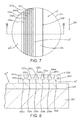
- a small portion of the chip 15 " is circumscribed by a dashed circle 235. The portion circumscribed by the dashed circle 235 will be shown at much greater magnification in FIG. 7 so that additional features of the outer frame 75" may be illustrated.
- FIG. 7 is the portion of FIG. 6 circumscribed by the dashed oval 235 shown at greater magnification.
- the outer frame 75" is visible along with the portion of the channel 85" and the edge 240 of the chip 15 ".
- the portion of the semiconductor chip 15 " positioned to the right of the frame 75 " and labeled 245 may consist of a passivation stack of the type depicted in FIGS. 3 and 4 and labeled 55.
- the outer frame 75" may include a plurality of grooves 250a, 250b, 250c, 250d, 250e and 250f.
- the purpose of the grooves 250a, 250b, 250c, 250d, 250e and 250f is to provide spaces in which a subsequently deposited underfill material may invade and form plural micro-mechanical joints between the underfill with the outer frame 75 ".
- the number of grooves 250a, 250b, 250c, 250d, 250e and 250f is largely a matter of design discretion and may number one or more.
- the grooves 250a, 250b, 250c, 250d, 250e and 250f and the outer frame 75" are depicted as being continuous along the axis 253, it should be understood that the grooves 250a, 250b, 250c, 250d, 250e and 250f and the outer frame 75" could be fabricated as respective groups of segments that extend along the axis 253.
- the grooves 250a, 250b, 250c, 250d, 250e and 250f may extend around the entire perimeter of the outer frame 75 ".
- a corresponding groove or set of grooves may be provided in the inner frame 70" as well.
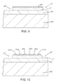
- FIG. 8 is a sectional view of FIG. 7 taken at section 8-8.
- the semiconductor chip 15 " is depicted with a single monolithic structure 255 upon which the passivation stack 245 is formed.
- the monolithic structure 255 may in fact consist of the multiple layers, for example, 45, 47, 50 and 55 depicted in FIGS. 3 and 4 .
- the grooves 250a, 250b, 250c, 250d, 250e and 250f may consist of upper portions 255a, 255b, 255c, 255d, 255e and 255f and relatively wider lower portions 260a, 260b, 260c, 260d, 260e and 260f.
- underfill (not shown) invades the grooves 250a, 250b, 250c, 250d, 250e and 250f and hardens during a curing process, the respective upper portions 255a, 255b, 255c, 255d, 255e and 255f and lower portions 260a, 260b, 260c, 260d, 260e and 260f will establish mechanical joints not unlike several small tongue and groove joints.
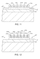
- FIGS. 9, 10 , 11, 12 and 13 An exemplary method for fabricating the grooves 250a, 250b, 250c, 250d, 250e and 250f will now be described in conjunction with FIGS. 9, 10 , 11, 12 and 13 .
- the description will focus on the outer frame 75 ", but will applicable to the inner frame 70" shown in FIG. 6 as well.
- the outer frame 75 " and channel 85 " may be fabricated by well-known material deposition and lithography steps.
- a sacrificial oxide layer 265 is formed on the outer frame 75 " by way of well-known chemical vapor deposition or other material deposition techniques. Referring now to FIG.
- the sacrificial oxide layer 265 is appropriately masked and subjected to an etch process to define plural segments 270a, 270b, 270c, 270d, 270e and 270f.
- This etch may be a dry etch or wet etch process.
- the channel 85 ", the passivation stack 245 on the main chip portion 255 and the outer frame 75 " may be masked during the etch to prevent attack.
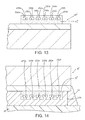
- the outer frame 75" is increased in height by way of a material deposition step that covers the previously formed segments 270a, 270b, 270c, 270d, 270e and 270f of sacrificial oxide. This may be accomplished by merely depositing an additional volume of the polymer material. Some of the additional polymer material 275 may be actually deposited into the channel 85 " and on other portions of the passivation stack 245. This additional polymer material 275 may be subsequently removed by appropriate masking and etching if desired. Referring now to FIG.
- the outer frame 75 " may be appropriately masked and directionally etched to establish the upper trench portions 255a, 255b, 255c, 255d, 255e and 255f in the frame 75" that extend down to the sacrificial oxide segments 270a, 270b, 270c, 270d, 270e and 270f.
- the etch may be used to clear excess polymer material from portions of the semiconductor chip 15", such as the channel 85 " and other portions of the passivation stack 245.
- a wet etch process is performed to remove the sacrificial oxide segments and thus leave the aforementioned grooves 250a, 250b, 250c, 250d, 250e and 250f in the outer frame 75 ".
- the upper trench portions 255a, 255b, 255c, 255d, 255e and 255f enable the wet etchant solution to reach and etch the sacrificial oxide segments 270a, 270b, 270c, 270d, 270e and 270f.
- the patterning of the inner and outer frames of any of the disclosed embodiments may be done while the semiconductor chip 15" is part of a larger semiconductor workpiece, such as a wafer, or after singulation if desired. The same is true for any of the embodiments disclosed herein.
- FIG. 14 depicts the semiconductor chip 15 " flip-chip mounted to the package substrate 20 and subsequent to the deposition of the underfill material 30.
- the semiconductor chip 15 " Prior to the underfill 30 deposition, the semiconductor chip 15 " is moved into position relative to the substrate 20 and, for example, a controlled collapse and reflow process is performed to establish plural solder joints, an example of which is labeled 105 in FIG. 3 .
- the underfill material 30 may be deposited and capillary action used to spread the underfill through an interface 275 between the semiconductor chip 15 " and the substrate 20.
- a flowless underfill process may be used in which the underfill material is deposited on the substrate 20 prior to the bumping.
- the underfill 30 invades the grooves 250a, 250b, 250c, 250d, 250e and 250f to form a plurality of micro-mechanical joints with the outer frame 75".
- These T-shaped joints provide both a structural joint as well as chemical bonding between the underfill 30 and the outer frame 75 ".
- the skilled artisan will appreciate that the number and spacing of the grooves 250a, 250b, 250c, 250d, 250e and 250f may be varied greatly depending upon the available process, minimum feature size and lithography techniques, etc.
Landscapes
- Engineering & Computer Science (AREA)
- Computer Hardware Design (AREA)
- Microelectronics & Electronic Packaging (AREA)
- Power Engineering (AREA)
- Physics & Mathematics (AREA)
- Condensed Matter Physics & Semiconductors (AREA)
- General Physics & Mathematics (AREA)
- Manufacturing & Machinery (AREA)
- Structures Or Materials For Encapsulating Or Coating Semiconductor Devices Or Solid State Devices (AREA)
- Encapsulation Of And Coatings For Semiconductor Or Solid State Devices (AREA)
- Wire Bonding (AREA)
Applications Claiming Priority (2)
| Application Number | Priority Date | Filing Date | Title |
|---|---|---|---|
| US12/388,092 US7897433B2 (en) | 2009-02-18 | 2009-02-18 | Semiconductor chip with reinforcement layer and method of making the same |
| PCT/US2010/024462 WO2010096473A2 (en) | 2009-02-18 | 2010-02-17 | Semiconductor chip with reinforcement layer |
Publications (2)
| Publication Number | Publication Date |
|---|---|
| EP2399284A2 EP2399284A2 (en) | 2011-12-28 |
| EP2399284B1 true EP2399284B1 (en) | 2015-06-17 |
Family
ID=42224974
Family Applications (1)
| Application Number | Title | Priority Date | Filing Date |
|---|---|---|---|
| EP10704716.9A Not-in-force EP2399284B1 (en) | 2009-02-18 | 2010-02-17 | Semiconductor chip with reinforcement layer |
Country Status (7)
Families Citing this family (14)
| Publication number | Priority date | Publication date | Assignee | Title |
|---|---|---|---|---|
| US8058108B2 (en) | 2010-03-10 | 2011-11-15 | Ati Technologies Ulc | Methods of forming semiconductor chip underfill anchors |
| US8476115B2 (en) | 2011-05-03 | 2013-07-02 | Stats Chippac, Ltd. | Semiconductor device and method of mounting cover to semiconductor die and interposer with adhesive material |
| US8624404B1 (en) | 2012-06-25 | 2014-01-07 | Advanced Micro Devices, Inc. | Integrated circuit package having offset vias |
| US8937009B2 (en) | 2013-04-25 | 2015-01-20 | International Business Machines Corporation | Far back end of the line metallization method and structures |
| TWI467711B (zh) * | 2013-09-10 | 2015-01-01 | Chipbond Technology Corp | 半導體結構 |
| US9466547B1 (en) | 2015-06-09 | 2016-10-11 | Globalfoundries Inc. | Passivation layer topography |
| US9589920B2 (en) * | 2015-07-01 | 2017-03-07 | Zhuhai Advanced Chip Carriers & Electronic Substrate Solutions Technologies Co. Ltd. | Chip package |
| US9779940B2 (en) * | 2015-07-01 | 2017-10-03 | Zhuahai Advanced Chip Carriers & Electronic Substrate Solutions Technologies Co. Ltd. | Chip package |
| US20200251683A1 (en) * | 2019-01-31 | 2020-08-06 | Wuhan China Star Optoelectronics Semiconductor Display Technology Co., Ltd. | Organic light emitting diode display panel and preparation method thereof |
| EP3800660B1 (en) | 2019-10-02 | 2025-02-19 | STMicroelectronics S.r.l. | Silicon carbide power device with improved robustness and corresponding manufacturing process |
| US11990408B2 (en) * | 2020-03-27 | 2024-05-21 | Intel Corporation | WLCSP reliability improvement for package edges including package shielding |
| KR102798789B1 (ko) | 2020-07-09 | 2025-04-22 | 삼성전자주식회사 | 반도체 패키지 |
| CN114141614A (zh) | 2020-09-04 | 2022-03-04 | 意法半导体股份有限公司 | 电子设备元件制造方法、相关元件、电子设备和电子装置 |
| JP2022043997A (ja) | 2020-09-04 | 2022-03-16 | エスティーマイクロエレクトロニクス エス.アール.エル. | 信頼性を改善した電子装置の要素の製造方法、及び関連要素、電子装置、及び電子機器 |
Citations (5)
| Publication number | Priority date | Publication date | Assignee | Title |
|---|---|---|---|---|
| JPH03133161A (ja) * | 1989-10-19 | 1991-06-06 | Toshiba Corp | 半導体装置 |
| JP2000315752A (ja) * | 1999-04-28 | 2000-11-14 | Shinko Electric Ind Co Ltd | 半導体装置及びその製造方法 |
| US20060012012A1 (en) * | 2004-07-15 | 2006-01-19 | Ping-Wei Wang | Semiconductor device with crack prevention ring and method of manufacture thereof |
| JP2006318989A (ja) * | 2005-05-10 | 2006-11-24 | Matsushita Electric Ind Co Ltd | 半導体装置 |
| US20070120269A1 (en) * | 2005-11-30 | 2007-05-31 | Advanced Semiconductor Engineering, Inc. | Flip chip package and manufacturing method of the same |
Family Cites Families (22)
| Publication number | Priority date | Publication date | Assignee | Title |
|---|---|---|---|---|
| US5861658A (en) * | 1996-10-03 | 1999-01-19 | International Business Machines Corporation | Inorganic seal for encapsulation of an organic layer and method for making the same |
| US6022791A (en) * | 1997-10-15 | 2000-02-08 | International Business Machines Corporation | Chip crack stop |
| US6324069B1 (en) * | 1997-10-29 | 2001-11-27 | Hestia Technologies, Inc. | Chip package with molded underfill |
| US6049124A (en) * | 1997-12-10 | 2000-04-11 | Intel Corporation | Semiconductor package |
| JP2000269386A (ja) * | 1999-03-15 | 2000-09-29 | Texas Instr Japan Ltd | 半導体装置 |
| US6122171A (en) * | 1999-07-30 | 2000-09-19 | Micron Technology, Inc. | Heat sink chip package and method of making |
| US7267148B2 (en) * | 1999-08-10 | 2007-09-11 | Michelin Recherche Et Technique S.A. | Measurement of adherence between a vehicle wheel and the roadway |
| JP2002270735A (ja) * | 2001-03-13 | 2002-09-20 | Nec Corp | 半導体装置及びその製造方法 |
| JP4088120B2 (ja) * | 2002-08-12 | 2008-05-21 | 株式会社ルネサステクノロジ | 半導体装置 |
| JP2004200532A (ja) * | 2002-12-20 | 2004-07-15 | Renesas Technology Corp | 半導体装置およびその製造方法 |
| JP4346333B2 (ja) * | 2003-03-26 | 2009-10-21 | 新光電気工業株式会社 | 半導体素子を内蔵した多層回路基板の製造方法 |
| JP2006041239A (ja) * | 2004-07-28 | 2006-02-09 | Toshiba Corp | 配線基板及び磁気ディスク装置 |
| DE102005003390B4 (de) * | 2005-01-24 | 2007-09-13 | Qimonda Ag | Substrat für ein FBGA-Halbleiterbauelement |
| US20060278957A1 (en) * | 2005-06-09 | 2006-12-14 | Zong-Huei Lin | Fabrication of semiconductor integrated circuit chips |
| CN100461408C (zh) * | 2005-09-28 | 2009-02-11 | 中芯国际集成电路制造(上海)有限公司 | 带有密封环拐角结构的集成电路器件 |
| JP5118300B2 (ja) * | 2005-12-20 | 2013-01-16 | 富士通セミコンダクター株式会社 | 半導体装置及びその製造方法 |
| JP2008078382A (ja) * | 2006-09-21 | 2008-04-03 | Toshiba Corp | 半導体装置とその製造方法 |
| US8736039B2 (en) * | 2006-10-06 | 2014-05-27 | Taiwan Semiconductor Manufacturing Co., Ltd. | Stacked structures and methods of forming stacked structures |
| US20080169555A1 (en) * | 2007-01-16 | 2008-07-17 | Ati Technologies Ulc | Anchor structure for an integrated circuit |
| US7732932B2 (en) * | 2007-08-03 | 2010-06-08 | International Business Machines Corporation | Semiconductor chips with crack stop regions for reducing crack propagation from chip edges/corners |
| KR100910233B1 (ko) * | 2008-01-02 | 2009-07-31 | 주식회사 하이닉스반도체 | 적층 웨이퍼 레벨 패키지 |
| US8441804B2 (en) * | 2008-07-25 | 2013-05-14 | Infineon Technologies Ag | Semiconductor device and method of manufacturing a semiconductor device |
-
2009
- 2009-02-18 US US12/388,092 patent/US7897433B2/en active Active
-
2010
- 2010-02-17 CN CN201080008014.8A patent/CN102318051B/zh active Active
- 2010-02-17 SG SG2011053386A patent/SG173447A1/en unknown
- 2010-02-17 EP EP10704716.9A patent/EP2399284B1/en not_active Not-in-force
- 2010-02-17 KR KR1020117021554A patent/KR101308100B1/ko active Active
- 2010-02-17 JP JP2011550323A patent/JP5576885B2/ja active Active
- 2010-02-17 WO PCT/US2010/024462 patent/WO2010096473A2/en active Application Filing
Patent Citations (5)
| Publication number | Priority date | Publication date | Assignee | Title |
|---|---|---|---|---|
| JPH03133161A (ja) * | 1989-10-19 | 1991-06-06 | Toshiba Corp | 半導体装置 |
| JP2000315752A (ja) * | 1999-04-28 | 2000-11-14 | Shinko Electric Ind Co Ltd | 半導体装置及びその製造方法 |
| US20060012012A1 (en) * | 2004-07-15 | 2006-01-19 | Ping-Wei Wang | Semiconductor device with crack prevention ring and method of manufacture thereof |
| JP2006318989A (ja) * | 2005-05-10 | 2006-11-24 | Matsushita Electric Ind Co Ltd | 半導体装置 |
| US20070120269A1 (en) * | 2005-11-30 | 2007-05-31 | Advanced Semiconductor Engineering, Inc. | Flip chip package and manufacturing method of the same |
Also Published As
| Publication number | Publication date |
|---|---|
| KR20110126707A (ko) | 2011-11-23 |
| EP2399284A2 (en) | 2011-12-28 |
| WO2010096473A2 (en) | 2010-08-26 |
| KR101308100B1 (ko) | 2013-09-12 |
| CN102318051B (zh) | 2014-02-26 |
| US7897433B2 (en) | 2011-03-01 |
| CN102318051A (zh) | 2012-01-11 |
| WO2010096473A3 (en) | 2011-02-03 |
| US20100207281A1 (en) | 2010-08-19 |
| JP2012518282A (ja) | 2012-08-09 |
| JP5576885B2 (ja) | 2014-08-20 |
| SG173447A1 (en) | 2011-09-29 |
Similar Documents
| Publication | Publication Date | Title |
|---|---|---|
| EP2399284B1 (en) | Semiconductor chip with reinforcement layer | |
| US11037819B2 (en) | Wafer level chip scale packaging intermediate structure apparatus and method | |
| KR101903903B1 (ko) | 감소된 두께를 갖는 디바이스 패키지 및 그 형성 방법 | |
| US11913121B2 (en) | Fabrication method of substrate having electrical interconnection structures | |
| US6818998B2 (en) | Stacked chip package having upper chip provided with trenches and method of manufacturing the same | |
| US8124448B2 (en) | Semiconductor chip with crack deflection structure | |
| US7737563B2 (en) | Semiconductor chip with reinforcement structure | |
| KR20040083796A (ko) | 웨이퍼 레벨 칩 스케일 패키지, 그를 적층한 적층 패키지및 그 제조 방법 | |
| US12148692B2 (en) | Semiconductor package and manufacturing method thereof | |
| US12051616B2 (en) | Wafer level chip scale packaging intermediate structure apparatus and method | |
| US11201097B2 (en) | Method of manufacture of a semiconductor device | |
| CN109216215B (zh) | 半导体器件和制造方法 | |
| KR20170052466A (ko) | 캐비티를 갖는 폴리머-기반 반도체 구조체 | |
| JP2009033153A (ja) | 半導体素子パッケージ用の相互接続構造およびその方法 | |
| KR101013545B1 (ko) | 스택 패키지 및 그의 제조방법 | |
| CN222530419U (zh) | 包括虚设条的封装 | |
| KR100842916B1 (ko) | 스택 패키지의 제조방법 |
Legal Events
| Date | Code | Title | Description |
|---|---|---|---|
| PUAI | Public reference made under article 153(3) epc to a published international application that has entered the european phase |
Free format text: ORIGINAL CODE: 0009012 |
|
| 17P | Request for examination filed |
Effective date: 20110803 |
|
| AK | Designated contracting states |
Kind code of ref document: A2 Designated state(s): AT BE BG CH CY CZ DE DK EE ES FI FR GB GR HR HU IE IS IT LI LT LU LV MC MK MT NL NO PL PT RO SE SI SK SM TR |
|
| RIN1 | Information on inventor provided before grant (corrected) |
Inventor name: SU, MICHAEL Inventor name: KUECHENMEISTER, FRANK Inventor name: BRAVO, JAIME |
|
| DAX | Request for extension of the european patent (deleted) | ||
| 17Q | First examination report despatched |
Effective date: 20121211 |
|
| GRAP | Despatch of communication of intention to grant a patent |
Free format text: ORIGINAL CODE: EPIDOSNIGR1 |
|
| INTG | Intention to grant announced |
Effective date: 20150120 |
|
| GRAS | Grant fee paid |
Free format text: ORIGINAL CODE: EPIDOSNIGR3 |
|
| GRAA | (expected) grant |
Free format text: ORIGINAL CODE: 0009210 |
|
| AK | Designated contracting states |
Kind code of ref document: B1 Designated state(s): AT BE BG CH CY CZ DE DK EE ES FI FR GB GR HR HU IE IS IT LI LT LU LV MC MK MT NL NO PL PT RO SE SI SK SM TR |
|
| REG | Reference to a national code |
Ref country code: GB Ref legal event code: FG4D |
|
| REG | Reference to a national code |
Ref country code: CH Ref legal event code: EP |
|
| REG | Reference to a national code |
Ref country code: AT Ref legal event code: REF Ref document number: 732337 Country of ref document: AT Kind code of ref document: T Effective date: 20150715 |
|
| REG | Reference to a national code |
Ref country code: IE Ref legal event code: FG4D |
|
| REG | Reference to a national code |
Ref country code: DE Ref legal event code: R096 Ref document number: 602010025272 Country of ref document: DE |
|
| PG25 | Lapsed in a contracting state [announced via postgrant information from national office to epo] |
Ref country code: LT Free format text: LAPSE BECAUSE OF FAILURE TO SUBMIT A TRANSLATION OF THE DESCRIPTION OR TO PAY THE FEE WITHIN THE PRESCRIBED TIME-LIMIT Effective date: 20150617 Ref country code: HR Free format text: LAPSE BECAUSE OF FAILURE TO SUBMIT A TRANSLATION OF THE DESCRIPTION OR TO PAY THE FEE WITHIN THE PRESCRIBED TIME-LIMIT Effective date: 20150617 Ref country code: NO Free format text: LAPSE BECAUSE OF FAILURE TO SUBMIT A TRANSLATION OF THE DESCRIPTION OR TO PAY THE FEE WITHIN THE PRESCRIBED TIME-LIMIT Effective date: 20150917 Ref country code: FI Free format text: LAPSE BECAUSE OF FAILURE TO SUBMIT A TRANSLATION OF THE DESCRIPTION OR TO PAY THE FEE WITHIN THE PRESCRIBED TIME-LIMIT Effective date: 20150617 |
|
| REG | Reference to a national code |
Ref country code: AT Ref legal event code: MK05 Ref document number: 732337 Country of ref document: AT Kind code of ref document: T Effective date: 20150617 |
|
| REG | Reference to a national code |
Ref country code: LT Ref legal event code: MG4D Ref country code: NL Ref legal event code: MP Effective date: 20150617 |
|
| PG25 | Lapsed in a contracting state [announced via postgrant information from national office to epo] |
Ref country code: GR Free format text: LAPSE BECAUSE OF FAILURE TO SUBMIT A TRANSLATION OF THE DESCRIPTION OR TO PAY THE FEE WITHIN THE PRESCRIBED TIME-LIMIT Effective date: 20150918 Ref country code: BG Free format text: LAPSE BECAUSE OF FAILURE TO SUBMIT A TRANSLATION OF THE DESCRIPTION OR TO PAY THE FEE WITHIN THE PRESCRIBED TIME-LIMIT Effective date: 20150917 Ref country code: LV Free format text: LAPSE BECAUSE OF FAILURE TO SUBMIT A TRANSLATION OF THE DESCRIPTION OR TO PAY THE FEE WITHIN THE PRESCRIBED TIME-LIMIT Effective date: 20150617 |
|
| PG25 | Lapsed in a contracting state [announced via postgrant information from national office to epo] |
Ref country code: EE Free format text: LAPSE BECAUSE OF FAILURE TO SUBMIT A TRANSLATION OF THE DESCRIPTION OR TO PAY THE FEE WITHIN THE PRESCRIBED TIME-LIMIT Effective date: 20150617 |
|
| PG25 | Lapsed in a contracting state [announced via postgrant information from national office to epo] |
Ref country code: SK Free format text: LAPSE BECAUSE OF FAILURE TO SUBMIT A TRANSLATION OF THE DESCRIPTION OR TO PAY THE FEE WITHIN THE PRESCRIBED TIME-LIMIT Effective date: 20150617 Ref country code: PL Free format text: LAPSE BECAUSE OF FAILURE TO SUBMIT A TRANSLATION OF THE DESCRIPTION OR TO PAY THE FEE WITHIN THE PRESCRIBED TIME-LIMIT Effective date: 20150617 Ref country code: ES Free format text: LAPSE BECAUSE OF FAILURE TO SUBMIT A TRANSLATION OF THE DESCRIPTION OR TO PAY THE FEE WITHIN THE PRESCRIBED TIME-LIMIT Effective date: 20150617 Ref country code: PT Free format text: LAPSE BECAUSE OF FAILURE TO SUBMIT A TRANSLATION OF THE DESCRIPTION OR TO PAY THE FEE WITHIN THE PRESCRIBED TIME-LIMIT Effective date: 20151019 Ref country code: IS Free format text: LAPSE BECAUSE OF FAILURE TO SUBMIT A TRANSLATION OF THE DESCRIPTION OR TO PAY THE FEE WITHIN THE PRESCRIBED TIME-LIMIT Effective date: 20151017 Ref country code: AT Free format text: LAPSE BECAUSE OF FAILURE TO SUBMIT A TRANSLATION OF THE DESCRIPTION OR TO PAY THE FEE WITHIN THE PRESCRIBED TIME-LIMIT Effective date: 20150617 Ref country code: RO Free format text: LAPSE BECAUSE OF NON-PAYMENT OF DUE FEES Effective date: 20150617 Ref country code: CZ Free format text: LAPSE BECAUSE OF FAILURE TO SUBMIT A TRANSLATION OF THE DESCRIPTION OR TO PAY THE FEE WITHIN THE PRESCRIBED TIME-LIMIT Effective date: 20150617 |
|
| REG | Reference to a national code |
Ref country code: DE Ref legal event code: R097 Ref document number: 602010025272 Country of ref document: DE |
|
| PLBE | No opposition filed within time limit |
Free format text: ORIGINAL CODE: 0009261 |
|
| STAA | Information on the status of an ep patent application or granted ep patent |
Free format text: STATUS: NO OPPOSITION FILED WITHIN TIME LIMIT |
|
| PG25 | Lapsed in a contracting state [announced via postgrant information from national office to epo] |
Ref country code: IT Free format text: LAPSE BECAUSE OF FAILURE TO SUBMIT A TRANSLATION OF THE DESCRIPTION OR TO PAY THE FEE WITHIN THE PRESCRIBED TIME-LIMIT Effective date: 20150617 Ref country code: DK Free format text: LAPSE BECAUSE OF FAILURE TO SUBMIT A TRANSLATION OF THE DESCRIPTION OR TO PAY THE FEE WITHIN THE PRESCRIBED TIME-LIMIT Effective date: 20150617 |
|
| 26N | No opposition filed |
Effective date: 20160318 |
|
| PG25 | Lapsed in a contracting state [announced via postgrant information from national office to epo] |
Ref country code: BE Free format text: LAPSE BECAUSE OF NON-PAYMENT OF DUE FEES Effective date: 20160229 |
|
| PG25 | Lapsed in a contracting state [announced via postgrant information from national office to epo] |
Ref country code: SI Free format text: LAPSE BECAUSE OF FAILURE TO SUBMIT A TRANSLATION OF THE DESCRIPTION OR TO PAY THE FEE WITHIN THE PRESCRIBED TIME-LIMIT Effective date: 20150617 |
|
| REG | Reference to a national code |
Ref country code: DE Ref legal event code: R119 Ref document number: 602010025272 Country of ref document: DE |
|
| PG25 | Lapsed in a contracting state [announced via postgrant information from national office to epo] |
Ref country code: MC Free format text: LAPSE BECAUSE OF FAILURE TO SUBMIT A TRANSLATION OF THE DESCRIPTION OR TO PAY THE FEE WITHIN THE PRESCRIBED TIME-LIMIT Effective date: 20150617 Ref country code: LU Free format text: LAPSE BECAUSE OF FAILURE TO SUBMIT A TRANSLATION OF THE DESCRIPTION OR TO PAY THE FEE WITHIN THE PRESCRIBED TIME-LIMIT Effective date: 20160217 |
|
| REG | Reference to a national code |
Ref country code: CH Ref legal event code: PL |
|
| GBPC | Gb: european patent ceased through non-payment of renewal fee |
Effective date: 20160217 |
|
| PG25 | Lapsed in a contracting state [announced via postgrant information from national office to epo] |
Ref country code: LI Free format text: LAPSE BECAUSE OF NON-PAYMENT OF DUE FEES Effective date: 20160229 Ref country code: CH Free format text: LAPSE BECAUSE OF NON-PAYMENT OF DUE FEES Effective date: 20160229 |
|
| REG | Reference to a national code |
Ref country code: FR Ref legal event code: ST Effective date: 20161028 |
|
| REG | Reference to a national code |
Ref country code: IE Ref legal event code: MM4A |
|
| PG25 | Lapsed in a contracting state [announced via postgrant information from national office to epo] |
Ref country code: BE Free format text: LAPSE BECAUSE OF FAILURE TO SUBMIT A TRANSLATION OF THE DESCRIPTION OR TO PAY THE FEE WITHIN THE PRESCRIBED TIME-LIMIT Effective date: 20150617 |
|
| PG25 | Lapsed in a contracting state [announced via postgrant information from national office to epo] |
Ref country code: DE Free format text: LAPSE BECAUSE OF NON-PAYMENT OF DUE FEES Effective date: 20160901 Ref country code: FR Free format text: LAPSE BECAUSE OF NON-PAYMENT OF DUE FEES Effective date: 20160229 Ref country code: GB Free format text: LAPSE BECAUSE OF NON-PAYMENT OF DUE FEES Effective date: 20160217 Ref country code: IE Free format text: LAPSE BECAUSE OF NON-PAYMENT OF DUE FEES Effective date: 20160217 |
|
| PG25 | Lapsed in a contracting state [announced via postgrant information from national office to epo] |
Ref country code: SE Free format text: LAPSE BECAUSE OF FAILURE TO SUBMIT A TRANSLATION OF THE DESCRIPTION OR TO PAY THE FEE WITHIN THE PRESCRIBED TIME-LIMIT Effective date: 20150617 Ref country code: NL Free format text: LAPSE BECAUSE OF FAILURE TO SUBMIT A TRANSLATION OF THE DESCRIPTION OR TO PAY THE FEE WITHIN THE PRESCRIBED TIME-LIMIT Effective date: 20150617 |
|
| PG25 | Lapsed in a contracting state [announced via postgrant information from national office to epo] |
Ref country code: MT Free format text: LAPSE BECAUSE OF FAILURE TO SUBMIT A TRANSLATION OF THE DESCRIPTION OR TO PAY THE FEE WITHIN THE PRESCRIBED TIME-LIMIT Effective date: 20150617 |
|
| PG25 | Lapsed in a contracting state [announced via postgrant information from national office to epo] |
Ref country code: HU Free format text: LAPSE BECAUSE OF FAILURE TO SUBMIT A TRANSLATION OF THE DESCRIPTION OR TO PAY THE FEE WITHIN THE PRESCRIBED TIME-LIMIT; INVALID AB INITIO Effective date: 20100217 Ref country code: CY Free format text: LAPSE BECAUSE OF FAILURE TO SUBMIT A TRANSLATION OF THE DESCRIPTION OR TO PAY THE FEE WITHIN THE PRESCRIBED TIME-LIMIT Effective date: 20150617 Ref country code: SM Free format text: LAPSE BECAUSE OF FAILURE TO SUBMIT A TRANSLATION OF THE DESCRIPTION OR TO PAY THE FEE WITHIN THE PRESCRIBED TIME-LIMIT Effective date: 20150617 |
|
| PG25 | Lapsed in a contracting state [announced via postgrant information from national office to epo] |
Ref country code: TR Free format text: LAPSE BECAUSE OF FAILURE TO SUBMIT A TRANSLATION OF THE DESCRIPTION OR TO PAY THE FEE WITHIN THE PRESCRIBED TIME-LIMIT Effective date: 20150617 Ref country code: MK Free format text: LAPSE BECAUSE OF FAILURE TO SUBMIT A TRANSLATION OF THE DESCRIPTION OR TO PAY THE FEE WITHIN THE PRESCRIBED TIME-LIMIT Effective date: 20150617 Ref country code: MT Free format text: LAPSE BECAUSE OF FAILURE TO SUBMIT A TRANSLATION OF THE DESCRIPTION OR TO PAY THE FEE WITHIN THE PRESCRIBED TIME-LIMIT Effective date: 20160229 |
|
| P01 | Opt-out of the competence of the unified patent court (upc) registered |
Effective date: 20230530 |