EP2397749A2 - Lichtemittierende Vorrichtung und Beleuchtungsvorrichtung - Google Patents
Lichtemittierende Vorrichtung und Beleuchtungsvorrichtung Download PDFInfo
- Publication number
- EP2397749A2 EP2397749A2 EP11170336A EP11170336A EP2397749A2 EP 2397749 A2 EP2397749 A2 EP 2397749A2 EP 11170336 A EP11170336 A EP 11170336A EP 11170336 A EP11170336 A EP 11170336A EP 2397749 A2 EP2397749 A2 EP 2397749A2
- Authority
- EP
- European Patent Office
- Prior art keywords
- light
- emitting elements
- substrate
- emitting
- feed line
- Prior art date
- Legal status (The legal status is an assumption and is not a legal conclusion. Google has not performed a legal analysis and makes no representation as to the accuracy of the status listed.)
- Withdrawn
Links
- 239000000758 substrate Substances 0.000 claims abstract description 81
- 238000007789 sealing Methods 0.000 claims abstract description 13
- 230000002596 correlated effect Effects 0.000 claims description 16
- 239000010410 layer Substances 0.000 description 58
- OAICVXFJPJFONN-UHFFFAOYSA-N Phosphorus Chemical compound [P] OAICVXFJPJFONN-UHFFFAOYSA-N 0.000 description 44
- 238000005286 illumination Methods 0.000 description 10
- 239000004020 conductor Substances 0.000 description 8
- PXHVJJICTQNCMI-UHFFFAOYSA-N Nickel Chemical compound [Ni] PXHVJJICTQNCMI-UHFFFAOYSA-N 0.000 description 6
- 239000003086 colorant Substances 0.000 description 6
- 238000009713 electroplating Methods 0.000 description 6
- 239000000463 material Substances 0.000 description 5
- 238000010586 diagram Methods 0.000 description 4
- 239000010931 gold Substances 0.000 description 4
- 238000000034 method Methods 0.000 description 4
- 150000004767 nitrides Chemical class 0.000 description 4
- 230000005855 radiation Effects 0.000 description 4
- 239000004065 semiconductor Substances 0.000 description 4
- 229920003002 synthetic resin Polymers 0.000 description 4
- 239000000057 synthetic resin Substances 0.000 description 4
- RYGMFSIKBFXOCR-UHFFFAOYSA-N Copper Chemical compound [Cu] RYGMFSIKBFXOCR-UHFFFAOYSA-N 0.000 description 3
- BQCADISMDOOEFD-UHFFFAOYSA-N Silver Chemical compound [Ag] BQCADISMDOOEFD-UHFFFAOYSA-N 0.000 description 3
- 229920002050 silicone resin Polymers 0.000 description 3
- 229910052709 silver Inorganic materials 0.000 description 3
- 239000004332 silver Substances 0.000 description 3
- 239000002344 surface layer Substances 0.000 description 3
- 229910019990 cerium-doped yttrium aluminum garnet Inorganic materials 0.000 description 2
- 239000010949 copper Substances 0.000 description 2
- 239000011889 copper foil Substances 0.000 description 2
- 238000000605 extraction Methods 0.000 description 2
- PCHJSUWPFVWCPO-UHFFFAOYSA-N gold Chemical compound [Au] PCHJSUWPFVWCPO-UHFFFAOYSA-N 0.000 description 2
- 229910052737 gold Inorganic materials 0.000 description 2
- 238000010030 laminating Methods 0.000 description 2
- 238000012986 modification Methods 0.000 description 2
- 230000004048 modification Effects 0.000 description 2
- 229910052759 nickel Inorganic materials 0.000 description 2
- XUIMIQQOPSSXEZ-UHFFFAOYSA-N Silicon Chemical compound [Si] XUIMIQQOPSSXEZ-UHFFFAOYSA-N 0.000 description 1
- 239000000853 adhesive Substances 0.000 description 1
- 230000001070 adhesive effect Effects 0.000 description 1
- XAGFODPZIPBFFR-UHFFFAOYSA-N aluminium Chemical compound [Al] XAGFODPZIPBFFR-UHFFFAOYSA-N 0.000 description 1
- 229910052782 aluminium Inorganic materials 0.000 description 1
- 239000000919 ceramic Substances 0.000 description 1
- 230000000295 complement effect Effects 0.000 description 1
- 229910052802 copper Inorganic materials 0.000 description 1
- 230000000875 corresponding effect Effects 0.000 description 1
- 230000003247 decreasing effect Effects 0.000 description 1
- 230000000694 effects Effects 0.000 description 1
- 239000003822 epoxy resin Substances 0.000 description 1
- 239000011521 glass Substances 0.000 description 1
- 238000013007 heat curing Methods 0.000 description 1
- 239000011810 insulating material Substances 0.000 description 1
- 238000009413 insulation Methods 0.000 description 1
- 239000011159 matrix material Substances 0.000 description 1
- 230000007935 neutral effect Effects 0.000 description 1
- 238000004806 packaging method and process Methods 0.000 description 1
- 238000007747 plating Methods 0.000 description 1
- 229920000647 polyepoxide Polymers 0.000 description 1
- 229920005989 resin Polymers 0.000 description 1
- 239000011347 resin Substances 0.000 description 1
- 229910052594 sapphire Inorganic materials 0.000 description 1
- 239000010980 sapphire Substances 0.000 description 1
- 229910052710 silicon Inorganic materials 0.000 description 1
- 239000010703 silicon Substances 0.000 description 1
- 238000006467 substitution reaction Methods 0.000 description 1
Images


Classifications
-
- H—ELECTRICITY
- H05—ELECTRIC TECHNIQUES NOT OTHERWISE PROVIDED FOR
- H05K—PRINTED CIRCUITS; CASINGS OR CONSTRUCTIONAL DETAILS OF ELECTRIC APPARATUS; MANUFACTURE OF ASSEMBLAGES OF ELECTRICAL COMPONENTS
- H05K1/00—Printed circuits
- H05K1/02—Details
- H05K1/0201—Thermal arrangements, e.g. for cooling, heating or preventing overheating
- H05K1/0203—Cooling of mounted components
- H05K1/0209—External configuration of printed circuit board adapted for heat dissipation, e.g. lay-out of conductors, coatings
-
- F—MECHANICAL ENGINEERING; LIGHTING; HEATING; WEAPONS; BLASTING
- F21—LIGHTING
- F21S—NON-PORTABLE LIGHTING DEVICES; SYSTEMS THEREOF; VEHICLE LIGHTING DEVICES SPECIALLY ADAPTED FOR VEHICLE EXTERIORS
- F21S8/00—Lighting devices intended for fixed installation
- F21S8/04—Lighting devices intended for fixed installation intended only for mounting on a ceiling or the like overhead structures
-
- H—ELECTRICITY
- H01—ELECTRIC ELEMENTS
- H01L—SEMICONDUCTOR DEVICES NOT COVERED BY CLASS H10
- H01L25/00—Assemblies consisting of a plurality of individual semiconductor or other solid state devices ; Multistep manufacturing processes thereof
- H01L25/03—Assemblies consisting of a plurality of individual semiconductor or other solid state devices ; Multistep manufacturing processes thereof all the devices being of a type provided for in the same subgroup of groups H01L27/00 - H01L33/00, or in a single subclass of H10K, H10N, e.g. assemblies of rectifier diodes
- H01L25/04—Assemblies consisting of a plurality of individual semiconductor or other solid state devices ; Multistep manufacturing processes thereof all the devices being of a type provided for in the same subgroup of groups H01L27/00 - H01L33/00, or in a single subclass of H10K, H10N, e.g. assemblies of rectifier diodes the devices not having separate containers
- H01L25/075—Assemblies consisting of a plurality of individual semiconductor or other solid state devices ; Multistep manufacturing processes thereof all the devices being of a type provided for in the same subgroup of groups H01L27/00 - H01L33/00, or in a single subclass of H10K, H10N, e.g. assemblies of rectifier diodes the devices not having separate containers the devices being of a type provided for in group H01L33/00
- H01L25/0753—Assemblies consisting of a plurality of individual semiconductor or other solid state devices ; Multistep manufacturing processes thereof all the devices being of a type provided for in the same subgroup of groups H01L27/00 - H01L33/00, or in a single subclass of H10K, H10N, e.g. assemblies of rectifier diodes the devices not having separate containers the devices being of a type provided for in group H01L33/00 the devices being arranged next to each other
-
- F—MECHANICAL ENGINEERING; LIGHTING; HEATING; WEAPONS; BLASTING
- F21—LIGHTING
- F21S—NON-PORTABLE LIGHTING DEVICES; SYSTEMS THEREOF; VEHICLE LIGHTING DEVICES SPECIALLY ADAPTED FOR VEHICLE EXTERIORS
- F21S2/00—Systems of lighting devices, not provided for in main groups F21S4/00 - F21S10/00 or F21S19/00, e.g. of modular construction
- F21S2/005—Systems of lighting devices, not provided for in main groups F21S4/00 - F21S10/00 or F21S19/00, e.g. of modular construction of modular construction
-
- F—MECHANICAL ENGINEERING; LIGHTING; HEATING; WEAPONS; BLASTING
- F21—LIGHTING
- F21Y—INDEXING SCHEME ASSOCIATED WITH SUBCLASSES F21K, F21L, F21S and F21V, RELATING TO THE FORM OR THE KIND OF THE LIGHT SOURCES OR OF THE COLOUR OF THE LIGHT EMITTED
- F21Y2105/00—Planar light sources
- F21Y2105/10—Planar light sources comprising a two-dimensional array of point-like light-generating elements
-
- F—MECHANICAL ENGINEERING; LIGHTING; HEATING; WEAPONS; BLASTING
- F21—LIGHTING
- F21Y—INDEXING SCHEME ASSOCIATED WITH SUBCLASSES F21K, F21L, F21S and F21V, RELATING TO THE FORM OR THE KIND OF THE LIGHT SOURCES OR OF THE COLOUR OF THE LIGHT EMITTED
- F21Y2115/00—Light-generating elements of semiconductor light sources
- F21Y2115/10—Light-emitting diodes [LED]
-
- H—ELECTRICITY
- H01—ELECTRIC ELEMENTS
- H01L—SEMICONDUCTOR DEVICES NOT COVERED BY CLASS H10
- H01L2224/00—Indexing scheme for arrangements for connecting or disconnecting semiconductor or solid-state bodies and methods related thereto as covered by H01L24/00
- H01L2224/01—Means for bonding being attached to, or being formed on, the surface to be connected, e.g. chip-to-package, die-attach, "first-level" interconnects; Manufacturing methods related thereto
- H01L2224/42—Wire connectors; Manufacturing methods related thereto
- H01L2224/47—Structure, shape, material or disposition of the wire connectors after the connecting process
- H01L2224/48—Structure, shape, material or disposition of the wire connectors after the connecting process of an individual wire connector
- H01L2224/4805—Shape
- H01L2224/4809—Loop shape
- H01L2224/48091—Arched
-
- H—ELECTRICITY
- H01—ELECTRIC ELEMENTS
- H01L—SEMICONDUCTOR DEVICES NOT COVERED BY CLASS H10
- H01L2224/00—Indexing scheme for arrangements for connecting or disconnecting semiconductor or solid-state bodies and methods related thereto as covered by H01L24/00
- H01L2224/01—Means for bonding being attached to, or being formed on, the surface to be connected, e.g. chip-to-package, die-attach, "first-level" interconnects; Manufacturing methods related thereto
- H01L2224/42—Wire connectors; Manufacturing methods related thereto
- H01L2224/47—Structure, shape, material or disposition of the wire connectors after the connecting process
- H01L2224/48—Structure, shape, material or disposition of the wire connectors after the connecting process of an individual wire connector
- H01L2224/481—Disposition
- H01L2224/48135—Connecting between different semiconductor or solid-state bodies, i.e. chip-to-chip
- H01L2224/48137—Connecting between different semiconductor or solid-state bodies, i.e. chip-to-chip the bodies being arranged next to each other, e.g. on a common substrate
-
- H—ELECTRICITY
- H01—ELECTRIC ELEMENTS
- H01L—SEMICONDUCTOR DEVICES NOT COVERED BY CLASS H10
- H01L2224/00—Indexing scheme for arrangements for connecting or disconnecting semiconductor or solid-state bodies and methods related thereto as covered by H01L24/00
- H01L2224/73—Means for bonding being of different types provided for in two or more of groups H01L2224/10, H01L2224/18, H01L2224/26, H01L2224/34, H01L2224/42, H01L2224/50, H01L2224/63, H01L2224/71
- H01L2224/732—Location after the connecting process
- H01L2224/73251—Location after the connecting process on different surfaces
- H01L2224/73265—Layer and wire connectors
-
- H—ELECTRICITY
- H01—ELECTRIC ELEMENTS
- H01L—SEMICONDUCTOR DEVICES NOT COVERED BY CLASS H10
- H01L33/00—Semiconductor devices with at least one potential-jump barrier or surface barrier specially adapted for light emission; Processes or apparatus specially adapted for the manufacture or treatment thereof or of parts thereof; Details thereof
- H01L33/48—Semiconductor devices with at least one potential-jump barrier or surface barrier specially adapted for light emission; Processes or apparatus specially adapted for the manufacture or treatment thereof or of parts thereof; Details thereof characterised by the semiconductor body packages
- H01L33/50—Wavelength conversion elements
-
- H—ELECTRICITY
- H05—ELECTRIC TECHNIQUES NOT OTHERWISE PROVIDED FOR
- H05K—PRINTED CIRCUITS; CASINGS OR CONSTRUCTIONAL DETAILS OF ELECTRIC APPARATUS; MANUFACTURE OF ASSEMBLAGES OF ELECTRICAL COMPONENTS
- H05K1/00—Printed circuits
- H05K1/18—Printed circuits structurally associated with non-printed electric components
- H05K1/181—Printed circuits structurally associated with non-printed electric components associated with surface mounted components
-
- H—ELECTRICITY
- H05—ELECTRIC TECHNIQUES NOT OTHERWISE PROVIDED FOR
- H05K—PRINTED CIRCUITS; CASINGS OR CONSTRUCTIONAL DETAILS OF ELECTRIC APPARATUS; MANUFACTURE OF ASSEMBLAGES OF ELECTRICAL COMPONENTS
- H05K2201/00—Indexing scheme relating to printed circuits covered by H05K1/00
- H05K2201/10—Details of components or other objects attached to or integrated in a printed circuit board
- H05K2201/10007—Types of components
- H05K2201/10106—Light emitting diode [LED]
Definitions
- Embodiments described herein relate generally to a light-emitting device and a lighting apparatus which use a light-emitting element such as a light emitting diode (LED).
- a light-emitting element such as a light emitting diode (LED).
- a lighting apparatus in which a plurality of light-emitting elements such as LEDs are provided as a light source on a substrate to obtain a certain amount of light has been developed.
- a lighting apparatus is used, for example, as a so-called “direct-mounting type" which is base light that can be directly fitted to a surface of ceiling or the like.
- the plurality of LEDs are mounted on a substrate, for example, in a matrix shape.
- the substrate comprises a parallel circuit including a plurality of series circuits each including a plurality of light-emitting elements connected in series to a power source.
- a light-emitting device in general, includes a series circuit, a substrate, and a sealing member.
- the series circuit includes a plurality of parallel circuits each including a plurality of light-emitting elements connected in parallel.
- the plurality of parallel circuits are connected in series.
- a plurality of groups are provided on the substrate. Each of the groups includes at least one of the light-emitting elements in the parallel circuit.
- the light-emitting elements are arranged in a divided manner according to each of the groups.
- the sealing member covers at least one of the light-emitting elements.
- a lighting apparatus includes a apparatus body and the light-emitting device attached to the apparatus body.
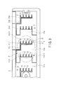
- FIGS. 1 to 5 illustrate a light-emitting device 1.
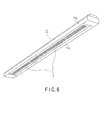
- FIG. 6 illustrates a lighting apparatus 11 including the light-emitting device 1.
- an identical portion is given an identical reference numeral, and a duplicated explanation thereof will be omitted.
- the light-emitting device 1 is provided with a substrate 2, a plurality of light-emitting elements 3, and a phosphor layer 4 covering each of the light-emitting elements 3 as a sealing member.
- FIG. 1 is a partially cutaway plan view of the light-emitting device 1 (the phosphor layer 4 and a resist layer 23 are removed on the right side of the illustration).
- the substrate 2 is made of a material such as a glass epoxy resin and formed in substantially an elongated rectangular shape.
- a length L of the substrate 2 is 250 mm to 300 mm, and a width W thereof is 30 mm to 40 mm. In this embodiment, specifically, the length L is 280 mm, and the width W is 32 mm.
- the thickness of the substrate 2 is preferably 0.5 mm or more and 1.8 mm or less, and is 1 mm in this embodiment.
- Both ends of the substrate 2, for example, in a longer direction may be rounded.
- a ceramics material or other synthetic resin materials as a material for the substrate 2.
- this embodiment does not preclude using a substrate with a metallic base plate to increase heat radiation of each of the light-emitting elements 3.
- a substrate is formed by laminating an insulating layer on a surface of a base plate such as aluminum having high thermal conductivity and good heat radiation performance.
- a wiring pattern 21 and connection patterns 22 are formed on the substrate 2.
- the wiring pattern 21 is formed of mounting pads 21a, power conductors 21b, and power terminals 21c.
- the mounting pads 21a take a large proportion of an area on the substrate 2, and are arranged to take the plurality of light-emitting elements 3 mounted thereon. From the mounting pad 21a, the narrow and bended power conductor 21b continuously extends.
- the power conductor 21b extends in a direction perpendicular to the longer direction of the substrate 2.
- the mounting pads 21a and the power conductors 21b are divided and formed in a plurality of blocks, specifically in 9 blocks, and are provided in the longer direction. Individual adjacent blocks are kept away from each other with an insulation distance to secure the insulating performance.
- power supply posts 21a1 are arranged in a direction perpendicular to the longer direction of the substrate 2.
- the power conductor 21b is provided with power supply posts 21b1.
- five convex power supply posts 21a1 and five convex power supply posts 21b1 are formed at regular intervals, respectively.
- the power terminals 21c are connected to the mounting pads 21a or the power conductors 21b and provided on both sides of the substrate 2. A power connectors are connected to these power terminals 21c.
- connection patterns 22 have a narrow width, are connected to the mounting pads 21a, individually, and extend up to an end edge in a vertical direction of the substrate 2.
- the connection patterns 22 are used when the wiring pattern 21 is subjected to an electrolytic plating process.
- the connection patterns 22 function as a connection path to make a portion of each of the mounting pads 21a equipotential when the wiring pattern 21 is subjected to the electrolytic plating.
- a plating layer is also formed in portions of the connection patterns 22 simultaneously.
- the wiring pattern 21 and the connection patterns 22 have a three-layer structure including a first layer S1, a second layer S2, and a third layer S3.
- first layer S1 copper (Cu) is provided on a surface of the substrate 2.
- second layer S2 nickel (Ni) is processed by electrolytic plating.
- third layer S3 silver (Ag) having a high reflectance is processed by electrolytic plating.
- the third layer S3 of the mounting pads 21a i.e., the surface layer, is formed of silver (Ag) by electrolytic plating and is formed as a reflecting layer whose whole ray reflectance is high as 90%.
- a thickness of nickel (Ni) of the second layer S2 be formed at 5 ⁇ m or more, and a thickness of silver (Ag) of the third layer S3 be at 1 ⁇ m or more.
- a white resist layer 23 having a high reflectance is laminated on almost an entire obverse side of the substrate 2 excluding mounting areas where the light-emitting elements 3 are mounted and mounting portions where components are mounted.
- each of the light-emitting elements 3 is formed of a bare LED chip.
- the bare LED chip that emits blue light is used so that a light-emitting portion is made to emit light of white color.
- the bare LED chip is bonded onto the mounting pad 21a using a silicon resin based insulating adhesive.
- the bare LED chip is an element based on, for example, Indium-Gallium-Nitride series (InGaN) and has a structure in which a light-emitting layer is laminated on a translucent sapphire substrate.
- the light-emitting layer is formed by laminating sequentially an n-type nitride semiconductor layer, an InGaN light-emitting layer, and a p-type nitride semiconductor layer.
- Electrodes for supplying current to the light-emitting layer are formed of a positive electrode that is formed by a p-type electrode pad on the p-type nitride semiconductor layer, and a negative electrode that is formed by an n-type electrode pad on the n-type nitride semiconductor layer.
- Each of the bonding wires 31 is a thin wire made of gold (Au) and is connected through a bump formed of gold (Au) as a principal component to enhance a packaging strength and reduce damage to the bare LED chip.
- the plurality of light-emitting elements 3 are arranged on the mounting pads 21a of the substrate 2 in a manner to form a plurality of rows (light-emitting elements row) in a direction perpendicular to the longer direction of the substrate 2.
- the plurality of light-emitting elements 3 are adhered onto the mounting pad 21a in a manner to individually correspond to the power supply posts 21a1 formed on the mounting pads 21a and the power supply posts 21b1 formed on the power conductors 21b.
- five light-emitting elements 3 are in a light-emitting elements row at substantially a regular intervals, and 18 light-emitting elements rows are formed in a direction perpendicular to the longer direction of the substrate 2 to thereby form an layout pattern of the light-emitting elements 3.
- the plurality of light-emitting elements 3 arranged in a row A in the illustration are connected from a positive pole of the power source to a positive side electrode of the light-emitting element 3 through the power conductor 21b, the power supply post 21b1, and the bonding wire 31, and are connected from a negative side electrode of the light-emitting element 3 to the mounting pad 21a through the bonding wire 31.
- the plurality of light-emitting elements 3 arranged in a row B in the illustration are connected from a positive pole of the power source to a positive side electrode of the light-emitting element 3 through the mounting pad 21a, the power supply posts 21a1, and the bonding wire 31, and are connected from a negative side electrode of the light-emitting element 3 to the mounting pad 21a through the bonding wire 31.
- the light-emitting electrodes 3 are electrically connected in parallel to the power source individually, and the two rows of the rows A and B of the light-emitting elements rows constitute a group P. These connections are repeated sequentially for nine groups of 18 rows in total so that power is supplied to each of the light-emitting elements 3.
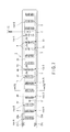
- the light-emitting elements 3 connected as described above form a connection state as illustrated in FIG. 5 .
- nine parallel circuits J each of which includes 10 light-emitting elements 3 connected in parallel form a series circuit K to be connected to the power source.
- an arbitrary number of elements constitutes a group (for example, a group of the row A or a group of the row B) which then constitutes a plurality of groups.
- the light-emitting elements 3 are on the substrate 2 in a divided manner according to each of the groups.
- Each of the parallel circuits J includes the groups, for example.
- Each of the groups includes at least one of (or some of) the light-emitting elements 3.
- the plurality of light-emitting elements 3 in a single parallel circuit J are divided into two rows of light-emitting elements rows (row A and row B) each including five elements and provided on the substrate 2. As a layout pattern, 18 rows of the light-emitting elements rows are included.
- the light-emitting device 1 Even if any one of the light-emitting elements 3 cannot emit light due to a poor connection or a broken wire of the bonding wire 31, the light-emitting device 1 as a whole does not stop emitting light.
- the number of light-emitting elements 3 in the parallel circuit J and the number of the parallel circuits J to be connected in series can be arbitrarily selected according to the design.
- the number of divisions for dividing and laying the plurality of light-emitting elements 3 in a single parallel circuit J i.e., the number of rows of the light-emitting elements rows, can be arbitrarily selected.
- a pair of fitting holes 5 for fitting the substrate is provided between adjacent light-emitting elements rows in a center portion of the substrate 2.
- the fitting holes 5 are used for fitting the light-emitting device 1 to a body or the like of a lighting apparatus.
- a fitting screw 51 serving as a fixing means penetrates through the fitting hole 5 and is screwed into the body or the like of the lighting apparatus so that the light-emitting device 1 is fitted.
- these fitting holes 5 are provided in two end portions of the substrate 2, and therefore it is necessary to secure the space for the holes, which makes the substrate 2 larger by that amount.
- the fixing means is metallic, it is possible to provide an insulating distance.
- the fixing means does not fix the both end portions of the substrate 2 but fixes an inner side in the longer direction, i.e., the middle portion of the substrate 2, it is possible to effectively suppress the deformation of the substrate 2 such as warpage.
- an insulating material such as a synthetic resin as the fixing means.
- the phosphor layer 4 is made of a translucent synthetic resin, e.g., a translucent silicone resin, and contains an appropriate amount of a phosphor such as YAG:Ce (Cerium doped Yttrium-Aluminum-Garnet).
- the phosphor layer 4 is formed of a group of a plurality of convex phosphor layers 4a that respectively cover each of the light-emitting elements 3.
- Each of the convex phosphor layers 4a is formed in a mound-like shape and a circular arc convex shape whose base is formed by being linked with the adjacent convex phosphor layers 4a.
- the phosphor layer 4 is formed along the light-emitting elements rows in a plurality number of rows.
- the phosphor layer 4 is formed in 18 rows and covers and seals each of the light-emitting elements 3 and the bonding wires 31.
- the phosphor is excited by light emitted by the light-emitting element 3 and emits light of a color different from that of the light emitted by the light-emitting element 3.
- the light-emitting element 3 since the light-emitting element 3 emits blue light, a yellow phosphor that emits yellow light which is a complementary color to the blue light is used so that white light can be emitted.
- the phosphor layer 4 is applied, while it is not hardened, in a manner to correspond to each of the light-emitting elements 3 and each of the bonding wires 31 and is hardened thereafter through heat curing or leaving it intact for a predetermined period of time.
- a translucent silicone resin material containing a phosphor whose viscosity and amount are adjusted, while it is not hardened, is supplied from a dispenser (not illustrated) by being dripped in a manner corresponding to each of the light-emitting elements 3 and each of the bonding wires 31.
- each of the light-emitting elements 3 is covered by the convex phosphor layers 4a.
- two or three light-emitting elements 3 may be covered collectively together.
- the substrate 2 is provided with a pattern of copper foil 6 for heat radiation which is formed on an entire surface of a reverse side thereof.
- the heat of the entire substrate 2 is made uniform, which improves the heat radiation performance.
- a resist layer is laminated on the copper foil 6.
- the lighting apparatus 11 in the illustration is a ceiling direct-mounting type lighting apparatus having a size similar to an ordinary lighting apparatus of a 40 W fluorescent type fixed to the ceiling for use.
- the lighting apparatus 11 is provided with a body case 11a having an elongated and substantially rectangular parallelepiped shape.
- the body case 11a includes four of the light-emitting devices 1 that are connected linearly.
- This body case 11a is an example of the "apparatus body”.
- a power supply unit provided with a power circuit is incorporated in the body case 11a.
- a front cover 11b having diffuseness is attached to a lower opening portion of the case 11a.
- the light-emitting elements 3 are lit all together. Light emitted from the light-emitting element 3 passes through the phosphor layer 4 and is radiated. With this arrangement, the light-emitting device 1 is used as a surface light source emitting white light.
- the mounting pad 21a functions as a heat spreader that diffuses heat generated by each of the light-emitting elements 3 while the light-emitting elements 3 emit light.
- the light-emitting device 1 emits light
- light traveling toward the substrate 2 among the light emitted from the light-emitting elements 3 is reflected by the surface layer of the mounting pad 21a mainly to a direction in which the light is utilized. This means that the light-extraction efficiency is made good.
- the light traveling in a side direction among the light emitted from the light-emitting elements 3 is reflected by a surface of the white resist layer 23 having a high reflectance and radiated toward a front side.
- a light-emitting device structured by connecting, in parallel, a plurality of series circuits in which a plurality of LEDs are connected in series is taken.
- the light-emitting elements such as LEDs have individual differences.
- the currents flowing through the individual series circuits in which a plurality of LEDs are connected in series may be different from one another. Consequently, light outputs or emitted colors of the plurality of LEDs of each of the series circuits may differ from one another, which causes a problem in which the uniformity of the illumination light drops as a whole.
- a parallel circuit J is provided with a plurality of light-emitting elements 3 that are connected in parallel, and a plurality of parallel circuits J are connected in series to provide a series circuit K, currents flowing through individual parallel circuits J (a group P in FIG. 3 ) become equal to each another, and thereby variations in light outputs or emitted colors of the individual parallel circuits J are reduced, and the uniformity of the illumination light as a whole can be improved.
- the plurality of light-emitting elements 3 are arranged in a direction perpendicular to the longer direction of the substrate 2 on the mounting pad 21a of the substrate 2 to form light-emitting elements rows. Therefore, it is possible to obtain a desired output by arbitrarily increasing or reducing the number of the light-emitting elements rows.
- FIGS. 7 to 9 a configuration having a function identical with or similar to that of the first embodiment is given the same reference numeral, and an explanation thereof will be omitted.
- configurations other than those described below are the same as those of the first embodiment.
- a first power feed line 25a, a second power feed line 25b, and mounting pads 26 are formed on a substrate 2.
- the first power feed line 25a and the second power feed line 25b are in the form of a wiring pattern and form electric power feed lines independently.
- a positive pole line of the first power feed line 25a is formed linearly in an edge portion in the longer direction of the substrate 2 (upper side in the illustration), and a negative pole line is formed in a comb-like pattern having a plurality of projecting teeth.
- the positive pole line of the second power feed line 25b is formed linearly in an edge portion in the longer direction of the substrate 2 in a similar manner (lower side in the illustration), and a negative pole line is formed in a comb-like pattern having a plurality of projecting teeth that are individually arranged in gaps between adjacent teeth of the first power feed line 25a.
- the projecting teeth of the first power feed line 25a and the projecting teeth of the second power feed line 25b are arranged to be in gaps of each other formed between adjacent teeth of the both lines.
- Power terminals 21c are individually connected to the first power feed lines 25a and the second power feed lines 25b.
- the power terminals 21c are provided at one end portion of the substrate 2 and formed in a manner to be connected to power connectors.
- the plurality of light-emitting elements 3 are arranged on the mounting pads 26 of the substrate 2 in a direction perpendicular to the longer direction of the substrate 2 to form a plurality of rows.
- the light-emitting elements 3 includes light-emitting elements 3a (first light-emitting element) connected to the first power feed line 25a and light-emitting elements 3b (second light-emitting element) connected to the second power feed line 25b.
- six light-emitting elements 3a are at substantially regular intervals between the positive pole line and the negative pole line of the first power feed line 25a.
- six light-emitting elements 3b are at substantially regular intervals between the positive pole line and the negative pole line of the second power feed line 25b.
- the light-emitting elements 3 positioned in the same light-emitting elements row are connected in parallel to the first power feed line 25a or the second power feed line 25b by the bonding wires 31.
- the plurality of light-emitting elements 3 forming each of the light-emitting elements rows are electrically connected to one another in parallel.
- the plurality of light-emitting elements 3a arranged in a row A and the plurality of light-emitting elements 3a arranged in a row B are individually connected in parallel to each another electrically with respect to the first power feed line 25a. This means that two rows formed of rows A and B of the light-emitting element rows constitute a group P in terms of connection.
- the plurality of light-emitting elements 3b arranged in the row A and the plurality of light-emitting elements 3b arranged in the row B are individually connected in parallel to each another electrically with respect to the second power feed ling 25b. This means that two rows formed of the rows A and B of the light-emitting element rows constitute a group P in terms of connection.
- FIG. 9 reflects an actual layout state of the first power feed line 25a, the second power feed line 25b, and the individual light-emitting elements 3 on the substrate 2.
- the parallel circuits J each having 12 light-emitting elements 3a connected in parallel are connected in series to form a series circuit K. Then, among the plurality of light-emitting elements 3a in the parallel circuit J, a plurality of groups each having an arbitrary number of the light-emitting elements 3a (6 in this embodiment) as a group (for example, a group of row A and a group of row B) are formed, and the light-emitting elements 3a are arranged in a divided manner according to each of the groups.
- the parallel circuits J each having 12 light-emitting elements 3b connected in parallel are connected in series to form a series circuit K. Then, among the plurality of light-emitting elements 3b in the parallel circuit J, a plurality of groups each having an arbitrary number of the light-emitting elements 3b (6 in this embodiment) as a group (for example, a group of row A and a group of row B) are formed, and the light-emitting elements 3b are arranged in a divided manner according to each of the groups.
- the light-emitting device 1 even if any one of the light-emitting elements 3 cannot emit light due to a poor connection or a broken wire of the bonding wire 31, the light-emitting device 1 as a whole does not stop emitting light.
- the number of the light-emitting elements 3 in the parallel circuit J and the number of parallel circuits J that are connected in series can be arbitrarily selected according to the design.
- the number of division for dividing the plurality of light-emitting elements 3 in a single parallel circuit J i.e., the number of rows of the light-emitting elements rows, can be arbitrarily selected.
- the first power feed line 25a and the second power feed line 25b form independent electric power feed lines, and therefore the first power feed line 25a and the second power feed line 25b can be selectively switched therebetween by a change-over switch etc. (not illustrated) provided on a power circuit.
- the phosphor layer 4 is made of a translucent synthetic resin, e.g., a translucent silicone resin.
- the phosphor layer 4 includes two types of layers of a first phosphor layer 4Y including a yellow phosphor as a phosphor and a second phosphor layer 4R including a yellow phosphor into which a red phosphor is mixed at a predetermined mixing ratio.
- the first phosphor layer 4Y is an example of a "first sealing member”.
- the second phosphor layer 4R is an example of a "second sealing member”.
- the first phosphor layer 4Y covers the plurality of light-emitting elements 3a connected to the first power feed line 25a.
- the second phosphor layer 4R covers the plurality of light-emitting elements 3b connected to the second power feed line 25b.
- the plurality of light-emitting elements 3a connected to the first feed line 25a and the phosphor layer 4Y constitute a first light source T1.
- the plurality of light-emitting elements 3b connected to the second feed line 25b and the phosphor layer 4R constitute a second light source T2.
- the first light sources T1 and the second light sources T2 form the plurality of rows arranged in the longer direction of the substrate 2 and are disposed alternately in a distributed manner.
- the first light sources T1 connected to the first power feed line 25a that is, individual light-emitting elements 3a connected to the first power feed line 25a, are lit all together.
- the light emitted from the light-emitting element 3a passes through the phosphor layer 4Y and radiated.
- the blue light emitted from the light-emitting element 3a excites the yellow phosphor, is converted into yellow fluorescence by the yellow phosphor, and passes through the phosphor layer 4Y to be radiated outside.
- the light that does not excite the yellow phosphor among the blue light emitted from the light-emitting element 3a passes through the phosphor layer 4Y, as is, and is radiated outside.
- the yellow light and the blue light are combined together to become a daylight color having a correlated color temperature of 7000 K to 5000 K and emitted.
- the correlated color temperature is set at 6700 K.
- the second light sources T2 connected to the second power feed line 25b that is, individual light-emitting elements 3b connected to the second power feed line 25b, are lit all together.
- the light emitted from the light-emitting element 3b passes through the phosphor layer 4R and radiated. In this case, the blue light emitted from the light-emitting element 3b excites the yellow phosphor and at the same time excites the red phosphor.
- the correlated color temperature is set at 2700 K.
- both of the first power feed line 25a and the second power feed line 25b may be energized by the change-over switch etc. on the side of the power circuit.
- all of the light-emitting elements 3 emit light, and both of the first light sources T1 and the second light sources T2 are lit. Therefore, the correlated color temperature becomes the middle of the two.
- the lighting apparatus 11 is provided with a body case 11a having an elongated and substantially rectangular parallelepiped shape, and four of the light-emitting devices 1 are connected linearly and attached to the body case 11a.
- a lot of bare LED chips are mounted on a substrate, and the individual LED chips are electrically connected by bonding wires and sealed with a sealing member containing phosphor. From this arrangement, light in daylight color, white, light bulb color, or the like is obtained.
- a method is conceived to obtain a desired luminance color by laying a plurality of LEDs having different emitting colors such as red, green, or blue on a substrate and mixing colors by adjusting the emission intensities or the like of the individual LEDs.
- This embodiment is made in view of the foregoing subject, and makes it possible to provide a light-emitting device and a lighting apparatus that, with a simple configuration, can change the luminance color and improve the uniformity of illumination light as a whole.
- the light-emitting device 1 it is possible to select a luminance color from among daylight color, white, and light bulb color by means of the first light sources T1 and the second light sources T2.
- the first light sources T1 and the second light sources T2 are arranged in a distributed manner, it is possible to use it as a surface light source that is good in the uniformity in each light emitting color as a whole.
- the number of light-emitting elements 3 and the number of the light-emitting elements rows are same between the first light source T1 and the second light source T2, even if any one of them is selected by switching, the distribution of light does not vary to a larger extent.
- the plurality of light-emitting elements 3 form the light-emitting elements rows by being arranged on the mounting pad 26 of the substrate 2 in a plurality of quantities in a direction perpendicular to the longer direction of the substrate 2, it is possible to obtain a desired output by arbitrarily increasing or decreasing the number of light-emitting elements rows.
- the mounting pad 26 functions as a heat spreader that diffuses heat generated by each of the light-emitting elements 3 while the light-emitting elements 3 emit light.
- the light-emitting device 1 emits light
- light traveling toward the substrate 2 among the light emitted from the light-emitting element 3 is reflected by the surface layer of the mounting pad 26 mainly to a direction in which the light is utilized. This means that the light-extraction efficiency can be made good.
- the light traveling in a side direction among the light emitted from the light-emitting elements 3 is reflected by a surface of the white resist layer 23 having a high reflectance and radiated toward a front side.
- Second to fifth embodiments can provide a light-emitting device and a lighting apparatus that, with a simple configuration, can change the luminance color and improve the uniformity of illumination light as a whole.
- the followings are those light-emitting devices and lighting apparatus.
- FIGS. 10 to 12 a configuration having a function identical with or similar to those of the first and second embodiments is given the same reference numeral, and an explanation thereof will be omitted.
- configurations other than those described below are the same as those of the second embodiment.
- each of light-emitting elements rows different poles of light emitting elements 3 provided adjacent to one another in a direction in which the row extends are sequentially connected by bonding wires 31. That is, a positive pole of one of the adjacent light emitting elements 3 and a negative pole of the other of the adjacent light emitting elements 3 are connected to each other by the bonding wire 31, and this is sequentially repeated.
- the plurality of light-emitting elements 3 constituting individual light-emitting elements rows are electrically connected to one another in series. Accordingly, the plurality of light-emitting elements 3 emit light all together when energized.
- an electrode of one light-emitting element 3 at an end of the row is connected to a first power feed line 25a or a second power feed line 25b by the bonding wire 31.
- FIG. 12 reflects an actual layout state of the first power feed line 25a, the second power feed line 25b, and the individual light-emitting elements 3 on the substrate 2.
- a plurality of rows (9 rows) of the light-emitting elements 3a connected to the first power feed line 25a and a plurality of rows (9 rows) of the light-emitting elements 3b connected to the second power feed line 25b are alternately on the substrate 2 in the longer direction thereof. Accordingly, a total of 18 rows of light-emitting elements rows are provided in a distributed manner.
- Individual light-emitting elements rows are electrically provided in parallel to the first power feed line 25a or the second power feed line 25b and are supplied with power through the first power feed line 25a or the second power feed line 25b. Therefore, even if any one of the light-emitting elements rows can not emit light due to a bonding failure or the like, the light-emitting device 1 as a whole does not stop emitting light.
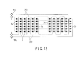
- FIG. 13 a configuration having a function identical with or similar to those of the first and second embodiments is given the same reference numeral, and an explanation thereof will be omitted.
- configurations other than those described below are the same as those of the second embodiment.
- FIG. 13 reflects an actual layout state of a first power feed line 25a, a second power feed line 25b, and individual light-emitting elements 3 on the substrate 2.
- a portion identical with that of the first embodiment is given the same reference numeral, and an explanation thereof will be omitted.
- first power feed line 25a and second power feed line 25b form independent electric power feed lines individually, and therefore the first power feed line 25a and the second power feed line 25b can be selectively switched therebetween by a change-over switch etc. provided on a power circuit.
- FIG. 14 a configuration having a function identical with or similar to those of the first and second embodiments is given the same reference numeral, and an explanation thereof will be omitted.
- configurations other than those described below are the same as those of the second embodiment.
- the first light sources T1 and the second light sources T2 are arranged alternately in a distributed manner in a longer direction of a substrate.
- a phosphor layer 4 has a mound-like shape and covers light-emitting elements 3 individually.
- a lighting apparatus 11 may be provided with the light-emitting device 1 according to any one of the foregoing third to fifth embodiments.
- the embodiments are not limited to the specific configurations of each embodiment described above. Accordingly, various modifications may be made without departing from the spirit or scope of the invention.
- the light-emitting element is a solid-state light-emitting element such as an LED.
- the number of the light-emitting elements to be mounted is not particularly limited.
- the layout pattern of the plurality of light-emitting elements be such a form in which the plurality of light-emitting elements are arranged in a direction perpendicular to the longer direction of the substrate to form a plurality of rows, the embodiment is not particularly limited to this layout pattern.
- the light source is not restricted to two types. To be specific, without limiting to selective switching between the daylight color and the light bulb color, neutral white color, white color, and warm white color are added thereto and are configured in such a way to change the color among these. Furthermore, although white based color is desirable as the light emitting color, the embodiment is not limited to this. For example, it is also possible to selectively change between daylight color and blue color.
- individual color temperature rows may be arbitrarily controlled.
- one of the color temperature groups may be controlled when the light is turned on.
- both of them may be controlled or respectively controlled so that light intensity control or color temperature control may be performed.
- the lighting apparatus can be applied to a lighting apparatus for indoor or outdoor use, or to a display apparatus or the like.
Applications Claiming Priority (2)
| Application Number | Priority Date | Filing Date | Title |
|---|---|---|---|
| JP2010141115A JP2012004517A (ja) | 2010-06-21 | 2010-06-21 | 発光装置及び照明装置 |
| JP2010144326A JP5656051B2 (ja) | 2010-06-24 | 2010-06-24 | 発光装置及び照明装置 |
Publications (2)
| Publication Number | Publication Date |
|---|---|
| EP2397749A2 true EP2397749A2 (de) | 2011-12-21 |
| EP2397749A3 EP2397749A3 (de) | 2015-05-06 |
Family
ID=44652061
Family Applications (1)
| Application Number | Title | Priority Date | Filing Date |
|---|---|---|---|
| EP20110170336 Withdrawn EP2397749A3 (de) | 2010-06-21 | 2011-06-17 | Lichtemittierende Vorrichtung und Beleuchtungsvorrichtung |
Country Status (3)
| Country | Link |
|---|---|
| US (1) | US20110309381A1 (de) |
| EP (1) | EP2397749A3 (de) |
| CN (1) | CN102290408A (de) |
Cited By (5)
| Publication number | Priority date | Publication date | Assignee | Title |
|---|---|---|---|---|
| EP2642835A3 (de) * | 2012-03-23 | 2014-06-11 | Toshiba Lighting & Technology Corporation | Leiterplattenvorrichtung, Lampe und Herstellungsverfahren für Leiterplattenvorrichtung |
| EP2642836A3 (de) * | 2012-03-23 | 2014-06-11 | Toshiba Lighting & Technology Corporation | Leiterplattenvorrichtung, Lampe und Herstellungsverfahren für Leiterplattenvorrichtung |
| EP2878883A4 (de) * | 2012-07-25 | 2015-11-25 | Panasonic Ip Man Co Ltd | Lichtemissionsmodul |
| EP3432692A1 (de) * | 2017-07-18 | 2019-01-23 | ZKW Group GmbH | Thermische kopplung von kupferspreizflächen |
| WO2023031011A1 (en) | 2021-08-30 | 2023-03-09 | Signify Holding B.V. | A lighting device |
Families Citing this family (8)
| Publication number | Priority date | Publication date | Assignee | Title |
|---|---|---|---|---|
| JP2013157592A (ja) * | 2012-01-05 | 2013-08-15 | Canon Components Inc | 発光素子実装用フレキシブル回路基板 |
| US9232634B2 (en) | 2011-01-17 | 2016-01-05 | Canon Components, Inc. | Flexible circuit board for mounting light emitting element, illumination apparatus, and vehicle lighting apparatus |
| CN103629554B (zh) * | 2012-08-21 | 2016-07-06 | 展晶科技(深圳)有限公司 | 照明装置 |
| JP6344689B2 (ja) * | 2013-07-16 | 2018-06-20 | パナソニックIpマネジメント株式会社 | 基板、発光装置、照明用光源、および照明装置 |
| US10622517B2 (en) * | 2016-08-16 | 2020-04-14 | Sharp Kabushiki Kaisha | Lighting device and display device |
| US9902314B1 (en) * | 2016-11-17 | 2018-02-27 | Ford Global Technologies, Llc | Vehicle light system |
| FR3061625B1 (fr) * | 2016-12-30 | 2020-07-24 | Commissariat Energie Atomique | Structure electronique comprenant une matrice de dispositifs electroniques presentant des performances thermiques ameliorees |
| CN108336081B (zh) * | 2018-04-03 | 2019-12-31 | 广东雷腾智能光电有限公司 | 一种cob光源及cob基板 |
Family Cites Families (10)
| Publication number | Priority date | Publication date | Assignee | Title |
|---|---|---|---|---|
| JPH06140451A (ja) * | 1992-10-27 | 1994-05-20 | Hitachi Ltd | 半導体集積回路装置 |
| WO2003016782A1 (en) * | 2001-08-09 | 2003-02-27 | Matsushita Electric Industrial Co., Ltd. | Led illuminator and card type led illuminating light source |
| KR100875443B1 (ko) * | 2006-03-31 | 2008-12-23 | 서울반도체 주식회사 | 발광 장치 |
| CN101416323B (zh) * | 2006-04-10 | 2011-03-30 | 夏普株式会社 | Led组件和包括该led组件的照明装置和液晶显示装置 |
| JP2008218485A (ja) * | 2007-02-28 | 2008-09-18 | Toshiba Lighting & Technology Corp | 発光装置 |
| US20090050912A1 (en) * | 2007-08-24 | 2009-02-26 | Foxsemicon Integrated Technology, Inc. | Light emitting diode and outdoor illumination device having the same |
| CN201177226Y (zh) * | 2008-03-24 | 2009-01-07 | 东莞勤上光电股份有限公司 | Led灯板 |
| JP5380451B2 (ja) * | 2008-08-11 | 2014-01-08 | ローム株式会社 | 照明装置 |
| CN101771025A (zh) * | 2008-12-26 | 2010-07-07 | 富准精密工业(深圳)有限公司 | 发光二极管 |
| KR20100043168A (ko) * | 2010-04-09 | 2010-04-28 | 엔엘티테크주식회사 | 백색광 엘이디를 이용한 조명기구 |
-
2011
- 2011-06-16 US US13/162,150 patent/US20110309381A1/en not_active Abandoned
- 2011-06-17 EP EP20110170336 patent/EP2397749A3/de not_active Withdrawn
- 2011-06-17 CN CN2011101643334A patent/CN102290408A/zh active Pending
Non-Patent Citations (1)
| Title |
|---|
| None |
Cited By (6)
| Publication number | Priority date | Publication date | Assignee | Title |
|---|---|---|---|---|
| EP2642835A3 (de) * | 2012-03-23 | 2014-06-11 | Toshiba Lighting & Technology Corporation | Leiterplattenvorrichtung, Lampe und Herstellungsverfahren für Leiterplattenvorrichtung |
| EP2642836A3 (de) * | 2012-03-23 | 2014-06-11 | Toshiba Lighting & Technology Corporation | Leiterplattenvorrichtung, Lampe und Herstellungsverfahren für Leiterplattenvorrichtung |
| EP2878883A4 (de) * | 2012-07-25 | 2015-11-25 | Panasonic Ip Man Co Ltd | Lichtemissionsmodul |
| US9416924B2 (en) | 2012-07-25 | 2016-08-16 | Panasonic Intellectual Property Management Co., Ltd. | Light emission module |
| EP3432692A1 (de) * | 2017-07-18 | 2019-01-23 | ZKW Group GmbH | Thermische kopplung von kupferspreizflächen |
| WO2023031011A1 (en) | 2021-08-30 | 2023-03-09 | Signify Holding B.V. | A lighting device |
Also Published As
| Publication number | Publication date |
|---|---|
| EP2397749A3 (de) | 2015-05-06 |
| US20110309381A1 (en) | 2011-12-22 |
| CN102290408A (zh) | 2011-12-21 |
Similar Documents
| Publication | Publication Date | Title |
|---|---|---|
| EP2397749A2 (de) | Lichtemittierende Vorrichtung und Beleuchtungsvorrichtung | |
| US8872198B2 (en) | Luminaire and light-emitting apparatus with light-emitting device | |
| JP5197874B2 (ja) | 発光モジュール、光源装置、液晶表示装置および発光モジュールの製造方法 | |
| US9488345B2 (en) | Light emitting device, illumination apparatus including the same, and mounting substrate | |
| US8847251B2 (en) | Substrate, light-emitting device, and lighting apparatus having a largest gap between two lines at light-emitting element mounting position | |
| US20110309379A1 (en) | Light-emitting device and luminare | |
| JP6440060B2 (ja) | 発光装置、及びそれを用いた照明装置 | |
| US20100258819A1 (en) | Substrate for an led submount, and led submount | |
| WO2011129203A1 (ja) | 発光装置 | |
| US8766536B2 (en) | Light-emitting module having light-emitting elements sealed with sealing member and luminaire having same | |
| JP5408414B2 (ja) | 発光モジュール | |
| EP2672513B1 (de) | Mehrchip-Verpackungsstruktur zum Erzeugen einer symmetrischen und gleichmäßigen Mischlichtquelle | |
| JP6083253B2 (ja) | 発光装置の積層体 | |
| JP2011192703A (ja) | 発光装置及び照明装置 | |
| US10490721B2 (en) | Light-emitting device and illuminating apparatus | |
| US20150173137A1 (en) | Light-emitting device | |
| JP6941923B2 (ja) | Ledモジュールの製造方法及びledモジュール | |
| JP2010251796A (ja) | 発光モジュール | |
| JP5656051B2 (ja) | 発光装置及び照明装置 | |
| JP5769129B2 (ja) | 発光装置及び照明装置 | |
| JP2009212126A (ja) | 照明装置 | |
| JP5212178B2 (ja) | 発光モジュール | |
| JP2011090972A (ja) | 発光装置及び照明装置 |
Legal Events
| Date | Code | Title | Description |
|---|---|---|---|
| 17P | Request for examination filed |
Effective date: 20110617 |
|
| AK | Designated contracting states |
Kind code of ref document: A2 Designated state(s): AL AT BE BG CH CY CZ DE DK EE ES FI FR GB GR HR HU IE IS IT LI LT LU LV MC MK MT NL NO PL PT RO RS SE SI SK SM TR |
|
| AX | Request for extension of the european patent |
Extension state: BA ME |
|
| PUAI | Public reference made under article 153(3) epc to a published international application that has entered the european phase |
Free format text: ORIGINAL CODE: 0009012 |
|
| PUAL | Search report despatched |
Free format text: ORIGINAL CODE: 0009013 |
|
| AK | Designated contracting states |
Kind code of ref document: A3 Designated state(s): AL AT BE BG CH CY CZ DE DK EE ES FI FR GB GR HR HU IE IS IT LI LT LU LV MC MK MT NL NO PL PT RO RS SE SI SK SM TR |
|
| AX | Request for extension of the european patent |
Extension state: BA ME |
|
| RIC1 | Information provided on ipc code assigned before grant |
Ipc: F21Y 105/00 20060101ALN20150405BHEP Ipc: F21Y 101/02 20060101ALN20150405BHEP Ipc: F21S 8/04 20060101AFI20150405BHEP Ipc: H01L 33/50 20100101ALN20150405BHEP Ipc: H05K 1/18 20060101ALN20150405BHEP Ipc: H01L 25/075 20060101ALI20150405BHEP Ipc: H05K 1/02 20060101ALI20150405BHEP |
|
| STAA | Information on the status of an ep patent application or granted ep patent |
Free format text: STATUS: THE APPLICATION HAS BEEN WITHDRAWN |
|
| 18W | Application withdrawn |
Effective date: 20150525 |