EP2395547A2 - Substrat mit gesinterter Unterplatte - Google Patents
Substrat mit gesinterter Unterplatte Download PDFInfo
- Publication number
- EP2395547A2 EP2395547A2 EP11163824A EP11163824A EP2395547A2 EP 2395547 A2 EP2395547 A2 EP 2395547A2 EP 11163824 A EP11163824 A EP 11163824A EP 11163824 A EP11163824 A EP 11163824A EP 2395547 A2 EP2395547 A2 EP 2395547A2
- Authority
- EP
- European Patent Office
- Prior art keywords
- metallic layer
- metal
- package
- electronic device
- recited
- Prior art date
- Legal status (The legal status is an assumption and is not a legal conclusion. Google has not performed a legal analysis and makes no representation as to the accuracy of the status listed.)
- Withdrawn
Links
Images
Classifications
-
- B—PERFORMING OPERATIONS; TRANSPORTING
- B23—MACHINE TOOLS; METAL-WORKING NOT OTHERWISE PROVIDED FOR
- B23K—SOLDERING OR UNSOLDERING; WELDING; CLADDING OR PLATING BY SOLDERING OR WELDING; CUTTING BY APPLYING HEAT LOCALLY, e.g. FLAME CUTTING; WORKING BY LASER BEAM
- B23K1/00—Soldering, e.g. brazing, or unsoldering
- B23K1/0008—Soldering, e.g. brazing, or unsoldering specially adapted for particular articles or work
- B23K1/0016—Brazing of electronic components
-
- B—PERFORMING OPERATIONS; TRANSPORTING
- B22—CASTING; POWDER METALLURGY
- B22F—WORKING METALLIC POWDER; MANUFACTURE OF ARTICLES FROM METALLIC POWDER; MAKING METALLIC POWDER; APPARATUS OR DEVICES SPECIALLY ADAPTED FOR METALLIC POWDER
- B22F7/00—Manufacture of composite layers, workpieces, or articles, comprising metallic powder, by sintering the powder, with or without compacting wherein at least one part is obtained by sintering or compression
- B22F7/02—Manufacture of composite layers, workpieces, or articles, comprising metallic powder, by sintering the powder, with or without compacting wherein at least one part is obtained by sintering or compression of composite layers
- B22F7/04—Manufacture of composite layers, workpieces, or articles, comprising metallic powder, by sintering the powder, with or without compacting wherein at least one part is obtained by sintering or compression of composite layers with one or more layers not made from powder, e.g. made from solid metal
-
- B—PERFORMING OPERATIONS; TRANSPORTING
- B32—LAYERED PRODUCTS
- B32B—LAYERED PRODUCTS, i.e. PRODUCTS BUILT-UP OF STRATA OF FLAT OR NON-FLAT, e.g. CELLULAR OR HONEYCOMB, FORM
- B32B15/00—Layered products comprising a layer of metal
- B32B15/01—Layered products comprising a layer of metal all layers being exclusively metallic
- B32B15/017—Layered products comprising a layer of metal all layers being exclusively metallic one layer being formed of aluminium or an aluminium alloy, another layer being formed of an alloy based on a non ferrous metal other than aluminium
-
- B—PERFORMING OPERATIONS; TRANSPORTING
- B23—MACHINE TOOLS; METAL-WORKING NOT OTHERWISE PROVIDED FOR
- B23K—SOLDERING OR UNSOLDERING; WELDING; CLADDING OR PLATING BY SOLDERING OR WELDING; CUTTING BY APPLYING HEAT LOCALLY, e.g. FLAME CUTTING; WORKING BY LASER BEAM
- B23K2101/00—Articles made by soldering, welding or cutting
- B23K2101/36—Electric or electronic devices
-
- H10W72/07331—
-
- H10W72/07336—
-
- H10W72/352—
-
- H10W72/59—
-
- H10W72/923—
-
- H10W72/952—
-
- Y—GENERAL TAGGING OF NEW TECHNOLOGICAL DEVELOPMENTS; GENERAL TAGGING OF CROSS-SECTIONAL TECHNOLOGIES SPANNING OVER SEVERAL SECTIONS OF THE IPC; TECHNICAL SUBJECTS COVERED BY FORMER USPC CROSS-REFERENCE ART COLLECTIONS [XRACs] AND DIGESTS
- Y02—TECHNOLOGIES OR APPLICATIONS FOR MITIGATION OR ADAPTATION AGAINST CLIMATE CHANGE
- Y02P—CLIMATE CHANGE MITIGATION TECHNOLOGIES IN THE PRODUCTION OR PROCESSING OF GOODS
- Y02P10/00—Technologies related to metal processing
- Y02P10/25—Process efficiency
-
- Y—GENERAL TAGGING OF NEW TECHNOLOGICAL DEVELOPMENTS; GENERAL TAGGING OF CROSS-SECTIONAL TECHNOLOGIES SPANNING OVER SEVERAL SECTIONS OF THE IPC; TECHNICAL SUBJECTS COVERED BY FORMER USPC CROSS-REFERENCE ART COLLECTIONS [XRACs] AND DIGESTS
- Y10—TECHNICAL SUBJECTS COVERED BY FORMER USPC
- Y10T—TECHNICAL SUBJECTS COVERED BY FORMER US CLASSIFICATION
- Y10T428/00—Stock material or miscellaneous articles
- Y10T428/12—All metal or with adjacent metals
- Y10T428/12007—Component of composite having metal continuous phase interengaged with nonmetal continuous phase
-
- Y—GENERAL TAGGING OF NEW TECHNOLOGICAL DEVELOPMENTS; GENERAL TAGGING OF CROSS-SECTIONAL TECHNOLOGIES SPANNING OVER SEVERAL SECTIONS OF THE IPC; TECHNICAL SUBJECTS COVERED BY FORMER USPC CROSS-REFERENCE ART COLLECTIONS [XRACs] AND DIGESTS
- Y10—TECHNICAL SUBJECTS COVERED BY FORMER USPC
- Y10T—TECHNICAL SUBJECTS COVERED BY FORMER US CLASSIFICATION
- Y10T428/00—Stock material or miscellaneous articles
- Y10T428/12—All metal or with adjacent metals
- Y10T428/12493—Composite; i.e., plural, adjacent, spatially distinct metal components [e.g., layers, joint, etc.]
- Y10T428/12736—Al-base component
- Y10T428/1275—Next to Group VIII or IB metal-base component
Definitions
- This disclosure relates to bonded structures having a robust interface that can withstand elevated temperature processing conditions without delamination.
- a bonded structure such as a silicon die that is bonded to a substrate, typically includes multiple layers of metals that bond the die and the substrate together and provide thermal transfer between the die and package. Manufacturers of such bonded structures typically fabricate the structure at processing temperatures that do not exceed 300°C.
- the present invention provides a substrate comprising: a metal portion; and an underplate that is laser sintered to the metal portion, wherein the metal portion has a melting point that is lower than a sintering temperature of the underplate.
- the metal portion may be aluminum and the underplate may be nickel metal.
- the metal portion may be a metal matrix of a composite which may comprise silicon carbide.
- the metal portion may be an electronic device package and the underplate be a metallic layer on the electronic device package.
- the invention provides an electronic device comprising: an electronic device package having a metallic layer thereon such that there is a metallic layer/package interface, and the metallic layer/package interface is laser sintered.
- the electronic device may further comprise a silicon-containing die and a bonding material on the metallic layer which bonds the electronic device package and the silicon-containing die together, wherein the electronic device package is an aluminum silicon carbide (AlSiC) package.
- the silicon-containing die may include a titanium metal layer and a nickel metal layer.
- the metallic layer may be selected from a group consisting of nickel metal and copper metal, for example nickel metal.
- the metallic layer/package interface may be such as not to crack or blister at a processing temperature greater than 350°C.
- the electronic device package may be a metal matrix composite having silicon carbide reinforcement dispersed in an aluminum metal matrix.
- the metallic layer may be laser-applied.
- the invention provides an electronic device comprising: a silicon-containing die; an aluminum silicon carbide (AlSiC) package including a nickel metal layer thereon having a sintered interface with the AlSiC package; and a bonding material that bonds the nickel metal layer on the AlSiC package and the silicon-containing die together.
- AlSiC aluminum silicon carbide
- the invention provides a bonded structure comprising: a structural member including aluminum metal; a metallic layer on the structural member, the metallic layer having a sintered interface with the structural member, and the metallic layer is selected from a group consisting of nickel metal and copper metal; and a bonding material on the metallic layer operable to bond the structural member and another component together.
- the metallic layer may be the nickel metal.
- the bonding material may comprise gold and tin.
- the invention provides a method for processing an electronic device, the method comprising: depositing a metallic layer on an aluminum silicon carbide (AlSiC) package using an energy beam such that there is a metallic layer/AlSiC interface that is laser sintered; depositing a bonding material between the metallic layer and a silicon-containing die; and heating the bonding material to fuse the silicon-containing die and the AlSiC package together without delamination of the metallic layer/AlSiC interface.
- AlSiC aluminum silicon carbide
- the heating of the bonding material may be conducted at a temperature greater than 350°C.
- the metallic layer may be selected from a group consisting of nickel metal and copper metal, for example nickel metal.
- the energy beam may be a laser or an electron beam.
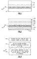
- FIG. 1 illustrates an example bonded structure 20, which is not limited to any particular kind or application.
- the bonded structure 20 includes a structural member 22 having a metal portion, such as aluminum metal in a metal matrix composite.
- An underplate, metallic layer 24, is located on the structural member 22.
- the metallic layer 24 is between the structural member 22 and another component 26 to which the structural member 22 is bonded via bonding material 28. That is, the metallic layer 24 is an underplate with regard to the bonding material 28.
- the bonding material 28 is not limited to any particular kind but may be a solder material, a diffusion bonding material (e.g., gold and tin) or other suitable material for attaching the structural member 22 and the component 26 together.
- the structural member 22 and metallic layer 24 may be provided as a substrate for subsequent processing to attach the component 26.
- the metallic layer 24 is located directly on the structural member 22 and has a sintered interface 30 that serves to facilitate formation of a robust interface between the structural member 22 and the component 26 that can withstand subsequent processing temperatures that are greater than 350°C without delamination.
- the metallic layer 24 may be nickel metal, copper metal, or other suitable metal for the particular application of the bonded structure 20.
- the selected metal may serve as a thermal conductor between the structural member 22 and the component 26, facilitate bonding between the structural member 22 and the component 26, and/or serve another desired purpose within the bonded structure 20. In any case, continuous contact between the metallic layer 24 and the structural member 22 facilitates efficient thermal conductivity and good bond strength.
- the sintered interface 30 forms during processing of the bonded structure 20.
- the metallic layer 24 is deposited onto the structural member 22 using a high energy beam.
- the high energy beam may be a laser or an electron beam that is directed toward a target source of metal that is selected for the metallic layer 24.
- the high energy beam irradiates the target source material, which heats and evaporates or sublimes, to form a high energy plume of the metal that deposits onto the surface of the structural member 22 to form the sintered interface 30.
- the process of applying heat and depositing the source material in a high energy plume causes thermal consolidation of the material to form the sintered interface 30 of the metallic layer 24. Additionally, the use of the high energy beam and target source material does not subject the structural member 22 to the high processing temperatures required to form the high energy plume.
- the material that is deposited as the metallic layer 24 can have a sintering temperature that is higher than the melting temperature of the metal of the structural member 22.
- aluminum in the structural member has a melting point of approximately 1221°F (660°C) while the temperature that the target source material heats up to in order to deposit the metallic layer 24, such as nickel, is much greater. Sintering the metallic layer 24 in situ would otherwise melt the metal portion of the structural member 22.
- the sintered interface 30 may be regarded to be the microstructure of the metallic layer 24 and surface region of the structural member 22 that is formed by using the above discussed deposition process, the mechanical interface between the metallic layer 24 and the structural member 22, or another physical characteristic of the sintered interface 30 that is associated with deposition of the metallic layer 24 using a high energy beam. That is, the sintered interface 30 is a physical characteristic of laser-application of the metallic layer 24.
- the sintered interface 30 of the bonded structure 20 is robust and can withstand downstream processing temperatures of 350°C or greater.
- the sintered interface 30 limits or avoids blistering, cracking, and delamination due to thermal stress from such processing temperatures that might otherwise damage the metallic layer 24 if it were deposited using other methods, such as flame spray and the like.
- the metallic layer 24 is therefore in continuous contact with the structural member 22 even after a heat history of 350°C or greater.
- Figure 2 illustrates another bonded structure, which in this example, is an electronic device 120.
- the electronic device 120 includes an AlSiC package 122 and a metallic layer 124 located on the AlSiC package 122.
- the metallic layer 124 may have a thickness of approximately 1-6 micrometers, however, a user may select another desirable thickness to meet the needs of a particular application.
- the AlSiC package 122 may be a metal matrix composite having silicon carbide reinforcement 122a dispersed in an aluminum metal matrix 122b.
- the AlSiC package 122 is bonded to a silicon-containing die 126, such as a silicon die or a silicon carbide die, by way of a bonding material 128.
- the silicon-containing die 126 optionally includes layers 126a and 126b.
- the layers 126a and 126b may be, respectively, titanium metal and nickel metal for facilitating bonding and thermal conductivity between the AlSiC package 122 and the silicon-containing die 126. It is to be understood that the layers 126a and 126b may alternatively be other types of metal layers, depending upon the particular needs of an application.
- the metallic layer 124 may be nickel metal, copper metal, or other suitable metal for the particular application.
- the electronic device 120 includes a sintered interface 130 between the metallic layer 124 and the AlSiC package 122.
- the sintered interface 130 is a physical characteristic of the high energy beam deposition process that is used to deposit the metallic layer 124 onto the AlSiC package 122.
- the sintered interface 130 is robust and permits downstream high temperature processing of the electronic device 120 without blistering, cracking, or delamination.
- the bonding material 128 may be processed at temperatures of 350°C or grater to fuse the AlSiC package 122 and silicon-containing die 126 together.
- the sintered interface 130 of the electronic device 120 permits processing at such temperatures without delamination such that the metallic layer 124 and the AlSiC package 122 remain in continuous contact across the interface after a heat history of 350°C or greater. This facilitates good thermal conductivity between the metallic layer 124 and the AlSiC package 122 such that the die junction temperature can remain low during operation.
- the sintered interface 130 between the metallic layer 124 and the AlSiC package 122 is approximately an order of magnitude more robust with regard to thermal fatigue than a similar metallic layer that is deposited using other techniques, such as flame spray deposition.
- Figure 3 illustrates an example method 160 for processing an electronic device, such as the electronic device 120 of Figure 2 .
- the method includes a deposition step 162 for depositing the metallic layer 124, a deposition step 164 for depositing the bonding material 128, and a heating step 166 for fusing the silicon-containing die 126 and AlSiC package 122 together without delamination of the interface 130.
- the metallic layer 124 is deposited onto the AlSiC package 122 using a high energy beam, such as a laser or electron beam.
- the bonding material 128 is deposited between the silicon-containing die 126 and the AlSiC package 122.
- the bonding material 128 may be deposited onto the silicon-containing die 126, the AlSiC package 122, or both.
- the bonding material 128 may include one or more layers of metallic materials that are later heated to form a bond.
- the electronic device is heated at the heating step 166 to form the bond between the silicon-containing die 126 and the AlSiC package 122.
- the heating temperature may be 350°C or greater and does not cause delamination of the sintered interface 130, as described above. That is, the sintered interface 130 is strong enough to withstand the thermal stresses from the elevated processing temperatures.
Landscapes
- Engineering & Computer Science (AREA)
- Mechanical Engineering (AREA)
- Chemical & Material Sciences (AREA)
- Composite Materials (AREA)
- Manufacturing & Machinery (AREA)
- Materials Engineering (AREA)
- Die Bonding (AREA)
- Powder Metallurgy (AREA)
- Cooling Or The Like Of Semiconductors Or Solid State Devices (AREA)
- Computer Hardware Design (AREA)
- Microelectronics & Electronic Packaging (AREA)
- Power Engineering (AREA)
Applications Claiming Priority (2)
| Application Number | Priority Date | Filing Date | Title |
|---|---|---|---|
| US32904710P | 2010-04-28 | 2010-04-28 | |
| US12/913,839 US9346114B2 (en) | 2010-04-28 | 2010-10-28 | Substrate having laser sintered underplate |
Publications (1)
| Publication Number | Publication Date |
|---|---|
| EP2395547A2 true EP2395547A2 (de) | 2011-12-14 |
Family
ID=44774263
Family Applications (1)
| Application Number | Title | Priority Date | Filing Date |
|---|---|---|---|
| EP11163824A Withdrawn EP2395547A2 (de) | 2010-04-28 | 2011-04-27 | Substrat mit gesinterter Unterplatte |
Country Status (4)
| Country | Link |
|---|---|
| US (1) | US9346114B2 (de) |
| EP (1) | EP2395547A2 (de) |
| JP (1) | JP2011233890A (de) |
| CN (1) | CN102267260A (de) |
Families Citing this family (2)
| Publication number | Priority date | Publication date | Assignee | Title |
|---|---|---|---|---|
| CN103515521B (zh) * | 2013-09-16 | 2016-06-08 | 惠州雷士光电科技有限公司 | 一种覆铜AlSiC复合散热基板及其制备方法 |
| US20250387845A1 (en) * | 2024-06-25 | 2025-12-25 | The Boeing Company | Systems and methods for joining metal matrix composite materials |
Family Cites Families (29)
| Publication number | Priority date | Publication date | Assignee | Title |
|---|---|---|---|---|
| JPS55117584A (en) * | 1979-03-05 | 1980-09-09 | Hitachi Ltd | Surface alloying method by laser light |
| JPS5865592A (ja) * | 1981-10-16 | 1983-04-19 | Toshiba Corp | レ−ザ溶接方法 |
| JPS61270376A (ja) * | 1985-01-22 | 1986-11-29 | Toyota Motor Corp | 耐摩耗性Al合金部材 |
| US4826736A (en) * | 1985-06-14 | 1989-05-02 | Sumitomo Special Metals Co., Ltd. | Clad sheets |
| JPS62253762A (ja) | 1986-04-25 | 1987-11-05 | Mitsubishi Heavy Ind Ltd | Zn合金の蒸着方法 |
| EP0538244B1 (de) | 1986-10-17 | 1996-05-22 | Board Of Regents, The University Of Texas System | Verfahren und Vorrichtung zur Herstellung von gesinterten Formkörpern durch Teilsinterung |
| JP2769338B2 (ja) * | 1988-11-30 | 1998-06-25 | 昭和アルミニウム株式会社 | 耐摩耗性に優れたアルミニウム合金材の製造方法 |
| US5156697A (en) | 1989-09-05 | 1992-10-20 | Board Of Regents, The University Of Texas System | Selective laser sintering of parts by compound formation of precursor powders |
| JPH045266A (ja) | 1990-04-24 | 1992-01-09 | Toyo Pharma- Kk | ドパミン誘導体の製造方法 |
| JP2890686B2 (ja) * | 1990-06-12 | 1999-05-17 | 松下電器産業株式会社 | レーザ・スパッタリング装置 |
| JPH07102386A (ja) | 1993-10-01 | 1995-04-18 | Mazda Motor Corp | アルミニウム合金部材の表面硬化方法 |
| JP2000007456A (ja) | 1998-06-25 | 2000-01-11 | Toyota Motor Corp | 高熱伝導性セラミックス金属複合材料 |
| US20020063117A1 (en) * | 2000-04-19 | 2002-05-30 | Church Kenneth H. | Laser sintering of materials and a thermal barrier for protecting a substrate |
| MXPA03010716A (es) | 2001-05-24 | 2004-05-27 | Fry Metals Inc | Material de interfaz termico y configuracion disparadora de calor. |
| US20050136640A1 (en) * | 2002-01-07 | 2005-06-23 | Chuan Hu | Die exhibiting an effective coefficient of thermal expansion equivalent to a substrate mounted thereon, and processes of making same |
| US20040151935A1 (en) | 2003-02-03 | 2004-08-05 | Robert Dzugan | Co-continuous metal-ceramic article and method for manufacture thereof |
| WO2004075211A1 (en) | 2003-02-20 | 2004-09-02 | The Regents Of The University Of California | Method of forming conductors at low temperatures using metallic nanocrystals and product |
| US20050191200A1 (en) | 2004-02-27 | 2005-09-01 | Guido Canzona | Method and composition for metal free form fabrication |
| TWI290126B (en) | 2004-08-18 | 2007-11-21 | Delta Electronics Inc | The method of die forming |
| CA2584851C (en) | 2004-11-04 | 2015-04-07 | Microchips, Inc. | Compression and cold weld sealing methods and devices |
| US7645337B2 (en) * | 2004-11-18 | 2010-01-12 | The Trustees Of Columbia University In The City Of New York | Systems and methods for creating crystallographic-orientation controlled poly-silicon films |
| TWI514522B (zh) | 2005-03-18 | 2015-12-21 | 同和電子科技有限公司 | 副載置片及其製造方法 |
| CN100439521C (zh) * | 2005-04-19 | 2008-12-03 | 沈阳大陆激光技术有限公司 | 一种移动式激光熔覆现场加工的合金粉末材料 |
| CN101228295A (zh) | 2005-06-20 | 2008-07-23 | 普莱克斯S.T.技术有限公司 | 在低耐热基底上的激光镀覆 |
| JP5273922B2 (ja) * | 2006-12-28 | 2013-08-28 | 株式会社アライドマテリアル | 放熱部材および半導体装置 |
| US20090020876A1 (en) | 2007-07-20 | 2009-01-22 | Hertel Thomas A | High temperature packaging for semiconductor devices |
| JP2009038162A (ja) | 2007-08-01 | 2009-02-19 | Sumitomo Electric Ind Ltd | 放熱部品、その製造方法及びパワーモジュール |
| KR101480551B1 (ko) * | 2008-04-04 | 2015-01-08 | 엘지이노텍 주식회사 | 수직구조 그룹 3족 질화물계 반도체 발광다이오드 소자 및이의 제조 방법 |
| US8067305B2 (en) | 2008-09-03 | 2011-11-29 | Ultratech, Inc. | Electrically conductive structure on a semiconductor substrate formed from printing |
-
2010
- 2010-10-28 US US12/913,839 patent/US9346114B2/en active Active
-
2011
- 2011-04-22 JP JP2011095592A patent/JP2011233890A/ja active Pending
- 2011-04-27 EP EP11163824A patent/EP2395547A2/de not_active Withdrawn
- 2011-04-28 CN CN2011101085465A patent/CN102267260A/zh active Pending
Non-Patent Citations (1)
| Title |
|---|
| None |
Also Published As
| Publication number | Publication date |
|---|---|
| JP2011233890A (ja) | 2011-11-17 |
| US20110268982A1 (en) | 2011-11-03 |
| US9346114B2 (en) | 2016-05-24 |
| CN102267260A (zh) | 2011-12-07 |
Similar Documents
| Publication | Publication Date | Title |
|---|---|---|
| JP5548167B2 (ja) | 積層体及び積層体の製造方法 | |
| TW200900242A (en) | Reactive multilayer joining with improved metallization techniques | |
| CN107787259B (zh) | 用于制造复合材料的方法 | |
| CN107408538A (zh) | 电路基板及半导体装置 | |
| US9905532B2 (en) | Methods and apparatuses for high temperature bonding and bonded substrates having variable porosity distribution formed therefrom | |
| US9620434B1 (en) | High temperature bonding processes incorporating metal particles and bonded substrates formed therefrom | |
| JP5991103B2 (ja) | ヒートシンク付パワーモジュール用基板、ヒートシンク付パワーモジュール、及びヒートシンク付パワーモジュール用基板の製造方法 | |
| TW201246386A (en) | Metallic thermal joint for high power density chips | |
| RU2696910C2 (ru) | Распыляемая мишень | |
| EP2395547A2 (de) | Substrat mit gesinterter Unterplatte | |
| JP6939973B2 (ja) | 銅/セラミックス接合体、及び、絶縁回路基板 | |
| JP5733466B2 (ja) | 半導体装置の製造方法 | |
| CN101996954B (zh) | 芯片 | |
| WO2020065700A1 (ja) | 金属接合体および金属接合体の製造方法、並びに半導体装置および導波路 | |
| JP6260941B2 (ja) | 半導体装置の製造方法 | |
| EP2048710A1 (de) | Hochtemperaturverpackung für Halbleitervorrichtungen | |
| KR102735500B1 (ko) | 모든 알루미늄 히터 | |
| JP6344605B2 (ja) | 半導体装置の製造方法 | |
| JP5974152B2 (ja) | セラミックス部材と金属部材との接合体及びその製法 | |
| JP2014063798A (ja) | セラミックス回路基板 |
Legal Events
| Date | Code | Title | Description |
|---|---|---|---|
| AK | Designated contracting states |
Kind code of ref document: A2 Designated state(s): AL AT BE BG CH CY CZ DE DK EE ES FI FR GB GR HR HU IE IS IT LI LT LU LV MC MK MT NL NO PL PT RO RS SE SI SK SM TR |
|
| AX | Request for extension of the european patent |
Extension state: BA ME |
|
| PUAI | Public reference made under article 153(3) epc to a published international application that has entered the european phase |
Free format text: ORIGINAL CODE: 0009012 |
|
| STAA | Information on the status of an ep patent application or granted ep patent |
Free format text: STATUS: THE APPLICATION HAS BEEN WITHDRAWN |
|
| 18W | Application withdrawn |
Effective date: 20140224 |