EP2383771A1 - Dispositif et procédé d'enlèvement d'une couche polymère de la surface d'un substrat - Google Patents
Dispositif et procédé d'enlèvement d'une couche polymère de la surface d'un substrat Download PDFInfo
- Publication number
- EP2383771A1 EP2383771A1 EP10004509A EP10004509A EP2383771A1 EP 2383771 A1 EP2383771 A1 EP 2383771A1 EP 10004509 A EP10004509 A EP 10004509A EP 10004509 A EP10004509 A EP 10004509A EP 2383771 A1 EP2383771 A1 EP 2383771A1
- Authority
- EP
- European Patent Office
- Prior art keywords
- substrate
- polymer layer
- fluid
- heating
- diameter
- Prior art date
- Legal status (The legal status is an assumption and is not a legal conclusion. Google has not performed a legal analysis and makes no representation as to the accuracy of the status listed.)
- Granted
Links
- 229920000642 polymer Polymers 0.000 title claims abstract description 70
- 239000000758 substrate Substances 0.000 title claims abstract description 59
- 238000000034 method Methods 0.000 title claims abstract description 12
- 239000011248 coating agent Substances 0.000 title 1
- 238000000576 coating method Methods 0.000 title 1
- 238000010438 heat treatment Methods 0.000 claims abstract description 59
- 239000012530 fluid Substances 0.000 claims abstract description 57
- 239000000126 substance Substances 0.000 claims description 10
- 239000000203 mixture Substances 0.000 claims description 4
- 238000004140 cleaning Methods 0.000 description 7
- 229920002120 photoresistant polymer Polymers 0.000 description 5
- 239000007788 liquid Substances 0.000 description 4
- 238000009826 distribution Methods 0.000 description 3
- 239000007789 gas Substances 0.000 description 3
- IJGRMHOSHXDMSA-UHFFFAOYSA-N Atomic nitrogen Chemical compound N#N IJGRMHOSHXDMSA-UHFFFAOYSA-N 0.000 description 2
- 238000006243 chemical reaction Methods 0.000 description 2
- 238000004090 dissolution Methods 0.000 description 2
- 230000000694 effects Effects 0.000 description 2
- 230000001133 acceleration Effects 0.000 description 1
- 239000002253 acid Substances 0.000 description 1
- 150000007513 acids Chemical class 0.000 description 1
- 238000009529 body temperature measurement Methods 0.000 description 1
- 238000011161 development Methods 0.000 description 1
- 230000018109 developmental process Effects 0.000 description 1
- 238000007599 discharging Methods 0.000 description 1
- 230000006698 induction Effects 0.000 description 1
- 239000011261 inert gas Substances 0.000 description 1
- 238000009413 insulation Methods 0.000 description 1
- 239000012212 insulator Substances 0.000 description 1
- 239000000463 material Substances 0.000 description 1
- 238000005259 measurement Methods 0.000 description 1
- 229910052757 nitrogen Inorganic materials 0.000 description 1
- 238000005457 optimization Methods 0.000 description 1
- 230000003647 oxidation Effects 0.000 description 1
- 238000007254 oxidation reaction Methods 0.000 description 1
- 239000000376 reactant Substances 0.000 description 1
- 239000004065 semiconductor Substances 0.000 description 1
- 238000007493 shaping process Methods 0.000 description 1
- 239000002904 solvent Substances 0.000 description 1
- 238000003860 storage Methods 0.000 description 1
- XLYOFNOQVPJJNP-UHFFFAOYSA-N water Substances O XLYOFNOQVPJJNP-UHFFFAOYSA-N 0.000 description 1
Images

Classifications
-
- H—ELECTRICITY
- H01—ELECTRIC ELEMENTS
- H01L—SEMICONDUCTOR DEVICES NOT COVERED BY CLASS H10
- H01L21/00—Processes or apparatus adapted for the manufacture or treatment of semiconductor or solid state devices or of parts thereof
- H01L21/02—Manufacture or treatment of semiconductor devices or of parts thereof
- H01L21/027—Making masks on semiconductor bodies for further photolithographic processing not provided for in group H01L21/18 or H01L21/34
- H01L21/0271—Making masks on semiconductor bodies for further photolithographic processing not provided for in group H01L21/18 or H01L21/34 comprising organic layers
- H01L21/0273—Making masks on semiconductor bodies for further photolithographic processing not provided for in group H01L21/18 or H01L21/34 comprising organic layers characterised by the treatment of photoresist layers
- H01L21/0274—Photolithographic processes
-
- H—ELECTRICITY
- H01—ELECTRIC ELEMENTS
- H01L—SEMICONDUCTOR DEVICES NOT COVERED BY CLASS H10
- H01L21/00—Processes or apparatus adapted for the manufacture or treatment of semiconductor or solid state devices or of parts thereof
- H01L21/02—Manufacture or treatment of semiconductor devices or of parts thereof
- H01L21/04—Manufacture or treatment of semiconductor devices or of parts thereof the devices having potential barriers, e.g. a PN junction, depletion layer or carrier concentration layer
- H01L21/18—Manufacture or treatment of semiconductor devices or of parts thereof the devices having potential barriers, e.g. a PN junction, depletion layer or carrier concentration layer the devices having semiconductor bodies comprising elements of Group IV of the Periodic Table or AIIIBV compounds with or without impurities, e.g. doping materials
- H01L21/20—Deposition of semiconductor materials on a substrate, e.g. epitaxial growth solid phase epitaxy
- H01L21/2003—Deposition of semiconductor materials on a substrate, e.g. epitaxial growth solid phase epitaxy characterised by the substrate
-
- H—ELECTRICITY
- H01—ELECTRIC ELEMENTS
- H01L—SEMICONDUCTOR DEVICES NOT COVERED BY CLASS H10
- H01L21/00—Processes or apparatus adapted for the manufacture or treatment of semiconductor or solid state devices or of parts thereof
- H01L21/02—Manufacture or treatment of semiconductor devices or of parts thereof
- H01L21/04—Manufacture or treatment of semiconductor devices or of parts thereof the devices having potential barriers, e.g. a PN junction, depletion layer or carrier concentration layer
- H01L21/18—Manufacture or treatment of semiconductor devices or of parts thereof the devices having potential barriers, e.g. a PN junction, depletion layer or carrier concentration layer the devices having semiconductor bodies comprising elements of Group IV of the Periodic Table or AIIIBV compounds with or without impurities, e.g. doping materials
- H01L21/30—Treatment of semiconductor bodies using processes or apparatus not provided for in groups H01L21/20 - H01L21/26
- H01L21/324—Thermal treatment for modifying the properties of semiconductor bodies, e.g. annealing, sintering
- H01L21/3245—Thermal treatment for modifying the properties of semiconductor bodies, e.g. annealing, sintering of AIIIBV compounds
-
- H—ELECTRICITY
- H01—ELECTRIC ELEMENTS
- H01L—SEMICONDUCTOR DEVICES NOT COVERED BY CLASS H10
- H01L21/00—Processes or apparatus adapted for the manufacture or treatment of semiconductor or solid state devices or of parts thereof
- H01L21/02—Manufacture or treatment of semiconductor devices or of parts thereof
- H01L21/04—Manufacture or treatment of semiconductor devices or of parts thereof the devices having potential barriers, e.g. a PN junction, depletion layer or carrier concentration layer
- H01L21/18—Manufacture or treatment of semiconductor devices or of parts thereof the devices having potential barriers, e.g. a PN junction, depletion layer or carrier concentration layer the devices having semiconductor bodies comprising elements of Group IV of the Periodic Table or AIIIBV compounds with or without impurities, e.g. doping materials
- H01L21/30—Treatment of semiconductor bodies using processes or apparatus not provided for in groups H01L21/20 - H01L21/26
- H01L21/324—Thermal treatment for modifying the properties of semiconductor bodies, e.g. annealing, sintering
- H01L21/3247—Thermal treatment for modifying the properties of semiconductor bodies, e.g. annealing, sintering for altering the shape, e.g. smoothing the surface
-
- H—ELECTRICITY
- H01—ELECTRIC ELEMENTS
- H01L—SEMICONDUCTOR DEVICES NOT COVERED BY CLASS H10
- H01L21/00—Processes or apparatus adapted for the manufacture or treatment of semiconductor or solid state devices or of parts thereof
- H01L21/67—Apparatus specially adapted for handling semiconductor or electric solid state devices during manufacture or treatment thereof; Apparatus specially adapted for handling wafers during manufacture or treatment of semiconductor or electric solid state devices or components ; Apparatus not specifically provided for elsewhere
- H01L21/67005—Apparatus not specifically provided for elsewhere
- H01L21/67011—Apparatus for manufacture or treatment
- H01L21/67017—Apparatus for fluid treatment
- H01L21/67063—Apparatus for fluid treatment for etching
- H01L21/67075—Apparatus for fluid treatment for etching for wet etching
- H01L21/6708—Apparatus for fluid treatment for etching for wet etching using mainly spraying means, e.g. nozzles
-
- H—ELECTRICITY
- H01—ELECTRIC ELEMENTS
- H01L—SEMICONDUCTOR DEVICES NOT COVERED BY CLASS H10
- H01L21/00—Processes or apparatus adapted for the manufacture or treatment of semiconductor or solid state devices or of parts thereof
- H01L21/67—Apparatus specially adapted for handling semiconductor or electric solid state devices during manufacture or treatment thereof; Apparatus specially adapted for handling wafers during manufacture or treatment of semiconductor or electric solid state devices or components ; Apparatus not specifically provided for elsewhere
- H01L21/67005—Apparatus not specifically provided for elsewhere
- H01L21/67011—Apparatus for manufacture or treatment
- H01L21/67098—Apparatus for thermal treatment
- H01L21/67109—Apparatus for thermal treatment mainly by convection
Definitions
- the invention relates to an apparatus and a method for releasing a polymer layer from a surface of a substrate according to claim 1 or claim 10.
- Substrate-applied polymers are removed in the prior art by acids and / or bases in a one-step or multi-step process, in some instances below the permanent photoresist in this case between the substrate and the permanent photoresist Layer can be applied.
- the object is to provide a device or a method with which the most accurate possible compliance with the required for the dissolution of the polymer layer chemical / physical parameters is possible, at the same time as fast and complete detachment / resolution of polymer layer.
- the invention is based on the idea of introducing the optimum temperature for dissolving the polymer layer through the fluid dissolving the polymer layer directly into the fluid applied to the polymer layer such that the heat is at least predominantly dissipated by heat conduction, ie direct contact of a heating medium with the fluid. he follows.
- the temperature of the fluid can be influenced quickly and accurately.
- the invention it is possible to dispense with an intermediate layer introduced between the polymer layer and the substrate so that only the polymer layer to be applied to the substrate, in particular the permanent polymer layer, is applied, preferably as a permanent photoresist. This leads to a simplification and acceleration of the process and is at the same time more cost-effective.
- the temperature gradient of the heating surface is minimized to the contact surface, so that in the polymer layer with increasing distance from the heating surface of the heating means as homogeneous a temperature distribution or approximately constant temperature distribution can be achieved.
- the heating means can be arranged at a distance from the polymer layer, in particular parallel to the top of the polymer layer, wherein the distance is adjustable, in particular by, preferably perpendicular to the top executable movement of the heating surface, a further optimization of the temperature distribution along the located on the polymer layer Fluids reached.
- the heating surface has a diameter H of at least one third, in particular at least about half, the diameter D of the polymer layer or about half of the diameter D or it corresponds to the diameter D approximately.
- the abovementioned alternative embodiments represent the embodiments which are particularly advantageous according to the invention, and the heating of the fluid on the polymer layer is correspondingly accelerated by a larger heating surface.
- the fluid can be optimally distributed on the polymer layer and on the other hand, an arrangement of Heating means next to the Einbringschn possible, which is not possible with a full-surface heating surface.
- the application means comprise a supply line, which can be arranged above the polymer layer, for conveying the fluid from a fluid reservoir to the top side of the polymer layer.
- the fluid storage space is designed as a mixing space for mixing the fluid from different substances which can be supplied by lines.
- the fluid reservoir fulfills several functions.
- the application means comprise preheating means for heating the fluid before application to the polymer layer
- the method can be further accelerated and the temperature gradient at the heating surface is lower.
- the device comprises a work space bounded by a housing and in particular subject to vacuum, in which the substrate receptacle, the application means and the heating means are at least partly arranged, the housing having an outlet for discharging the mixture of fluid and polymer layer dissolved by the fluid has, the environment is optimally protected from the very reactive substances of the fluid.
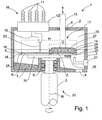
- FIGS. 1 and 2 each show a device for chemically removing a polymer layer 18, in particular a permanent photoresist, from a substrate 8, in particular a wafer.
- the components of the device listed below have the same structure or the same function, so that the structure and function first on the example of FIG. 1 to be discribed.
- the device consists of a housing 1, 1 ', which is composed of an upper part 2, 2' and a lower part 3 supporting the upper part 2, 2 '.
- the housing 1, 1 ' may alternatively be integrally formed with a lid or a side, closable opening.
- the housing 1, 1 ' encloses a working space 15, in which the polymer layer 18 is dissolved by the fluid 23.
- an outlet 4 is provided, is sucked through the superfluous fluid 23 or a mixture of the fluid 23 and the polymer layer 18 dissolved by the fluid 23, in particular by a vacuum device, not shown, which simultaneously for the Actuation of the working space 15 can be used with a vacuum.
- a vacuum device not shown, which simultaneously for the Actuation of the working space 15 can be used with a vacuum.
- the outlet 4 may also be provided a separator and / or a filter.
- the substrate 8 is received by a sample holder 24 of a substrate holder 22 and fixed by conventional means, for example provided on the surface of the sample holder 24 suction webs, in an aligned position.
- the aligned position means that a center Z of the substrate 8, in particular its centroid or geometric center lies on a rotation axis R of the substrate receptacle 22 rotatable by a shaft 5.
- the substrate 8 rests with its rear side 25 on the surface of the sample holder 24.
- the polymer layer 18 on an upper side 19 of the substrate 8 opposite the rear side 25 is wetted by the application means 16, 16 'with the fluid 23, in particular covered over its entire area.
- the application means 16, 16 'consist of lines 11 which introduce one or more substances and / or gases into a fluid reservoir 12 acting as a mixing chamber, wherein a specific quantitative ratio is predetermined by a controller (not shown) and / or adjustable. In the mixing chamber, a mixing of the liquids and / or gases to the fluid 23.
- Each of the lines 11 can advantageously by a preheater (not shown) to be heated to preheat the liquid or the gas to a predetermined temperature.
- the fluid 23 is applied via a feed line 10, 10 'on the polymer layer 18 and there distributed homogeneously or automatically by rotation of the substrate holder 22.
- sample holder 24 is formed so that the greatest possible heat insulation is provided relative to the substrate 8 or the sample holder 24 is provided with an additional heating device.
- the sample holder 24 has a plurality of voltage applied to the back 25 contact points, in particular formed by a spherical surface or a plurality of inserted in a trough of the sample holder balls 26, whereby the insulating effect with air or vacuum is optimized as an insulator.
- the sample holder 24 may be made at least partially of a material having a low thermal conductivity.
- the polymer layer 18 After application of the fluid 23 to the polymer layer 18, the polymer layer 18 is heated by heating means 17, 17 'to the optimum process temperature of the fluid 23.
- the heating means 17, 17 'consist of at least one guide arm 13, 13' which is perpendicular to a top 9 of the polymer layer 18 is moved, under the control of the control device.
- heating coils 27 it is possible in an alternative embodiment of the invention to provide an infrared or induction heating. It is crucial that the heating surface 20, 20 'contacts the fluid 23 applied to the polymer layer 18, preferably dips into the fluid.
- a distance measurement for measuring the distance between the heating surface 20, 20 'and the polymer layer 18 is provided on the heating device 14, 14'.
- the heating device 14 has a diameter D of approximately half the diameter H of the polymer layer 18.
- the heating surface 20 therefore extends in cross section over half the diameter H of the polymer layer 18, wherein an edge 28 of the heating surface 20 in the region of an edge 29 of the polymer layer 18 is arranged so that upon rotation of the substrate 8 through the substrate holder 22 about the rotation axis R at the latest after a complete revolution of the substrate 8 about the rotation axis R, the polymer layer 18 or the fluid 23 has been completely acted upon by the heating surface 20.
- the diameter D 'of the heating device 14' is approximately the same size as the diameter H of the polymer layer 18, so that the heating surface 20 'essentially speaks the surface of the upper side 9 of the polymer layer 18.
- the structure of the feed line 10 ' is more complicated, since in the embodiment shown, this passes through the heating device 14' in the region of the center Z, so that the fluid 23 can be applied to the polymer layer 18 approximately in the region of the center Z.
- the guide arms 13, 13 ' can be driven, for example, by linear motors, controlled by the control device, wherein the guide arms 13, 13' for the advantageous arrangement of the drives outside the working space 15, the housing 1, 1 'are arranged passing through. It is particularly advantageous to seal the guide arms 13, 13 'by seals 6, so that nothing can escape from the working space 15 in this way. At the same time, this minimizes the size of the working space 15 and makes it possible to apply a higher and constant vacuum.
- a gradient device 7 for generating a gradient here in the form of a slope, provided.
- the gradient device 7 can also be provided by appropriate shaping of the lower part 3.
- a cleaning of the substrate 8 takes place, in particular with water and / or solvents and / or chemicals intended for this purpose, which are applied by the application means 16, 16 '. be applied to the substrate 8.
- a separate application means for the cleaning liquid is provided in order not to contaminate the cleaning liquid by chemical residues of the fluid 23 in the application means 16, 16 '.
- a separate cleaning device 21 is provided for cleaning the underside of the substrate, in particular on the edge of the substrate 8, wherein the cleaning is preferably carried out at a location of the circumference of the substrate 8 during the rotation of the substrate 8 through the substrate receptacle 22.
- an inert gas in particular nitrogen, in order to avoid oxidation or ignition reactions due to the high temperatures.
Landscapes
- Engineering & Computer Science (AREA)
- Microelectronics & Electronic Packaging (AREA)
- Condensed Matter Physics & Semiconductors (AREA)
- General Physics & Mathematics (AREA)
- Manufacturing & Machinery (AREA)
- Computer Hardware Design (AREA)
- Physics & Mathematics (AREA)
- Power Engineering (AREA)
- Coating Apparatus (AREA)
- Exposure Of Semiconductors, Excluding Electron Or Ion Beam Exposure (AREA)
- Sampling And Sample Adjustment (AREA)
- Container, Conveyance, Adherence, Positioning, Of Wafer (AREA)
- Cleaning Or Drying Semiconductors (AREA)
Priority Applications (6)
| Application Number | Priority Date | Filing Date | Title |
|---|---|---|---|
| EP10004509.5A EP2383771B1 (fr) | 2010-04-29 | 2010-04-29 | Dispositif et procédé d'enlèvement d'une couche polymère de la surface d'un substrat |
| TW100110485A TWI546856B (zh) | 2010-04-29 | 2011-03-25 | 用於自一基板表面鬆脫ㄧ聚合物層之裝置及方法 |
| US13/078,110 US8828147B2 (en) | 2010-04-29 | 2011-04-01 | Device and method for loosening a polymer layer from a surface of a substrate |
| KR1020110032722A KR20110120820A (ko) | 2010-04-29 | 2011-04-08 | 기판의 표면으로부터 폴리머 층을 이완하는 장치 및 방법 |
| JP2011101245A JP2011233902A (ja) | 2010-04-29 | 2011-04-28 | 基板の表面からポリマー層を剥離するための装置および方法 |
| CN201110110531.2A CN102237261B (zh) | 2010-04-29 | 2011-04-29 | 从基板表面松动聚合物层的设备和方法 |
Applications Claiming Priority (1)
| Application Number | Priority Date | Filing Date | Title |
|---|---|---|---|
| EP10004509.5A EP2383771B1 (fr) | 2010-04-29 | 2010-04-29 | Dispositif et procédé d'enlèvement d'une couche polymère de la surface d'un substrat |
Publications (2)
| Publication Number | Publication Date |
|---|---|
| EP2383771A1 true EP2383771A1 (fr) | 2011-11-02 |
| EP2383771B1 EP2383771B1 (fr) | 2020-04-22 |
Family
ID=42357215
Family Applications (1)
| Application Number | Title | Priority Date | Filing Date |
|---|---|---|---|
| EP10004509.5A Active EP2383771B1 (fr) | 2010-04-29 | 2010-04-29 | Dispositif et procédé d'enlèvement d'une couche polymère de la surface d'un substrat |
Country Status (6)
| Country | Link |
|---|---|
| US (1) | US8828147B2 (fr) |
| EP (1) | EP2383771B1 (fr) |
| JP (1) | JP2011233902A (fr) |
| KR (1) | KR20110120820A (fr) |
| CN (1) | CN102237261B (fr) |
| TW (1) | TWI546856B (fr) |
Families Citing this family (7)
| Publication number | Priority date | Publication date | Assignee | Title |
|---|---|---|---|---|
| JP2013182958A (ja) * | 2012-02-29 | 2013-09-12 | Dainippon Screen Mfg Co Ltd | 基板処理方法 |
| JP5852927B2 (ja) * | 2012-06-27 | 2016-02-03 | 株式会社Screenホールディングス | 基板処理方法 |
| CN103295936B (zh) * | 2012-02-29 | 2016-01-13 | 斯克林集团公司 | 基板处理装置及基板处理方法 |
| JP6227131B2 (ja) * | 2013-07-04 | 2017-11-08 | エーファウ・グループ・エー・タルナー・ゲーエムベーハー | 基材表面の処理方法および装置 |
| JP6222818B2 (ja) * | 2013-09-10 | 2017-11-01 | 株式会社Screenホールディングス | 基板処理方法および基板処理装置 |
| KR102182068B1 (ko) | 2020-07-09 | 2020-11-23 | (주)서울환경 | 도장용 분진포집장치 |
| KR102181817B1 (ko) | 2020-07-09 | 2020-11-24 | 이지창 | 도장용 분진포집장치 |
Citations (8)
| Publication number | Priority date | Publication date | Assignee | Title |
|---|---|---|---|---|
| US20020033183A1 (en) | 1999-05-29 | 2002-03-21 | Sheng Sun | Method and apparatus for enhanced chamber cleaning |
| US20030183246A1 (en) * | 2002-03-29 | 2003-10-02 | Lam Research Corporation | In-situ local heating using megasonic transducer resonator |
| US20040211442A1 (en) * | 2003-04-22 | 2004-10-28 | Changfeng Xia | Method and apparatus for removing polymer residue from semiconductor wafer edge and back side |
| US6847014B1 (en) * | 2001-04-30 | 2005-01-25 | Lam Research Corporation | Method and apparatus for controlling the spatial temperature distribution across the surface of a workpiece support |
| US20050205521A1 (en) * | 2004-03-17 | 2005-09-22 | Semiconductor Leading Edge Technologies, Inc. | Wet etching apparatus and wet etching method |
| EP1583135A1 (fr) * | 2004-03-31 | 2005-10-05 | Lam Research | Un procédé et un appareil de chauffage dans les têtes de proximité pour la fabrication de plaquettes semiconductrices |
| US20070163711A1 (en) * | 2006-01-13 | 2007-07-19 | Kyo-Woog Koo | Apparatus for treating substrate |
| US20080072925A1 (en) * | 2006-08-04 | 2008-03-27 | Samsung Electronics Co., Ltd. | Wafer cleaning apparatus |
Family Cites Families (12)
| Publication number | Priority date | Publication date | Assignee | Title |
|---|---|---|---|---|
| JPS61104621A (ja) * | 1984-10-29 | 1986-05-22 | Nec Corp | ポジレジスト現像装置 |
| JPH09134872A (ja) * | 1995-11-08 | 1997-05-20 | Nippon Steel Corp | レジスト剥離方法及び装置 |
| JPH10135127A (ja) * | 1996-10-31 | 1998-05-22 | Canon Sales Co Inc | 基板現像装置 |
| US6073681A (en) * | 1997-12-31 | 2000-06-13 | Temptronic Corporation | Workpiece chuck |
| JP2001007017A (ja) * | 1999-04-21 | 2001-01-12 | Sharp Corp | レジスト剥離装置 |
| CN100401852C (zh) * | 2001-04-30 | 2008-07-09 | 科林研发公司 | 用于控制工件支架表面上空间温度分布的方法与装置 |
| JP4038556B2 (ja) * | 2002-04-16 | 2008-01-30 | リアライズ・アドバンストテクノロジ株式会社 | レジスト膜除去装置及びレジスト膜除去方法、並びに有機物除去装置及び有機物除去方法 |
| JP2006108304A (ja) * | 2004-10-04 | 2006-04-20 | Nec Electronics Corp | 基板処理装置 |
| US20060254612A1 (en) * | 2005-05-16 | 2006-11-16 | Micron Technology, Inc. | Polar fluid removal from surfaces using supercritical fluids |
| US20110070370A1 (en) * | 2008-05-28 | 2011-03-24 | Aixtron Ag | Thermal gradient enhanced chemical vapour deposition (tge-cvd) |
| US20110139183A1 (en) * | 2009-12-11 | 2011-06-16 | Katrina Mikhaylichenko | System and method of preventing pattern collapse using low surface tension fluid |
| CN102782807B (zh) * | 2010-01-22 | 2015-07-08 | 芝浦机械电子装置股份有限公司 | 基板处理装置及基板处理方法 |
-
2010
- 2010-04-29 EP EP10004509.5A patent/EP2383771B1/fr active Active
-
2011
- 2011-03-25 TW TW100110485A patent/TWI546856B/zh active
- 2011-04-01 US US13/078,110 patent/US8828147B2/en active Active
- 2011-04-08 KR KR1020110032722A patent/KR20110120820A/ko not_active Application Discontinuation
- 2011-04-28 JP JP2011101245A patent/JP2011233902A/ja active Pending
- 2011-04-29 CN CN201110110531.2A patent/CN102237261B/zh active Active
Patent Citations (8)
| Publication number | Priority date | Publication date | Assignee | Title |
|---|---|---|---|---|
| US20020033183A1 (en) | 1999-05-29 | 2002-03-21 | Sheng Sun | Method and apparatus for enhanced chamber cleaning |
| US6847014B1 (en) * | 2001-04-30 | 2005-01-25 | Lam Research Corporation | Method and apparatus for controlling the spatial temperature distribution across the surface of a workpiece support |
| US20030183246A1 (en) * | 2002-03-29 | 2003-10-02 | Lam Research Corporation | In-situ local heating using megasonic transducer resonator |
| US20040211442A1 (en) * | 2003-04-22 | 2004-10-28 | Changfeng Xia | Method and apparatus for removing polymer residue from semiconductor wafer edge and back side |
| US20050205521A1 (en) * | 2004-03-17 | 2005-09-22 | Semiconductor Leading Edge Technologies, Inc. | Wet etching apparatus and wet etching method |
| EP1583135A1 (fr) * | 2004-03-31 | 2005-10-05 | Lam Research | Un procédé et un appareil de chauffage dans les têtes de proximité pour la fabrication de plaquettes semiconductrices |
| US20070163711A1 (en) * | 2006-01-13 | 2007-07-19 | Kyo-Woog Koo | Apparatus for treating substrate |
| US20080072925A1 (en) * | 2006-08-04 | 2008-03-27 | Samsung Electronics Co., Ltd. | Wafer cleaning apparatus |
Also Published As
| Publication number | Publication date |
|---|---|
| TWI546856B (zh) | 2016-08-21 |
| US20110265822A1 (en) | 2011-11-03 |
| JP2011233902A (ja) | 2011-11-17 |
| CN102237261B (zh) | 2015-10-21 |
| CN102237261A (zh) | 2011-11-09 |
| TW201203345A (en) | 2012-01-16 |
| EP2383771B1 (fr) | 2020-04-22 |
| US8828147B2 (en) | 2014-09-09 |
| KR20110120820A (ko) | 2011-11-04 |
Similar Documents
| Publication | Publication Date | Title |
|---|---|---|
| EP2383771A1 (fr) | Dispositif et procédé d'enlèvement d'une couche polymère de la surface d'un substrat | |
| EP1948845B1 (fr) | Reacteur de depot chimique en phase vapeur a support de substrat monte coulissant | |
| DE19818529B4 (de) | Photoresistbeschichtungsverfahren und Vorrichtung zur Durchführung dieses Verfahrens | |
| EP0592654B2 (fr) | Dispositif pour traiter par evaporation des substances de preferance liquides, notamment des substance reactives, ou bien pour preparer ou analyser des prelevements | |
| WO1991012790A1 (fr) | Dispositif d'enduction avec une pellicule ou avec du sucre | |
| EP1297561B1 (fr) | Procede et dispositif d'epuration et de metallisation successive de substrats | |
| EP1743220B1 (fr) | Dispositif de revetement rotatif de substrats | |
| EP1374991B1 (fr) | Mélangement et réactions de solides, suspensions et emulsions avec des micro-ondes | |
| EP1959301A1 (fr) | Dispositif et procédé pour l'étalement d'un revêtement par force centrifuge | |
| DE102018207252B4 (de) | Waferbearbeitungsverfahren | |
| WO2008043463A1 (fr) | Dispositif et procédé de fabrication d'une station pour formuler des formulations de substances | |
| DE2854551A1 (de) | Maschine zum zerschneiden von stangen in scheiben | |
| EP2630653B1 (fr) | Dispositif de revêtement d'une tranche | |
| DE69133335T2 (de) | Vorrichtung zur Behandlung von Wafern | |
| DE102005025469B4 (de) | Verfahren und Vorrichtung zum Aufbringen einer Materialschicht auf elektrische Komponenten | |
| DE102007057297A1 (de) | Elektrolytische Aufbereitungsvorrichtung und Verfahren zur elektrolytischen Aufbereitung, zum Waschen und Trocknen | |
| DE102005059850A1 (de) | Vorrichtung zum Reinigen und Trocknen von Wafern | |
| DE4003119C2 (fr) | ||
| EP2758991B1 (fr) | Dispositif et procede de traitement de surfaces de substrats | |
| DE4325667A1 (de) | Behälteranordnung mit einem Behälter zur Verdampfungsbehandlung oder zur Aufbereitung und Analyse von Stoffen | |
| WO2015124144A1 (fr) | Dispositif de traitement chimique par voie humide d'objets, en particulier d'objets plats, en particulier en forme de disques tels que des tranches de semi-conducteur, des substrats ou similaires | |
| EP3644752A1 (fr) | Dispositif conçu pour pasteuriser une matière de type crème glacée | |
| EP2624291B1 (fr) | Dispositif de traitement d'un substrat et procédé pour ce faire | |
| DE10144874B4 (de) | Verfahren und Vorrichtung zum homogenen Auftragen einer Lackschicht auf vorvereinzelte Substrate | |
| DE10058131A1 (de) | Verfahren zum Beschichten von Apparaten und Apparateteilen |
Legal Events
| Date | Code | Title | Description |
|---|---|---|---|
| AK | Designated contracting states |
Kind code of ref document: A1 Designated state(s): AT BE BG CH CY CZ DE DK EE ES FI FR GB GR HR HU IE IS IT LI LT LU LV MC MK MT NL NO PL PT RO SE SI SK SM TR |
|
| AX | Request for extension of the european patent |
Extension state: AL BA ME RS |
|
| PUAI | Public reference made under article 153(3) epc to a published international application that has entered the european phase |
Free format text: ORIGINAL CODE: 0009012 |
|
| 17P | Request for examination filed |
Effective date: 20111102 |
|
| 17Q | First examination report despatched |
Effective date: 20121001 |
|
| STAA | Information on the status of an ep patent application or granted ep patent |
Free format text: STATUS: EXAMINATION IS IN PROGRESS |
|
| REG | Reference to a national code |
Ref country code: DE Ref legal event code: R079 Ref document number: 502010016591 Country of ref document: DE Free format text: PREVIOUS MAIN CLASS: H01L0021000000 Ipc: H01L0021670000 |
|
| GRAP | Despatch of communication of intention to grant a patent |
Free format text: ORIGINAL CODE: EPIDOSNIGR1 |
|
| STAA | Information on the status of an ep patent application or granted ep patent |
Free format text: STATUS: GRANT OF PATENT IS INTENDED |
|
| RIC1 | Information provided on ipc code assigned before grant |
Ipc: H01L 21/67 20060101AFI20191129BHEP |
|
| INTG | Intention to grant announced |
Effective date: 20191219 |
|
| RIN1 | Information on inventor provided before grant (corrected) |
Inventor name: HOLZLEITNER, RONALD Inventor name: LINDNER, PAUL Inventor name: CROWDER, MATT Inventor name: THALLNER, ERICH Inventor name: GLINSNER, THOMAS |
|
| GRAS | Grant fee paid |
Free format text: ORIGINAL CODE: EPIDOSNIGR3 |
|
| GRAA | (expected) grant |
Free format text: ORIGINAL CODE: 0009210 |
|
| STAA | Information on the status of an ep patent application or granted ep patent |
Free format text: STATUS: THE PATENT HAS BEEN GRANTED |
|
| AK | Designated contracting states |
Kind code of ref document: B1 Designated state(s): AT BE BG CH CY CZ DE DK EE ES FI FR GB GR HR HU IE IS IT LI LT LU LV MC MK MT NL NO PL PT RO SE SI SK SM TR |
|
| REG | Reference to a national code |
Ref country code: GB Ref legal event code: FG4D Free format text: NOT ENGLISH |
|
| REG | Reference to a national code |
Ref country code: CH Ref legal event code: EP |
|
| REG | Reference to a national code |
Ref country code: DE Ref legal event code: R096 Ref document number: 502010016591 Country of ref document: DE |
|
| REG | Reference to a national code |
Ref country code: IE Ref legal event code: FG4D Free format text: LANGUAGE OF EP DOCUMENT: GERMAN |
|
| REG | Reference to a national code |
Ref country code: AT Ref legal event code: REF Ref document number: 1261249 Country of ref document: AT Kind code of ref document: T Effective date: 20200515 |
|
| REG | Reference to a national code |
Ref country code: LT Ref legal event code: MG4D |
|
| REG | Reference to a national code |
Ref country code: NL Ref legal event code: MP Effective date: 20200422 |
|
| PG25 | Lapsed in a contracting state [announced via postgrant information from national office to epo] |
Ref country code: SE Free format text: LAPSE BECAUSE OF FAILURE TO SUBMIT A TRANSLATION OF THE DESCRIPTION OR TO PAY THE FEE WITHIN THE PRESCRIBED TIME-LIMIT Effective date: 20200422 Ref country code: IS Free format text: LAPSE BECAUSE OF FAILURE TO SUBMIT A TRANSLATION OF THE DESCRIPTION OR TO PAY THE FEE WITHIN THE PRESCRIBED TIME-LIMIT Effective date: 20200822 Ref country code: FI Free format text: LAPSE BECAUSE OF FAILURE TO SUBMIT A TRANSLATION OF THE DESCRIPTION OR TO PAY THE FEE WITHIN THE PRESCRIBED TIME-LIMIT Effective date: 20200422 Ref country code: GR Free format text: LAPSE BECAUSE OF FAILURE TO SUBMIT A TRANSLATION OF THE DESCRIPTION OR TO PAY THE FEE WITHIN THE PRESCRIBED TIME-LIMIT Effective date: 20200723 Ref country code: NO Free format text: LAPSE BECAUSE OF FAILURE TO SUBMIT A TRANSLATION OF THE DESCRIPTION OR TO PAY THE FEE WITHIN THE PRESCRIBED TIME-LIMIT Effective date: 20200722 Ref country code: NL Free format text: LAPSE BECAUSE OF FAILURE TO SUBMIT A TRANSLATION OF THE DESCRIPTION OR TO PAY THE FEE WITHIN THE PRESCRIBED TIME-LIMIT Effective date: 20200422 Ref country code: PT Free format text: LAPSE BECAUSE OF FAILURE TO SUBMIT A TRANSLATION OF THE DESCRIPTION OR TO PAY THE FEE WITHIN THE PRESCRIBED TIME-LIMIT Effective date: 20200824 Ref country code: LT Free format text: LAPSE BECAUSE OF FAILURE TO SUBMIT A TRANSLATION OF THE DESCRIPTION OR TO PAY THE FEE WITHIN THE PRESCRIBED TIME-LIMIT Effective date: 20200422 |
|
| PG25 | Lapsed in a contracting state [announced via postgrant information from national office to epo] |
Ref country code: LV Free format text: LAPSE BECAUSE OF FAILURE TO SUBMIT A TRANSLATION OF THE DESCRIPTION OR TO PAY THE FEE WITHIN THE PRESCRIBED TIME-LIMIT Effective date: 20200422 Ref country code: BG Free format text: LAPSE BECAUSE OF FAILURE TO SUBMIT A TRANSLATION OF THE DESCRIPTION OR TO PAY THE FEE WITHIN THE PRESCRIBED TIME-LIMIT Effective date: 20200722 Ref country code: HR Free format text: LAPSE BECAUSE OF FAILURE TO SUBMIT A TRANSLATION OF THE DESCRIPTION OR TO PAY THE FEE WITHIN THE PRESCRIBED TIME-LIMIT Effective date: 20200422 |
|
| REG | Reference to a national code |
Ref country code: CH Ref legal event code: PL |
|
| REG | Reference to a national code |
Ref country code: DE Ref legal event code: R097 Ref document number: 502010016591 Country of ref document: DE |
|
| PG25 | Lapsed in a contracting state [announced via postgrant information from national office to epo] |
Ref country code: CH Free format text: LAPSE BECAUSE OF NON-PAYMENT OF DUE FEES Effective date: 20200430 Ref country code: LI Free format text: LAPSE BECAUSE OF NON-PAYMENT OF DUE FEES Effective date: 20200430 Ref country code: DK Free format text: LAPSE BECAUSE OF FAILURE TO SUBMIT A TRANSLATION OF THE DESCRIPTION OR TO PAY THE FEE WITHIN THE PRESCRIBED TIME-LIMIT Effective date: 20200422 Ref country code: MC Free format text: LAPSE BECAUSE OF FAILURE TO SUBMIT A TRANSLATION OF THE DESCRIPTION OR TO PAY THE FEE WITHIN THE PRESCRIBED TIME-LIMIT Effective date: 20200422 Ref country code: ES Free format text: LAPSE BECAUSE OF FAILURE TO SUBMIT A TRANSLATION OF THE DESCRIPTION OR TO PAY THE FEE WITHIN THE PRESCRIBED TIME-LIMIT Effective date: 20200422 Ref country code: RO Free format text: LAPSE BECAUSE OF FAILURE TO SUBMIT A TRANSLATION OF THE DESCRIPTION OR TO PAY THE FEE WITHIN THE PRESCRIBED TIME-LIMIT Effective date: 20200422 Ref country code: CZ Free format text: LAPSE BECAUSE OF FAILURE TO SUBMIT A TRANSLATION OF THE DESCRIPTION OR TO PAY THE FEE WITHIN THE PRESCRIBED TIME-LIMIT Effective date: 20200422 Ref country code: LU Free format text: LAPSE BECAUSE OF NON-PAYMENT OF DUE FEES Effective date: 20200429 Ref country code: EE Free format text: LAPSE BECAUSE OF FAILURE TO SUBMIT A TRANSLATION OF THE DESCRIPTION OR TO PAY THE FEE WITHIN THE PRESCRIBED TIME-LIMIT Effective date: 20200422 Ref country code: SM Free format text: LAPSE BECAUSE OF FAILURE TO SUBMIT A TRANSLATION OF THE DESCRIPTION OR TO PAY THE FEE WITHIN THE PRESCRIBED TIME-LIMIT Effective date: 20200422 Ref country code: IT Free format text: LAPSE BECAUSE OF FAILURE TO SUBMIT A TRANSLATION OF THE DESCRIPTION OR TO PAY THE FEE WITHIN THE PRESCRIBED TIME-LIMIT Effective date: 20200422 |
|
| REG | Reference to a national code |
Ref country code: BE Ref legal event code: MM Effective date: 20200430 |
|
| PG25 | Lapsed in a contracting state [announced via postgrant information from national office to epo] |
Ref country code: PL Free format text: LAPSE BECAUSE OF FAILURE TO SUBMIT A TRANSLATION OF THE DESCRIPTION OR TO PAY THE FEE WITHIN THE PRESCRIBED TIME-LIMIT Effective date: 20200422 Ref country code: BE Free format text: LAPSE BECAUSE OF NON-PAYMENT OF DUE FEES Effective date: 20200430 Ref country code: SK Free format text: LAPSE BECAUSE OF FAILURE TO SUBMIT A TRANSLATION OF THE DESCRIPTION OR TO PAY THE FEE WITHIN THE PRESCRIBED TIME-LIMIT Effective date: 20200422 |
|
| PLBE | No opposition filed within time limit |
Free format text: ORIGINAL CODE: 0009261 |
|
| STAA | Information on the status of an ep patent application or granted ep patent |
Free format text: STATUS: NO OPPOSITION FILED WITHIN TIME LIMIT |
|
| 26N | No opposition filed |
Effective date: 20210125 |
|
| GBPC | Gb: european patent ceased through non-payment of renewal fee |
Effective date: 20200722 |
|
| PG25 | Lapsed in a contracting state [announced via postgrant information from national office to epo] |
Ref country code: IE Free format text: LAPSE BECAUSE OF NON-PAYMENT OF DUE FEES Effective date: 20200429 Ref country code: FR Free format text: LAPSE BECAUSE OF NON-PAYMENT OF DUE FEES Effective date: 20200622 Ref country code: GB Free format text: LAPSE BECAUSE OF NON-PAYMENT OF DUE FEES Effective date: 20200722 |
|
| PG25 | Lapsed in a contracting state [announced via postgrant information from national office to epo] |
Ref country code: SI Free format text: LAPSE BECAUSE OF FAILURE TO SUBMIT A TRANSLATION OF THE DESCRIPTION OR TO PAY THE FEE WITHIN THE PRESCRIBED TIME-LIMIT Effective date: 20200422 |
|
| PG25 | Lapsed in a contracting state [announced via postgrant information from national office to epo] |
Ref country code: TR Free format text: LAPSE BECAUSE OF FAILURE TO SUBMIT A TRANSLATION OF THE DESCRIPTION OR TO PAY THE FEE WITHIN THE PRESCRIBED TIME-LIMIT Effective date: 20200422 Ref country code: MT Free format text: LAPSE BECAUSE OF FAILURE TO SUBMIT A TRANSLATION OF THE DESCRIPTION OR TO PAY THE FEE WITHIN THE PRESCRIBED TIME-LIMIT Effective date: 20200422 Ref country code: CY Free format text: LAPSE BECAUSE OF FAILURE TO SUBMIT A TRANSLATION OF THE DESCRIPTION OR TO PAY THE FEE WITHIN THE PRESCRIBED TIME-LIMIT Effective date: 20200422 |
|
| PG25 | Lapsed in a contracting state [announced via postgrant information from national office to epo] |
Ref country code: MK Free format text: LAPSE BECAUSE OF FAILURE TO SUBMIT A TRANSLATION OF THE DESCRIPTION OR TO PAY THE FEE WITHIN THE PRESCRIBED TIME-LIMIT Effective date: 20200422 |
|
| PGFP | Annual fee paid to national office [announced via postgrant information from national office to epo] |
Ref country code: DE Payment date: 20230427 Year of fee payment: 14 |
|
| PGFP | Annual fee paid to national office [announced via postgrant information from national office to epo] |
Ref country code: AT Payment date: 20230414 Year of fee payment: 14 |