EP2378446A2 - Gekoppelte Analysesimulationsvorrichtung und gekoppeltes Analysesimulationsverfahren - Google Patents
Gekoppelte Analysesimulationsvorrichtung und gekoppeltes Analysesimulationsverfahren Download PDFInfo
- Publication number
- EP2378446A2 EP2378446A2 EP10178437A EP10178437A EP2378446A2 EP 2378446 A2 EP2378446 A2 EP 2378446A2 EP 10178437 A EP10178437 A EP 10178437A EP 10178437 A EP10178437 A EP 10178437A EP 2378446 A2 EP2378446 A2 EP 2378446A2
- Authority
- EP
- European Patent Office
- Prior art keywords
- analysis
- virtual
- electronic circuit
- conductive part
- coupled
- Prior art date
- Legal status (The legal status is an assumption and is not a legal conclusion. Google has not performed a legal analysis and makes no representation as to the accuracy of the status listed.)
- Withdrawn
Links
Images















Classifications
-
- G—PHYSICS
- G06—COMPUTING OR CALCULATING; COUNTING
- G06F—ELECTRIC DIGITAL DATA PROCESSING
- G06F30/00—Computer-aided design [CAD]
- G06F30/30—Circuit design
- G06F30/36—Circuit design at the analogue level
- G06F30/367—Design verification, e.g. using simulation, simulation program with integrated circuit emphasis [SPICE], direct methods or relaxation methods
-
- G—PHYSICS
- G06—COMPUTING OR CALCULATING; COUNTING
- G06F—ELECTRIC DIGITAL DATA PROCESSING
- G06F30/00—Computer-aided design [CAD]
Definitions
- Electromagnetic field analysis simulators are for performing EMC (Electro-Magnetic Compatibility) analysis on a PCB (Printed Circuit Board) on which electronic circuit modules are mounted.
- the EMC analysis is performed by various methods such as an FDTD (Finite-Difference Time-Domain) method, a moment method, and a TLM (Transmission-Line Matrix) method.
- FDTD Finite-Difference Time-Domain
- moment method a moment method
- TLM Transmission-Line Matrix
- a circuit analysis unit obtains the voltage value of the coupling device with the use of the current value of the coupling device, converts the obtained voltage value into an electric field value of the cell in which the coupling device is present, and passes the electric field value to an electromagnetic field analysis unit. Furthermore, the electromagnetic field analysis unit obtains the magnetic field from the electric field value of the cell in which the coupling device is present, converts the obtained magnetic field into a current value that flows into the coupling device, and passes the current value to the circuit analysis unit.
- a computer-readable recording medium records a coupled analysis simulation program that causes a computer to function as a coupled analysis processing unit configured to perform coupled analysis by performing electromagnetic field analysis and circuit analysis in coordination with each other, the electromagnetic field analysis being performed on a space including conductive layers to which an electronic circuit module is connected, the circuit analysis being performed on the electronic circuit module; a first generating unit configured to generate a virtual conductive part in a section or a region including connection parts connecting the electronic circuit module with the conductive layers; and a second generating unit configured to generate virtual connection parts that virtually connect the virtual conductive part with the conductive layers at positions where the connection parts are connected to the conductive layers.
- FIG. 2 is a block diagram of relevant parts of the main unit 11 of the computer system 10.
- the main unit 11 includes a CPU 21, a memory unit 22 including a RAM or a ROM, a disk drive 23 for the disk 17, and a hard disk drive (HDD) 24, which are connected to each other by a bus 20.
- CAD Computer Aided Design
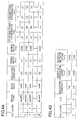
- the CAD data indicated in FIG. 4A includes the identifier (No.) of the wiring, the layer number, the signal type, the data rate, the dielectric constant, the wiring width, the wiring height, starting point coordinates, and ending point coordinates.
- the starting points and ending points are expressed by using a coordinate system defined for the printed circuit board.
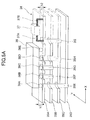
- FIGS. 5A and 5B illustrate the relationship between the virtual conductive parts/coupling devices and the electronic circuit modules/terminals.
- FIG. 5A schematically illustrates the connection relationship between the electronic circuit modules and the conductive layers mounted on the printed circuit board.
- FIG. 5B illustrates virtual conductive parts and coupling devices generated by modeling the electronic circuit modules and the conductive layers illustrated in FIG. 5A .
- the coupled analysis simulation apparatus uses coupling devices 101 through 107 and virtual conductive parts 111 and 112.
- the bumps 38A through 38E and the terminals 37A and 37B acting as connection parts between the LSI 36 or the bypass capacitor 37 and the conductive layers 35A through 35D illustrated in FIG. 5A are modeled and defined as the coupling devices 101 through 107.
- the coupling devices 101 through 107 are virtual connection parts.
- the coupling devices 101 through 107 include terminals 101A through 107A that are connected to the conductive layers (35A through 35D) before being modeled.
- the coupling devices 101 through 107 also include terminals 101B through 107B that are connected to the virtual conductive parts 111 and 112.
- the coupling devices 101 through 107 which are two-terminal devices that are embodiments of the virtual connection parts, are used for connecting the conductive layers 35A through 35D to the virtual conductive parts 111 and 112.
- the coupling devices 101 through 107 are defined as perfect conductors. In this example, perfect conductors have an electric resistance of zero.
- the coupling devices 101 through 107 and the virtual conductive parts 111 and 112 are defined as perfect conductors; however, the coupling devices 101 through 107 and the virtual conductive parts 111 and 112 may be defined as conductors other than perfect conductors.
- the virtual conductive part 111 is connected to the coupling devices 101 through 105 that are generated by modeling the bumps 38A through 38E (see FIG. 5A ) that are arranged linearly, and therefore the virtual conductive part 111 is defined as a linear perfect conductor as a matter of convenience. Furthermore, the virtual conductive part 112 is connected to two coupling devices 106 and 107 that are generated by modeling the terminals 37A and 37B of the bypass capacitor 37 that is a simplified two-terminal device, and therefore the virtual conductive part 112 is defined as a linear perfect conductor as a matter of convenience.
- connection parts of an electronic circuit module are typically arranged in a planar manner (two-dimensionally). Therefore, in the process of generating a virtual conductive part described with reference to a flowchart of FIG. 7 , a description is given of a process of generating a planar virtual conductive part.
- the coupling devices 101 through 107 may be referred to as coupling devices 100, when the coupling devices 101 through 107 are not particularly distinguished from one another.
- the virtual conductive parts 111 and 112 may be referred to as virtual conductive parts 110.
- FIG. 6 is a block diagram of processing units included in the coupled analysis simulation apparatus according to the first embodiment of the present invention.
- the processing units illustrated in FIG. 6 are implemented as the CPU 21 illustrated in FIG. 2 executes the coupled analysis simulation program stored in the HDD 24.
- the main control unit 211 controls the processing units of the design data reading unit 212 through the data management unit 219, and causes these processing units to execute processes.
- the design data reading unit 212 reads the CAD data that is stored in the HDD 24.
- the virtual connection part generating unit 215 generates the coupling device 100 that is an embodiment of the virtual connection part connecting the virtual conductive part 110, which is generated by the virtual conductive part generating unit 214, to the conductive layers 35. Details of the generating method are described with reference to the flowchart of FIG. 7 .
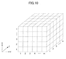
- the analysis model is a spatial model formed by dividing parts of the printed circuit board 34, the conductive layers 35, and the virtual conductive parts 110 included in the analysis region(three-dimensional space), by the division number in the X, Y, and Z axis directions, so that cells are formed as a result of the division.
- the electromagnetic field analysis is performed upon defining the virtual conductive parts 110 and the coupling devices 100 in the region where the electronic circuit modules and terminals are present.
- the analysis model includes the virtual conductive parts 110 and the coupling devices 100 corresponding to the electronic circuit modules and terminals that are the analysis objects. A description is given of the analysis model with reference to FIG. 10 .
- the coupled analysis processing unit 217 includes the coupled analysis control unit 221, the electromagnetic field analysis unit 222, the current calculation unit 223, the current transfer unit 224, the circuit analysis unit 225, the electric field calculation unit 226, and the electric field transfer unit 227; and performs coupled analysis in which electromagnetic field analysis and circuit analysis are performed in coordination with each other. Details of coupled analysis are described with reference to FIGS. 12 through 14 .
- the analysis result display processing unit 218 causes the display screen 12A of the display 12 illustrated in FIG. 1 to display analysis results obtained by the coupled analysis performed by the electromagnetic field analysis unit 222 and the circuit analysis unit 225.
- An example of analysis results is a return path obtained by coupled analysis. A description is given of a return path with reference to FIGS. 18 and 20 .
- the data management unit 219 is for managing the operations of storing data in the HDD 24.
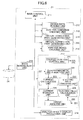
- FIG. 7 is a flowchart of a process for generating virtual conductive parts and coupling devices performed by the coupled analysis simulation apparatus according to the first embodiment of the present invention.
- the process illustrated in FIG. 7 is what the main control unit 211 inside the CPU 21 causes the virtual conductive part generating unit 214 and the virtual connection part generating unit 215 to execute. This process is executed according to analysis conditions created by the analysis condition creating unit 213.
- the process illustrated in FIG. 7 is applied to a case of generating the planar virtual conductive part 110 that is specified by four vertices. Coordinates of the four vertices are (Xmin, Ymin), (Xmin, Ymax), (Xmax, Ymin), and (Xmax, Ymax).
- the layer number of the LSI 36 is read, so that the virtual conductive part generating unit 214 recognizes whether the LSI 36 is mounted on the conductive layer 35A that is the topmost layer or the conductive layer 35D that is the bottommost layer.
- the virtual conductive part generating unit 214 specifies the X, Y coordinates of the terminal having the smallest terminal number among the terminals indicated in the analysis conditions, as the initial X, Y coordinates expressing the position of the virtual conductive part 110 (step S3) .
- the virtual conductive part generating unit 214 reads, from the CAD data, the coordinates (Xti, Yti) of the terminal having the next smallest terminal number (step S4), For example, when the virtual conductive part generating unit 214 has read, in step S3, the coordinates (Xt1, Yt1) of terminal 1 of the electronic circuit module having an identifier (No.) 1 indicated in FIG. 4C , in step S4, the virtual conductive part generating unit 214 reads coordinates (Xt2, Yt2) of terminal 2.
- step S11 When the virtual conductive part generating unit 214 determines that Ymin > Yti is satisfied in step S11 (Yes in step S11), the virtual conductive part generating unit 214 sets Yti as Ymin (step S12). Accordingly, the value of Ymin is updated to an even smaller value Yti.
- step S4 when the LSI 36 illustrated in FIG. 5A is selected in step S4, and the bumps 38A through 38E are specified as the terminals of the LSI 36 in the analysis conditions, the four vertices of the virtual conductive part 111 illustrated in FIG. 5B are determined. Definitions of the coupling devices 101 through 105 illustrated in FIG. 5B are described together with the process of step S20.
- the virtual conductive part generating unit 214 reads the height (h) of the electronic circuit module from the CAD data (step S16). This step is performed to set the height between the virtual conductive part 110 and the front surface (or back surface) of the printed circuit board 34 to be the same as the height of the electronic circuit module.
- the data expressing the height of the electronic circuit module is included in the CAD data indicated in FIG. 4C .
- the virtual conductive part generating unit 214 determines whether the electronic circuit module is mounted on the topmost layer (step S17). This step is performed because the direction of the height of the electronic circuit module differs depending on whether the electronic circuit module is mounted on the topmost layer or the bottommost layer. The determination of step S17 is made based on the layer number read in step S2.
- step S18B a value, which is obtained by subtracting the height (h) obtained in step S16 from the height of the bottommost conductive layer 35 (height of bottommost layer - h), is set as the height of the virtual conductive part 110 (step S18B).
- the virtual connection part generating unit 215 determines whether the terminal defining the coupling device 100 processed in step S20 is the last terminal (step S21).
- the terminals included in the analysis conditions are selected one by one to define each coupling device, and the selected terminal is processed in step S20. Therefore, step S20 is repeatedly performed until it is determined in step S21 that the processed terminal is the last terminal.
- the virtual conductive part generating unit 214 determines whether the processed electronic circuit module is the last electronic circuit module included in the analysis conditions (step S23).
- the virtual conductive part generating unit 214 determines that the processed electronic circuit module is not the last electronic circuit module, the virtual conductive part generating unit 214 reads the CAD data of the next electronic circuit module included in the analysis conditions (step S24).
- FIG. 7 illustrates the process of generating the virtual conductive parts 110 and the coupling devices 100, including determining the X, Y coordinates of the virtual conductive part 110 by executing steps S3 through S14, determining the height of each of the virtual conductive parts 110 by executing step S18A or S18B, and then defining the coupling devices 100.
- the process of generating the virtual conductive parts 110 and the coupling devices 100 performed by the coupled analysis simulation apparatus according to the first embodiment of the present invention is not limited to the order of the process as illustrated in FIG. 7 .
- the coupling devices 100 may be defined before defining the virtual conductive parts 110. Specifically, by repeating steps S20 and S21, the positions of the terminals included in the analysis conditions are recognized as positions where the coupling devices 100 are to be generated, and the coupling devices 100 are defined first by associating the heights of the electronic circuit modules with the recognized positions. Next, by executing steps S3 through S14, the virtual conductive parts 110 to be connected to the coupling devices 100 are defined.
- the layer number expresses whether the virtual conductive part 110 is to be defined on the topmost layer or the bottommost layer, and the height is expressed as +h or -h, where +h expresses the height from the topmost conductive layer 35 and -h expresses the height from the bottommost conductive layer 35.
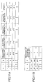
- the data indicated in FIG. 11B in which the identifier of the coupling device is associated with coordinates in the analysis model, is obtained by cross-checking and associating the information relevant to the identifier of the coupling device and the terminal included in a net list of the electronic circuit module, with the coordinates of the terminal included in the CAD data indicated in FIG. 4C .
- Alphanumeric symbols are used for expressing the dielectric constant, the electric conductivity, the magnetic permeability, the magnetic resistivity, and the density in FIG. 11A , and the (X, Y, Z) coordinates in FIG. 11B ; however, specific values are used when the coupled analysis is actually performed.
- the coupled analysis is executed by the coupled analysis control unit 221, the electromagnetic field analysis unit 222, the current calculation unit 223, the current transfer unit 224, the circuit analysis unit 225, the electric field calculation unit 226, and the electric field transfer unit 227 included in the coupled analysis processing unit 217 (see FIG. 6 ).
- the coupled analysis control unit 221 controls and manages the analysis time when executing the electromagnetic field analysis and the circuit analysis in coordination with each other.
- the coupled analysis control unit 221 defines the time t em 01, the time t em 02, and the time t cs that proceed at analysis time steps ⁇ t.
- the time t em 01 is the time at which the electromagnetic field analysis unit 222 calculates the magnetic field.
- the time t em 02 is the time at which the electromagnetic field analysis unit 222 calculates the electric field.
- the time t em 01 and the time t em 02 are shifted from one another by a predetermined time ( ⁇ t/2).
- the time t cs is the time at which the circuit analysis unit 225 solves a circuit equation.
- the electromagnetic field analysis unit 222 performs electromagnetic field analysis by the FDTD method in the analysis model (see FIG. 10 ) with respect to the space including the virtual conductive parts 110, the coupling devices 100, and the conductive layers 35, and alternately calculates the electric field E at the sides of each cell and the magnetic field H surrounding each cell.
- the electromagnetic field analysis unit 222 calculates the magnetic field H at the time t em 01 and calculates the electric field E at the time t em 02.
- the electromagnetic field analysis unit 222 uses the received electric field value to alternately perform a process of obtaining the electric field E and a process of obtaining the surrounding magnetic field H generated by the electric field E, for each cell in the analysis model.
- the electromagnetic field analysis unit 222 obtains the magnetic field H and the electric field E by the following formulae (4) and (5) .
- ⁇ is the magnetic permeability
- ⁇ is the dielectric constant
- H -1/2 0.
- the electromagnetic field analysis unit 222 calculates data expressing the magnetic field (hereinafter, “magnetic field data”) and data expressing the electric field (hereinafter, “electric field data”) for each of the cells in the analysis model at the analysis times.
- This data is stored in the HDD 24 by the data management unit 219.
- the magnetic data stored in the HDD 24 is used by the analysis result display processing unit 218 for obtaining a current value for reproducing the return path as the final result of coupled analysis.
- the magnetic field and electric field include X, Y, Z components.
- the magnetic field of each cell is obtained by, for example, calculating six normal vectors (two normal vectors for each of the X, Y, Z axis directions) indicating the strength and direction of the magnetic fields intersecting the six surfaces of the cell, and obtaining the physical amounts including the strength and direction of an average vector of the two normal vectors for each axis-
- the electric field of each cell is obtained by, for example, calculating the electric fields in the 12 edges surrounding the cell (four sides for each of the X, Y, Z axes directions), and obtaining the physical amounts including the average strength of the electric fields in the four sides for each axis.
- the current calculation unit 223 performs contour integration on a magnetic field H calculated based on the coupling device 100 with the use of formula (6). Accordingly, the current calculation unit 223 calculates the current value I of the coupling device 100 at each of the times of analysis time steps.
- I n ⁇ H n + 1 / 2
- the current value I of the coupling device 100 obtained by the current calculation unit 223 is transferred to the circuit analysis unit 225 by the current transfer unit 224.
- the circuit analysis unit 225 performs the circuit analysis by SPICE (Simulation Program with Integrated Circuit Emphasis), with the use of an equivalent circuit using a current source method.
- the equivalent circuit includes a current source I connected between both terminals of the electronic circuit module, and a capacitor C connected in parallel with the current source I.
- the circuit analysis unit 225 uses the circuit equation (7) to obtain a voltage value V applied in between both terminals of the electronic circuit module.
- the current value of the current source I is set to the current value transferred from the current transfer unit 224. That is to say, the current value of the current source I is set to the current value of the coupling device 100.
- the circuit analysis unit 225 updates the current value I n of the current source to the current value that has been received, and executes the circuit analysis at the time t cs .
- the electric field value E obtained by the electric field calculation unit 226 is transferred to the electromagnetic field analysis unit 222 by the electric field transfer unit 227.
- the electromagnetic field analysis unit 222 uses formula (5) to calculate the electric field value for a cell other than cells in which the coupling device 100 is present, and uses formula (4) to calculate the magnetic field value of such cells.
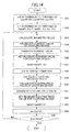
- FIG. 14 is a flowchart of a coupled analysis process performed by the coupled analysis simulation apparatus according to the first embodiment of the present invention.
- the coupled analysis process is executed by the coupled analysis control unit 221, the electromagnetic field analysis unit 222, the current calculation unit 223, the current transfer unit 224, the circuit analysis unit 225, the electric field calculation unit 226, and the electric field transfer unit 227 included in the coupled analysis processing unit 217.
- the times defined by the coupled analysis control unit 221 are input to the electromagnetic field analysis unit 222 and the electric field transfer unit 227.
- the electromagnetic field analysis unit 222 calculates the magnetic fields of all cells by using formula (4) (step S33).
- the circuit analysis unit 225 sets the current value received from the current transfer unit 224 as the current value of the coupling device 100 (step S36). Accordingly, the current value I n of the current source is updated to the current value of the coupling device 100 obtained by electromagnetic field analysis.
- the circuit analysis unit 225 uses the current value set in step S36 to solve the circuit equation (7) (step S38). Accordingly, the voltage value V of the coupling device 100 at the time t cs is obtained.
- the electromagnetic field analysis unit 222 calculates the electric fields of all cells by formula (5), with the use of the magnetic fields calculated in step S33 (step S39).
- the electric field calculation unit 226 obtains the electric field value E from the voltage value V of the coupling device 100 calculated in step S38 (step S40). This calculation is done with formula (8).
- the electric field transfer unit 227 transfers the electric field value E obtained in step S40 to the electromagnetic field analysis unit 222 (step S41).
- the electromagnetic field analysis unit 222 sets the electric field value received in step S41 as the electric field values of the cells in which the coupling device 100 is present (step S42). Accordingly, the electric field value of the coupling device 100 is updated to the value obtained by the circuit analysis.
- the circuit analysis unit 225 determines whether t cs ⁇ t max is satisfied (step S45). When the determination is affirmative, the process ends, and when the determination is negative, the flow returns to step S33.
- t max is the analysis time of electromagnetic field analysis, which is set in advance.
- the current values and the electric field values of the coupling device 100 are transferred between the electromagnetic field analysis unit 222 and the circuit analysis unit 225 to perform coupled analysis by performing electromagnetic field analysis and circuit analysis in coordination with each other.
- FIG. 15 indicates an example of data including electric field values and magnetic field values in cells in the analysis model used by the coupled analysis simulation apparatus according to the first embodiment of the present invention.
- FIG. 16 indicates data expressing current values obtained for the cells by the analysis model used in the coupled analysis simulation apparatus according to the first embodiment of the present invention.
- alphanumeric symbols are used for expressing the electric field values, magnetic field values, and current values; however, specific values obtained for the cells are used when the coupled analysis is actually performed.
- k is a natural number satisfying 0 ⁇ k ⁇ n.
- the data in FIG. 15 is obtained by the electromagnetic field analysis unit 222 for all of the cells in the analysis model, by alternately calculating a magnetic field and an electric field with the use of formula (4) and formula (5), respectively.
- the data of the current values I k indicated in FIG. 16 is obtained by the analysis result display processing unit 218, by performing contour integration on the magnetic field H (k+1/2) of each cell in FIG. 15 .
- the current values obtained for the cells are associated with the coordinates (X, Y, Z) of the analysis model as indicated in FIG. 16 and stored in the HDD 24.
- the current values stored in the HDD 24 are used as analysis results of the coupled analysis simulation apparatus according to the first embodiment of the present invention, when the analysis result display processing unit 218 causes the display screen 12A of the display 12 illustrated in FIG. 1 to display a return path to be reproduced in the power source layer or ground layer.
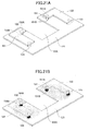
- FIG. 17B is a perspective view of the circuit of FIG. 17A , in which circuit the virtual conductive part 110 and the coupling devices 100A and 100B are virtually disposed instead of the electronic circuit module 120 and the terminals 120a and 120b illustrated in FIG. 17A .
- the dielectric layers are not illustrated as a matter of convenience.
- the ground layer 123 has a notch 123A, and therefore the ground layer 123 has a U-shape in a planar view.
- the wiring 121 and the wiring 122 are formed on the ground layer 123 via the dielectric layers that are not illustrated.
- the electronic circuit module 120 is connected in such a manner as to be positioned over the notch 123A of the ground layer 123.
- a resistor is illustrated as the electronic circuit module 120; however, the electronic circuit module 120 may be another electronic circuit module having multiple terminals, such as the LSI 36.
- the input port 124 connects the wiring 121 to the ground layer 123, and includes a current source for outputting a current of a predetermined current value.
- the output port 125 has a predetermined resistance value (typically 50 ( ⁇ )), and connects the wiring 122 to the ground layer 123.
- the electronic circuit module 120 and the terminals 120a and 120b are modeled, and the virtual conductive part 110 and coupling devices 100A and 100B are generated.
- the coupling device 100A is a virtual two-terminal device having one terminal 100Aa connected to a position where the terminal 120a of the electronic circuit module 120 is connected to the wiring 121.
- the coupling device 100B is a virtual two-terminal device having one terminal 100Ba connected to a position where the terminal 120b of the electronic circuit module 120 is connected to the wiring 122.
- the virtual conductive part 110 is defined so as to connect the other terminal 100Ab of the coupling device 100A to the other terminal 100Bb of the coupling device 100B. As a matter of convenience, the virtual conductive part 110 is illustrated as having a certain width in FIG. 17B . However, in the virtual conductive part data (see FIG. 8A ), the virtual conductive part 110 connecting the terminals 100Ab and 100Bb is defined as a line.
- the virtual conductive part data includes coordinates of four vertices.
- the virtual conductive part data expressing the virtual conductive part 110 illustrated in FIG. 17B includes coordinates of two points (the terminals 100Aa and 100Ba).
- FIG. 18 illustrates the return path reproduced by the coupled analysis simulation apparatus according to the first embodiment of the present invention.
- the return path is displayed as analysis results of the coupled analysis simulation apparatus according to the first embodiment, on the display screen 12A of the display 12 illustrated in FIG. 1 , by the analysis result display processing unit 218 (see FIG. 6 ).
- the return path is displayed as dots representing the distribution of current values indicated in FIG. 16 , on the surface of the ground layer 123. The higher the density of the dots, the higher the current values. The lower the density of the dots, the lower the current values.
- the virtual conductive part 110, the wiring 121, the wiring 122, the input port 124, and the output port 125 are illustrated with dotted lines so that the return path is clearly viewable.
- the return path illustrated in FIG. 18 is formed by reproducing a current pathway of signals on the surface of the ground layer 123. Specifically, the signals are input to the wiring 121 from the input port 124 illustrated in FIG. 17B , transmitted through the electronic circuit module 120, the wiring 122, the output port 125, and the ground layer 123, and are returned to the input port 124.
- the return path is accurately reproduced on the surface of the ground layer 123 by the coupled analysis simulation apparatus according to the first embodiment, starting from the output port 125, extending along the wiring 122, the notch 123A, and the wiring 121, and returning to the input port 124.
- FIC. 19A is a perspective view of a part of a circuit on which electronic circuit modules are mounted.
- FIG. 19B is a perspective view of the circuit of FIG. 19A , in which circuit virtual conductive parts and coupling devices are disposed.
- the circuit illustrated in FIG. 19A includes electronic circuit modules 120A through 120C, wirings 121A through 121C and 122A through 122C, a ground layer 123, input ports 124A through 124C, and output ports 125A through 125C.
- the input ports 124A through 124C respectively connect the wirings 121A through 121C to the ground layer 123, and include current sources that output currents of a predetermined current value.
- the output ports 125A through 125C have a predetermined resistance value (typically 50 ( ⁇ )), and respectively connect the wirings 122A through 122C to the ground layer 123.
- the electronic circuit modules 120A through 120C are respectively connected to the wirings 121A through 121C and 122A through 122C via terminals 120Aa through 120Ca and 120Ab through 120Cb.
- Dielectric layers of the printed circuit board are provided between the electronic circuit modules 120A through 120C, the wirings 121A through 121C and 122A through 122C, and the ground layer 123; however, the dielectric layers are not illustrated as a matter of convenience.
- Signals that are input from the input port 124B to the wiring 121B are transmitted through the electronic circuit module 120B, the wiring 122B, and the output port 125B, and returned to the input port 124B along the wiring 122B, the electronic circuit module 120B, and the wiring 121B on the ground layer 123.
- FIG. 19B illustrates virtual conductive parts 110A through 110C and coupling devices 108A through 108C and 109A through 109C, which are generated by modeling the electronic circuit modules 120A through 120C and the terminals 120Aa through 120Ca and 120Ab through 120Cb illustrated in FIG. 19A .
- the coupling device 108A is a virtual connection part having one terminal 108Aa connected to a position where the terminal 120Aa of the electronic circuit module 120A is connected to the wiring 121A in FIG. 19A .
- the coupling device 108B is a virtual connection part having one terminal 108Ba connected to a position where the terminal 120Ba of the electronic circuit module 120B is connected to the wiring 121B in FIG. 19A .
- the coupling device 108C is a virtual connection part having one terminal 108Ca connected to a position where the terminal 120Ca of the electronic circuit module 120C is connected to the wiring 121C in FIG. 19A .
- the coupling device 109A is a virtual connection part having one terminal 109Aa connected to a position where the terminal 120Ab of the electronic circuit module 120A is connected to the wiring 122A in FIG. 19A .
- the coupling device 109B is a virtual connection part having one terminal 109Ba connected to a position where the terminal 120Bb of the electronic circuit module 120B is connected to the wiring 122B in FIG. 19A .
- the coupling device 109C is a virtual connection part having one terminal 109Ca connected to a position where the terminal 120Cb of the electronic circuit module 120C is connected to the wiring 122C in FIG. 19A .
- the actual heights of the electronic circuit modules 120A through 120C from the wirings 121A through 121C and 122A through 122C are set as the heights of the coupling devices 108A through 108C and 109A through 109C.
- the positions and heights where the coupling devices 108A through 108C and 109A through 109C are connected to the wirings 121A through 121C and 122A through 122C are determined according to the coupling device data (see FIG. 8B ).
- Each virtual conductive part data item expressing one of the virtual conductive parts 110A through 110C illustrated in FIG. 19B includes coordinates of two points (the terminals 108Aa through 108Ca and 109Aa through 109Ca).
- FIG. 20 illustrates the return path reproduced on the circuit illustrated in FIG. 19B by the coupled analysis simulation apparatus according to the first embodiment of the present invention.
- the return path is displayed as analysis results of the coupled analysis simulation apparatus according to the first embodiment, on the display screen 12A of the display 12 illustrated in FIG. 1 , by the analysis result display processing unit 218 (see FIG. 6 ) .
- the return path illustrated in FIG. 20 is reproduced on the surface of the ground layer 123, when signals are input to the electronic circuit modules 120A and 120C illustrated in FIG. 19A , but not input to the electronic circuit module 120B.
- the return path is indicated by dots in FIG. 20 .
- FIG. 21A is a perspective view of a circuit with coupling devices defined by a conventional coupled analysis simulation apparatus.
- FIG. 21B illustrates a return path reproduced on the circuit illustrated in FIG. 21A by the conventional coupled analysis simulation apparatus.
- the return path is indicated by dots in FIG. 21B .
- elements except for the ground layer 123 are illustrated with dotted lines so that the return path is clearly viewable.
- the conventional coupling devices 150 and 151 illustrated in FIG. 21A are defined as conventional coupling devices of the terminals 120a and 120b of the electronic circuit module 120 illustrated in FIG. 17A .
- the conventional coupling devices 150 and 151 respectively include terminals 150A and 151A that are connected to the wiring 121 and the wiring 122, as well as terminals 150B and 151B that are connected to the nearest ground layer 123.
- FIG. 21B illustrates a return path that is reproduced by the conventional coupled analysis simulation apparatus in which conventional coupling devices 150 and 151 are virtually connected to a circuit.
- the return path does not diverge around the notch 123A; the return path is separated on either side of the notch 123A. That is to say, the return path is reproduced at two separate positions on the ground layer 123, i.e., the position under the wiring 121 and the position under the wiring 122.
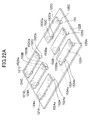
- FIG. 22A is a perspective view of a circuit with coupling devices defined by a conventional coupled analysis simulation apparatus.
- FIG. 22B illustrates a return path reproduced on the circuit illustrated in FIG. 22A by the conventional coupled analysis simulation apparatus.
- the return path is indicated by dots in FIG. 22B .
- elements except for the ground layer 123 are illustrated with dotted lines so that the return path is clearly viewable.
- the conventional coupling devices 152A through 152C and 153A through 153C illustrated in FIG. 22A are defined as conventional coupling devices of the terminals 120Aa through 120Ca and 120Ab through 120Cb of the electronic circuit modules 120A through 120C illustrated in FIG. 19A .
- the conventional coupling devices 152A, 152B, and 152C respectively include terminals 152Aa, 152Ba, and 152Ca that are connected to the wirings 121A, 121B, and 121C, as well as terminals 152Ab, 152Bb, and 152Cb that are connected to the nearest ground layer 123.
- the return path illustrated in FIG. 22B is reproduced on the surface of the ground layer 123 by a conventional coupled analysis simulation apparatus when signals are input to the electronic circuit modules 120A and 120C illustrated in FIG. 19A but not input to the electronic circuit module 120B illustrated in FIG. 19A .
- the return path reproduced by a conventional coupled analysis simulation apparatus is broken in between the wiring 121A and the wiring 122A, and is also broken in between the wiring 121C and the wiring 122C, on the surface of the ground layer 123.
- the coupled analysis simulation apparatus uses the virtual conductive parts 110 and the coupling devices 100 that are generated by modeling the electronic circuit modules and terminals. Therefore, the coupled analysis is performed on the electronic circuit modules in a state that is similar to the actual state in which the electronic circuit modules are actually connected to the conductive layers 35.
- the electromagnetic field analysis involves processes of calculating the electric fields and magnetic fields of cells in the analysis model including the virtual conductive parts 110 and the coupling devices 100.
- the electric fields and magnetic fields of the cells where the electronic circuit modules are actually positioned it is possible to obtain, with high precision, the current value of the coupling device 100 to be transferred to (applied to) the circuit analysis process.
- connection process is completed simply by connecting all of the coupling devices 100 to the virtual conductive parts 110. Accordingly, the modeling process is very simple.
- the connection process is completed simply by connecting all of the coupling devices 100 to the virtual conductive parts 110, and therefore the connection process of the coupling devices 100 is very simple. Accordingly, the return path is accurately reproduced.
- the virtual conductive part 110 has a linear shape or a planar shape that does not have a thickness; however, the virtual conductive part 110 may be defined as having a certain thickness.
- FIG. 23 illustrates the connection of a virtual conductive part and coupling devices that are defined by a coupled analysis simulation apparatus according to a second embodiment of the present invention.
- each of the electronic circuit modules is modeled to generate separate virtual conductive parts.
- a common virtual conductive part is generated for plural electronic circuit modules, which is the point different from that of the first embodiment.
- the following description mainly concerns different aspects from the first embodiment, and elements corresponding to the coupled analysis simulation apparatus according to the first embodiment are denoted by the same reference numerals and are not further described.
- Coupling devices 201 through 207 according to the second embodiment illustrated in FIG. 23 are embodiments of virtual connection parts generated by modeling the bumps 38A through 38E and the terminals 37A and 37B illustrated in FIG. 5A .
- the virtual conductive part 210 is generated as a common virtual conductive part corresponding to the LSI 36 and the bypass capacitor 37, by modeling the LSI 36 and the bypass capacitor 37 illustrated in FIG. 5A .
- the virtual conductive part 210 is defined as a perfect conductor.
- the virtual conductive part 210 corresponding to two electronic circuit modules is generated as a common virtual conductive part corresponding to plural electronic circuit modules.
- the common virtual conductive part may correspond to any number of electronic circuit modules.
- a common virtual conductive part may be generated for all electronic circuit modules mounted on one side of the printed circuit board 34, or a common virtual conductive part may be generated for some of the electronic circuit modules.
- the printed circuit board 34 may be divided into several regions, and a common virtual conductive part may be generated for each of the regions.
- the coupling devices 201 through 207 and the virtual conductive part 210 are defined as perfect conductors; however, the coupling devices 201 through 207 and the virtual conductive part 210 may be defined as conductors other than perfect conductors.
- the coupling devices 201 through 207 may be referred to as a coupling device 200, when the coupling devices 201 through 207 are not particularly distinguished from one another.
- the process illustrated in FIG. 24 is applied to a case of generating the planar virtual conductive part 210 that is specified by four vertices. Coordinates of the four vertices are (Xmin, Ymin), (Xmin, Ymax), (Xmax, Ymin), and (Xmax, Ymax).
- the virtual conductive part generating unit 214 reads the CAD data (see FIG. 4C ) corresponding to the electronic circuit module having the lowest identifier number among the electronic circuit modules included in the analysis conditions (step S50).
- the virtual conductive part generating unit 214 reads the layer number of the conductive layer 35 on which the electronic circuit module (CAD data) read in step S50 is mounted (step S51). For example, when the electronic circuit module of the corresponding identifier (No.) in the CAD data indicated in FIG. 4C has a layer number of 1, the virtual conductive part generating unit 214 recognizes that this electronic circuit module is mounted on the topmost layer. When the electronic circuit module of the corresponding identifier (No.) in the CAD data indicated in FIG. 4C has a layer number of 4, the virtual conductive part generating unit 214 recognizes that this electronic circuit module is mounted on the bottommost layer.
- the virtual conductive part generating unit 214 specifies the X, Y coordinates of the terminal having the smallest terminal number among the terminals of the electronic circuit module having the smallest identifier indicated in the analysis conditions, as the initial X, Y coordinates expressing the position of the virtual conductive part 210 (step S52).
- the virtual conductive part generating unit 214 reads, from the CAD data, the coordinates (Xti, Yti) of the terminal (step S53). The process flow repeatedly returns to step S53 (after step S64) to sequentially read the coordinates of the terminals in an ascending order of terminal numbers.
- the virtual conductive part generating unit 214 reads, from the CAD data, the coordinates (Xti, Yti) of the terminal having the next smallest terminal number among the terminal numbers relevant to the electronic circuit module read in step S50.
- step S52 when the virtual conductive part generating unit 214 has read, in step S52, the coordinates (Xt1, Yt1) of terminal 1 of the electronic circuit module having an identifier (No.) 1 indicated in FIG. 4C , the virtual conductive part generating unit 214 reads, in step S53, coordinates (Xt2, Yt2) of terminal 2.
- the virtual conductive part generating unit 214 determines whether Xmax ⁇ Xti is satisfied with respect to the X coordinate (Xti) of the coordinates (Xti, Yti) of the terminal read in step S53 (step S54).
- step S54 When the virtual conductive part generating unit 214 determines that Xmax ⁇ Xti is satisfied in step S54 (Yes in steps S54), the virtual conductive part generating unit 214 sets Xti as Xmax (step S55). Accordingly, the value of Xmax is set to an even larger value Xti.
- step S54 determines whether Xmax ⁇ Xti is not satisfied in step S54 (No in steps S54), or when the process of step S55 has ended.
- the virtual conductive part generating unit 214 determines whether Ymax ⁇ Yti is satisfied with respect to the Y coordinate (Yti) of the coordinates (Xti, Yti) (step S56).
- step S56 When the virtual conductive part generating unit 214 determines that Ymax ⁇ Yti is satisfied in step S56 (Yes in step S56), the virtual conductive part generating unit 214 sets Yti as Ymax (step S57). Accordingly, the value of Ymax is set to an even larger value Yti.
- step S58 determines whether Xmin > Xti is satisfied with respect to the X coordinate (Xti) of the coordinates (Xti, Yti) (step S58).
- step S58 When the virtual conductive part generating unit 214 determines that Xmin > Xti is satisfied in step S58 (Yes in step S58), the virtual conductive part generating unit 214 sets Xti as Xmin (step S59). Accordingly, the value of Xmin is updated to an even smaller value Xti.
- step S58 determines that Xmin > Xti is not satisfied in step S58 (No in step S58), or when the process of step S59 has ended.
- the virtual conductive part generating unit 214 determines whether Ymin > Yti is satisfied with respect to the Y coordinate (Yti) of the coordinates (Xti, Yti) (step S60).
- step S60 When the virtual conductive part generating unit 214 determines that Ymin > Yti is satisfied in step S60 (Yes in step S60), the virtual conductive part generating unit 214 sets Yti as Ymin (step S61). Accordingly, the value of Ymin is updated to an even smaller value Yti.
- step S62 determines whether the currently processed terminal is the last terminal.
- the process of step S62 is for determining whether steps S53 through S61 have been completed for all of the terminals specified in the analysis conditions.
- the virtual conductive part generating unit 214 determines whether the currently processed terminal is the last terminal based on the terminal number of the terminal of the electronic circuit module included in the analysis results.
- step S63 the virtual conductive part generating unit 214 determines, in step S63, that the currently processed electronic circuit module is not the last electronic circuit module (No in step S63)
- the virtual conductive part generating unit 214 reads the CAD data of the next electronic circuit module in the analysis conditions (step S64).
- step S64 the CAD data of the electronic circuit module having the next smallest identifier is read.
- step S64 ends, the virtual conductive part generating unit 214 returns to step S53.
- the process flow repeatedly returns to step S53 (after step S64) to sequentially read the coordinates of the terminals in an ascending order of terminal numbers with respect to the electronic circuit module read in step S64.
- step S63 determines, in step S63, that the currently processed electronic circuit module is the last electronic circuit module (Yes in step S63)
- the virtual conductive part generating unit 214 determines the values of Xmax, Xmin, Ymax, and Ymin (step S65). Accordingly, the four vertices of the virtual conductive part 210 are determined as (Xmin, Ymin), (Xmin, Ymax), (Xmax, Ymin), and (Xmax, Ymax).
- the virtual conductive part generating unit 214 reads the height (h) of the virtual conductive part 210 included in the analysis conditions (step S67). This step is performed to set a value created by the analysis condition creating unit 213 in advance as the height between the virtual conductive part 210 and the front surface (or back surface) of the printed circuit board 34.
- each coupling device 200 is defined to be at a position of one of the terminals included in the analysis conditions.
- the coupling device 200 is a virtual connection part that virtually connects the conductive layers 35 to the virtual conductive part 210.
- the positions of both terminals of the coupling device 200 which is a two-terminal device, are identified. This identification is done by associating the X, Y coordinates of the terminal included in the analysis conditions among the terminals included in the CAD data indicated in FIG. 4C , with the layer number and height of the virtual conductive part 210 registered in step S68.
- the coupling device 200 is defined by associating the identifier of the coupling device 200, X, Y coordinates, the layer number, and the height.
- the height of the coupling device 200 is expressed by +h or -h; +h is the height between the coupling device 200 and the topmost conductive layer 35, and -h is the height between the coupling device 200 and the bottommost conductive layer 35.
- the layer number expresses whether the position where the coupling device 200 is defined is on the topmost layer or the bottommost layer.
- the virtual connection part generating unit 215 determines whether the terminal defining the coupling device 200 processed in step S69 is the last terminal (step S70).
- the terminals included in the analysis conditions are selected one by one starting from the smallest terminal number to define each coupling device, and the selected terminal is processed in step S69. Therefore, step S69 is repeatedly performed until it is determined in step S70 that the processed terminal is the last terminal.
- step S69 multiple coupling device data items are created, in which the identifier of the coupling device 200, the X, Y coordinates, and the height are associated with each other.
- the virtual connection part generating unit 215 creates a net list of the coupling devices 200 (step S71).
- step S71 When the virtual connection part generating unit 215 has created a net list in step S71, the series of steps for defining the virtual conductive part 210 and the coupling devices 200 are ended.
- the coupled analysis simulation apparatus uses the virtual conductive part 110 and the coupling devices 200 that are generated by modeling the electronic circuit modules and terminals. Therefore, the coupled analysis is performed on the electronic circuit modules in a state that is similar to the actual state in which the electronic circuit modules are actually connected to the conductive layers 35.
- the electromagnetic field analysis involves processes of calculating the electric fields and magnetic fields of cells in the analysis model including the virtual conductive part 210 and the coupling devices 100.
- the electric fields and magnetic fields of the cells where the electronic circuit modules are actually positioned.
- the virtual conductive part 210 that is common to plural electronic circuit modules is generated. Therefore, in the second embodiment, the process for generating the virtual conductive part 210 is further simplified than that of the first embodiment. Accordingly, in the second embodiment, it is possible perform coupled analysis with fewer calculation steps compared to the first embodiment.
- connection process is completed simply by connecting all of the coupling devices 200 to the virtual conductive part 210. Accordingly, the process of modeling the electronic circuit module and terminals is very simple.
- the connection process is completed simply by connecting all of the coupling devices 200 to the virtual conductive part 210, and therefore the connection process of the coupling devices 200 is very simple. Accordingly, the return path is accurately reproduced.
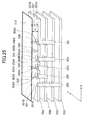
- FIG. 25 illustrates the connection of a virtual conductive part and coupling devices that are defined by a coupled analysis simulation apparatus according to a third embodiment of the present invention.
- the third embodiment is different from the first embodiment in that a virtual conductive part 310 is generated, which has the same size as the printed circuit board 34 in a planar view. All of the coupling devices, which are generated by modeling the terminals of all of the electronic circuit modules in the analysis conditions, are connected to the virtual conductive part 310.
- Coupling devices 301 through 307 according to the third embodiment illustrated in FIG. 25 are embodiments of virtual connection parts generated by modeling the bumps 38A through 38E and the terminals 37A and 37B illustrated in FIG. 5A .
- the coupling devices 301 through 307 include terminals 301A through 307A that are connected to the same conductive layers as those to which the terminals have been connected before being modeled (any of conductive layers 35A through 35D). Furthermore, the coupling devices 301 through 307 include terminals 301B through 307B that are connected to the virtual conductive part 310.
- the coupled analysis simulation apparatus according to the third embodiment uses the coupling devices 301 through 307 that are two-terminal devices to connect the conductive layers 35A through 35D to the virtual conductive part 310.
- the coupling devices 301 through 307 are defined as perfect conductors. In this example, perfect conductors have an electric resistance of zero.
- the virtual conductive part 310 is set as a plane having the same size as the printed circuit board 34 in a planar view.
- FIG. 25 illustrates only the coupling devices 301 through 307 that have been generated by modeling the bumps 38A through 38E of the LSI 36 and the terminals 37A and 37B of the bypass capacitor 37 (see FIG. 5A ). However, actually terminals of all electronic circuit module specified in the analysis conditions are modeled, and therefore coupling devices other than the coupling devices 301 through 307 may be generated as well.
- the virtual conductive part 310 has the same size as the printed circuit board 34 in a planar view, and is therefore connected to all of the coupling devices defined on either the topmost layer or the bottommost layer of the printed circuit board 34.
- the coupling devices 301 through 307 and the virtual conductive part 310 are defined as perfect conductors; however, the coupling devices 301 through 307 and the virtual conductive part 310 may be defined as conductors other than perfect conductors.
- the coupling devices 301 through 307 may be referred to as coupling devices 300, when the coupling devices 301 through 307 are not particularly distinguished from one another.
- the printed circuit board 34 is a rectangle in a planar view. Therefore, the data expressing the size of the printed circuit board indicates coordinates of four vertices of the printed circuit board 34 in an X, Y coordinate plane, as indicated in FIG. 26 .
- alphanumeric symbols are used for expressing the coordinates of the four vertices of the printed circuit board 34; however, when the coupled analysis is actually performed, specific values expressing X, Y coordinates corresponding to the positions of the four vertices of the printed circuit board 34 are used.
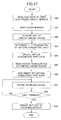
- FIG. 27 is a flowchart of a process for generating a virtual conductive part and coupling devices in the coupled analysis simulation apparatus according to the third embodiment of the present invention.
- the process illustrated in FIG. 27 is what the main control unit 211 inside the CPU 21 causes the virtual conductive part generating unit 214 and the virtual connection part generating unit 215 to execute. This process is executed according to analysis conditions created by the analysis condition creating unit 213.
- the virtual conductive part generating unit 214 reads the CAD data (see FIG. 4C ) corresponding to the electronic Circuit module having the lowest identifier number among the electronic circuit modules included in the analysis conditions (step S80).
- the layer number of the LSI 36 is read, so that the virtual conductive part generating unit 214 recognizes whether the LSI 36 is mounted on the conductive layer 35A that is the topmost layer or the conductive layer 35D that is the bottommost layer.
- the virtual conductive part generating unit 214 reads the size of the printed circuit board 34 (step S82).
- the printed circuit board 34 is a rectangle in a planar view. Therefore, the virtual conductive part generating unit 214 reads the X, Y coordinates of four vertices from the data indicated in FIG. 26 .
- the virtual conductive part generating unit 214 creates virtual conductive part data, by associating the coordinates of the four vertices determined in step S83 with the identifier of the virtual conductive part 310 (step S84).
- the virtual conductive part data is obtained by associating the identifier, the X, Y coordinate values of the vertices, and the height of the virtual conductive part 310, as in the CAD data.
- the virtual conductive part generating unit 214 reads the height (h) of the electronic circuit module 310 included in the analysis conditions (step S85). This step is performed to set a value created by the analysis condition creating unit 213 in advance as the height of the virtual conductive part 310 from the front surface (or back surface) of the printed circuit board 34.
- the virtual conductive part generating unit 214 adds, to the virtual conductive part data, the layer number read in step S81 and the height of the virtual conductive part 310 read in step S85 (step S86).
- the virtual conductive part generating unit 214 has recognized that the corresponding conductive layer 35 is the topmost layer in step S81, the height of the virtual conductive part 210 is registered as +h.
- the virtual conductive part generating unit 214 has recognized that the corresponding conductive layer 35 is the bottommost layer in step S81, the height of the virtual conductive part 210 is registered as -h.
- the layer number is registered as data for expressing the layer on which the electronic circuit module is mounted.
- each coupling device 300 is defined to be at a position of one of the terminals included in the analysis conditions.
- the coupling device 300 is a virtual connection part that virtually connects the conductive layers 35 to the virtual conductive part 310.
- the positions of both terminals of the coupling device 300 which is a two-terminal device, are identified. This identification is done by associating the X, Y coordinates of the terminal included in the analysis conditions among the terminals included in the CAD data indicated in FIG. 4C , with the layer number and height of the virtual conductive part 310 registered in step S86.
- the coupling device 300 is defined by associating the identifier of the coupling device 300, X, Y coordinates, the layer number, and the height.
- the virtual connection part generating unit 215 sequentially reads the X, Y, coordinates of the terminals included in the analysis conditions one by one starting from the smallest terminal number.
- the virtual connection part generating unit 215 associates the X, Y coordinates of the corresponding terminal with the layer number and the height of the virtual conductive part 310 registered in step S86, and gives an identifier to the coupling device 300.
- the virtual connection part generating unit 215 determines whether the terminal defining the coupling device 300 processed in step S87 is the last terminal (step S88).
- the terminals included in the analysis conditions are selected one by one starting from the smallest terminal number to define each coupling device, and the selected terminal is processed in step S87. Therefore, step S87 is repeatedly performed until it is determined in step S88 that the processed terminal is the last terminal.
- step S87 multiple coupling device data items are created, in which the identifier of the coupling device 300, the X, Y coordinates, and the height are associated with each other.
- the virtual connection part generating unit 215 creates a net list of the coupling devices 300 (step S89).
- step S89 When the virtual connection part generating unit 215 has created a net list in step S89, the series of steps for defining the virtual conductive part 310 and the coupling devices 300 is ended.
- FIG. 28B is a perspective view of the circuit of FIG. 28A , in which circuit virtual conductive parts and coupling devices are disposed.
- virtual coupling devices 308A through 108C and 309A through 309C are disposed, and the virtual conductive part 310 is disposed instead of the electronic circuit modules 120A through 120C illustrated in FIG. 28A .
- the virtual coupling devices 308A through 108C and 309A through 309C are basically the same as the coupling devices 108A through 108C and 109A through 109C illustrated in FIG. 19B in the first embodiment.
- the virtual coupling devices 308A through 308C and 309A through 309C include terminals 308Aa through 308Ca and 309Aa through 309Ca that are connected to the wirings 121A through 121C and 122A through 122C, and terminals 308Ab through 308Cb and 309Ab through 309Cb that are connected to the virtual conductive part 310.
- FIG. 28B illustrates only the coupling devices 308A through 308C and 309A through 309C; however, there may be coupling devices other than the coupling devices 308A through 308C and 309A through 309C when more terminals of electronic circuit modules are specified in the analysis conditions. All coupling devices generated according to the analysis conditions are connected to the virtual conductive part 310.
- FIG. 29 illustrates a return path reproduced on the circuit illustrated in FIG. 28B by the coupled analysis simulation apparatus according to the third embodiment of the present invention.
- the return path is displayed as analysis results of the coupled analysis simulation apparatus according to the third embodiment, on the display screen 12A of the display 12 illustrated in FIG. 1 , by the analysis result display processing unit 218 (see FIG. 6 ).
- the return path illustrated in FIG. 29 is reproduced on the surface of the ground layer 123, when signals are input to the electronic circuit modules 120A and 120C illustrated in FIG. 28A , but not input to the electronic circuit module 120B.
- the return path is indicated by dots in FIG. 29 .
- elements except for the ground layer 123 are illustrated with dotted lines so that the return path is clearly viewable.
- the return path extends on the surface of the ground layer 123, along the wiring 121A, the virtual conductive part 310, the wiring 122A, the wiring 121C, the virtual conductive part 310, and the wiring 122C.
- the return path illustrated in FIG. 29 is different from that of the coupled analysis simulation apparatus according to the first embodiment in that a slight current expressed by dots of low density is flowing between the wirings 121A and 121C and between the wirings 122A through 122C; however, the return path of FIG. 29 is accurately reproduced on the circuit illustrated in FIG. 29 .
- the coupled analysis simulation apparatus uses the virtual conductive part 310 and the coupling devices 300 that are generated by modeling the electronic circuit modules and terminals. Therefore, the coupled analysis is performed on the electronic circuit modules in a state that is similar to the actual state in which the electronic circuit modules are actually connected to the conductive layers 35.
- the electromagnetic field analysis involves processes of calculating the electric fields and magnetic fields of cells in the analysis model including the virtual conductive part 310 and the coupling devices 300.
- the electric fields and magnetic fields of the cells where the electronic circuit modules are actually positioned.
- the virtual conductive part 310 having the same size as the printed circuit board 34 in a planar view is generated as a virtual conductive part common to all electronic circuit modules mounted on the printed circuit board 34. Therefore, in the third embodiment, the process for generating the virtual conductive part 310 is further simplified than that of the first and second embodiments. Accordingly, in the third embodiment, it is possible perform coupled analysis with fewer calculation steps compared to the first and second embodiments.
- connection process is completed simply by connecting all of the coupling devices 300 to the virtual conductive part 310. Accordingly, the process of modeling the electronic circuit module and terminals is very simple.
- the printed circuit board 34 has a rectangular shape in a planar view; however, when the printed circuit board 34 is not a rectangle, the size of the virtual conductive part 310 may be defined so as to cover the entire printed circuit board 34 in a planar view.
- the FDTD method is used for electromagnetic field analysis; however, the electromagnetic field analysis is not limited to the FDTD method.
- the electromagnetic field analysis may be performed by any calculation method for deriving the variation in the time-domain of the electromagnetic field, such as a moment method and a TLM method.
- a coupled analysis simulation apparatus a coupled analysis simulation method, and a computer-readable recording medium are provided, with which electronic circuit modules and connection parts are easily modeled and a return path is accurately reproduced.
Landscapes
- Engineering & Computer Science (AREA)
- Computer Hardware Design (AREA)
- Physics & Mathematics (AREA)
- Theoretical Computer Science (AREA)
- Evolutionary Computation (AREA)
- Geometry (AREA)
- General Engineering & Computer Science (AREA)
- General Physics & Mathematics (AREA)
- Microelectronics & Electronic Packaging (AREA)
- Design And Manufacture Of Integrated Circuits (AREA)
Applications Claiming Priority (1)
| Application Number | Priority Date | Filing Date | Title |
|---|---|---|---|
| JP2009233251A JP4952763B2 (ja) | 2009-10-07 | 2009-10-07 | 連携解析シミュレーション装置、連携解析シミュレーション方法、及び連携解析シミュレーションプログラム |
Publications (1)
| Publication Number | Publication Date |
|---|---|
| EP2378446A2 true EP2378446A2 (de) | 2011-10-19 |
Family
ID=43402221
Family Applications (1)
| Application Number | Title | Priority Date | Filing Date |
|---|---|---|---|
| EP10178437A Withdrawn EP2378446A2 (de) | 2009-10-07 | 2010-09-22 | Gekoppelte Analysesimulationsvorrichtung und gekoppeltes Analysesimulationsverfahren |
Country Status (3)
| Country | Link |
|---|---|
| US (1) | US8768677B2 (de) |
| EP (1) | EP2378446A2 (de) |
| JP (1) | JP4952763B2 (de) |
Families Citing this family (17)
| Publication number | Priority date | Publication date | Assignee | Title |
|---|---|---|---|---|
| US8285407B2 (en) * | 2007-10-25 | 2012-10-09 | The Boeing Company | Method and apparatus for composite part data extraction |
| US8442804B2 (en) * | 2007-10-25 | 2013-05-14 | The Boeing Company | Method and apparatus for composite part data extraction |
| US8620627B2 (en) | 2009-10-13 | 2013-12-31 | The Boeing Company | Composite information display for a part |
| US8652606B2 (en) | 2010-08-17 | 2014-02-18 | The Boeing Company | Composite structures having composite-to-metal joints and method for making the same |
| US9522512B2 (en) | 2010-08-17 | 2016-12-20 | The Boeing Company | Methods for making composite structures having composite-to-metal joints |
| US8993084B2 (en) | 2010-08-17 | 2015-03-31 | The Boeing Company | Multi-layer metallic structure and composite-to-metal joint methods |
| JP5974792B2 (ja) * | 2012-10-02 | 2016-08-23 | 株式会社ソシオネクスト | 電磁界回路連携解析プログラム、電磁界回路連携解析装置及び電磁界回路連携解析方法 |
| JP6164096B2 (ja) * | 2014-01-17 | 2017-07-19 | 株式会社ソシオネクスト | 解析支援装置、および解析支援方法 |
| US10380292B1 (en) * | 2016-04-08 | 2019-08-13 | Cadence Design Systems, Inc. | Systems and methods for finite difference time domain simulation of an electronic design |
| RU2715794C1 (ru) * | 2019-07-25 | 2020-03-03 | Денис Александрович Давыдов | Способ симуляции электрической схемы, система для его осуществления и симулирующий компонент |
| US11806948B2 (en) | 2019-12-12 | 2023-11-07 | The Boeing Company | Method of forming flyaway stringer end caps |
| US11718047B2 (en) | 2019-12-12 | 2023-08-08 | The Boeing Company | Flyaway stringer end caps |
| US11416657B2 (en) * | 2020-03-20 | 2022-08-16 | Sonnet Software, Inc. | Method for simulating vertically oriented current in a structure |
| CN112115553B (zh) * | 2020-09-17 | 2023-04-14 | 东风柳州汽车有限公司 | 车辆电磁兼容仿真方法、设备、存储介质及装置 |
| JP7575839B2 (ja) * | 2021-02-02 | 2024-10-30 | パナソニックオートモーティブシステムズ株式会社 | 情報処理装置、情報処理方法、及び、プログラム |
| GB2618576B (en) * | 2022-05-11 | 2025-04-09 | Monumo Ltd | Virtual current representation of magnetic fields for electric motor design |
| CN116436546B (zh) * | 2023-04-21 | 2026-03-27 | 重庆邮电大学 | Pcb电磁泄漏作用传输线的电磁耦合时域分析方法和系统 |
Citations (4)
| Publication number | Priority date | Publication date | Assignee | Title |
|---|---|---|---|---|
| JPH11153634A (ja) | 1997-11-19 | 1999-06-08 | Fujitsu Ltd | シミュレーション装置及びシミュレーションプログラムを記録したコンピュータ読み取り可能な記録媒体 |
| JP2004054642A (ja) | 2002-07-19 | 2004-02-19 | Sony Corp | 回路解析システム及びその解析方法 |
| WO2004109560A1 (ja) | 2003-06-05 | 2004-12-16 | Fujitsu Limited | 回路解析と電磁波解析との連携による電磁界強度算出装置および算出方法 |
| JP2008217327A (ja) | 2007-03-02 | 2008-09-18 | Sharp Corp | 電磁界回路連携解析装置、電磁界回路連携解析プログラム、電磁界回路連携解析プログラムを格納した記録媒体および電磁界回路連携解析方法 |
Family Cites Families (4)
| Publication number | Priority date | Publication date | Assignee | Title |
|---|---|---|---|---|
| JP3838328B2 (ja) * | 2000-02-28 | 2006-10-25 | 日本電気株式会社 | 設計支援装置および設計支援装置に含まれるコンピュータに実行させるためのプログラムを記録したコンピュータ読みとり可能な記録媒体 |
| JP4684188B2 (ja) * | 2006-08-30 | 2011-05-18 | シャープ株式会社 | 回路モデル作成プログラム、回路モデル作成プログラムを格納したコンピュータ読み取り可能な記録媒体および回路モデル作成装置 |
| JP2008083997A (ja) * | 2006-09-27 | 2008-04-10 | Fujitsu Ltd | 回路装置設計装置、回路装置設計方法及び回路装置設計プログラム |
| JP4644740B2 (ja) * | 2006-12-28 | 2011-03-02 | 富士通株式会社 | シミュレーションシステム、およびシミュレーションプログラム |
-
2009
- 2009-10-07 JP JP2009233251A patent/JP4952763B2/ja not_active Expired - Fee Related
-
2010
- 2010-09-22 EP EP10178437A patent/EP2378446A2/de not_active Withdrawn
- 2010-10-06 US US12/899,135 patent/US8768677B2/en not_active Expired - Fee Related
Patent Citations (4)
| Publication number | Priority date | Publication date | Assignee | Title |
|---|---|---|---|---|
| JPH11153634A (ja) | 1997-11-19 | 1999-06-08 | Fujitsu Ltd | シミュレーション装置及びシミュレーションプログラムを記録したコンピュータ読み取り可能な記録媒体 |
| JP2004054642A (ja) | 2002-07-19 | 2004-02-19 | Sony Corp | 回路解析システム及びその解析方法 |
| WO2004109560A1 (ja) | 2003-06-05 | 2004-12-16 | Fujitsu Limited | 回路解析と電磁波解析との連携による電磁界強度算出装置および算出方法 |
| JP2008217327A (ja) | 2007-03-02 | 2008-09-18 | Sharp Corp | 電磁界回路連携解析装置、電磁界回路連携解析プログラム、電磁界回路連携解析プログラムを格納した記録媒体および電磁界回路連携解析方法 |
Also Published As
| Publication number | Publication date |
|---|---|
| JP4952763B2 (ja) | 2012-06-13 |
| US20110082681A1 (en) | 2011-04-07 |
| JP2011081597A (ja) | 2011-04-21 |
| US8768677B2 (en) | 2014-07-01 |
Similar Documents
| Publication | Publication Date | Title |
|---|---|---|
| EP2378446A2 (de) | Gekoppelte Analysesimulationsvorrichtung und gekoppeltes Analysesimulationsverfahren | |
| US5566083A (en) | Method for analyzing voltage fluctuations in multilayered electronic packaging structures | |
| CN111488717B (zh) | 标准单元时序模型的抽取方法、装置、设备及存储介质 | |
| US20060173662A1 (en) | Electromagnetic field analysis apparatus, method and computer program | |
| US20090102470A1 (en) | Simulation method implemented by coupling electromagnetic field analysis method and circuit analysis method together, simulation apparatus, and computer-readable medium storing simulation program | |
| US7310595B2 (en) | Numerically modeling inductive circuit elements | |
| KR101139080B1 (ko) | 프린트 기판 시험 지원 장치, 프린트 기판 시험 지원 방법 및 프린트 기판 시험 지원 프로그램을 기록한 컴퓨터 판독 가능한 기록 매체 | |
| US7644381B2 (en) | Electromagnetic coupled basis functions for an electronic circuit | |
| JP2010262338A (ja) | 電磁流分布処理装置、電磁流分布処理方法、及び電磁流分布処理プログラム | |
| KR20110009634A (ko) | 배선 설계 지원 장치, 배선 설계 지원 방법, 및 배선 설계 지원 프로그램을 기록한 컴퓨터 판독가능한 기록 매체 | |
| Fan et al. | Modeling DC power-bus structures with vertical discontinuities using a circuit extraction approach based on a mixed-potential integral equation | |
| Shi et al. | Fast calculation method for crosstalk of high-density printed circuit board by using machine learning | |
| JP2009266219A (ja) | 回路基板の解析装置および解析方法 | |
| US7197446B2 (en) | Hierarchical method of power supply noise and signal integrity analysis | |
| CN120046285A (zh) | 一种直流压降计算方法、计算机设备及存储介质 | |
| US7962320B2 (en) | Method, apparatus and program for creating a power pin model of a semiconductor integrated circuit | |
| CN102651038B (zh) | 用于电力输送网络分析的方法和系统 | |
| Fukumoto et al. | A method of automatic placement that reduces electromagnetic radiation noise from digital printed circuit boards | |
| JP2009123132A (ja) | プリント基板設計支援装置、プリント基板設計支援方法およびプリント基板設計支援プログラム | |
| Kim et al. | An efficient methodology for extraction and simulation of transmission lines for application specific electronic modules | |
| Coperich et al. | Rigorous modeling of the frequency dependence of ohmic losses in high-speed electrical interconnections | |
| JP4684188B2 (ja) | 回路モデル作成プログラム、回路モデル作成プログラムを格納したコンピュータ読み取り可能な記録媒体および回路モデル作成装置 | |
| JP4843091B2 (ja) | パワーインテグリティ解析装置及び方法並びにプログラム | |
| CN102651039B (zh) | 用于电力输送网络分析的方法和系统 | |
| US8204722B2 (en) | Simulation apparatus, simulation method, and simulation program |
Legal Events
| Date | Code | Title | Description |
|---|---|---|---|
| AK | Designated contracting states |
Kind code of ref document: A2 Designated state(s): AL AT BE BG CH CY CZ DE DK EE ES FI FR GB GR HR HU IE IS IT LI LT LU LV MC MK MT NL NO PL PT RO SE SI SK SM TR |
|
| AX | Request for extension of the european patent |
Extension state: BA ME RS |
|
| PUAI | Public reference made under article 153(3) epc to a published international application that has entered the european phase |
Free format text: ORIGINAL CODE: 0009012 |
|
| STAA | Information on the status of an ep patent application or granted ep patent |
Free format text: STATUS: THE APPLICATION HAS BEEN WITHDRAWN |
|
| 18W | Application withdrawn |
Effective date: 20140616 |