US8204722B2 - Simulation apparatus, simulation method, and simulation program - Google Patents
Simulation apparatus, simulation method, and simulation program Download PDFInfo
- Publication number
- US8204722B2 US8204722B2 US12/830,661 US83066110A US8204722B2 US 8204722 B2 US8204722 B2 US 8204722B2 US 83066110 A US83066110 A US 83066110A US 8204722 B2 US8204722 B2 US 8204722B2
- Authority
- US
- United States
- Prior art keywords
- wiring pattern
- wiring
- shift amount
- solid lack
- solid
- Prior art date
- Legal status (The legal status is an assumption and is not a legal conclusion. Google has not performed a legal analysis and makes no representation as to the accuracy of the status listed.)
- Expired - Fee Related, expires
Links
Images


Classifications
-
- G—PHYSICS
- G06—COMPUTING; CALCULATING OR COUNTING
- G06F—ELECTRIC DIGITAL DATA PROCESSING
- G06F30/00—Computer-aided design [CAD]
- G06F30/30—Circuit design
- G06F30/39—Circuit design at the physical level
- G06F30/394—Routing
-
- G—PHYSICS
- G06—COMPUTING; CALCULATING OR COUNTING
- G06F—ELECTRIC DIGITAL DATA PROCESSING
- G06F30/00—Computer-aided design [CAD]
- G06F30/20—Design optimisation, verification or simulation
-
- G—PHYSICS
- G06—COMPUTING; CALCULATING OR COUNTING
- G06F—ELECTRIC DIGITAL DATA PROCESSING
- G06F2115/00—Details relating to the type of the circuit
- G06F2115/12—Printed circuit boards [PCB] or multi-chip modules [MCM]
Definitions
- a certain aspect of the embodiments discussed herein is related to a simulation apparatus, a simulation method and a simulation program which simulate signal characteristic changes caused by vacancy in patterns of wiring patterns formed on printed wiring boards.
- High-density packages are ordinarily used due to increased numbers of the electronic elements actually installed on printed wiring boards and reduced size of printed wiring boards.
- Circuitry designs for the printed wiring boards having high-density packages may be accompanied by a vast amount of calculations. Therefore, various apparatuses may be used in supporting the circuitry design. Examples of the various apparatuses are an apparatus for calculating appropriate wiring structures, an apparatus for calculating areas of wiring patterns, and an apparatus for producing equivalent circuit models by considering minute vacancies in patterns (openings).
- Patent Document 1 Japanese Laid-open Patent Publication No. 2001-331539
- Patent Document 2 Japanese Laid-open Patent Publication No. 09-81602
- Patent Document 1 Japanese Laid-open Patent Publication No. 2008-15636
- a simulation apparatus which simulates a shift in signal characteristics occurring in a wiring pattern formed in a printed wiring board, the simulation apparatus including a first database that stores wiring pattern attribute information indicative of attributes of wiring patterns and wiring pattern positional information indicative of positions of the wiring patterns while associating the wiring pattern attribute information with the wiring pattern positional information, a second database that stores solid lack portion size information indicative of sizes of solid lack portions and solid lack portion positional information indicative of positions of the solid lack portions while associating the solid lack portion size information with the solid lack portion positional information, a third database that stores shift amount information indicative of a shift amount of the signal characteristics relative to positional relationships between the wiring patterns and the solid lack portions, an input unit configured to input the wiring pattern attribute information, and a shift amount processing unit configured to obtain the shift amount of the signal characteristics in the wiring pattern corresponding to the wiring pattern attribute information input with the input unit based on the wiring pattern positional information corresponding to the wiring pattern attribute information input with the input unit, the solid lack portion positional information, the solid lack portion
- FIG. 1 schematically illustrates a computer system in which a simulation apparatus of Embodiment 1 is demonstrated
- FIG. 2 is an example block diagram for illustrating an important portion of the main body of a computer system
- FIG. 3A is an example perspective view of an electronic apparatus, in which a wiring design of a printed wiring board of the electronic apparatus is calculated by the simulation apparatus of Embodiment 1 for supporting the wiring design;
- FIG. 3B is an example perspective view of the printed wiring board of the electronic apparatus illustrated in FIG. 3A ;
- FIG. 4 is an example exploded perspective view for illustrating the structure of a printed wiring board to be calculated for supporting a wiring design using the simulation apparatus of Embodiment 1;
- FIG. 5A illustrates example CAD data used by the simulation apparatus of Embodiment 1;
- FIG. 5B illustrates other example CAD data used by the simulation apparatus of Embodiment 1;
- FIG. 6 is an example functional block diagram illustrating the simulation apparatus of Embodiment 1;
- FIG. 7 is an example table illustrating positional relationships between wiring patterns and solid lack portions used in the simulation apparatus of Embodiment 1;
- FIG. 8 is an example graph illustrating increment characteristics of characteristic impedances stored in the simulation apparatus of Embodiment 1;
- FIG. 9 illustrates a range in a width direction in which a shift amount of the characteristic impedance is calculated by the simulation apparatus of Embodiment 1 as an example;
- FIG. 10 illustrates example calculation of the area of a solid lack portion on a solid pattern existing in the range in the width direction, in which the characteristic impedance is calculated by the simulation apparatus of Embodiment 1;
- FIG. 11 illustrates an example result determined by the calculation illustrated in FIG. 10 ;
- FIG. 12 illustrates the characteristic impedance of the wiring pattern influenced by the solid lack portion on the solid pattern illustrated in FIG. 10 ;
- FIG. 13 illustrates a calculation result of the characteristic impedances in the sections of the wiring pattern obtained by the simulation apparatus of Embodiment 1;
- FIG. 14 is an example flow chart illustrating a calculation process for supporting tests for printed wiring boards carried out by the simulation apparatus of Embodiment 1;
- FIG. 15 is a flow chart illustrating an example process of calculating the characteristic impedances with a model generating part of the simulation apparatus of Embodiment 1;
- FIG. 16 illustrates an example simulation model (wiring model) created by the simulation apparatus of Embodiment 1;
- FIG. 17A and FIG. 17B illustrate another way of calculating the area of solid lack portions on a solid pattern with the simulation apparatus of Embodiment 1;
- FIG. 18 is an example perspective view illustrating positional relationships between wiring patterns and a solid lack portion on a solid pattern
- FIG. 19 schematically illustrates example positional relationships between the wiring patterns and the solid lack portion on the solid pattern illustrated in FIG. 18 ;
- FIG. 20 is an example functional block diagram illustrating a simulation apparatus of Embodiment 2;
- FIG. 21 is a table illustrating the strength of cross talk in unit areas of cross talk regions which are used in the simulation apparatus of Embodiment 2;
- FIG. 22 is an example table of correction coefficients used in calculating the strength of cross talk in the simulation apparatus of Embodiment 2;
- FIG. 23 illustrates calculation of the area of cross talk regions used in calculating the strength of cross talk with the simulation apparatus of Embodiment 2;
- FIG. 24 is an example table including results of determination illustrated in FIG. 23 and results of extracting distances between wiring patterns;
- FIG. 25 schematically illustrates an example of an eye pattern which is obtained by sampling many signal waveforms over time and graphically overlapping these signal waveforms;
- FIG. 26 is an example functional block diagram illustrating a simulation apparatus of Embodiment 3.
- FIG. 27A and FIG. 27B are an example flow chart illustrating a determination process with the simulation apparatus of Embodiment 3.
- FIG. 28 illustrates an example simulation model (wiring model) generated by a simulation apparatus of Embodiment 4.
- the apparatus for generating equivalent circuit models by removing minute vacancies in patterns has been used in supporting circuitry designs.
- degradation in signal characteristics of high speed signals may occur even when a minute vacancy exists in a pattern.
- FIG. 1 schematically illustrates a computer system in which a simulation apparatus of Embodiment 1 is demonstrated.
- a computer system 10 includes a main body 11 , a display 12 , a keyboard 13 , a mouse 14 and a modem 15 .
- the main body 11 includes a central processing unit (CPU), a hard disk drive (HDD), a disk drive or the like.
- the display 12 is a display unit for displaying an analysis result or the like on the display screen 12 A upon receipt of an instruction from the main body 11 .
- the display 12 may be a liquid crystal display.
- the keyboard 13 is an input unit that enables the computer system to input various information pieces.
- the mouse 14 is an input unit for pointing at an arbitrary position on the display screen 12 A of the display 12 .
- the modem 15 downloads programs or the like stored in other computer systems by accessing external databases or the like.
- a simulation program (simulation program software or tool) causing the computer system 10 to function as a supporting unit in designing printed wiring boards is stored in a removable recording medium such as a disk 17 or downloaded from a recording medium 16 of another computer system.
- the simulation program is input in the computer system 10 and compiled.
- the simulation program causes a CPU 21 (see FIG. 2 ) of the computer system 10 to function as a simulation apparatus having the supporting function in designing wirings of the printed wiring boards.
- the simulation program may be stored in a computer readable recording medium such as the disk 17 which can be read by computers.
- the computer readable recording media are not limited to removable recording media such as magnetic disks like the disk 17 , an IC card memory, and a floppy disk (“floppy disk” is the registered trademark), an opto-magnetic disk and a CD-ROM.
- the computer readable recording media may be various recording media which are accessible with computer systems connectable through the modem 15 or a communication device such as a LAN.
- FIG. 2 is an example block diagram for illustrating an important portion of the main body 11 of the computer system 10 .
- the main body 11 includes the processor (CPU) 21 , a memory part 22 including a RAM or a ROM, a disk drive 23 used for the disk 17 , and a hard disk drive (HDD) 24 .
- the display 12 , the keyboard 13 and the mouse 14 are connected to the CPU 21 via a bus 20 in Embodiment 1, the display 12 , the keyboard 13 and the mouse 14 may be directly connected to the CPU 21 .
- the display 12 may be connected to the CPU 21 via a known graphic interface (not illustrated) for processing input and output image data.
- the keyboard 13 and the mouse 14 are the input units of the simulation apparatus in the computer system 10 .
- the display 12 is the display unit for displaying calculation results obtained by the supporting function in designing the wirings of the printed wiring boards.
- the CPU 21 functions as a shift amount processing unit for obtaining a shift amount of signal characteristics in a wiring pattern corresponding to an attribute input in the input unit based on positional information of the wiring pattern corresponding to the attribute input in the input unit, positional information of a vacancy in a pattern region, size information of the vacancy in the pattern region, and shift amount information.
- the computer system 10 is not limited to the structures illustrated in FIG. 1 and FIG. 2 , and may have another element or may be partly replaced by another structure.
- FIG. 3A is an example perspective view of an electronic apparatus, for which a wiring design of a printed wiring board is calculated by the simulation apparatus of Embodiment 1 for supporting the wiring design.
- FIG. 3B is an example perspective view of the printed wiring board of the electronic apparatus illustrated in FIG. 3A .
- a portable phone 1 is exemplified as the electronic apparatus.
- a display unit 3 and an operation unit 4 are provided on an outer surface of a casing 2 .
- a printed wiring board 5 indicated by a dashed line in FIG. 3A is accommodated inside the casing 2 .
- the casing 2 is made of a resin or a metal and has an opening for mounting the display unit 3 and the operation unit 4 .
- the display unit 3 includes any liquid crystal panel which can display characters, numbers, images and the like.
- the operation unit 4 includes various selection keypads for selecting functions of the portable phone 1 in addition to numeric keypads.
- the portable phone 1 may include a proximity communication device such as an infrared ray communication device and a communication device for electronic money (e-money) and accessory equipment such as a camera.
- the printed wiring board 5 illustrated in FIG. 3B is made of a FR4 (glass-fabric based epoxy-resin) substrate.
- the wiring pattern 6 is formed by patterning a copper foil on a surface of the printed wiring board 5 .
- the wiring pattern 6 is a transmission path of various signals necessary for driving the electronic apparatus.
- the wiring pattern 6 is patterned by etching using, for example, a resist.
- the integrated circuit (IC), a memory or the like necessary for telephone calls, e-mail, Internet communication or the like is electrically connected to the wiring pattern 6 of the portable phone 1 .
- the FR4 substrate used as the printed wiring board 5 ordinarily has laminated plural insulating layers and copper foils which are patterned and provided in interlayers between the plural insulating layers, the uppermost layer and the lowermost layer in the laminated plural insulating layers.
- the wirings and circuits necessary for telephone calls, e-mail, Internet communication or the like may be formed on the interlayers and the lowermost layers of the FR4 substrate in the portable phone 1 .
- the printed wiring board 5 may be a substrate other than FR4 as long as the substrate is made of a dielectric material on which a wiring pattern 6 is formed or a circuit is mounted.
- the wiring pattern 6 may be a metal other than copper (Cu) as long as the metal has small power attenuation and high electric conductivity such as aluminum (Al).
- CAD data for the wiring patterns 6 formed on the printed wiring boards 5 are stored in the HDD 24 illustrated in FIG. 2 .
- the printed wiring board 5 may be formed of laminated plural layers and may have solid patterns for ground (GND) and a power source. This is described in reference to FIG. 4 .
- GND ground
- FIG. 4 is an example exploded perspective view for illustrating the structure of a printed wiring board to be calculated for supporting a wiring design using the simulation apparatus of Embodiment 1.
- the printed wiring board 5 illustrated in FIG. 4 has a five-layer structure.
- the printed wiring board 5 includes the wiring pattern 6 and the solid pattern 7 .
- the wiring pattern 6 is formed on at least one of the dielectric layers 5 a to 5 e
- the solid pattern 7 is formed on at least one of the rest of the dielectric layers 5 a to 5 e .
- the dielectric layers 5 a to 5 e are made of one of a core material and a bonding layer.
- the wiring pattern 6 is a wiring or a predetermined pattern for transmitting signals.
- the solid pattern 7 is two-dimensionally shaped, is maintained to have ground potential, and functions as a return path of transmission signals. Therefore, it is preferable to design the wiring pattern 6 and the solid pattern 7 so that signal characteristics of the wiring pattern 6 become good (i.e. typically, a state in which impedance matching is attained, for example 50 ⁇ ).
- the uppermost layer of the five layers is the dielectric layer 5 a
- the second layer is the dielectric layer 5 b
- the third layer is the dielectric layer 5 c
- the fourth layer is the dielectric layer 5 d
- the lowermost layer is the dielectric layer 5 e .
- These layers 5 a to 5 e are separately illustrated.
- the wiring pattern 6 A is formed on the dielectric layer 5 a .
- the wiring pattern 6 B is formed on the dielectric layer 5 c .
- the solid patterns 7 are formed on the dielectric layers 5 b and 5 d . Solid lack portions 8 A and 8 B exist in the solid pattern 7 on the dielectric layer 5 d .
- the solid lack portions 8 A and 8 B are provided to enable interlayer wiring to pass through the solid lack portions 8 A and 8 B.
- reference symbol 6 is used for the wiring patterns 6 A, 6 B, 6 C . . . without discriminating these.
- reference symbol 8 is used for the solid lack portions 8 A, 8 B . . . without discriminating these.
- the wiring pattern 6 on the dielectric layer 5 e is omitted for convenience of explanation in FIG. 4 , the layers having wiring patterns 6 and the layers having solid layers 7 are alternately laminated.
- FIG. 4 illustrates a solid pattern 7 having ground potential.
- the printed wiring board 5 may include another solid pattern for supplying electric power having a predetermined positive or negative electric potential in addition to the solid pattern 7 having ground potential.
- the lowermost layer of the dielectric layer 5 e is not always necessary.
- a wiring pattern 6 may be formed on a back surface of the dielectric layer 5 d.
- FIG. 5A and FIG. 5B the coordinate points in the X and Y directions illustrated in FIG. 4 are described.
- FIG. 5A illustrates example CAD data used by the simulation apparatus of Embodiment 1.
- FIG. 5B illustrates other example CAD data used by the simulation apparatus of Embodiment 1.
- the CAD data may include sizes of layers included in the printed wiring board 5 ; positions and sizes of via holes formed in the printed wiring board 5 ; and layer numbers, signal types, data rates, dielectric constants, electric conductivities, wiring widths, copper foil thicknesses, interlayer distances, wiring heights, start coordinate points, end coordinate points or the like.
- CAD data for the wiring pattern 6 formed on the printed wiring board 5 are stored in the HDD 24 illustrated in FIG. 2 .
- the table illustrated in FIG. 5A is an example of a first database including mutually associated indexes of identifier (No.) of the wiring pattern 6 , layer number, signal name, data rate, electric conductivity, dielectric constant, wiring width, wiring thickness, interlayer distance, wiring height, start coordinate point, end coordinate point or the like.
- the signal name designates the signal types transmitted through the wiring patterns 6 , and is included in the first database as an example of attribute information indicative of the attributes of the wiring patterns 6 .
- the wiring width, the wiring thickness, the interlayer distance, the wiring height, the start coordinate point and the end coordinate point are included in the first database as an example of the positional information of the wiring patterns 6 .
- the interlayer distance designates a distance between the solid patterns 7 .
- the interlayer distance represents a distance between the solid pattern 7 of the dielectric layer 5 b and the solid pattern 7 of the dielectric layer 5 d .
- the wiring height designates the height of the wiring pattern 6 relative to the solid pattern 7 .
- the wiring height corresponds to the height of the wiring pattern 6 B on the dielectric layer 5 c relative to the solid pattern 7 of the dielectric layer 5 d.
- the table illustrated in FIG. 5B is an example of a second database including mutually associated indexes of identifier (No.) of a solid lack portion of a solid pattern 7 , layer number, diameter, and center coordinate point.
- the identifier (No.) of the solid lack portion of the solid pattern 7 , the layer number, the diameter, and the center coordinate point are examples of the positional information of the solid lack portion 8 of the solid pattern 7 .
- the X-axis and Y-axis values of the start coordinate point and the end coordinate point illustrated in FIG. 5A and the X-axis and Y-axis values of the center coordinate point illustrated in FIG. 5B designate coordinate points on the X-axis and Y-axis coordinate plane.
- the wiring patterns of the identifiers of No. 1 through No. 6 illustrated in FIG. 5A correspond to the wiring patterns 6 A, 6 B . . . formed on the dielectric layers 5 a , 5 b . . . illustrated in FIG. 4 .
- the data signal having the signal name of “data001” is transmitted to the wiring patterns 6 A and 6 B.
- the solid lack portions No. 1 and No. 2 of the solid pattern 7 illustrated in FIG. 5B correspond to the solid lack portions 8 A and 8 B formed on the dielectric layer 5 d illustrated in FIG. 4 .
- the wiring pattern 6 B and the solid lack portions 8 A and 8 B are contiguous as illustrated in FIG. 4 .
- the wiring pattern No. 4 illustrated in FIG. 5A and the solid lack portion No. 1 illustrated in FIG. 5B are contiguous.
- the wiring pattern No. 6 illustrated in FIG. 5A and the solid lack portion No. 2 illustrated in FIG. 5B are contiguous.
- mismatching of the characteristic impedance in the wiring pattern 6 B may occur.
- the mismatching of the characteristic impedance may cause degradation of signal characteristics.
- the degradation of the signal characteristics in the wiring pattern 6 is caused by the solid lack portion 8 when the solid lack portion 8 exists in the dielectric layer 5 c in which the wiring pattern 6 is formed, the dielectric layer 5 b one layer upper than the dielectric layer 5 c , or the dielectric layer 5 d one layer lower than the dielectric layer 5 c ; and the solid lack portion 8 is contiguous to the wiring pattern 6 when FIG. 4 is transparently viewed in a direction orthogonal to the printed wiring board from the upper side to the lower side of FIG. 4 (when the printed wiring boards 5 are being transparently viewed in plan).
- the simulation apparatus of Embodiment 1 obtains a wiring pattern (simulation model) having a large shift amount in its characteristic impedances by calculation in order to improve working efficiency in designing a wiring structure of a printed wiring board 5 .
- a range in the width direction relative to the wiring pattern 6 is determined. The determination of the range in the width direction is described later in reference to FIG. 14 .
- the structure of the simulation apparatus of Embodiment 1 is described in reference to FIG. 6 .
- FIG. 6 is an example functional block chart illustrating the simulation apparatus of Embodiment 1. The function is demonstrated when the CPU 21 illustrated in FIG. 2 executes a simulation program stored in the HDD 24 .
- the functional block diagram of the CPU 21 includes a design data reading part 211 , a condition creating part 212 , a solid lack portion detecting part 213 , an area calculating part 214 , an impedance calculation unit 215 , a model generating part 216 , a process result display part 217 and a management part 218 .
- the design data reading part 211 reads the CAD data stored in the HDD 24 .
- the condition creating part 212 creates conditions for calculating shift amounts of characteristic impedances described later based on conditions input via the keyboard 13 or the mouse 14 .
- the input conditions are, for example, a signal type (attribute information) transmitted through the wiring pattern 6 , the range in the width direction in which the shift amount of the characteristic impedances are calculated, and a threshold value of the impedances for extracting the impedances to rank these.
- the solid lack portion detecting part 213 classifies positional relationships between the wiring patterns 6 and the solid lack portions 8 when FIG. 4 is viewed in plan transparently from the upper side to the lower side of FIG. 4 based on the X and Y coordinate points of the wiring patterns 6 illustrated in FIG. 5A and the X and Y coordinate points of the solid lack portions 8 illustrated in FIG. 5B . Then, the solid lack portion detecting part 213 creates a classification result. A detailed description is given later in reference to FIG. 7 .
- the area calculating part 214 extracts the wiring pattern 6 in reference to the signal type (signal name) which is transmitted through the wiring pattern 6 and created by the condition creating part 212 , and calculates the area of the solid lack portions 8 existing in the range in the width direction in which the characteristic impedance is calculated when the printed wiring boards 5 are being transparently viewed in plan (in the direction orthogonal to the printed wiring boards 5 ).
- the impedance calculation unit 215 calculates the shift amounts of the characteristic impedances of the wiring pattern 6 to be calculated every predetermined section using the positional relationships between the wiring patterns 6 and the solid lack portions 8 and the areas of the solid lack portions 8 calculated by the area calculating part 214 .
- the model generating part 216 generates a wiring model visually indicative of distribution of the characteristic impedances of the wiring pattern 6 by integrating the shift amounts of the characteristic impedances of the predetermined sections calculated by the impedance calculation unit 215 .
- the process result display part 217 displays the calculation result obtained by the impedance calculation unit 215 or the wiring model (simulation model) generated by the model generating part 216 on the display screen 12 A of the display 12 illustrated in FIG. 1 .
- the contents of the display are described later.
- the management part 218 administers storage of data in the HDD 24 .
- FIG. 7 is an example classification table illustrating positional relationships between wiring patterns 6 and solid lack portions 8 used in the simulation apparatus of Embodiment 1.
- the solid lack portion detecting part 213 classifies the positions of the solid lack portions 8 on the solid pattern 7 , when the printed wiring boards 5 are being transparently viewed in plan (in the direction orthogonal to the printed wiring boards 5 ), based on the X and Y coordinate positions of the wiring pattern 6 illustrated in FIG. 5A and the X and Y coordinate positions of the solid lack portions 8 illustrated in FIG. 5B .
- the solid lack portion detecting part 213 determines whether the solid lack portion 8 exists in the layer including the wiring pattern 6 , the layer one layer upper than the layer including the wiring pattern 6 or the layer one layer lower than the layer including the wiring pattern 6 (i.e. whether the solid lack portion 8 is apart from the wiring pattern 6 by two layers or more) in addition to the classification of the positional relationships when the printed wiring boards 5 are being transparently viewed in plan (in the direction orthogonal to the printed wiring boards 5 ).
- the solid lack portion detecting part 213 classifies the positions of the solid lack portions 8 relative to the wiring pattern 6 , when the printed wiring boards 5 are being transparently viewed in plan (in the direction orthogonal to the printed wiring boards 5 ), by calculating the positional relationships between the start X and Y coordinate positions and the end X and Y coordinate positions of the sections of the wiring pattern 6 illustrated in FIG. 5A and the X and Y coordinate positions of the solid lack portions 8 illustrated in FIG. 5B .
- the positions of the solid lack portions 8 relative to the wiring pattern 6 when the printed wiring boards 5 are being transparently viewed in plan (in the direction orthogonal to the printed wiring boards 5 ), is classified as one of one side, both sides or immediately above/immediately below.
- the solid lack portion detecting part 213 determines whether a value obtained by subtracting the layer number illustrated in FIG. 5B from the layer number illustrated in FIG. 5A is one of “0”, “+1” and “ ⁇ 1”. When the value is +2 or more or ⁇ 2 or less, it is considered that another solid pattern 7 is formed between the wiring pattern 6 and the solid lack portions 8 . Therefore, it is considered that there is no relationship causing signal characteristic degradation between the wiring pattern 6 and the solid lack portions 8 .
- the solid lack portion detecting part 213 classifies the positional relationships between the wiring pattern 6 and the solid lack portion 8 , and creates a classification table indicative of the classification analysis illustrated in FIG. 7 .
- FIG. 8 is a graph illustrating increment characteristics of characteristic impedances stored in a database 20 of the simulation apparatus of Embodiment 1.
- the data indicative of the increment characteristics of characteristic impedances are data used for calculating the shift amounts of the characteristic impedances.
- the data represent an increment or a decrement (degradation) of the characteristic impedances per unit area of the solder lack portion 8 with respect to the positional relationship between the wiring pattern 6 and the solid lack portion 8 .
- the data indicative of the increment characteristics illustrated in FIG. 8 is an example of shift amount information indicative of the shift amounts of the signal characteristics of the wiring patterns relative to the positional relationship between the wiring pattern 6 and the solid lack portion 8 and the size of the solid lack portion 8 .
- the data are stored in the HDD 24 as a third database.
- the positional relationship between the wiring pattern 6 and the solid lack portion 8 is classified in three patterns of: (A) the solid lack portion 8 exists immediately above or immediately below the wiring pattern 6 ; (B) the solid lack portions 8 are positioned on both sides of the wiring pattern 6 ; and (C) the solid lack portion 8 exists only on one side of the wiring pattern 6 .
- the ideal characteristic impedance of the wiring pattern is 50 ⁇
- degrees of impedance mismatching of the characteristic impedances are enhanced in an order of positional relationships (C), (B) and (A) in FIG. 8 . Therefore, the characteristic impedance of the positional relationship (A) is the highest, and increment coefficients (gradients of the characteristics) are determined to be lowered in the order of the positional relationships (B) and (C).
- the shift amount of the characteristic impedance of the wiring pattern 6 is calculated based on the area of the solid lack portion 8 existing in a range in which the shift amount of the characteristic impedances is calculated, and the positional relationship between the wiring pattern 6 and the solid lack portion 8 .
- FIG. 9 illustrates a range in a width direction in which a shift amount of characteristic impedances is calculated by the simulation apparatus of Embodiment 1.
- the positional relationship between the wiring pattern 6 B formed on the dielectric layer 5 c and the solid lack portion 8 A formed on the dielectric layer 5 d and the range in the width direction to be calculated are illustrated by enlarging the range.
- the shift amount of the characteristic impedances is calculated by previously determining the range in the width direction to be calculated.
- the range in the width direction to be calculated is input via the computer 10 as a parameter input unit illustrated in FIG. 1 .
- the range in the width direction is determined to be 40 times (4.0 mm) the wiring width (0.1 mm) of the wiring pattern 6 B.
- the shift amount of the characteristic impedances of the wiring pattern 6 B caused by the portion 8 a of the solid lack portion 8 A which is included in the range in the width direction to be calculated By obtaining the shift amount of the characteristic impedances, it is possible to obtain the influence on the signal characteristics of the wiring pattern 6 B. By applying similar methods, influences on the signal characteristics of all the wiring patterns 6 are obtainable.
- FIG. 10 illustrates an example calculation of the area 8 a of the solid lack portion 8 A on the solid pattern 7 existing in the range in the width direction, in which the characteristic impedance is calculated by the simulation apparatus of Embodiment 1.
- the wiring pattern 6 B and the solid lack portion 8 A on the solid pattern are used in the explanation.
- the solid lack portion detecting part 213 detects the solid lack portion 8 A in the range in the width direction, the shift amount of the characteristic impedances of which is calculated, and calculates the area of the solid lack portion 8 A based on a detection result of the solid lack portion detecting part 213 .
- a region in the range in the width direction to be calculated from a start coordinate point to an end coordinate point is divided to square meshes having a predetermined area.
- the wiring pattern 6 B is divided into the lengths of the mesh sides. It is determined whether the solid lack portion 8 A exists in every mesh.
- the solid lack portion 8 A In determining whether the solid lack portion 8 A exists in the meshes, it is determined that the solid lack portion 8 A exists in the mesh as “1” when the solid lack portion 8 A exists in at least a part of the mesh. Said differently, when it is determined that the solid lack portion does not exist as “0”, the solid lack portion 8 A does not exist at all in the mesh to be determined.
- a drop time may be used instead of or in addition to the rise time.
- the wiring pattern 6 B is divided into sections having 0.5 mm in their length direction.
- the area calculating part 214 calculates the areas of the solid lack portion 8 A section by section.
- the smallest coordinate point among the coordinate points of four corners of the meshes is used for the coordinate point of the mesh.
- the value of the lower left coordinate point is used for the coordinate point of the mesh in FIG. 10 .
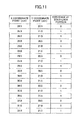
- FIG. 11 illustrates an example result determined by the calculation illustrated in FIG. 10 .
- Flags “1” are given to the meshes in which the solid lack portion is determined to exist, and flags “0” are given to the meshes in which the solid lack portion is determined not to exist. These flags are used when the shift amounts of the characteristic impedances are calculated by the impedance calculation unit 215 .
- the areas of the solid lack portion in each section of the wiring pattern 6 B are expressed as a value obtained by multiplying the number of the flags “1” by the unit area of the meshes of 0.25 mm 2 .
- the determination results of the wiring pattern 6 B are illustrated in FIG. 11 . However, determination results of all sections of the wiring patterns 6 , which correspond to the attribute information created by the condition creating part 212 , are obtainable in a similar manner.
- FIG. 12 illustrates the characteristic impedance of the wiring pattern 6 B influenced by the solid lack portion 8 A illustrated in FIG. 10 .
- the impedance calculation unit 215 creates a graph of the impedance based on the characteristics illustrated in FIG. 8 and the determination results of the existence of the solid lack portion 8 A relative to the X and Y coordinate points illustrated in FIG. 11 .
- the impedance calculation unit 215 calculates the characteristic impedances in the sections of the wiring pattern using the characteristics illustrated in FIG. 8 and the results illustrated in FIG. 11 .
- Characteristic impedance Increment coefficient ⁇ Area of solid lack portion+Offset value
- the increment coefficient has any one of the characteristics ( 1 ) through ( 3 ) illustrated in FIG. 8 .
- the offset value is determined as 50 ⁇ .
- the characteristic impedances of the sections of the wiring pattern 6 B are obtained by the impedance calculation unit 215 .
- the characteristic impedances may be similarly obtained for all wiring patterns 6 by the impedance calculation unit 215 .
- the model generating part 216 obtains the impedances of the wiring patterns 6 from the start coordinate points to the end coordinate points by integrating the values of the sections of the characteristic impedances obtained by the impedance calculation unit 215 from the start coordinate points to the end coordinate points of the wiring patterns 6 .
- FIG. 13 illustrates a calculation result of the characteristic impedances in the sections of the wiring pattern 6 obtained by the simulation apparatus of Embodiment 1.
- the table illustrates data of the calculation result of the characteristic impedances of the wiring pattern 6 B.
- the data are stored in the HDD 24 .
- the X and Y coordinate points illustrated in FIG. 13 represent the start coordinate points of the sections of the wiring pattern 6 B.
- FIG. 14 is an example flow chart illustrating a calculation process for supporting the tests for printed wiring boards carried out by the simulation apparatus of Embodiment 1.
- the CPU 21 executes the simulation program of Embodiment 1 to carry out the calculation illustrated in FIG. 14 .
- step S 1 the CPU 21 reads CAD data stored in the HDD 24 after starting the calculation. Step S 1 is carried out by the design data reading part 211 included in the CPU 21 . The CAD data illustrated in FIG. 5 are read out.
- step S 2 the CPU 21 creates conditions for calculating the shift amount of characteristic impedances.
- the process is to create the conditions for calculating the shift amount of the characteristic impedances based on the conditions input via the keyboard 13 or the mouse 14 .
- Step S 2 is carried out by the condition creating part 212 included in the CPU 21 .
- the input conditions are, for example, signal types transmitted through the wiring patterns 6 , the ranges in the width direction in which the shift amounts of the characteristic impedances are calculated, and threshold values of the impedances for extracting the impedances to rank these.
- step S 3 the CPU 21 classifies positional relationships between the wiring patterns 6 and solid lack portion 8 when the printed wiring boards 5 are being transparently viewed in plan (in the direction orthogonal to the printed wiring boards 5 ), and creates data indicative of the classification result.
- Step S 3 is to create a classification table illustrated in FIG. 7 based on the X and Y coordinate points of the wiring patterns 6 illustrated in FIG. 5A , and the X and Y coordinate points of the solid lack portions 8 illustrated in FIG. 5B .
- Step S 3 is carried out by the solid lack portion detecting part 213 included in the CPU 21 .
- step S 4 the CPU 21 extracts the wiring patterns 6 corresponding to the signal types transmitted by the wiring patterns 6 and created by the condition creating part 212 , and calculates the area of the solid lack portions 8 existing in the range in the width direction in which the shift amount of the characteristic impedances is calculated when the printed wiring boards 5 are being transparently viewed in plan (in the direction orthogonal to the printed wiring boards 5 ).
- Step S 4 is carried out by the area calculating part 214 .
- step S 5 the CPU 21 calculates the shift amounts of the characteristic impedances of the wiring pattern 6 to be calculated using the positional relationship between the wiring pattern 6 and the solid lack portion 8 classified by the solid lack portion detecting part 213 and the area of the solid lack portion 8 calculated by the area calculating part 214 in step S 5 .
- Step S 5 is carried out by the impedance calculation unit 215 included in the CPU 21 .
- the shift amount of the characteristic impedances is calculated for each section of the wiring pattern 6 , for example, each section divided every 0.5 mm being the length of the mesh side illustrated in FIG. 10 .
- Step S 6 the CPU 21 integrates the shift amounts of the characteristic impedances of the predetermined sections which are calculated in Step S 5 from the start coordinate points to the end coordinate points to generate a simulation model of the wiring pattern 6 .
- Step S 6 is carried out by the model generating part 216 included in the CPU 21 .
- the model generating part 216 integrates the values of the characteristic impedances of the sections, obtained by the impedance calculation unit 215 illustrated in FIG. 13 .
- Step S 7 the process result display part 217 displays the calculation result obtained by the impedance calculation unit 215 or the simulation model generated by the model generating part 216 on the display screen 12 A of the display 12 illustrated in FIG. 1 .
- the contents of the display are described later.
- FIG. 15 is a flow chart illustrating an example process of calculating the characteristic impedances with a model generating part 316 of the simulation apparatus of Embodiment 1.
- the one end is referred to as a transmitting end, and the other end is referred to as a receiving end.
- the number of the sections which have the same values of the characteristic impedances are referred to as the number of continuous sections.
- step S 11 when the process is started, the model generating part 216 sets “0” to the number of the continuous sections.
- step S 12 the model generating part 216 sets an initial value for integration to the characteristic impedance of the section connected to the transmitting end.
- the value of the characteristic impedance in the first section having the length of 0.5 mm of the wiring pattern 6 A and being connected to the transmitting end is read from the HDD 24 .
- the read value is set as the initial value of the calculation.
- step S 13 after step S 12 ends, the model generating part 216 processes the next section.
- the model generating part 216 integrates the value of the characteristic impedance of the next section.
- step S 14 the model generating part 216 determines whether the value of the characteristic impedance of the section is the same as the characteristic impedance of the previous section in step S 12 .
- step S 15 in a case where the model generating part 216 determines that the values of the characteristic impedances are not the same, the model generating part 216 generates a simulation model using the sections processed by then.
- the simulation model is temporarily stored in a RAM of the memory part 22 or the like. The simulation model is described later in reference to FIG. 16 .
- step S 16 the model generating part 216 sets “0” to the number of continuous sections.
- step S 17 when step S 16 ends the model generating part 216 determines whether the final section is processed. When the final section is not processed yet, the process goes back to step S 13 .
- Step S 14 determines whether the section currently processed is still continuous to the previously processed section.
- step S 19 in the case where the model generating part 216 determines that the currently processed section is the final section in step S 17 , the simulation model generated by then and stored in the memory part 22 is output. Thus, the process of generating the simulation model (wiring model) with the model generating part 216 ends.
- FIG. 16 illustrates an example simulation model (wiring model) generated by the simulation apparatus of Embodiment 1.
- the sections of which values of the characteristic impedances are the same are expressed as a continuous simulation model (section model). At points where the values of the characteristic impedances change, the simulation models (section model) discontinue.
- the simulation model (wiring model) illustrated in FIG. 16 and generated by the model generating part 216 is displayed on the display screen 12 A of the display 12 illustrated in FIG. 1 by the process result display part 217 .
- the simulation device of Embodiment 1 may calculate the shift amount of the characteristic impedances including influences of minute solid lack portions 8 near the wiring pattern 6 using the CAD data. Therefore, it is possible to design wirings of a printed wiring board which transmit high speed signals in consideration of a minute signal characteristic change.
- the wiring patterns which transmit relatively important signals are selected in advance from a large number of the wiring patterns 6 , it is possible to specify the wiring pattern which has a large shift amount of the characteristic impedances and transmits the relatively important signal.
- Such an important wiring pattern transmitting the relatively important signal may be selected in reference to the attributes (signal types or signal names of transmitted signal) of the wiring patterns 6 . Therefore, it is unnecessary to calculate for all of the wiring patterns 6 . Therefore, it is possible to efficiently simulate the wiring pattern while reducing the number of the processes.
- the shift amount of the characteristic impedances can be calculated by setting the range in the width direction of the wiring pattern 6 , the amount of the calculations can be reduced. Thus, an efficient simulation can be carried out.
- the shift amount of the characteristic impedances are calculated based on the area of the solid lack portions 8 of the solid pattern 7 , it is possible to easily calculate the shift amount of the characteristic impedances using the CAD data.
- FIG. 17A and FIG. 17B illustrate another way of calculating the area of solid lack portions 8 on a solid pattern 7 with the simulation apparatus of Embodiment 1.
- the solid lack portion 8 in a range in a width direction is divided to meshes between the start coordinate point and the end coordinate point of the wiring pattern 6 .
- the shift amount of characteristic impedances is obtained based on all of the unit areas.
- a simulation apparatus of Embodiment 2 calculates a shift amount of signal characteristics caused by cross talk. Since the simulation apparatus of Embodiment 1 calculates the shift amount of the characteristic impedances, the use of the signal characteristics caused by cross talk in Embodiment 2 is different from the use of the characteristic impedances in Embodiment 1.
- FIG. 18 is an example perspective view illustrating positional relationships between the wiring patterns 6 B and 6 C and the solid lack portion 8 A on the solid pattern 7 .
- the wiring pattern 6 B is formed in the third dielectric layer 5 c .
- the solid lack portion 8 A is formed on the solid pattern 7 on the fourth dielectric layer 5 d .
- the wiring pattern 6 C is formed on the fifth dielectric layer 5 e .
- the dielectric layers 5 c through 5 e are omitted for convenience of the description.
- a signal via hole or a ground via hole is formed inside the solid lack portion 8 A.
- illustration of the signal via hole and the ground via hole is omitted for convenience of the description.
- FIG. 19 schematically illustrates example positional relationships between the wiring patterns 6 B and 6 C and the solid lack portion 8 A on the solid pattern 7 illustrated in FIG. 18 .
- the wiring pattern 6 C is positioned immediately below the solid lack portion 8 A when the printed wiring boards 5 are being transparently viewed in plan (in the direction orthogonal to the printed wiring boards 5 ).
- the simulation apparatus of Embodiment 2 the area of cross talk regions is calculated, and the calculated area is multiplied by a coefficient for obtaining noise caused by the cross talk.
- the shift amount of signal characteristics can be simulated.
- the cross talk region is a region in which the wiring pattern 6 overlaps an inside portion 8 a surrounded by a dotted circle line and existing inside the range in the width direction of the wiring pattern described in Embodiment 1. Said differently, the cross talk region is a region in which the solid lack portion 8 and the wiring pattern 6 overlap within the range in the width direction of the wiring pattern 6 . Referring to FIG. 19 , a portion of the wiring pattern 6 C surrounded by the dotted circular line is the cross talk region.
- FIG. 20 is an example functional block chart illustrating the simulation apparatus of Embodiment 2. The function illustrated in FIG. 20 is demonstrated when the CPU 21 illustrated in FIG. 2 executes a printed wiring board support program stored in the HDD 24 .
- the functional block demonstrated by the CPU 21 includes a design data reading part 311 , a condition creating part 312 , a crosstalk region detecting part 313 , an area calculating part 314 , a shift amount calculating unit 315 , a model generating part 316 , a process result display part 317 and a management part 318 .
- a design data reading part 311 includes a design data reading part 311 , a condition creating part 312 , a crosstalk region detecting part 313 , an area calculating part 314 , a shift amount calculating unit 315 , a model generating part 316 , a process result display part 317 and a management part 318 .
- a design data reading part 311 includes a design data reading part 311 , a condition creating part 312 , a crosstalk region detecting part 313 , an area calculating part 314 , a shift amount calculating unit 315 , a model generating part 316 , a process result display part
- the design data reading part 311 carries out the same processes as those of the design data reading part 211 of Embodiment 1.
- the condition creating part 312 creates conditions for calculating the shift amount of the characteristic impedances described later based on conditions input via the keyboard 13 or the mouse 14 .
- the input conditions are signal types, a range in the width direction in which the shift amount of signal characteristics caused by the cross talk is calculated, and the length of the mesh sides used for calculating the area of the cross talk region.
- the crosstalk region detecting part 313 classifies positional relationships between a solid lack portion 8 and a wiring pattern 6 and between the solid lack portion 8 and another wiring pattern 6 which can be viewed through the solid lack portion 8 , when the printed wiring boards 5 are being transparently viewed in plan (in the direction orthogonal to the printed wiring boards 5 ), based on the X and Y coordinate points of the wiring patterns 6 illustrated in FIG. 5A and the X and Y coordinate points of the solid lack portion 8 illustrated in FIG. 5B .
- the area calculating part 314 extracts the wiring pattern 6 to be processed in reference to the signal types which are transmitted by the wiring patterns 6 and created by the condition creating part 312 , and calculates the area of cross talk regions existing in the range in the width direction in which the strength of the cross talk is calculated.
- the cross talk region is a region in which the solid lack portion 8 and the wiring pattern 6 overlaps within the range in the width direction of the wiring pattern 6 . Therefore, the shift amount of the signal characteristics is calculated by the simulation apparatus of Embodiment 2 using the area of the solid lack portions 8 .
- the shift amount calculating unit 315 calculates the strength of the cross talk as the shift amount of the signal characteristics of the wiring patterns 6 to be processed using the positional relationships between the wiring patterns 6 and the solid lack portion 8 obtained by the crosstalk region detecting part 313 and the area of the cross talk regions calculated by the area calculating part 314 .
- the model generating part 316 obtains the impedances of the wiring patterns 6 from the start coordinate points to the end coordinate points by integrating the values of predetermined sections of the characteristic impedances obtained by the impedance calculation unit 315 from the start coordinate points to the end coordinate points of the wiring patterns 6 . Thus, simulation models of the wiring patterns 6 are generated.
- the process result display part 317 displays the calculation results obtained by the impedance calculation unit 215 or the simulation models generated by the model generating part 316 on the display screen 12 A of the display 12 illustrated in FIG. 1 .
- the contents of the display are described later.
- the management part 318 administers storage of data in the HDD 24 .
- FIG. 21 is a table illustrating the strength of cross talk in unit areas of cross talk regions which are used in the simulation apparatus of Embodiment 2.
- the table illustrated in FIG. 21 includes data used for calculating the strength of the cross talk as indexes of measuring the shift amount of the signal characteristics.
- the strength is illustrated as noise per unit area of the cross talk regions relative to the dielectric constants of the dielectric layers and the interlayer distances.
- the distance between the wiring patterns 6 is measured when the printed wiring boards 5 are being transparently viewed in plan (in the direction orthogonal to the printed wiring boards 5 ). Referring back to FIG. 19 , the distance is between the wiring patterns 6 B and 6 C. Referring back to FIG. 19 , the distance between the wiring pattern 6 and the solid lack portion 8 is an interval (offset) between the wiring pattern 6 B and the solid lack portion 8 A.
- FIG. 23 illustrates calculation of the area of cross talk regions used in calculating the strength of cross talk with the simulation apparatus of Embodiment 2.
- the crosstalk region detecting part 313 calculates the area of the cross talk regions.
- the calculation of the area is carried out as follows. A region from the start coordinate point to the end coordinate point of the wiring pattern 6 to be calculated to obtain the shift amount of the signal characteristics is divided into square meshes having predetermined square areas from the start coordinate point to the end coordinate point. Then, it is determined whether the solid lack portions 8 and the wiring patterns 6 exist in any of the meshes.
- a drop time may be used instead of or in addition to the rise time.
- the cross talk regions are a portion of the wiring pattern 6 C which can be viewed through the solid lack portion 8 A in a manner similar to FIG. 19 .
- FIG. 24 is an example table including results of determination illustrated in FIG. 23 and results of extracting distances between the wiring patterns.
- the mesh in which the cross talk region is determined to exist the cross talk region is indicated by a flag “1”, and the mesh in which the cross talk region is determined to not exist is indicated by a flag “0”.
- the flag is used when the shift amount calculating unit 315 calculates the strength of the cross talk.
- the shift amount calculating unit 315 selects the noise per unit area from the table illustrated in FIG. 21 using the dielectric constant and the interlayer distance included in the CAD data.
- the shift amount calculating unit 315 selects the correction coefficient from the table illustrated in FIG. 22 using the positional data included in the CAD data and the distance between the wiring patterns illustrated in FIG. 24 .
- the strengths of cross talk per unit area calculated by the shift amount calculating unit 315 based on Formula 4 are integrated from the start coordinate point to the end coordinate point of the wiring pattern 6 in a manner similar to the characteristic impedances per unit area in Embodiment 1. Thus, the integration of the strengths of the cross talk are obtainable.
- simulation model (wiring model) is generated by the model generating part 316 in a manner similar to Embodiment 1.
- the area of the cross talk regions is calculated and the strength of cross talk is calculated. Therefore, when the wiring patterns which transmit relatively important signals are selected from a large number of the wiring patterns 6 , it is possible to easily specify the wiring pattern which has a great strength of cross talk and transmits the relatively important signals.
- Such important wiring patterns transmitting the relatively important signals may be selected in reference to the attributes (signal types or signal names of transmitted signals) of the wiring patterns 6 . Therefore, it is unnecessary to calculate all of the wiring patterns 6 . Therefore, it is possible to efficiently simulate the wiring pattern by reducing the number of the processes.
- the simulation apparatus of Embodiment 2 may be combined with the simulation apparatus of Embodiment 1. Said differently, both the shift amount of the characteristic impedances and the influence of the cross talk may be considered in simulating the shift amount of the signal characteristics.
- an eye pattern is produced using the characteristic impedances of Embodiment 1, and the strength of cross talk of Embodiment 2 may be superposed as noise.
- the waveforms substantially overlap at plural positions, for example, timings and voltages of the waveforms are the same, the waveforms have a good quality.
- the noise generated by the cross talk is superposed on the eye pattern and may be displayed on the display screen 12 A of the display 12 .
- the size of the eye pattern may be evaluated without a great number of calculations.
- a designer can evaluate the signal characteristics of a wiring pattern in the vicinity of a solid lack portion.
- the production of the eye pattern and the superposition of the noise may be carried out by an eye pattern processing part 319 as a function of the CPU 21 .
- FIG. 26 is an example functional block chart illustrating a simulation apparatus of Embodiment 3.
- the simulation apparatus of Embodiment 3 uses the eye pattern of Embodiment 2 to extract a wiring pattern having a small time axis margin and a small voltage axis margin. This extraction process is carried out by the eye pattern processing part 319 .
- the functional blocks of the simulation apparatus of Embodiment 3 have a structure similar to the functional blocks of the simulation apparatus of Embodiment 2.
- the functional block of an eye pattern processing part 319 is added to the functional blocks of the simulation apparatus of Embodiment 2.
- a determination process carried out by the eye pattern processing part 319 is described.
- the eye pattern is basically the same as that illustrated in FIG. 25 .
- the time axis margin is a margin between a mask and an eye pattern or between the mask and noise in the time axis direction.
- the voltage axis margin is a margin between the mask and the eye pattern or between the mask and the noise in the voltage axis direction.
- the minimum time axis margin is obtainable by calculating with the eye pattern processing part 319 the smaller one of margins between two apexes of the mask in a hexagonal shape along the time axis and the eye pattern or the smaller one of margins between the two apexes of the mask and the noise.
- the smaller voltage axis margin is obtainable by calculating with the eye pattern processing part 319 the smaller one of margins between four apexes of the mask along the voltage axis or the smaller one the eye pattern and margins between the four apexes of the mask and the noise, for example.
- FIG. 27A and FIG. 27B are an example flow chart illustrating a determination process with the simulation apparatus of Embodiment 3. Referring to FIG. 27A and FIG. 27B , an additional determination process is carried out by the eye pattern processing part 319 .
- the simulation apparatus extracts a wiring pattern 6 of which degradation level of the signal characteristics is high using the observation of the eye pattern, the result of calculating the area of the solid lack portions, the wiring length of the wiring pattern 6 , a preemphasis level, and an equalizer level.
- Data indicating the area of the solid lack portions 8 from the start coordinate point to the end coordinate point, the wiring length, the preemphasis level and the equalizer level concerning the wiring pattern 6 which has been selected using the attribute of the signal name are stored in the HDD 24 by the condition creating part 212 when the processes illustrated in FIG. 27A and FIG. 27B are carried out.
- the identifier of the wiring pattern 6 is associated with the data and stored in the HDD 24 by the condition creating part 212 .
- step S 20 the eye pattern processing part 319 produces an eye pattern for the wiring pattern 6 which is first calculated.
- step S 21 the eye pattern processing part 319 stores data indicating the eye pattern produced in step S 20 in association with the data indicating the area of the solid lack portions 8 , the wiring length, the preemphasis level and the equalizer level of the wiring pattern and with the identifier of the wiring pattern 6 in the HDD 24 .
- step S 21 the eye pattern processing part 319 stores data forming the eye pattern produced in step S 20 in association with the data indicating the area of the solid lack portions 8 , the wiring length, the preemphasis level and the equalizer level of the wiring pattern and with the identifier of the wiring pattern 6 in the HDD 24 .
- step S 23 the eye pattern processing part 319 determines whether the preemphasis level and the equalizer level in the data read in step S 22 are the same as the preemphasis level and the equalizer level in the data of the wiring pattern first processed in step S 20 .
- step S 24 after Yes in step S 23 , the eye pattern processing part 319 determines whether a difference between the wiring lengths of the wiring pattern 6 first processed in step S 20 and the wiring length of the wiring pattern 6 read in step S 22 is within ⁇ 10%.
- step S 25 after Yes in step S 24 , the eye pattern processing part 319 determines whether a difference between the area of the solid lack portions 8 relative to the wiring pattern 6 first processed in step S 20 and the area of the solid lack portions 8 relative to the wiring pattern 6 read in step S 22 is within ⁇ 10%.
- step S 25 the eye pattern processing part 319 returns to step S 22 without producing the eye pattern, and further reads data of the next wiring pattern indicating the area of the solid lack portions 8 relative to the wiring pattern 6 , the wiring length of the wiring pattern 6 , the preemphasis level and the equalizer level. Since the wiring pattern 6 first processed in step S 20 is similar to the wiring pattern 6 read in step S 22 , it is considered that the production of the eye pattern is unnecessary.
- step S 26 after No in step S 23 , No in step S 24 or No in step S 25 , the eye pattern processing part 319 produces the eye pattern and stores the data forming the eye pattern in the HDD 24 . Because the areas of the solid lack portions 8 and the wiring lengths concerning the wiring patterns 6 first processed in step S 20 and the wiring pattern 6 read in step S 22 are not similar, the shapes of the eye patterns may be largely different. Therefore, the eye pattern is newly produced.
- step S 27 the eye pattern processing part 319 determines whether the wiring pattern whose eye pattern is produced in step S 26 is the final wiring pattern among the wiring patterns 6 selected using the attribute information such as the signal name. Said differently, it is determined whether all wiring patterns 6 selected using the signal name are processed.
- step S 27 the process returns to step S 21 when the eye pattern processing part 319 determines that the wiring pattern is not the final wiring pattern. This is to completely process the wiring patterns 6 selected using the attribute information such as the signal name.
- the eye pattern processing part 319 determines the wiring pattern is the final one in step S 27 , the eye pattern processing part 319 reads the data forming the eye patterns of the wiring patterns, which eye patterns are produced in steps S 20 and S 27 , from the HDD 24 . In step S 28 , the eye pattern processing part 319 extracts the eye pattern whose margin is provisionally the smallest.
- the margin may be any one or both of the time axis margin and the voltage axis margin.
- step S 29 the eye pattern processing part 319 stores the wiring pattern extracted in step S 28 as a candidate of the wiring pattern 6 having the smallest margin.
- step S 29 is carried out by giving a flag indicating the candidate of the wiring pattern 6 having the smallest margin to the candidate of the data forming the wiring pattern 6 having the smallest margin.
- step S 30 the eye pattern processing part 319 selects the first wiring pattern 6 , and reads data indicating the area of the solid lack portions 8 relative to the first wiring pattern 6 , the wiring length of the first wiring pattern 6 , the preemphasis level and the equalizer level.
- step S 31 the eye pattern processing part 319 determines whether the preemphasis level and equalizer level of the candidate of the wiring pattern 6 having the smallest margin are the same as those of the first wiring pattern 6 which is being processed.
- step S 32 after Yes in step S 31 , the eye pattern processing part 319 determines whether a difference between the wiring length of the candidate of the wiring pattern 6 having the smallest margin and the wiring length of the wiring pattern 6 selected in step S 30 is within ⁇ 10%, and whether a difference between the area of the solid lack portions 8 relative to the candidate of the wiring pattern 6 having the smallest margin and the area of the solid lack portions 8 relative to the wiring pattern 6 selected in step S 30 is within ⁇ 10%.
- step S 33 after YES is step S 32 , the eye pattern processing part 319 produces the eye pattern of the wiring pattern 6 which is being processed.
- step S 34 after producing the eye pattern the eye pattern processing part 319 reads data of the next wiring pattern indicating the area of the solid lack portions 8 relative to the wiring pattern 6 , the wiring length of the wiring pattern 6 , the preemphasis level and the equalizer level for the next wiring pattern.
- step S 31 or step S 32 the eye pattern processing part 319 brings the process to step S 34 .
- step S 35 the eye pattern processing part 319 determines whether the wiring pattern being processed is the final wiring pattern. In step S 35 , the eye pattern processing part 319 brings the process back to step S 31 when the eye pattern processing part 319 determines that the wiring pattern is not the final wiring pattern.
- step S 35 When the flow returns from step S 35 to step S 31 , the wiring pattern 6 processed in steps S 31 thru S 33 becomes the wiring pattern read in step S 34 .
- step S 36 the eye pattern processing part 319 extracts the eye pattern whose margin is the smallest.
- step S 36 the wiring pattern 6 whose margin is the smallest is fixed.
- step S 37 the eye pattern processing part 319 outputs the result of the processes.
- the eye pattern processing part 319 displays the identification number of the wiring pattern 6 whose margin is the smallest on the display screen 12 A of the display 12 illustrated in FIG. 1 .
- the simulation apparatus of Embodiment 3 can extract the candidates of the wiring patterns whose margins are provisionally the smallest out of all the wiring patterns as a first stage. Then, the simulation apparatus of Embodiment 3 can fix the wiring whose margin is the smallest out of the wiring patterns selected using the signal names or the like without producing eye patterns for all of the wiring patterns as a second stage. In the second stage, the areas of the solid lack portions, the wiring lengths, the preemphasis levels and the equalizer levels are compared between the candidates of the wiring pattern having the smallest margin and all the wiring patterns 6 .
- the wiring pattern 6 whose margin is the smallest has a signal characteristic in a high degradation level. It is possible to extract a wiring pattern 6 having a large degradation level while using eye patterns and fewer processes in Embodiment 3.
- the processes can be carried out using values indicating shift amounts of the characteristic impedances instead of the areas of the solid lack portions.
- the impedance calculation unit 215 generates the simulation model (wiring model) after obtaining specific values of the characteristic impedances.
- a simulation apparatus of Embodiment 4 is different from Embodiment 1 at a point in which the impedance calculation unit 215 generates a simulation model (wiring model) using an area of solid lack portions existing between a start coordinate point and an end coordinate point.
- the area of the solid lack portions is used as a value indicating a shift amount of signal characteristics.
- the other structure is the same as that of the simulation apparatus of Embodiment 1. Therefore, the same reference symbols are used for the same structural elements as those of the simulation apparatus of Embodiment 1, and description of these structural elements is omitted.
- the impedance calculation unit 215 obtains the area of the solid lack portions existing between the start coordinate point and the end coordinate point of a wiring pattern 6 in a range in a width direction in which shift amounts of characteristic impedances are calculated by integrating the areas of the solid lack portions calculated by the area calculating part 214 from the start coordinate point to the end coordinate point of the wiring pattern 6 .
- the impedance calculation unit 215 of Embodiment 4 generates the simulation model (wiring model) by integrating the areas of the solid lack portions in the range determined by Formula 2 from the start coordinate point to the end coordinate point without multiplying the increment coefficients illustrated in FIG. 8 .
- FIG. 28 illustrates an example simulation model (wiring model) generated by the simulation apparatus of Embodiment 4.
- Sections in which the areas of the solid lack portions are the same is a continuous simulation model (section model).
- the continuous simulation model (section model) is interrupted at a point at which the values of the areas of the solid lack portions are different.
- Embodiment 4 in comparison with Embodiment 1, the area of the solid lack portions causing signal characteristic degradation is obtained instead of calculating the deviation of the characteristic impedances.
- the generation of the simulation model using the area of a region causing degradation of the signal characteristic may be applied to Embodiments 2 and 3.
- the simulation model (wiring model) is generated base on the result of calculation of the area of a cross talk region.
- an eye pattern may be produced based on the calculation result of a cross talk area.
Landscapes
- Engineering & Computer Science (AREA)
- Physics & Mathematics (AREA)
- Theoretical Computer Science (AREA)
- Computer Hardware Design (AREA)
- Evolutionary Computation (AREA)
- Geometry (AREA)
- General Engineering & Computer Science (AREA)
- General Physics & Mathematics (AREA)
- Computer Networks & Wireless Communication (AREA)
- Design And Manufacture Of Integrated Circuits (AREA)
Abstract
Description
Length of mesh side=Rise time×Transmitting velocity/Arbitrary divided
Characteristic impedance=Increment coefficient×Area of solid lack portion+Offset
Length of mesh side=Rise time×Transmitting velocity/Arbitrary divided
Strength of cross talk=Noise per unit area×
Claims (12)
Applications Claiming Priority (2)
| Application Number | Priority Date | Filing Date | Title |
|---|---|---|---|
| JP2009-171566 | 2009-07-22 | ||
| JP2009171566A JP5267369B2 (en) | 2009-07-22 | 2009-07-22 | Simulation device, simulation method, simulation program |
Publications (2)
| Publication Number | Publication Date |
|---|---|
| US20110022364A1 US20110022364A1 (en) | 2011-01-27 |
| US8204722B2 true US8204722B2 (en) | 2012-06-19 |
Family
ID=43498057
Family Applications (1)
| Application Number | Title | Priority Date | Filing Date |
|---|---|---|---|
| US12/830,661 Expired - Fee Related US8204722B2 (en) | 2009-07-22 | 2010-07-06 | Simulation apparatus, simulation method, and simulation program |
Country Status (2)
| Country | Link |
|---|---|
| US (1) | US8204722B2 (en) |
| JP (1) | JP5267369B2 (en) |
Citations (3)
| Publication number | Priority date | Publication date | Assignee | Title |
|---|---|---|---|---|
| JPH0981602A (en) | 1995-09-12 | 1997-03-28 | Zuken:Kk | Calculation device for power supply pattern and ground pattern on printed board |
| JP2001331539A (en) | 2000-05-22 | 2001-11-30 | Sony Corp | Wiring structure check system for printed board |
| JP2008015636A (en) | 2006-07-04 | 2008-01-24 | Nec Corp | Method, program and apparatus for creating model of equivalent circuit |
Family Cites Families (4)
| Publication number | Priority date | Publication date | Assignee | Title |
|---|---|---|---|---|
| JP3264806B2 (en) * | 1994-11-15 | 2002-03-11 | 富士通株式会社 | Circuit simulation model extraction method and apparatus |
| JP3217931B2 (en) * | 1995-02-15 | 2001-10-15 | 沖電気工業株式会社 | Crosstalk simulation method for design board |
| JP4378846B2 (en) * | 2000-05-26 | 2009-12-09 | ソニー株式会社 | Printed circuit board wiring structure check system and printed circuit board wiring structure check method |
| JP3975841B2 (en) * | 2002-06-28 | 2007-09-12 | ソニー株式会社 | Circuit board verification method and verification apparatus |
-
2009
- 2009-07-22 JP JP2009171566A patent/JP5267369B2/en not_active Expired - Fee Related
-
2010
- 2010-07-06 US US12/830,661 patent/US8204722B2/en not_active Expired - Fee Related
Patent Citations (3)
| Publication number | Priority date | Publication date | Assignee | Title |
|---|---|---|---|---|
| JPH0981602A (en) | 1995-09-12 | 1997-03-28 | Zuken:Kk | Calculation device for power supply pattern and ground pattern on printed board |
| JP2001331539A (en) | 2000-05-22 | 2001-11-30 | Sony Corp | Wiring structure check system for printed board |
| JP2008015636A (en) | 2006-07-04 | 2008-01-24 | Nec Corp | Method, program and apparatus for creating model of equivalent circuit |
Also Published As
| Publication number | Publication date |
|---|---|
| JP5267369B2 (en) | 2013-08-21 |
| JP2011028401A (en) | 2011-02-10 |
| US20110022364A1 (en) | 2011-01-27 |
Similar Documents
| Publication | Publication Date | Title |
|---|---|---|
| CN101963651B (en) | Printed circuit board test assisting apparatus and printed circuit board test assisting method | |
| JP5396502B2 (en) | Wiring board design system, design data analysis method and analysis program | |
| US8296715B2 (en) | Wiring design assisting apparatus, wiring design assisting method, and computer-readable information recording medium | |
| EP2378446A2 (en) | Coupled analysis simulation apparatus and coupled analysis simulation method | |
| JP4294647B2 (en) | Printed circuit board design device and CAD system | |
| JP2009238130A (en) | Printed circuit board designing apparatus and printed circuit board designing method | |
| JP2010262338A (en) | Electromagnetic flow distribution processing apparatus, electromagnetic flow distribution processing method, and electromagnetic flow distribution processing program | |
| US20030084412A1 (en) | Automated crosstalk identification system | |
| WO2014080610A1 (en) | Circuit substrate design system, circuit substrate design method, and program recording medium | |
| US8204722B2 (en) | Simulation apparatus, simulation method, and simulation program | |
| JP2018088056A (en) | Via model generation program, via model generation method, and information processing apparatus | |
| JP2010039598A (en) | Wiring display device and method for multilayer printed circuit board | |
| JP4283647B2 (en) | Layout check system | |
| JP5082793B2 (en) | Printed circuit board design support apparatus, printed circuit board design support method, and printed circuit board design support program | |
| JP4768380B2 (en) | Wiring board design system, design data analysis method and analysis program | |
| JPH1097560A (en) | Computer aided design system | |
| JP2001092874A (en) | Printed board designing device | |
| US7313509B2 (en) | Simulation method and apparatus, and computer-readable storage medium | |
| JP2007241802A (en) | Board design support apparatus, printed circuit board, board design support program, and board design support method | |
| JP4862695B2 (en) | Circuit board design system, circuit board design method, and computer program for circuit board design | |
| JP4071351B2 (en) | Printed circuit board design CAD system | |
| JP2001067390A (en) | Design device for printed circuit board | |
| JP2007257572A (en) | Circuit characteristic calculation device, circuit characteristic calculation program, and circuit characteristic calculation method | |
| JP2006039909A (en) | Electric circuit board design support device and design rule check device | |
| JP2011043981A (en) | Return current route check system, return current route check method and electronic apparatus |
Legal Events
| Date | Code | Title | Description |
|---|---|---|---|
| AS | Assignment |
Owner name: FUJITSU LIMITED, JAPAN Free format text: ASSIGNMENT OF ASSIGNORS INTEREST;ASSIGNOR:TSUBAMOTO, DAITA;REEL/FRAME:024703/0033 Effective date: 20100531 |
|
| STCF | Information on status: patent grant |
Free format text: PATENTED CASE |
|
| FEPP | Fee payment procedure |
Free format text: PAYOR NUMBER ASSIGNED (ORIGINAL EVENT CODE: ASPN); ENTITY STATUS OF PATENT OWNER: LARGE ENTITY |
|
| FPAY | Fee payment |
Year of fee payment: 4 |
|
| FEPP | Fee payment procedure |
Free format text: MAINTENANCE FEE REMINDER MAILED (ORIGINAL EVENT CODE: REM.); ENTITY STATUS OF PATENT OWNER: LARGE ENTITY |
|
| LAPS | Lapse for failure to pay maintenance fees |
Free format text: PATENT EXPIRED FOR FAILURE TO PAY MAINTENANCE FEES (ORIGINAL EVENT CODE: EXP.); ENTITY STATUS OF PATENT OWNER: LARGE ENTITY |
|
| STCH | Information on status: patent discontinuation |
Free format text: PATENT EXPIRED DUE TO NONPAYMENT OF MAINTENANCE FEES UNDER 37 CFR 1.362 |
|
| FP | Lapsed due to failure to pay maintenance fee |
Effective date: 20200619 |