EP2377104B1 - Dispositif et procédé de détection de lumière réfléchie et/ou émise par un objet - Google Patents
Dispositif et procédé de détection de lumière réfléchie et/ou émise par un objet Download PDFInfo
- Publication number
- EP2377104B1 EP2377104B1 EP09801661.1A EP09801661A EP2377104B1 EP 2377104 B1 EP2377104 B1 EP 2377104B1 EP 09801661 A EP09801661 A EP 09801661A EP 2377104 B1 EP2377104 B1 EP 2377104B1
- Authority
- EP
- European Patent Office
- Prior art keywords
- light
- sensor
- reflected
- emitted
- illumination device
- Prior art date
- Legal status (The legal status is an assumption and is not a legal conclusion. Google has not performed a legal analysis and makes no representation as to the accuracy of the status listed.)
- Active
Links
- 238000000034 method Methods 0.000 title claims description 7
- 238000005286 illumination Methods 0.000 claims description 37
- 230000003287 optical effect Effects 0.000 claims description 24
- 230000000737 periodic effect Effects 0.000 claims description 6
- 238000001514 detection method Methods 0.000 claims description 3
- 230000003595 spectral effect Effects 0.000 description 5
- 230000005281 excited state Effects 0.000 description 3
- 239000003086 colorant Substances 0.000 description 2
- 238000010586 diagram Methods 0.000 description 2
- 239000011521 glass Substances 0.000 description 2
- 239000000976 ink Substances 0.000 description 2
- 230000010363 phase shift Effects 0.000 description 2
- 230000001681 protective effect Effects 0.000 description 2
- 230000005540 biological transmission Effects 0.000 description 1
- 238000000354 decomposition reaction Methods 0.000 description 1
- 230000006735 deficit Effects 0.000 description 1
- 230000000694 effects Effects 0.000 description 1
- 230000005284 excitation Effects 0.000 description 1
- 238000007689 inspection Methods 0.000 description 1
- 238000004519 manufacturing process Methods 0.000 description 1
- 238000005192 partition Methods 0.000 description 1
- 230000005855 radiation Effects 0.000 description 1
- 230000002123 temporal effect Effects 0.000 description 1
Images


Classifications
-
- G—PHYSICS
- G07—CHECKING-DEVICES
- G07D—HANDLING OF COINS OR VALUABLE PAPERS, e.g. TESTING, SORTING BY DENOMINATIONS, COUNTING, DISPENSING, CHANGING OR DEPOSITING
- G07D7/00—Testing specially adapted to determine the identity or genuineness of valuable papers or for segregating those which are unacceptable, e.g. banknotes that are alien to a currency
- G07D7/06—Testing specially adapted to determine the identity or genuineness of valuable papers or for segregating those which are unacceptable, e.g. banknotes that are alien to a currency using wave or particle radiation
- G07D7/12—Visible light, infrared or ultraviolet radiation
- G07D7/121—Apparatus characterised by sensor details
Definitions
- the invention is based on a device and a method for detecting reflected and / or emitted light of an object, in particular a flat object.
- Such devices are used in the inspection of objects. These include recognizing, controlling, verifying and verifying the authenticity of objects and identifying counterfeits.
- the items include in particular notes of value or documents such as banknotes, checks, stocks, papers with security imprint, certificates, tickets or tickets, vouchers, but also credit or debit cards, identification or access cards.
- Devices for detecting reflected and / or emitted light of an object are often part of a multi-component system for processing flat objects.
- Devices for detecting reflected and / or emitted light serve to distinguish counterfeit from real objects.
- the objects in particular banknotes, security, identity or value documents, are printed with suitable security printing inks. These give the viewer a certain color impression in the visible spectral range.
- a method and apparatus for measuring the lifetime of excited states by fluorescence is known.
- a sample is irradiated with light to excite fluorescence.
- the intensity of the exciting light changes repeatedly between a first intensity I 1 and a second intensity I 2 .
- the light emitted by the sample due to fluorescence is detected.
- a signal of the detected light is generated, which is decomposed into a first value S 1 and a second value S 2 .
- the decomposition corresponds to the intensities I 1 and I 2 of the exciting light.
- the lifetime of the excited state is calculated using a formula in which the values S 1 and S 2 , the period T concerning the switching between the intensities I 1 and I 2 and the service life T are received.
- a disadvantage proves that checking the authenticity of objects based on the lifetime of excited states is complex and therefore not in articles in large numbers during transport is not practical.
- the EP 1 220 165 A2 discloses a device for detecting fluorescence of a specific wavelength and of reflection in the UV range.
- the device has a UV LED as the light source. Furthermore, it is equipped with a detector for detecting the light reflected from an object to be examined and with a detector for detecting the fluorescence.
- the second detector is separated from the light source by a shield and equipped with a filter for the irradiated wavelength.
- the GB 2 366 371 A discloses a device for scanning bills.
- the light reflected from a bill is detected by a plurality of detectors arranged in a row.
- the output of each detector is processed by means of an analog low-pass filter, an A / D converter and finally a digital filter.
- the digital filter has a transfer function, that of the inverse of the transfer function corresponds to the analog filter.
- the digital filter is determined by means of a processor, which is connected via an A / D converter to a power source for multiple light sources.
- the light sources have different wavelengths and serve to illuminate the bills.
- the intensity of the light reflected or emitted by the object is either so high that the detector used for detection saturates or is so weak that the detector can not detect the effect. Since the objects to be inspected have differences in their optical properties, particularly in terms of their reflection, fluorescence and phosphorescence characteristics, the intensity of the reflected or emitted light can not be limited to a predetermined value or a narrow range and the detector or sensor can not be set to this range become.
- the device with the features of claim 1 has the advantage that it is equipped with a power supply for a lighting device, which supplies the lighting device with a temporally periodic current, wherein a period of time course has at least two current pulses with different amounts.
- the differently strong current pulses of the power supply lead to different intensities of the light pulses of the illumination device. Each area of the object is thereby irradiated with a strong and a weak light pulse.
- the frequency of the pulsed light and the temporal resolution of a sensor which detects the light reflected from the object and / or emitted by fluorescence and phosphorescence, is so high compared to the speed of the transport device that the movement of the object between two light pulses is negligible , It can therefore be approximately assumed that the Subject between the illumination with a strong and a weak light pulse rests.
- the sensors detect the light reflected and / or emitted by the object both in relation to the strong and to the weak
- the number of different current pulses per period of the time-periodic current can be increased.
- the current intensities of the current pulses and the duration of the current pulses in relation to the duration of the current value 0, which is referred to as the duty cycle, can be predetermined as a function of the objects to be examined. This also applies to the period or the frequency of the time-periodic current.
- Time periodic current in this case means that the current is a periodic function over time and thus has a periodicity over time.
- the inventive method with the features of claim 9 is characterized in that the illumination device irradiates the object with pulsed light, wherein within a period of the pulsed light at least two light pulses of different intensity are generated. This takes place in that the lighting device is supplied with a pulsed current by means of a power supply, wherein each period has at least two current pulses with different current intensity.
- the method can be carried out with the device according to claim 1.
- the illumination device has at least one light-emitting diode LED.
- excitation lamps such as fluorescent lamps and gas discharge lamps can be used instead, however, light emitting diodes LED are characterized by a compact dimensions, a lower manufacturing price, a faster response time and thus a higher frequency of light pulses, and a lower susceptibility to failure and repair out.
- the advantage in any case is the illumination with monochromatic light or at least light of a narrow spectral range. In this way it is easier to distinguish the fluorescence and phosphorescence of real objects on the one hand and counterfeit objects on the other hand.
- the light-emitting diode LED is a UV-emitting diode UV-LED.
- UV light has the advantage that the fluorescence and phosphorescence takes place in the visible spectral range or near the visible spectral range and can therefore be detected easily with optical sensors.
- the device is equipped with at least one first sensor for detecting the light reflected by the object and at least one second sensor for detecting the light emitted by the object by fluorescence and / or phosphorescence.
- the first and second sensors are in different positions.
- the illumination device in particular the light-emitting diode LED, is preferably arranged with its optical axis at an angle other than 0 ° and 90 ° to the transport direction of the transport device.
- the first sensor for detecting the light reflected from the object is arranged with its optical axis at the same angle to the surface of the object as the illumination device, but symmetrical to a plane perpendicular to the surface of the object and through the intersection between optical axis of the illumination device and the surface of the object runs.
- the second sensor may be in any position, for example, vertically above the surface of the article. This means that its optical axis is aligned perpendicular to the surface of the object. Since the wavelength of the reflected light is different from that of the emitted light, different sensors are used. The wavelength of the reflected light coincides with the wavelength of the light of the illumination device. The wavelength of the emitted light is less than that of the light of the illumination device.
- the second sensor is an RGB sensor.
- RGB stands for the abbreviation red green blue.
- This sensor is based on the three-color theory, in which the entire color space is made up of the superimposition of the colors red, green and blue. For each of the three primary colors, a separate sensor element is used.
- an optical shield is arranged between the illumination device and the second sensor. This prevents that the light of the illumination device leads to an impairment of the second sensor.
- a filter can be arranged on the illumination device, which filters out the typical wavelengths of fluorescence and phosphorescence from the light of the illumination device.
- the power supply of the illumination device is equipped with at least two input resistors connected in parallel and a differential amplifier. Furthermore, the power supply has a voltage source which supplies at least two pulsed input voltages.
- the number of pulsed input voltages coincides with the number of current pulses per period of the power supply.
- the frequency of one input voltage is twice the frequency of the other input voltage.
- the largest frequency is n times the smallest frequency.
- the maximum of the input voltages may be the same or different.
- the phase shift between the input voltages is 0. This particularly simple circuit with inexpensive components reliably generates a periodic current with at least two different current pulses per period.
- the sensors convert the light reflected or emitted by the article into an electrical signal proportional to the intensity of the light. It may be, for example, photodiodes or CCD. In this case, a plurality of such components can be arranged in a row or in an array. Furthermore, the sensor is equipped with an optical system, in particular a lens system. In addition, the sensor may include a filter to mask out those wavelengths of light that are to be detected with the other sensor. For example, the second sensor for detecting the light based on fluorescence and phosphorescence is equipped with a filter which absorbs the light in the wavelength range of the illumination device.
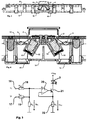
- Figures 1 and 2 show the basic structure of a device for detecting reflected and emitted light of an article 1.
- the article is a banknote.
- the object 1 is irradiated with light, which generates a lighting device 2.
- the lighting device 2 is a UV LED.
- the optical axis of the illumination device 2 is in FIG. 1 represented by an arrow 3.
- the light reflected from the surface of the article 1 is detected by a first sensor 4.
- the optical axis of the first sensor 4 is indicated by the arrow 5.
- the object 1 irradiated with the light of the illumination device 2 emits light whose wavelength differs from the incident light of the illumination device due to fluorescence and phosphorescence.
- a second sensor 6 is disposed above the article 1.
- the optical axis 7 of this second sensor 6 is perpendicular to the surface of the article 1.
- the detected by the first sensor 4 reflected light is in FIG. 1 symbolized by an arrow 8.
- the light emitted by fluorescence or phosphorescence is in FIG. 1 symbolized by the arrow 9.
- FIG. 2 shows the same schematic structure as FIG. 1 , Additionally are in FIG. 2 an optical shield 10 is shown between the illumination device 2 and the second sensor 6, and a filter 11 in front of the illumination device 2.
- the filter is a UV transmission filter which filters out the visible components of the light of the illumination device, in particular blue components .
- the second sensor 6 is an RGB sensor.
- the optical shield 10 in the form of a partition wall ensures that the UV radiation reflected directly by the object 1 does not reach the second sensor.
- FIG. 3 shows a complete device, which according to the principle FIGS. 1 and 2 is constructed.
- the device consists of two lighting devices 2, two not visible in the drawing first sensors and two second sensors 6. Both lighting devices 2 are equipped with UV-LED and a filter 11. They are each in a housing 12, which also serves as an optical shield against the two second sensors 6.
- the lighting devices 2 and the second sensors 6 are arranged on a printed circuit board 13 which is equipped with further electrical components. Printed circuit board and components arranged thereon are surrounded by a housing 14.
- the housing 14 is equipped with a protective glass 15 permeable to this light.
- FIG. 4 is the detail of the device according to FIG. 4 shown enlarged with the two illumination devices 2 and the second sensors 6.
- FIG. 5 shows a circuit diagram of the power supply of the lighting device to the device according to FIGS. 1 to 4 , Inputs 18 and 19 of a differential amplifier 20 are provided at the inputs 16 and 17 of the circuit.
- the two input resistors are connected in parallel.
- the input voltages U 1 and U 2 are generated by a digital component, not shown, for example a microcontroller, an FPGA or a CPLD.
- the differential amplifier determines the base current of a transistor 21 which is connected to the UV LED of the illumination device 2. The current through the diode is limited by a resistor 22.
- FIG. 6 a scheme of the time course of the two input voltages U 1 and U 2 is shown.
- the frequency of the input voltage U 1 is twice as large as that of the input voltage U 2 .
- the phase shift is 0.
- FIG. 7 shows that in the circuit according to FIG. 5 resulting from these input voltages time course of the current I LED of the LED of the illumination device.
- two current pulses 23 and 24 are generated.
- the current pulse 23 has a higher current than the current pulse 24.
- the duty cycle is 1/5. The strength of the current pulses and the duty cycle depend on the input voltages U 1 and U 2 and the input resistors 18 and 19.
Landscapes
- Health & Medical Sciences (AREA)
- General Health & Medical Sciences (AREA)
- Toxicology (AREA)
- Physics & Mathematics (AREA)
- General Physics & Mathematics (AREA)
- Investigating, Analyzing Materials By Fluorescence Or Luminescence (AREA)
- Inspection Of Paper Currency And Valuable Securities (AREA)
Claims (9)
- Dispositif de détection de lumière réfléchie et/ou émise par un objet (1) lors de la reconnaissance, du contrôle, de la vérification et de l'examen de l'authenticité d'objets,• avec au moins un dispositif d'éclairage (2), qui est conçu pour éclairer l'objet (1) avec une lumière puisée,• avec au moins un capteur présentant une limite de saturation (4, 6), qui est conçu pour mesurer la lumière réfléchie et/ou émise par l'objet (1),• avec une alimentation électrique (16, 17, 18, 19, 20, 21, 22) du dispositif d'éclairage (2), qui est conçue pour alimenter le dispositif d'éclairage (2) avec un courant qui est une fonction périodique en fonction du temps, une période comprenant au moins deux impulsions de courant (23, 24) avec des valeurs différentes et les impulsions de courant de différentes forces de l'alimentation électrique conduisant à des intensités différentes des impulsions lumineuses du dispositif d'éclairage, ce qui fait en sorte que chaque partie de l'objet est éclairé avec une première impulsion lumineuse et une deuxième impulsion lumineuse, qui est plus faible que la première impulsion lumineuse,caractérisé en ce que• il est équipé d'un dispositif de transport qui est conçu pour transporter l'objet par rapport au dispositif d'éclairage (2) et devant le capteur (4, 6) dans la direction de transport,• il est équipé d'au moins un premier capteur (4) pour la mesure de la lumière réfléchie par l'objet (1) et d'au moins un deuxième capteur (6) pour la mesure de la lumière émise par fluorescence et/ou par phosphorescence, seule la lumière réfléchie et/ou émise étant analysée par rapport à la deuxième impulsion lumineuse si, lors de la deuxième impulsion lumineuse, une saturation du capteur correspondant est atteinte et seule la lumière réfléchie et/ou émise étant analysée par rapport à la première impulsion lumineuse si la lumière réfléchie et/ou émise est trop faible, en ce qui concerne son intensité, du fait de la faible impulsion lumineuse, pour la détecter avec le capteur correspondant et• le premier capteur (4) et le deuxième capteur (6) se trouvent à des positions différentes.
- Dispositif selon la revendication 1, caractérisé en ce que le dispositif d'éclairage (2) comprend au moins une diode émettant de la lumière.
- Dispositif selon la revendication 2, caractérisé en ce que la diode émettant de la lumière est une diode émettant une lumière UV.
- Dispositif selon la revendication 1, caractérisé en ce que le premier capteur (4) est orienté, avec son axe optique (5) avec un angle inférieur à 90° et supérieur à 0°, et en ce que le deuxième capteur (6) est orienté, avec son axe optique (7), avec un angle de 90° contre la direction de transport du dispositif de transport.
- Dispositif selon la revendication 1 ou 4, caractérisé en ce que le deuxième capteur (6) est un capteur RVB.
- Dispositif selon la revendication 1, 4 ou 5, caractérisé en ce que, entre le dispositif d'éclairage (2) et le deuxième capteur (6) est disposé une protection optique (10).
- Dispositif selon l'une des revendications précédentes, caractérisé en ce que l'alimentation électrique comprend, pour la production du courant périodique dans le temps avec au moins deux impulsions électriques d'intensités différentes par période, au moins deux résistances d'entrée (18, 19) branchées en parallèle et un amplificateur différentiel (20).
- Dispositif selon la revendication 1, caractérisé en ce que l'objet plat est un billet de banque.
- Procédé de détection de la lumière réfléchie et/ou émise par un objet (1) lors de la reconnaissance, du contrôle, de la vérification et de l'examen de l'authenticité d'objets, caractérisé par les étapes suivantes :• transport de l'objet avec un dispositif de transport le long d'au moins un dispositif d'éclairage (2) et d'au moins un capteur présenta une limite de saturation (4, 6),• alimentation du dispositif d'éclairage (2) avec un courant qui est une fonction périodique en fonction du temps, une période comprenant au moins deux impulsions électriques (23, 24) avec différentes valeurs, et les impulsions électriques d'intensités différentes de l'alimentation électrique conduisent à différentes intensités d'impulsions lumineuses du dispositif d'éclairage,• éclairage de l'objet (1) avec la lumière pulsée du dispositif d'éclairage (2), chaque partie de l'objet étant éclairée avec une première impulsion lumineuse et une deuxième impulsion lumineuse, qui est plus faible que la première impulsion lumineuse,• mesure de la lumière réfléchie et/ou émise par l'objet (1) avec le capteur (4, 6), la lumière réfléchie par la surface de l'objet (1) étant détectée par un premier capteur (4) et la lumière émise par l'objet du fait d'une fluorescence et d'une phosphorescence étant détectée par un deuxième capteur (6),• seule la lumière réfléchie et/ou émise étant analysée par rapport à la deuxième impulsion lumineuse si, lors de la première impulsion lumineuse, une saturation du capteur correspondant est atteinte et seule la lumière réfléchie et/ou émise étant analysée par rapport à la première impulsion lumineuse si la lumière réfléchie et/ou émise est trop faible, en ce qui concerne son intensité, du fait de la faible impulsion lumineuse, pour la détecter avec le capteur correspondant.
Applications Claiming Priority (2)
| Application Number | Priority Date | Filing Date | Title |
|---|---|---|---|
| DE102009005171A DE102009005171A1 (de) | 2009-01-15 | 2009-01-15 | Vorrichtung und Verfahren zum Nachweis von reflektiertem und/oder emittiertem Licht eines Gegenstandes |
| PCT/EP2009/008688 WO2010081507A1 (fr) | 2009-01-15 | 2009-12-04 | Dispositif et procédé de détection de lumière réfléchie et/ou émise par un objet |
Publications (2)
| Publication Number | Publication Date |
|---|---|
| EP2377104A1 EP2377104A1 (fr) | 2011-10-19 |
| EP2377104B1 true EP2377104B1 (fr) | 2019-09-18 |
Family
ID=41682371
Family Applications (1)
| Application Number | Title | Priority Date | Filing Date |
|---|---|---|---|
| EP09801661.1A Active EP2377104B1 (fr) | 2009-01-15 | 2009-12-04 | Dispositif et procédé de détection de lumière réfléchie et/ou émise par un objet |
Country Status (5)
| Country | Link |
|---|---|
| US (1) | US8472025B2 (fr) |
| EP (1) | EP2377104B1 (fr) |
| CN (1) | CN102282592B (fr) |
| DE (1) | DE102009005171A1 (fr) |
| WO (1) | WO2010081507A1 (fr) |
Families Citing this family (9)
| Publication number | Priority date | Publication date | Assignee | Title |
|---|---|---|---|---|
| DE102009048002A1 (de) | 2009-10-02 | 2011-04-07 | Beb Industrie-Elektronik Ag | Verfahren und Vorrichtung zur Überprüfung des Verschmutzungsgrades von Banknoten |
| JP5486127B2 (ja) * | 2011-03-31 | 2014-05-07 | 富士通フロンテック株式会社 | ラインセンサユニット、自動取引装置 |
| DE102012006347A1 (de) * | 2012-03-28 | 2013-10-02 | Brose Fahrzeugteile Gmbh & Co. Kg, Hallstadt | Verfahren und Sensorsystem zur Erfassung eines Objektes und/oder zur Bestimmung eines Abstands zwischen dem Objekt und einem Fahrzeug |
| CN103218870A (zh) * | 2013-03-04 | 2013-07-24 | 上海古鳌电子科技股份有限公司 | 一种能够利用红外测厚及紫外鉴伪的清分机及其使用方式 |
| DE102015008409A1 (de) * | 2015-07-02 | 2017-01-05 | Eisenmann Se | Anlage zur optischen Überprüfung von Oberflächenbereichen von Gegenständen |
| US10180248B2 (en) | 2015-09-02 | 2019-01-15 | ProPhotonix Limited | LED lamp with sensing capabilities |
| DE102017008863A1 (de) | 2017-09-21 | 2018-05-30 | Daimler Ag | Verfahren zum Betrieb eines autonom fahrenden Fahrzeugs mit einer an den Verkehr angepassten Fahrweise |
| EP3503049B1 (fr) * | 2017-12-22 | 2021-02-24 | CI Tech Sensors AG | Dispositif et procédé de détection d'une caractéristique de sécurité lisible par machine d'un document de valeur |
| US11685580B2 (en) * | 2019-08-07 | 2023-06-27 | International Business Machines Corporation | Medication counterfeit detection |
Family Cites Families (29)
| Publication number | Priority date | Publication date | Assignee | Title |
|---|---|---|---|---|
| CH475600A (de) | 1967-06-15 | 1969-07-15 | Sodeco Compteurs De Geneve | Vorrichtung zur automatischen Echtheitsprüfung von wenigstens teilweise im Stahlstich- oder Kupferstichdruck hergestellten Dokumenten, insbesondere Banknoten |
| US4271699A (en) | 1979-12-07 | 1981-06-09 | Williamson Harry L | Sheet thickness monitoring system and method |
| EP0080309A3 (fr) | 1981-11-16 | 1984-02-29 | De La Rue Systems Limited | Appareil pour l'analyse de feuilles |
| GB2170908A (en) | 1985-01-17 | 1986-08-13 | Alan Walter Sills | Sheet material thickness measuring equipment |
| JPS61138079U (fr) | 1985-02-18 | 1986-08-27 | ||
| CH671754A5 (fr) | 1986-09-24 | 1989-09-29 | Grapha Holding Ag | |
| GB8812893D0 (en) | 1988-05-31 | 1988-07-06 | De La Rue Syst | Apparatus for sensing sheets |
| US5226239A (en) | 1989-04-17 | 1993-07-13 | Measurex Corporation | Aerodynamic caliper gauge |
| IE914335A1 (en) | 1990-12-21 | 1992-07-01 | Measurex Corp | A sensor, system and method for determining z-directional¹properties of a sheet |
| JPH0585643A (ja) | 1991-06-03 | 1993-04-06 | Fujitsu Ltd | 紙葉類厚さ検出機構及びそれを用いた紙葉類厚さ検出方法 |
| GB9127112D0 (en) | 1991-12-20 | 1992-02-19 | Schlumberger Ind Ltd | Smart displacement sensor |
| GB9217568D0 (en) | 1992-08-19 | 1992-09-30 | The Technology Partnership Ltd | Device and method for detecting residual content of emptied envelopes |
| DE19841432C1 (de) | 1998-09-10 | 2000-04-20 | Siemens Nixdorf Inf Syst | Vorrichtung zum Überprüfen der Dicke von Blattmaterial mit Messung im Transportspalt |
| DE19903988B4 (de) * | 1999-02-02 | 2008-05-08 | Bundesdruckerei Gmbh | Vorrichtung zur Validierung von Echtheitsmerkmalen auf Wert- und Sicherheitsdokumenten |
| US6360447B1 (en) | 1999-04-23 | 2002-03-26 | Agissar Corporation | Empty envelope assurance apparatus and method |
| WO2001036904A1 (fr) | 1999-11-18 | 2001-05-25 | Fujitsu Limited | Pachymetre |
| DE19958048A1 (de) | 1999-12-03 | 2001-06-07 | Giesecke & Devrient Gmbh | Vorrichtung und Verfahren zur Echtheitsprüfung von Banknoten |
| US20050060059A1 (en) | 2003-09-15 | 2005-03-17 | Klein Robert J. | System and method for processing batches of documents |
| JP3753916B2 (ja) | 2000-03-16 | 2006-03-08 | 日立オムロンターミナルソリューションズ株式会社 | 紙葉類計数装置 |
| GB2366371A (en) | 2000-09-04 | 2002-03-06 | Mars Inc | Sensing documents such as currency items |
| JP2002197506A (ja) * | 2000-12-26 | 2002-07-12 | Glory Ltd | Uv・蛍光検出装置及びそのセンシング方法 |
| GB0106816D0 (en) * | 2001-03-19 | 2001-05-09 | Rue De Int Ltd | Sheet handling apparatus and method |
| US6711828B2 (en) | 2001-12-05 | 2004-03-30 | First Data Corporation | Warpage measurement system and methods |
| JP3693993B2 (ja) | 2002-01-28 | 2005-09-14 | 日立オムロンターミナルソリューションズ株式会社 | 紙葉類確定装置 |
| GB2404013B (en) | 2003-07-17 | 2006-05-31 | Isis Innovation | Apparatus for and method of measuring fluorescence lifetime |
| US7131211B2 (en) | 2003-08-18 | 2006-11-07 | Micron Technology, Inc. | Method and apparatus for measurement of thickness and warpage of substrates |
| CN1270280C (zh) * | 2003-12-09 | 2006-08-16 | 汤谨亮 | 普及型验钞器 |
| JP4698993B2 (ja) | 2004-09-15 | 2011-06-08 | 日立オムロンターミナルソリューションズ株式会社 | 厚み検知装置 |
| EP1720135A1 (fr) | 2005-05-06 | 2006-11-08 | BEB Industrie-Elektronik AG | Dispositif permettant de mesurer l'épaisseur et les variations de l'épaisseur |
-
2009
- 2009-01-15 DE DE102009005171A patent/DE102009005171A1/de active Pending
- 2009-12-04 EP EP09801661.1A patent/EP2377104B1/fr active Active
- 2009-12-04 CN CN200980154535.1A patent/CN102282592B/zh active Active
- 2009-12-04 WO PCT/EP2009/008688 patent/WO2010081507A1/fr active Application Filing
- 2009-12-04 US US13/144,072 patent/US8472025B2/en active Active
Non-Patent Citations (1)
| Title |
|---|
| None * |
Also Published As
| Publication number | Publication date |
|---|---|
| WO2010081507A1 (fr) | 2010-07-22 |
| EP2377104A1 (fr) | 2011-10-19 |
| CN102282592B (zh) | 2014-11-05 |
| CN102282592A (zh) | 2011-12-14 |
| DE102009005171A1 (de) | 2010-07-22 |
| US8472025B2 (en) | 2013-06-25 |
| US20110273717A1 (en) | 2011-11-10 |
Similar Documents
| Publication | Publication Date | Title |
|---|---|---|
| EP2377104B1 (fr) | Dispositif et procédé de détection de lumière réfléchie et/ou émise par un objet | |
| DE2320731C3 (de) | Fälschungsgesichertes Wertpapier | |
| EP0943087B1 (fr) | Dispositif et procede pour la detection de la lumiere fluorescente et phosphorescente | |
| DE102008050768C5 (de) | Sicherheitsmerkmal auf Basis Lumineszenz emittierender Stoffe, Wert- und Sicherheitsdokument mit einem solchen Sicherheitsmerkmal, ein Verfahren sowie eine Vorrichtung zur Verifikation eines solchen Sicherheitsmerkmals | |
| EP1245007A1 (fr) | Procede et dispositif pour verifier l'authenticite de billets de banque | |
| EP1265199A2 (fr) | Dispositif pour analyser des documents | |
| EP1244073A2 (fr) | Méthode et palpeur pour la validation de documents | |
| EP1112555B1 (fr) | Procédé et dispositif pour contrôler l'état des papiers de valeur utilisant de mesure fond noir et fond clair. | |
| DE102009048002A1 (de) | Verfahren und Vorrichtung zur Überprüfung des Verschmutzungsgrades von Banknoten | |
| EP2936455B1 (fr) | Détecteur et procédé de vérification de documents de valeur | |
| DE102008047636A1 (de) | Vorrichtung zur maschinellen Echtheitsüberprüfung von Wert- und Sicherheitsdokumenten | |
| EP1265198B1 (fr) | Dispositif et méthode pour analyser des documents | |
| EP3616171B1 (fr) | Procédé d'identification de la marchandise en consignation | |
| EP2453418B1 (fr) | Procédé et dispositif de contrôle de l'authenticité de chèques dotés de fenêtres de sécurité | |
| EP2988950B9 (fr) | Procédé d'étalonnage et procédé permettant de déterminer rapidement l'intensité absolue de la luminescence | |
| WO2019242879A1 (fr) | Procédé et capteur de contrôle de documents | |
| DE19701513C2 (de) | Prüfverfahren und Prüfeinrichtung für Echtheitskontrolle von Echtheitsmarken | |
| DE102017008970B4 (de) | Sensorvorrichtung und Verfahren zur Prüfung von Wertdokumenten, insbesondere Banknoten, sowie Wertdokumentbearbeitungssystem | |
| DE10259293A1 (de) | Vorrichtung für die Überprüfung der Echtheit von Banknoten | |
| EP3279875B1 (fr) | Detecteur de salissures, machine de tri de pieces de monnaie et procede de reconnaissance de salissure de pieces de monnaie | |
| DE202004019706U1 (de) | Vorrichtung zur maschinellen Echtheitsüberprüfung von Wert- und Sicherheitsdokumenten | |
| EP2435993B1 (fr) | Microsystème pour reconnaître des caractéristiques prédéfinies de papiers de valeur, de documents de sécurité ou d'autres produits | |
| WO1999041710A1 (fr) | Procede et dispositif de verification pour controler l'authenticite de marques d'authenticite |
Legal Events
| Date | Code | Title | Description |
|---|---|---|---|
| PUAI | Public reference made under article 153(3) epc to a published international application that has entered the european phase |
Free format text: ORIGINAL CODE: 0009012 |
|
| 17P | Request for examination filed |
Effective date: 20110715 |
|
| AK | Designated contracting states |
Kind code of ref document: A1 Designated state(s): AT BE BG CH CY CZ DE DK EE ES FI FR GB GR HR HU IE IS IT LI LT LU LV MC MK MT NL NO PL PT RO SE SI SK SM TR |
|
| DAX | Request for extension of the european patent (deleted) | ||
| 17Q | First examination report despatched |
Effective date: 20141103 |
|
| STAA | Information on the status of an ep patent application or granted ep patent |
Free format text: STATUS: EXAMINATION IS IN PROGRESS |
|
| GRAP | Despatch of communication of intention to grant a patent |
Free format text: ORIGINAL CODE: EPIDOSNIGR1 |
|
| STAA | Information on the status of an ep patent application or granted ep patent |
Free format text: STATUS: GRANT OF PATENT IS INTENDED |
|
| INTG | Intention to grant announced |
Effective date: 20190412 |
|
| GRAS | Grant fee paid |
Free format text: ORIGINAL CODE: EPIDOSNIGR3 |
|
| GRAA | (expected) grant |
Free format text: ORIGINAL CODE: 0009210 |
|
| STAA | Information on the status of an ep patent application or granted ep patent |
Free format text: STATUS: THE PATENT HAS BEEN GRANTED |
|
| AK | Designated contracting states |
Kind code of ref document: B1 Designated state(s): AT BE BG CH CY CZ DE DK EE ES FI FR GB GR HR HU IE IS IT LI LT LU LV MC MK MT NL NO PL PT RO SE SI SK SM TR |
|
| REG | Reference to a national code |
Ref country code: GB Ref legal event code: FG4D Free format text: NOT ENGLISH |
|
| REG | Reference to a national code |
Ref country code: CH Ref legal event code: EP |
|
| REG | Reference to a national code |
Ref country code: DE Ref legal event code: R096 Ref document number: 502009015969 Country of ref document: DE |
|
| REG | Reference to a national code |
Ref country code: AT Ref legal event code: REF Ref document number: 1182217 Country of ref document: AT Kind code of ref document: T Effective date: 20191015 |
|
| REG | Reference to a national code |
Ref country code: IE Ref legal event code: FG4D Free format text: LANGUAGE OF EP DOCUMENT: GERMAN |
|
| RAP2 | Party data changed (patent owner data changed or rights of a patent transferred) |
Owner name: CI TECH SENSORS AG |
|
| REG | Reference to a national code |
Ref country code: DE Ref legal event code: R082 Ref document number: 502009015969 Country of ref document: DE Representative=s name: VIERING, JENTSCHURA & PARTNER MBB PATENT- UND , DE Ref country code: DE Ref legal event code: R081 Ref document number: 502009015969 Country of ref document: DE Owner name: CL TECH SENSORS AG, CH Free format text: FORMER OWNER: BEB INDUSTRIE-ELEKTRONIK AG, BURGDORF, CH |
|
| REG | Reference to a national code |
Ref country code: NL Ref legal event code: MP Effective date: 20190918 |
|
| PG25 | Lapsed in a contracting state [announced via postgrant information from national office to epo] |
Ref country code: BG Free format text: LAPSE BECAUSE OF FAILURE TO SUBMIT A TRANSLATION OF THE DESCRIPTION OR TO PAY THE FEE WITHIN THE PRESCRIBED TIME-LIMIT Effective date: 20191218 Ref country code: SE Free format text: LAPSE BECAUSE OF FAILURE TO SUBMIT A TRANSLATION OF THE DESCRIPTION OR TO PAY THE FEE WITHIN THE PRESCRIBED TIME-LIMIT Effective date: 20190918 Ref country code: NO Free format text: LAPSE BECAUSE OF FAILURE TO SUBMIT A TRANSLATION OF THE DESCRIPTION OR TO PAY THE FEE WITHIN THE PRESCRIBED TIME-LIMIT Effective date: 20191218 Ref country code: FI Free format text: LAPSE BECAUSE OF FAILURE TO SUBMIT A TRANSLATION OF THE DESCRIPTION OR TO PAY THE FEE WITHIN THE PRESCRIBED TIME-LIMIT Effective date: 20190918 Ref country code: HR Free format text: LAPSE BECAUSE OF FAILURE TO SUBMIT A TRANSLATION OF THE DESCRIPTION OR TO PAY THE FEE WITHIN THE PRESCRIBED TIME-LIMIT Effective date: 20190918 Ref country code: LT Free format text: LAPSE BECAUSE OF FAILURE TO SUBMIT A TRANSLATION OF THE DESCRIPTION OR TO PAY THE FEE WITHIN THE PRESCRIBED TIME-LIMIT Effective date: 20190918 |
|
| REG | Reference to a national code |
Ref country code: LT Ref legal event code: MG4D |
|
| PG25 | Lapsed in a contracting state [announced via postgrant information from national office to epo] |
Ref country code: GR Free format text: LAPSE BECAUSE OF FAILURE TO SUBMIT A TRANSLATION OF THE DESCRIPTION OR TO PAY THE FEE WITHIN THE PRESCRIBED TIME-LIMIT Effective date: 20191219 Ref country code: LV Free format text: LAPSE BECAUSE OF FAILURE TO SUBMIT A TRANSLATION OF THE DESCRIPTION OR TO PAY THE FEE WITHIN THE PRESCRIBED TIME-LIMIT Effective date: 20190918 |
|
| REG | Reference to a national code |
Ref country code: GB Ref legal event code: 732E Free format text: REGISTERED BETWEEN 20200206 AND 20200212 |
|
| PG25 | Lapsed in a contracting state [announced via postgrant information from national office to epo] |
Ref country code: IT Free format text: LAPSE BECAUSE OF FAILURE TO SUBMIT A TRANSLATION OF THE DESCRIPTION OR TO PAY THE FEE WITHIN THE PRESCRIBED TIME-LIMIT Effective date: 20190918 Ref country code: PL Free format text: LAPSE BECAUSE OF FAILURE TO SUBMIT A TRANSLATION OF THE DESCRIPTION OR TO PAY THE FEE WITHIN THE PRESCRIBED TIME-LIMIT Effective date: 20190918 Ref country code: PT Free format text: LAPSE BECAUSE OF FAILURE TO SUBMIT A TRANSLATION OF THE DESCRIPTION OR TO PAY THE FEE WITHIN THE PRESCRIBED TIME-LIMIT Effective date: 20200120 Ref country code: EE Free format text: LAPSE BECAUSE OF FAILURE TO SUBMIT A TRANSLATION OF THE DESCRIPTION OR TO PAY THE FEE WITHIN THE PRESCRIBED TIME-LIMIT Effective date: 20190918 Ref country code: NL Free format text: LAPSE BECAUSE OF FAILURE TO SUBMIT A TRANSLATION OF THE DESCRIPTION OR TO PAY THE FEE WITHIN THE PRESCRIBED TIME-LIMIT Effective date: 20190918 Ref country code: ES Free format text: LAPSE BECAUSE OF FAILURE TO SUBMIT A TRANSLATION OF THE DESCRIPTION OR TO PAY THE FEE WITHIN THE PRESCRIBED TIME-LIMIT Effective date: 20190918 Ref country code: RO Free format text: LAPSE BECAUSE OF FAILURE TO SUBMIT A TRANSLATION OF THE DESCRIPTION OR TO PAY THE FEE WITHIN THE PRESCRIBED TIME-LIMIT Effective date: 20190918 |
|
| PG25 | Lapsed in a contracting state [announced via postgrant information from national office to epo] |
Ref country code: CZ Free format text: LAPSE BECAUSE OF FAILURE TO SUBMIT A TRANSLATION OF THE DESCRIPTION OR TO PAY THE FEE WITHIN THE PRESCRIBED TIME-LIMIT Effective date: 20190918 Ref country code: SM Free format text: LAPSE BECAUSE OF FAILURE TO SUBMIT A TRANSLATION OF THE DESCRIPTION OR TO PAY THE FEE WITHIN THE PRESCRIBED TIME-LIMIT Effective date: 20190918 Ref country code: SK Free format text: LAPSE BECAUSE OF FAILURE TO SUBMIT A TRANSLATION OF THE DESCRIPTION OR TO PAY THE FEE WITHIN THE PRESCRIBED TIME-LIMIT Effective date: 20190918 Ref country code: IS Free format text: LAPSE BECAUSE OF FAILURE TO SUBMIT A TRANSLATION OF THE DESCRIPTION OR TO PAY THE FEE WITHIN THE PRESCRIBED TIME-LIMIT Effective date: 20200224 |
|
| REG | Reference to a national code |
Ref country code: DE Ref legal event code: R097 Ref document number: 502009015969 Country of ref document: DE |
|
| PLBE | No opposition filed within time limit |
Free format text: ORIGINAL CODE: 0009261 |
|
| STAA | Information on the status of an ep patent application or granted ep patent |
Free format text: STATUS: NO OPPOSITION FILED WITHIN TIME LIMIT |
|
| PG2D | Information on lapse in contracting state deleted |
Ref country code: IS |
|
| PG25 | Lapsed in a contracting state [announced via postgrant information from national office to epo] |
Ref country code: DK Free format text: LAPSE BECAUSE OF FAILURE TO SUBMIT A TRANSLATION OF THE DESCRIPTION OR TO PAY THE FEE WITHIN THE PRESCRIBED TIME-LIMIT Effective date: 20190918 Ref country code: IS Free format text: LAPSE BECAUSE OF FAILURE TO SUBMIT A TRANSLATION OF THE DESCRIPTION OR TO PAY THE FEE WITHIN THE PRESCRIBED TIME-LIMIT Effective date: 20200119 |
|
| 26N | No opposition filed |
Effective date: 20200619 |
|
| REG | Reference to a national code |
Ref country code: BE Ref legal event code: MM Effective date: 20191231 |
|
| PG25 | Lapsed in a contracting state [announced via postgrant information from national office to epo] |
Ref country code: SI Free format text: LAPSE BECAUSE OF FAILURE TO SUBMIT A TRANSLATION OF THE DESCRIPTION OR TO PAY THE FEE WITHIN THE PRESCRIBED TIME-LIMIT Effective date: 20190918 Ref country code: MC Free format text: LAPSE BECAUSE OF FAILURE TO SUBMIT A TRANSLATION OF THE DESCRIPTION OR TO PAY THE FEE WITHIN THE PRESCRIBED TIME-LIMIT Effective date: 20190918 |
|
| PG25 | Lapsed in a contracting state [announced via postgrant information from national office to epo] |
Ref country code: LU Free format text: LAPSE BECAUSE OF NON-PAYMENT OF DUE FEES Effective date: 20191204 Ref country code: IE Free format text: LAPSE BECAUSE OF NON-PAYMENT OF DUE FEES Effective date: 20191204 |
|
| PG25 | Lapsed in a contracting state [announced via postgrant information from national office to epo] |
Ref country code: BE Free format text: LAPSE BECAUSE OF NON-PAYMENT OF DUE FEES Effective date: 20191231 |
|
| REG | Reference to a national code |
Ref country code: AT Ref legal event code: MM01 Ref document number: 1182217 Country of ref document: AT Kind code of ref document: T Effective date: 20191204 |
|
| PG25 | Lapsed in a contracting state [announced via postgrant information from national office to epo] |
Ref country code: CY Free format text: LAPSE BECAUSE OF FAILURE TO SUBMIT A TRANSLATION OF THE DESCRIPTION OR TO PAY THE FEE WITHIN THE PRESCRIBED TIME-LIMIT Effective date: 20190918 Ref country code: AT Free format text: LAPSE BECAUSE OF NON-PAYMENT OF DUE FEES Effective date: 20191204 |
|
| PG25 | Lapsed in a contracting state [announced via postgrant information from national office to epo] |
Ref country code: HU Free format text: LAPSE BECAUSE OF FAILURE TO SUBMIT A TRANSLATION OF THE DESCRIPTION OR TO PAY THE FEE WITHIN THE PRESCRIBED TIME-LIMIT; INVALID AB INITIO Effective date: 20091204 Ref country code: MT Free format text: LAPSE BECAUSE OF FAILURE TO SUBMIT A TRANSLATION OF THE DESCRIPTION OR TO PAY THE FEE WITHIN THE PRESCRIBED TIME-LIMIT Effective date: 20190918 |
|
| PG25 | Lapsed in a contracting state [announced via postgrant information from national office to epo] |
Ref country code: TR Free format text: LAPSE BECAUSE OF FAILURE TO SUBMIT A TRANSLATION OF THE DESCRIPTION OR TO PAY THE FEE WITHIN THE PRESCRIBED TIME-LIMIT Effective date: 20190918 |
|
| PG25 | Lapsed in a contracting state [announced via postgrant information from national office to epo] |
Ref country code: MK Free format text: LAPSE BECAUSE OF FAILURE TO SUBMIT A TRANSLATION OF THE DESCRIPTION OR TO PAY THE FEE WITHIN THE PRESCRIBED TIME-LIMIT Effective date: 20190918 |
|
| PGFP | Annual fee paid to national office [announced via postgrant information from national office to epo] |
Ref country code: GB Payment date: 20231121 Year of fee payment: 15 |
|
| PGFP | Annual fee paid to national office [announced via postgrant information from national office to epo] |
Ref country code: FR Payment date: 20231122 Year of fee payment: 15 Ref country code: DE Payment date: 20231121 Year of fee payment: 15 |
|
| PGFP | Annual fee paid to national office [announced via postgrant information from national office to epo] |
Ref country code: CH Payment date: 20240101 Year of fee payment: 15 |