EP2377104B1 - Device and method for detecting reflected and/or emitted light of an object - Google Patents
Device and method for detecting reflected and/or emitted light of an object Download PDFInfo
- Publication number
- EP2377104B1 EP2377104B1 EP09801661.1A EP09801661A EP2377104B1 EP 2377104 B1 EP2377104 B1 EP 2377104B1 EP 09801661 A EP09801661 A EP 09801661A EP 2377104 B1 EP2377104 B1 EP 2377104B1
- Authority
- EP
- European Patent Office
- Prior art keywords
- light
- sensor
- reflected
- emitted
- illumination device
- Prior art date
- Legal status (The legal status is an assumption and is not a legal conclusion. Google has not performed a legal analysis and makes no representation as to the accuracy of the status listed.)
- Active
Links
- 238000000034 method Methods 0.000 title claims description 7
- 238000005286 illumination Methods 0.000 claims description 37
- 230000003287 optical effect Effects 0.000 claims description 24
- 230000000737 periodic effect Effects 0.000 claims description 6
- 238000001514 detection method Methods 0.000 claims description 3
- 230000003595 spectral effect Effects 0.000 description 5
- 230000005281 excited state Effects 0.000 description 3
- 239000003086 colorant Substances 0.000 description 2
- 238000010586 diagram Methods 0.000 description 2
- 239000011521 glass Substances 0.000 description 2
- 239000000976 ink Substances 0.000 description 2
- 230000010363 phase shift Effects 0.000 description 2
- 230000001681 protective effect Effects 0.000 description 2
- 230000005540 biological transmission Effects 0.000 description 1
- 238000000354 decomposition reaction Methods 0.000 description 1
- 230000006735 deficit Effects 0.000 description 1
- 230000000694 effects Effects 0.000 description 1
- 230000005284 excitation Effects 0.000 description 1
- 238000007689 inspection Methods 0.000 description 1
- 238000004519 manufacturing process Methods 0.000 description 1
- 238000005192 partition Methods 0.000 description 1
- 230000005855 radiation Effects 0.000 description 1
- 230000002123 temporal effect Effects 0.000 description 1
Images


Classifications
-
- G—PHYSICS
- G07—CHECKING-DEVICES
- G07D—HANDLING OF COINS OR VALUABLE PAPERS, e.g. TESTING, SORTING BY DENOMINATIONS, COUNTING, DISPENSING, CHANGING OR DEPOSITING
- G07D7/00—Testing specially adapted to determine the identity or genuineness of valuable papers or for segregating those which are unacceptable, e.g. banknotes that are alien to a currency
- G07D7/06—Testing specially adapted to determine the identity or genuineness of valuable papers or for segregating those which are unacceptable, e.g. banknotes that are alien to a currency using wave or particle radiation
- G07D7/12—Visible light, infrared or ultraviolet radiation
- G07D7/121—Apparatus characterised by sensor details
Definitions
- the invention is based on a device and a method for detecting reflected and / or emitted light of an object, in particular a flat object.
- Such devices are used in the inspection of objects. These include recognizing, controlling, verifying and verifying the authenticity of objects and identifying counterfeits.
- the items include in particular notes of value or documents such as banknotes, checks, stocks, papers with security imprint, certificates, tickets or tickets, vouchers, but also credit or debit cards, identification or access cards.
- Devices for detecting reflected and / or emitted light of an object are often part of a multi-component system for processing flat objects.
- Devices for detecting reflected and / or emitted light serve to distinguish counterfeit from real objects.
- the objects in particular banknotes, security, identity or value documents, are printed with suitable security printing inks. These give the viewer a certain color impression in the visible spectral range.
- a method and apparatus for measuring the lifetime of excited states by fluorescence is known.
- a sample is irradiated with light to excite fluorescence.
- the intensity of the exciting light changes repeatedly between a first intensity I 1 and a second intensity I 2 .
- the light emitted by the sample due to fluorescence is detected.
- a signal of the detected light is generated, which is decomposed into a first value S 1 and a second value S 2 .
- the decomposition corresponds to the intensities I 1 and I 2 of the exciting light.
- the lifetime of the excited state is calculated using a formula in which the values S 1 and S 2 , the period T concerning the switching between the intensities I 1 and I 2 and the service life T are received.
- a disadvantage proves that checking the authenticity of objects based on the lifetime of excited states is complex and therefore not in articles in large numbers during transport is not practical.
- the EP 1 220 165 A2 discloses a device for detecting fluorescence of a specific wavelength and of reflection in the UV range.
- the device has a UV LED as the light source. Furthermore, it is equipped with a detector for detecting the light reflected from an object to be examined and with a detector for detecting the fluorescence.
- the second detector is separated from the light source by a shield and equipped with a filter for the irradiated wavelength.
- the GB 2 366 371 A discloses a device for scanning bills.
- the light reflected from a bill is detected by a plurality of detectors arranged in a row.
- the output of each detector is processed by means of an analog low-pass filter, an A / D converter and finally a digital filter.
- the digital filter has a transfer function, that of the inverse of the transfer function corresponds to the analog filter.
- the digital filter is determined by means of a processor, which is connected via an A / D converter to a power source for multiple light sources.
- the light sources have different wavelengths and serve to illuminate the bills.
- the intensity of the light reflected or emitted by the object is either so high that the detector used for detection saturates or is so weak that the detector can not detect the effect. Since the objects to be inspected have differences in their optical properties, particularly in terms of their reflection, fluorescence and phosphorescence characteristics, the intensity of the reflected or emitted light can not be limited to a predetermined value or a narrow range and the detector or sensor can not be set to this range become.
- the device with the features of claim 1 has the advantage that it is equipped with a power supply for a lighting device, which supplies the lighting device with a temporally periodic current, wherein a period of time course has at least two current pulses with different amounts.
- the differently strong current pulses of the power supply lead to different intensities of the light pulses of the illumination device. Each area of the object is thereby irradiated with a strong and a weak light pulse.
- the frequency of the pulsed light and the temporal resolution of a sensor which detects the light reflected from the object and / or emitted by fluorescence and phosphorescence, is so high compared to the speed of the transport device that the movement of the object between two light pulses is negligible , It can therefore be approximately assumed that the Subject between the illumination with a strong and a weak light pulse rests.
- the sensors detect the light reflected and / or emitted by the object both in relation to the strong and to the weak
- the number of different current pulses per period of the time-periodic current can be increased.
- the current intensities of the current pulses and the duration of the current pulses in relation to the duration of the current value 0, which is referred to as the duty cycle, can be predetermined as a function of the objects to be examined. This also applies to the period or the frequency of the time-periodic current.
- Time periodic current in this case means that the current is a periodic function over time and thus has a periodicity over time.
- the inventive method with the features of claim 9 is characterized in that the illumination device irradiates the object with pulsed light, wherein within a period of the pulsed light at least two light pulses of different intensity are generated. This takes place in that the lighting device is supplied with a pulsed current by means of a power supply, wherein each period has at least two current pulses with different current intensity.
- the method can be carried out with the device according to claim 1.
- the illumination device has at least one light-emitting diode LED.
- excitation lamps such as fluorescent lamps and gas discharge lamps can be used instead, however, light emitting diodes LED are characterized by a compact dimensions, a lower manufacturing price, a faster response time and thus a higher frequency of light pulses, and a lower susceptibility to failure and repair out.
- the advantage in any case is the illumination with monochromatic light or at least light of a narrow spectral range. In this way it is easier to distinguish the fluorescence and phosphorescence of real objects on the one hand and counterfeit objects on the other hand.
- the light-emitting diode LED is a UV-emitting diode UV-LED.
- UV light has the advantage that the fluorescence and phosphorescence takes place in the visible spectral range or near the visible spectral range and can therefore be detected easily with optical sensors.
- the device is equipped with at least one first sensor for detecting the light reflected by the object and at least one second sensor for detecting the light emitted by the object by fluorescence and / or phosphorescence.
- the first and second sensors are in different positions.
- the illumination device in particular the light-emitting diode LED, is preferably arranged with its optical axis at an angle other than 0 ° and 90 ° to the transport direction of the transport device.
- the first sensor for detecting the light reflected from the object is arranged with its optical axis at the same angle to the surface of the object as the illumination device, but symmetrical to a plane perpendicular to the surface of the object and through the intersection between optical axis of the illumination device and the surface of the object runs.
- the second sensor may be in any position, for example, vertically above the surface of the article. This means that its optical axis is aligned perpendicular to the surface of the object. Since the wavelength of the reflected light is different from that of the emitted light, different sensors are used. The wavelength of the reflected light coincides with the wavelength of the light of the illumination device. The wavelength of the emitted light is less than that of the light of the illumination device.
- the second sensor is an RGB sensor.
- RGB stands for the abbreviation red green blue.
- This sensor is based on the three-color theory, in which the entire color space is made up of the superimposition of the colors red, green and blue. For each of the three primary colors, a separate sensor element is used.
- an optical shield is arranged between the illumination device and the second sensor. This prevents that the light of the illumination device leads to an impairment of the second sensor.
- a filter can be arranged on the illumination device, which filters out the typical wavelengths of fluorescence and phosphorescence from the light of the illumination device.
- the power supply of the illumination device is equipped with at least two input resistors connected in parallel and a differential amplifier. Furthermore, the power supply has a voltage source which supplies at least two pulsed input voltages.
- the number of pulsed input voltages coincides with the number of current pulses per period of the power supply.
- the frequency of one input voltage is twice the frequency of the other input voltage.
- the largest frequency is n times the smallest frequency.
- the maximum of the input voltages may be the same or different.
- the phase shift between the input voltages is 0. This particularly simple circuit with inexpensive components reliably generates a periodic current with at least two different current pulses per period.
- the sensors convert the light reflected or emitted by the article into an electrical signal proportional to the intensity of the light. It may be, for example, photodiodes or CCD. In this case, a plurality of such components can be arranged in a row or in an array. Furthermore, the sensor is equipped with an optical system, in particular a lens system. In addition, the sensor may include a filter to mask out those wavelengths of light that are to be detected with the other sensor. For example, the second sensor for detecting the light based on fluorescence and phosphorescence is equipped with a filter which absorbs the light in the wavelength range of the illumination device.
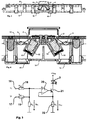
- Figures 1 and 2 show the basic structure of a device for detecting reflected and emitted light of an article 1.
- the article is a banknote.
- the object 1 is irradiated with light, which generates a lighting device 2.
- the lighting device 2 is a UV LED.
- the optical axis of the illumination device 2 is in FIG. 1 represented by an arrow 3.
- the light reflected from the surface of the article 1 is detected by a first sensor 4.
- the optical axis of the first sensor 4 is indicated by the arrow 5.
- the object 1 irradiated with the light of the illumination device 2 emits light whose wavelength differs from the incident light of the illumination device due to fluorescence and phosphorescence.
- a second sensor 6 is disposed above the article 1.
- the optical axis 7 of this second sensor 6 is perpendicular to the surface of the article 1.
- the detected by the first sensor 4 reflected light is in FIG. 1 symbolized by an arrow 8.
- the light emitted by fluorescence or phosphorescence is in FIG. 1 symbolized by the arrow 9.
- FIG. 2 shows the same schematic structure as FIG. 1 , Additionally are in FIG. 2 an optical shield 10 is shown between the illumination device 2 and the second sensor 6, and a filter 11 in front of the illumination device 2.
- the filter is a UV transmission filter which filters out the visible components of the light of the illumination device, in particular blue components .
- the second sensor 6 is an RGB sensor.
- the optical shield 10 in the form of a partition wall ensures that the UV radiation reflected directly by the object 1 does not reach the second sensor.
- FIG. 3 shows a complete device, which according to the principle FIGS. 1 and 2 is constructed.
- the device consists of two lighting devices 2, two not visible in the drawing first sensors and two second sensors 6. Both lighting devices 2 are equipped with UV-LED and a filter 11. They are each in a housing 12, which also serves as an optical shield against the two second sensors 6.
- the lighting devices 2 and the second sensors 6 are arranged on a printed circuit board 13 which is equipped with further electrical components. Printed circuit board and components arranged thereon are surrounded by a housing 14.
- the housing 14 is equipped with a protective glass 15 permeable to this light.
- FIG. 4 is the detail of the device according to FIG. 4 shown enlarged with the two illumination devices 2 and the second sensors 6.
- FIG. 5 shows a circuit diagram of the power supply of the lighting device to the device according to FIGS. 1 to 4 , Inputs 18 and 19 of a differential amplifier 20 are provided at the inputs 16 and 17 of the circuit.
- the two input resistors are connected in parallel.
- the input voltages U 1 and U 2 are generated by a digital component, not shown, for example a microcontroller, an FPGA or a CPLD.
- the differential amplifier determines the base current of a transistor 21 which is connected to the UV LED of the illumination device 2. The current through the diode is limited by a resistor 22.
- FIG. 6 a scheme of the time course of the two input voltages U 1 and U 2 is shown.
- the frequency of the input voltage U 1 is twice as large as that of the input voltage U 2 .
- the phase shift is 0.
- FIG. 7 shows that in the circuit according to FIG. 5 resulting from these input voltages time course of the current I LED of the LED of the illumination device.
- two current pulses 23 and 24 are generated.
- the current pulse 23 has a higher current than the current pulse 24.
- the duty cycle is 1/5. The strength of the current pulses and the duty cycle depend on the input voltages U 1 and U 2 and the input resistors 18 and 19.
Description
Die Erfindung geht aus von einer Vorrichtung und einem Verfahren zum Nachweis von reflektiertem und/ oder emittiertem Licht eines Gegenstandes, insbesondere eines flachen Gegenstandes.The invention is based on a device and a method for detecting reflected and / or emitted light of an object, in particular a flat object.
Derartige Vorrichtungen werden bei der Überprüfung von Gegenständen eingesetzt. Hierzu zählen das Erkennen, Kontrollieren, Verifizieren und Prüfen der Echtheit von Gegenständen und das Identifizieren von Fälschungen. Zu den Gegenständen zählen insbesondere Wertscheine oder Dokumente wie beispielsweise Banknoten, Schecks, Aktien, Papiere mit Sicherheitsaufdruck, Urkunden, Eintrittskarten oder Fahrkarten, Gutscheine, aber auch Kredit- oder Bankomatkarten, Identifikations- oder Zugangskarten. Vorrichtungen zum Nachweis von reflektiertem und/ oder emittiertem Licht eines Gegenstandes sind häufig Bestandteil eines aus mehreren Komponenten bestehenden Systems zur Be- und Verarbeitung flacher Gegenstände. Vorrichtungen zum Nachweis von reflektiertem und/ oder emittiertem Licht dienen dazu, gefälschte von echten Gegenständen zu unterscheiden. Um gefälschte von echten Gegenständen zu unterscheiden, werden die Gegenstände, insbesondere Banknoten, Sicherheits-, Ausweis- oder Wertdokumente, mit geeigneten Sicherheitsdruckfarben bedruckt. Diese vermitteln dem Betrachter im sichtbaren Spektralbereich einen bestimmten Farbeindruck. Darüber hinaus weisen sie bei Bestrahlung mit Licht im unsichtbaren Spektralbereich, beispielsweise im UV-Bereich oder im IR-Bereich, ein charakteristisches Reflexions-, Fluoreszenz- oder Phosphoreszenzverhalten auf. Da handelsübliche und gewöhnliche Druckfarben dieses Verhalten nicht zeigen, lassen sich durch die Überprüfung der Reflexion, der Fluoreszenz und der Phosphoreszenz von Licht durch Gegenstände Fälschungen von echten Gegenständen unterscheiden.Such devices are used in the inspection of objects. These include recognizing, controlling, verifying and verifying the authenticity of objects and identifying counterfeits. The items include in particular notes of value or documents such as banknotes, checks, stocks, papers with security imprint, certificates, tickets or tickets, vouchers, but also credit or debit cards, identification or access cards. Devices for detecting reflected and / or emitted light of an object are often part of a multi-component system for processing flat objects. Devices for detecting reflected and / or emitted light serve to distinguish counterfeit from real objects. In order to distinguish counterfeit from real objects, the objects, in particular banknotes, security, identity or value documents, are printed with suitable security printing inks. These give the viewer a certain color impression in the visible spectral range. In addition, when exposed to light in the invisible spectral range, for example in the UV range or in the IR range, they have a characteristic reflection, fluorescence or phosphorescence behavior. Since commercial and ordinary inks do not exhibit this behavior, checking the reflection, fluorescence, and phosphorescence of light by objects makes it possible to distinguish counterfeits from real objects.
Aus der
Aus der
In der
Als problematisch erweist sich bei der Überprüfung der Reflexion, der Fluoreszenz und der Phosphoreszenz eines Gegenstandes, dass die Intensität des durch den Gegenstand reflektierten oder emittierten Lichts entweder so hoch ist, dass der zum Nachweis eingesetzte Detektor in Sättigung geht, oder so schwach ist, dass der Detektor den Effekt nicht nachweisen kann. Da die zu überprüfenden Gegenstände Unterschiede ihrer optischen Eigenschaften, insbesondere hinsichtlich ihres Reflexions-, Fluoreszenz und Phosphoreszenzverhaltens, aufweisen, kann die Intensität des reflektierten oder emittierten Lichts nicht auf einem vorgegebenen Wert oder einen engen Bereich eingeschränkt und der Detektor oder Sensor nicht auf diesen Bereich eingestellt werden.When checking the reflection, the fluorescence and the phosphorescence of an object, it proves to be problematic that the intensity of the light reflected or emitted by the object is either so high that the detector used for detection saturates or is so weak that the detector can not detect the effect. Since the objects to be inspected have differences in their optical properties, particularly in terms of their reflection, fluorescence and phosphorescence characteristics, the intensity of the reflected or emitted light can not be limited to a predetermined value or a narrow range and the detector or sensor can not be set to this range become.
Demgegenüber weist die Vorrichtung mit den Merkmalen des Anspruchs 1 den Vorteil auf, dass sie mit einer Stromversorgung für eine Beleuchtungseinrichtung ausgestattet ist, welche die Beleuchtungseinrichtung mit einem zeitlich periodischen Strom versorgt, wobei eine Periode des zeitlichen Verlaufs mindestens zwei Strompulse mit unterschiedlichem Betrag aufweist. Die unterschiedlich starken Strompulse der Stromversorgung führen zu unterschiedlichen Intensitäten der Lichtpulse der Beleuchtungseinrichtung. Jeder Bereich des Gegenstandes wird dadurch mit einem starken und einem schwachen Lichtpuls bestrahlt. Die Frequenz des gepulsten Lichts und die zeitliche Auflösung eines Sensors, der das von dem Gegenstand reflektierte und/ oder durch Fluoreszenz und Phosphoreszenz emittierte Licht erfasst, ist dabei im Vergleich zur Geschwindigkeit der Transporteinrichtung so hoch, dass die Bewegung des Gegenstandes zwischen zwei Lichtpulsen vernachlässigbar ist. Es kann daher näherungsweise davon ausgegangen werden, dass der Gegenstand zwischen der Beleuchtung mit einem starken und einem schwachen Lichtpuls ruht.In contrast, the device with the features of
Die Sensoren erfassen das von dem Gegenstand reflektierte und/ oder emittierte Licht sowohl im Bezug auf den starken als auch im Bezug auf den schwachenThe sensors detect the light reflected and / or emitted by the object both in relation to the strong and to the weak
Lichtpuls. Wird bei dem starken Lichtpuls eine Sättigung des Sensors erreicht, so wird lediglich das reflektierte und/ oder emittierte Licht bezüglich des schwachen Lichtpulses ausgewertet. Ist dagegen das reflektierte und/ oder emittierte Licht aufgrund des schwachen Lichtpulses hinsichtlich seiner Intensität zu gering, um es mit dem Sensor nachzuweisen, so wird lediglich das reflektierte und/ oder emittierte Licht bezüglich des starken Lichtpulses ausgewertet. Auf diese Weise wird der Dynamikbereich des optischen Messsystems erweitert. Dies ermöglicht einen quantifizierten Nachweis ohne die Stärke der nachzuweisenden optischen Eigenschaften vorab zu kennen.Light pulse. If a saturation of the sensor is achieved in the strong light pulse, then only the reflected and / or emitted light is evaluated with respect to the weak light pulse. If, on the other hand, the reflected and / or emitted light is too low in its intensity due to the weak light pulse to be detected by the sensor, only the reflected and / or emitted light is evaluated with respect to the strong light pulse. In this way, the dynamic range of the optical measuring system is expanded. This allows quantified detection without knowing in advance the strength of the optical properties to be detected.
Ist die Auflösung aufgrund von zwei unterschiedlich starken Strompulsen zu gering, so kann die Anzahl der unterschiedlichen Strompulse je Periode des zeitlich periodischen Stroms erhöht werden. Die Stromstärken der Strompulse und die zeitliche Dauer der Strompulse im Verhältnis zu der Dauer der Stromstärke 0, welche als Duty Cycle bezeichnet wird, kann in Abhängigkeit von den zu untersuchenden Gegenständen vorgegeben werden. Dies gilt außerdem für die Periodendauer beziehungsweise die Frequenz des zeitlich periodischen Stroms.If the resolution is too low due to two different current pulses, the number of different current pulses per period of the time-periodic current can be increased. The current intensities of the current pulses and the duration of the current pulses in relation to the duration of the
Zeitlich periodischer Strom bedeutet in diesem Fall, dass der Strom eine periodische Funktion über der Zeit ist und damit eine Periodizität über der Zeit aufweist.Time periodic current in this case means that the current is a periodic function over time and thus has a periodicity over time.
Das erfindungsgemäße Verfahren mit den Merkmalen des Anspruchs 9 zeichnet sich dadurch aus, dass die Beleuchtungseinrichtung den Gegenstand mit gepulstem Licht bestrahlt, wobei innerhalb einer Periode des gepulsten Lichts mindestens zwei Lichtpulse unterschiedlicher Intensität erzeugt werden. Diese erfolgt dadurch, dass mittels einer Stromversorgung die Beleuchtungseinrichtung mit einem gepulsten Strom versorgt wird, wobei jede Periode mindestens zwei Strompulse mit unterschiedlicher Stromstärke aufweist. Das Verfahren kann mit der Vorrichtung gemäß Anspruch 1 durchgeführt werden.The inventive method with the features of claim 9 is characterized in that the illumination device irradiates the object with pulsed light, wherein within a period of the pulsed light at least two light pulses of different intensity are generated. This takes place in that the lighting device is supplied with a pulsed current by means of a power supply, wherein each period has at least two current pulses with different current intensity. The method can be carried out with the device according to
Nach einer vorteilhaften Ausgestaltung der Erfindung weist die Beleuchtungseinrichtung mindestens eine Licht emittierende Diode LED auf. Zwar können statt dessen auch Anregungslampen, wie beispielsweise Leuchtstofflampen und Gasentladungslampen eingesetzt werden, jedoch zeichnen sich Licht emittierende Dioden LED demgegenüber durch ein kompaktes Baumaß, einen geringeren Herstellungspreis, eine schnellere Ansprechzeit und damit eine höhere Frequenz der Lichtpulse, sowie eine geringere Stör- und Reparaturanfälligkeit aus. Von Vorteil ist in jedem Fall die Beleuchtung mit monochromatischem Licht oder zumindest Licht eines schmalen Spektralbereichs. Auf diese Weise ist eine Unterscheidung der Fluoreszenz und Phosphoreszenz von echten Gegenständen einerseits und gefälschten Gegenständen andererseits leichter möglich.According to an advantageous embodiment of the invention, the illumination device has at least one light-emitting diode LED. Although excitation lamps, such as fluorescent lamps and gas discharge lamps can be used instead, however, light emitting diodes LED are characterized by a compact dimensions, a lower manufacturing price, a faster response time and thus a higher frequency of light pulses, and a lower susceptibility to failure and repair out. The advantage in any case is the illumination with monochromatic light or at least light of a narrow spectral range. In this way it is easier to distinguish the fluorescence and phosphorescence of real objects on the one hand and counterfeit objects on the other hand.
Nach einer weiteren vorteilhaften Ausgestaltung der Erfindung ist die Licht emittierende Diode LED eine UV-Licht emittierende Diode UV-LED. UV-Licht hat den Vorteil, dass die Fluoreszenz und Phosphoreszenz im sichtbaren Spektralbereich oder nahe dem sichtbaren Spektralbereich erfolgt und daher leicht mit optischen Sensoren nachgewiesen werden kann.According to a further advantageous embodiment of the invention, the light-emitting diode LED is a UV-emitting diode UV-LED. UV light has the advantage that the fluorescence and phosphorescence takes place in the visible spectral range or near the visible spectral range and can therefore be detected easily with optical sensors.
Die Vorrichtung ist mit mindestens einem ersten Sensor zum Erfassen des von dem Gegenstand reflektierten Lichts und mit mindestens einem zweiten Sensor zum Erfassen des von dem Gegenstand durch Fluoreszenz und/ oder Phosphoreszenz emittierten Lichts ausgestattet. Der erste und der zweite Sensor befinden sich an unterschiedlichen Positionen. Bevorzugt ist die Beleuchtungseinrichtung, insbesondere die Licht emittierende Diode LED mit ihrer optischen Achse unter einem von 0° und 90° verschiedenen Winkel gegen die Transportrichtung der Transporteinrichtung angeordnet. Der erste Sensor zum Erfassen des von dem Gegenstand reflektierten Lichts ist mit seiner optischen Achse unter demselben Winkel zur Oberfläche des Gegenstandes angeordnet wie die Beleuchtungseinrichtung, allerdings symmetrisch zu einer Ebene, die senkrecht zur Oberfläche des Gegenstandes und durch den Schnittpunkt zwischen optischer Achse der Beleuchtungseinrichtung und der Oberfläche des Gegenstandes verläuft. Dabei wird ausgenutzt, dass bei der Reflexion der Einfallswinkel und Ausfallswinkel des Lichts identisch sind. Der zweite Sensor kann sich an beliebiger Position befinden, beispielsweise senkrecht über der Oberfläche des Gegenstandes. Dies bedeutet, dass seine optische Achse senkrecht zur Oberfläche des Gegenstandes ausgerichtet ist. Da die Wellenlänge des reflektierten Lichts von derjenigen des emittierten Lichts verschieden ist, werden unterschiedliche Sensoren eingesetzt. Die Wellenlänge des reflektierten Lichts stimmt mit der Wellenlänge des Lichts der Beleuchtungseinrichtung überein. Die Wellenlänge des emittierten Lichts ist geringer als diejenige des Lichts der Beleuchtungseinrichtung.The device is equipped with at least one first sensor for detecting the light reflected by the object and at least one second sensor for detecting the light emitted by the object by fluorescence and / or phosphorescence. The first and second sensors are in different positions. The illumination device, in particular the light-emitting diode LED, is preferably arranged with its optical axis at an angle other than 0 ° and 90 ° to the transport direction of the transport device. The first sensor for detecting the light reflected from the object is arranged with its optical axis at the same angle to the surface of the object as the illumination device, but symmetrical to a plane perpendicular to the surface of the object and through the intersection between optical axis of the illumination device and the surface of the object runs. It is exploited that the reflection and the angle of incidence of the light are identical in the reflection. The second sensor may be in any position, for example, vertically above the surface of the article. This means that its optical axis is aligned perpendicular to the surface of the object. Since the wavelength of the reflected light is different from that of the emitted light, different sensors are used. The wavelength of the reflected light coincides with the wavelength of the light of the illumination device. The wavelength of the emitted light is less than that of the light of the illumination device.
Nach einer weiteren vorteilhaften Ausgestaltung der Erfindung handelt es sich bei dem zweiten Sensor um einen RGB-Sensor. RGB steht dabei für die Abkürzung rot grün blau. Dieser Sensor beruht auf der Dreifarbentheorie, bei der der gesamte Farbraum aus der Überlagerung der Farben rot, grün und blau aufgebaut ist. Für jeden der drei Primärfarben wird ein eigenes Sensorelement eingesetzt.According to a further advantageous embodiment of the invention, the second sensor is an RGB sensor. RGB stands for the abbreviation red green blue. This sensor is based on the three-color theory, in which the entire color space is made up of the superimposition of the colors red, green and blue. For each of the three primary colors, a separate sensor element is used.
Nach einer weiteren vorteilhaften Ausgestaltung der Erfindung ist zwischen der Beleuchtungseinrichtung und dem zweiten Sensor eine optische Abschirmung angeordnet. Diese verhindert, dass das Licht der Beleuchtungseinrichtung zu einer Beeinträchtigung des zweiten Sensors führt. Zusätzlich dazu kann an der Beleuchtungseinrichtung ein Filter angeordnet sein, das die typischen Wellenlängen der Fluoreszenz und Phosphoreszenz aus dem Licht der Beleuchtungseinrichtung ausfiltert.According to a further advantageous embodiment of the invention, an optical shield is arranged between the illumination device and the second sensor. This prevents that the light of the illumination device leads to an impairment of the second sensor. In addition, a filter can be arranged on the illumination device, which filters out the typical wavelengths of fluorescence and phosphorescence from the light of the illumination device.
Nach einer weiteren vorteilhaften Ausgestaltung der Erfindung ist die Stromversorgung der Beleuchtungseinrichtung mit mindestens zwei parallel geschalteten Eingangswiderständen und einem Differenzverstärker ausgestattet. Ferner weist die Stromversorgung eine Spannungsquelle auf, welche mindestens zwei gepulste Eingangsspannungen liefert. Die Anzahl der gepulsten Eingangsspannungen stimmt mit der Anzahl der Strompulse je Periode der Stromversorgung überein. Bei zwei Eingangsspannungen ist die Frequenz der einen Eingangsspannung doppelt so groß wie die Frequenz der anderen Eingangsspannung. Bei einer Anzahl n an Eingangsspannungen ist die größte Frequenz das n-fache der kleinsten Frequenz. Das Maximum der Eingangsspannungen kann gleich oder verschieden sein. Die Phasenverschiebung zwischen den Eingangsspannungen beträgt 0. Durch diese besonders einfache Beschaltung mit kostengünstigen Komponenten wird in zuverlässiger Weise ein periodischer Strom mit mindestens zwei unterschiedlichen Strompulsen je Periode erzeugt.According to a further advantageous embodiment of the invention, the power supply of the illumination device is equipped with at least two input resistors connected in parallel and a differential amplifier. Furthermore, the power supply has a voltage source which supplies at least two pulsed input voltages. The number of pulsed input voltages coincides with the number of current pulses per period of the power supply. With two input voltages, the frequency of one input voltage is twice the frequency of the other input voltage. For a number n of input voltages, the largest frequency is n times the smallest frequency. The maximum of the input voltages may be the same or different. The phase shift between the input voltages is 0. This particularly simple circuit with inexpensive components reliably generates a periodic current with at least two different current pulses per period.
Die Sensoren wandeln das von dem Gegenstand reflektierte oder emittierte Licht in ein elektrisches Signal proportional zur Intensität des Lichts. Es kann sich dabei beispielsweise um Fotodioden oder CCD handeln. Dabei können mehrere derartige Komponenten in einer Zeile oder in einem Array angeordnet sein. Ferner ist der Sensor mit einem optischen System, insbesondere einem Linsensystem, ausgestattet. Darüber hinaus kann der Sensor ein Filter aufweisen, um diejenigen Wellenlängen des Lichts auszublenden, die mit dem jeweils anderen Sensor nachgewiesen werden sollen. So ist beispielsweise der zweite Sensor zum Nachweis des auf Fluoreszenz und Phosphoreszenz beruhenden Lichts mit einem Filter ausgestattet, welches das Licht im Wellenlängenbereich der Beleuchtungseinrichtung absorbiert.The sensors convert the light reflected or emitted by the article into an electrical signal proportional to the intensity of the light. It may be, for example, photodiodes or CCD. In this case, a plurality of such components can be arranged in a row or in an array. Furthermore, the sensor is equipped with an optical system, in particular a lens system. In addition, the sensor may include a filter to mask out those wavelengths of light that are to be detected with the other sensor. For example, the second sensor for detecting the light based on fluorescence and phosphorescence is equipped with a filter which absorbs the light in the wavelength range of the illumination device.
Weitere Vorteile und vorteilhafte Ausgestaltungen der Erfindung sind der nachfolgenden Beschreibung, der Zeichnung und den Ansprüchen zu entnehmen.Further advantages and advantageous embodiments of the invention will become apparent from the following description, the drawings and the claims.
In der Zeichnung ist ein Ausführungsbeispiel der erfindungsgemäßen Vorrichtung dargestellt. Es zeigen:
Figur 1- prinzipieller Aufbau der Vorrichtung,
Figur 2Vorrichtung gemäß Figur 1 mit zusätzlicher optischer Abschirmung und einem Filter,Figur 3- Längsschnitt durch eine Vorrichtung mit dem prinzipiellen Aufbau gemäß
Figur 1 - Figur 4
Detail aus Figur 3 ,Figur 5- Schaltplan zu der Vorrichtung gemäß
Figuren 1 bis 4 , Figur 6- zeitlicher Verlauf der Eingangsspannungen zum Schaltplan gemäß
Figur 5 , - Figur 7
- zeitlicher Verlauf der sich aus den beiden Eingangsspannungen gemäß
Figur 6 ergebenden Stromstärke an der UV-LED.
- FIG. 1
- basic structure of the device,
- FIG. 2
- Device according to
FIG. 1 with additional optical shielding and a filter, - FIG. 3
- Longitudinal section through a device with the basic structure according to
FIG. 1 . - FIG. 4
- Detail off
FIG. 3 . - FIG. 5
- Schematic to the device according to
FIGS. 1 to 4 . - FIG. 6
- Timing of the input voltages to the circuit diagram according to
FIG. 5 . - FIG. 7
- time course resulting from the two input voltages according to
FIG. 6 resulting amperage at the UV-LED.
In
Sämtliche Merkmale der Erfindung können sowohl einzeln als auch in beliebiger Kombination miteinander erfindungswesentlich sein.All features of the invention may be essential to the invention both individually and in any combination with each other.
- 11
- Gegenstandobject
- 22
- Beleuchtungseinrichtunglighting device
- 33
- optische Achse der Beleuchtungseinrichtungoptical axis of the illumination device
- 44
- erster Sensorfirst sensor
- 55
- optische Achse des ersten Sensorsoptical axis of the first sensor
- 66
- zweiter Sensorsecond sensor
- 77
- optische Achse des zweiten Sensorsoptical axis of the second sensor
- 88th
- von dem Gegenstand reflektiertes Lichtlight reflected from the object
- 99
- durch Fluoreszenz oder Phosphoreszenz vom dem Gegenstand emittiertes Lichtby fluorescence or phosphorescence from the light emitted by the object
- 1010
- optische Abschirmungoptical shielding
- 1111
- Filterfilter
- 1212
- Gehäuse der BeleuchtungseinrichtungHousing of the lighting device
- 1313
- Leiterplattecircuit board
- 1414
- Gehäuse der VorrichtungHousing of the device
- 1515
- Schutzglasprotective glass
- 1616
- Eingang der StromversorgungInput of the power supply
- 1717
- Eingang der StromversorgungInput of the power supply
- 1818
- Eingangswiderstandinput resistance
- 1919
- Eingangswiderstandinput resistance
- 2020
- Differenzverstärkerdifferential amplifier
- 2121
- Transistortransistor
- 2222
- Widerstandresistance
- 2323
- Strompulscurrent pulse
- 2424
- Strompulscurrent pulse
Claims (9)
- Device for the detection of reflected and/or emitted light of an object (1) when recognizing, checking, verifying and inspecting the authenticity of objects• with at least one illumination device (2), which is configured to illuminate the object (1) with pulsed light,• with at least one sensor (4, 6) having a saturation limit, which is configured to sense the light reflected and/or emitted by the object (1),• with a power supply (16, 17, 18, 19, 20, 21, 22) of the illumination device (2), which is configured to supply the illumination device (2) with a current, which is a periodic function over time, wherein one period has at least two current pulses (23, 24) of different magnitude and the differently strong current pulses of the power supply lead to different intensities of the light pulses of the illumination device, whereby each region of the object is irradiated with a first light pulse and a second light pulse, which is weaker than the first light pulse,characterized in• that it is equipped with a transport device, which is configured to transport the object relative to the illumination device (2) and past the sensor (4, 6) in a transport direction,• that it is equipped with at least one first sensor (4) for detecting the light reflected by the object (1) and at least one second sensor (6) for detecting the light emitted by the object (1) due to fluorescence and/or phosphorescence, wherein only the reflected and/or emitted light with respect to the second light pulse is evaluated, when a saturation of the respective sensor is reached during the first light pulse, and wherein only the reflected and/or emitted light with respect to the first light pulse is evaluated, when, due to the weak light pulse, the reflected and/or emitted light is to low regarding its intensity to be detected with the respective sensor, and,• that the first sensor (4) and the second sensor (6) are located at different positions.
- Device according to claim 1, characterized in that the illumination device (2) has at least one light-emitting diode.
- Device according to claim 2, characterized in that the light emitting diode is a UV light emitting diode.
- Device according to claim 1, characterized in that the first sensor (4) is oriented with its optical axis (5) at an angle of less than 90° and more than 0°, and that the second sensor (6) is oriented with its optical axis (7) at an angle of 90° regarding the transport direction of the transport device.
- Device according to claim 1 or 4, characterized in that the second sensor (6) is an RGB sensor.
- Device according to claim 1, 4 or 5, characterized in that an optical shield (10) is arranged between the illumination device (2) and the second sensor (6).
- Device according to any of the preceding claims, characterized in that the power supply for generating the time-periodic current having at least two different current pulses per period includes at least two parallel-connected input resistors (18, 19) and a differential amplifier (20).
- Device according to claim 1, characterized in that the flat object is a valued bill.
- Method for detecting reflected and/or emitted light of an object (1) during recognizing, checking, verifying and inspecting the authenticity of objects, characterized by the following method steps:• transporting the object with a transport device past at least one illumination device (2) and at least one sensor (4, 6) having a saturation limit,• supplying the illumination device (2) with a current, which is a periodic function over time, wherein one period has at least two current pulses (23, 24) of different magnitude and the differently strong current pulses of the power supply lead to different intensities of the light pulses of the illumination device,• illuminating the object (1) with the pulsed light of the illumination device (2), wherein each region of the object is irradiated with a first light pulse and a second light pulse, which is weaker than the first light pulse,• detecting the light reflected and/or emitted by the object (1) with the sensor (4, 6), wherein the light reflected from the surface of the object (1) is detected by a first sensor (4), and wherein the light emitted by the object due to fluorescence and phosphorescence is detected by a second sensor (6),• wherein only the reflected and/or emitted light with respect to the second light pulse is evaluated, when a saturation of the respective sensor is reached during the first light pulse, and wherein only the reflected and/or emitted light with respect to the first light pulse is evaluated, when, due to the weak light pulse, the reflected and/or emitted light is to low regarding its intensity to be detected with the respective sensor.
Applications Claiming Priority (2)
| Application Number | Priority Date | Filing Date | Title |
|---|---|---|---|
| DE102009005171A DE102009005171A1 (en) | 2009-01-15 | 2009-01-15 | Apparatus and method for detecting reflected and / or emitted light of an object |
| PCT/EP2009/008688 WO2010081507A1 (en) | 2009-01-15 | 2009-12-04 | Device and method for detecting reflected and/or emitted light of an object |
Publications (2)
| Publication Number | Publication Date |
|---|---|
| EP2377104A1 EP2377104A1 (en) | 2011-10-19 |
| EP2377104B1 true EP2377104B1 (en) | 2019-09-18 |
Family
ID=41682371
Family Applications (1)
| Application Number | Title | Priority Date | Filing Date |
|---|---|---|---|
| EP09801661.1A Active EP2377104B1 (en) | 2009-01-15 | 2009-12-04 | Device and method for detecting reflected and/or emitted light of an object |
Country Status (5)
| Country | Link |
|---|---|
| US (1) | US8472025B2 (en) |
| EP (1) | EP2377104B1 (en) |
| CN (1) | CN102282592B (en) |
| DE (1) | DE102009005171A1 (en) |
| WO (1) | WO2010081507A1 (en) |
Families Citing this family (9)
| Publication number | Priority date | Publication date | Assignee | Title |
|---|---|---|---|---|
| DE102009048002A1 (en) | 2009-10-02 | 2011-04-07 | Beb Industrie-Elektronik Ag | Method and device for checking the degree of soiling of banknotes |
| WO2012132011A1 (en) * | 2011-03-31 | 2012-10-04 | 富士通フロンテック株式会社 | Line sensor unit and automated transaction device |
| DE102012006347A1 (en) * | 2012-03-28 | 2013-10-02 | Brose Fahrzeugteile Gmbh & Co. Kg, Hallstadt | Method for determining distance between object e.g. person and motor vehicle e.g. car, involves receiving light reflected by object using light receiver at predetermined angle of incidence |
| CN103218870A (en) * | 2013-03-04 | 2013-07-24 | 上海古鳌电子科技股份有限公司 | Bill sorting machine capable of measuring thickness by utilizing infrared rays and carrying out authentic identification by utilizing ultraviolet rays and using method thereof |
| DE102015008409A1 (en) * | 2015-07-02 | 2017-01-05 | Eisenmann Se | Installation for optical inspection of surface areas of objects |
| US10180248B2 (en) | 2015-09-02 | 2019-01-15 | ProPhotonix Limited | LED lamp with sensing capabilities |
| DE102017008863A1 (en) | 2017-09-21 | 2018-05-30 | Daimler Ag | Method for operating an autonomously driving vehicle with a traffic-adapted driving style |
| EP3503049B1 (en) * | 2017-12-22 | 2021-02-24 | CI Tech Sensors AG | Device and method for detecting a machine-readable security feature of a valuable document |
| US11685580B2 (en) * | 2019-08-07 | 2023-06-27 | International Business Machines Corporation | Medication counterfeit detection |
Family Cites Families (29)
| Publication number | Priority date | Publication date | Assignee | Title |
|---|---|---|---|---|
| CH475600A (en) | 1967-06-15 | 1969-07-15 | Sodeco Compteurs De Geneve | Apparatus for the automatic authentication of documents, in particular banknotes, produced at least partially in steel engraving or copperplate printing |
| US4271699A (en) | 1979-12-07 | 1981-06-09 | Williamson Harry L | Sheet thickness monitoring system and method |
| EP0080309A3 (en) | 1981-11-16 | 1984-02-29 | De La Rue Systems Limited | Apparatus for analysing sheets |
| GB2170908A (en) | 1985-01-17 | 1986-08-13 | Alan Walter Sills | Sheet material thickness measuring equipment |
| JPS61138079U (en) | 1985-02-18 | 1986-08-27 | ||
| CH671754A5 (en) | 1986-09-24 | 1989-09-29 | Grapha Holding Ag | |
| GB8812893D0 (en) | 1988-05-31 | 1988-07-06 | De La Rue Syst | Apparatus for sensing sheets |
| US5226239A (en) | 1989-04-17 | 1993-07-13 | Measurex Corporation | Aerodynamic caliper gauge |
| IE914335A1 (en) | 1990-12-21 | 1992-07-01 | Measurex Corp | A sensor, system and method for determining z-directional¹properties of a sheet |
| JPH0585643A (en) | 1991-06-03 | 1993-04-06 | Fujitsu Ltd | Paper sheet thickness detection mechanism and detecting method of paper sheet thickness using same |
| GB9127112D0 (en) | 1991-12-20 | 1992-02-19 | Schlumberger Ind Ltd | Smart displacement sensor |
| GB9217568D0 (en) | 1992-08-19 | 1992-09-30 | The Technology Partnership Ltd | Device and method for detecting residual content of emptied envelopes |
| DE19841432C1 (en) | 1998-09-10 | 2000-04-20 | Siemens Nixdorf Inf Syst | Thickness examination device for sheet material |
| DE19903988B4 (en) * | 1999-02-02 | 2008-05-08 | Bundesdruckerei Gmbh | Device for the validation of authenticity features on value and security documents |
| US6360447B1 (en) | 1999-04-23 | 2002-03-26 | Agissar Corporation | Empty envelope assurance apparatus and method |
| WO2001036904A1 (en) | 1999-11-18 | 2001-05-25 | Fujitsu Limited | Pachymeter |
| DE19958048A1 (en) | 1999-12-03 | 2001-06-07 | Giesecke & Devrient Gmbh | Device and method for checking the authenticity of banknotes |
| US20050060059A1 (en) | 2003-09-15 | 2005-03-17 | Klein Robert J. | System and method for processing batches of documents |
| JP3753916B2 (en) | 2000-03-16 | 2006-03-08 | 日立オムロンターミナルソリューションズ株式会社 | Paper sheet counting device |
| GB2366371A (en) * | 2000-09-04 | 2002-03-06 | Mars Inc | Sensing documents such as currency items |
| JP2002197506A (en) * | 2000-12-26 | 2002-07-12 | Glory Ltd | Uv and fluorescence detecting device and its sensing method |
| GB0106816D0 (en) * | 2001-03-19 | 2001-05-09 | Rue De Int Ltd | Sheet handling apparatus and method |
| US6711828B2 (en) | 2001-12-05 | 2004-03-30 | First Data Corporation | Warpage measurement system and methods |
| JP3693993B2 (en) | 2002-01-28 | 2005-09-14 | 日立オムロンターミナルソリューションズ株式会社 | Paper sheet confirmation device |
| GB2404013B (en) * | 2003-07-17 | 2006-05-31 | Isis Innovation | Apparatus for and method of measuring fluorescence lifetime |
| US7131211B2 (en) | 2003-08-18 | 2006-11-07 | Micron Technology, Inc. | Method and apparatus for measurement of thickness and warpage of substrates |
| CN1270280C (en) * | 2003-12-09 | 2006-08-16 | 汤谨亮 | Popular currency examining device |
| JP4698993B2 (en) | 2004-09-15 | 2011-06-08 | 日立オムロンターミナルソリューションズ株式会社 | Thickness detector |
| EP1720135A1 (en) | 2005-05-06 | 2006-11-08 | BEB Industrie-Elektronik AG | Apparatus for measuring thickness and thickness variations |
-
2009
- 2009-01-15 DE DE102009005171A patent/DE102009005171A1/en active Pending
- 2009-12-04 CN CN200980154535.1A patent/CN102282592B/en active Active
- 2009-12-04 US US13/144,072 patent/US8472025B2/en active Active
- 2009-12-04 EP EP09801661.1A patent/EP2377104B1/en active Active
- 2009-12-04 WO PCT/EP2009/008688 patent/WO2010081507A1/en active Application Filing
Non-Patent Citations (1)
| Title |
|---|
| None * |
Also Published As
| Publication number | Publication date |
|---|---|
| US8472025B2 (en) | 2013-06-25 |
| DE102009005171A1 (en) | 2010-07-22 |
| WO2010081507A1 (en) | 2010-07-22 |
| EP2377104A1 (en) | 2011-10-19 |
| CN102282592B (en) | 2014-11-05 |
| US20110273717A1 (en) | 2011-11-10 |
| CN102282592A (en) | 2011-12-14 |
Similar Documents
| Publication | Publication Date | Title |
|---|---|---|
| EP2377104B1 (en) | Device and method for detecting reflected and/or emitted light of an object | |
| DE2320731C3 (en) | Counterfeit-proof security | |
| EP0943087B1 (en) | Device and method for detecting fluorescent and phosphorescent light | |
| DE102008050768C5 (en) | Security feature based on luminescence emitting materials, value and security document with such a security feature, a method and an apparatus for verification of such a security feature | |
| EP1245007A1 (en) | Device and method for verifying the authenticity of banknotes | |
| EP1265199A2 (en) | Device for investigating documents | |
| EP1244073A2 (en) | Method and sensor for validation of documents | |
| DE102007044878A1 (en) | Method and device for checking value documents | |
| EP1112555B1 (en) | Method and device for controlling the state of securities using a dark-field and a bright-field measurement. | |
| EP2936455B1 (en) | Sensor and method for verifying value documents | |
| DE102008047636A1 (en) | Device for authenticity examination of safety document, has sensor unit, which has suggestion module, condenser system and detector unit, where safety document is moved by sensor unit | |
| EP1265198B1 (en) | Device and method for investigating documents | |
| EP3616171B1 (en) | Method for identifying deposit material | |
| EP2453418B1 (en) | Method and device for assessing the authenticity of bank notes with security windows | |
| EP2988950B9 (en) | Calibration method and method for rapidly determining the absolute luminescence intensity | |
| WO2019242879A1 (en) | Method and sensor for testing documents | |
| DE19701513C2 (en) | Test method and test facility for authenticity control of authenticity marks | |
| DE102017008970B4 (en) | Sensor device and method for checking value documents, in particular banknotes, and value document processing system | |
| DE10259293A1 (en) | Banknote validity testing device with which luminescent light generated from security markings is detected, whereby light source and detector are arranged opposite to each other and banknotes are passed between them | |
| EP3279875B1 (en) | Pollution detector, coin sorting machine and method for contamination detection for coins | |
| DE202004019706U1 (en) | Paper currency testing machine for currency validation, has two excitation sources, receiver unit, luminescence signal evaluator and excitation source selector arranged in common housing | |
| EP2435993B1 (en) | Microsystem for recognizing predetermined features of valuable papers, security documents, or other products | |
| WO1999041710A1 (en) | Test method and device for verifying the authenticity of authenticity marks |
Legal Events
| Date | Code | Title | Description |
|---|---|---|---|
| PUAI | Public reference made under article 153(3) epc to a published international application that has entered the european phase |
Free format text: ORIGINAL CODE: 0009012 |
|
| 17P | Request for examination filed |
Effective date: 20110715 |
|
| AK | Designated contracting states |
Kind code of ref document: A1 Designated state(s): AT BE BG CH CY CZ DE DK EE ES FI FR GB GR HR HU IE IS IT LI LT LU LV MC MK MT NL NO PL PT RO SE SI SK SM TR |
|
| DAX | Request for extension of the european patent (deleted) | ||
| 17Q | First examination report despatched |
Effective date: 20141103 |
|
| STAA | Information on the status of an ep patent application or granted ep patent |
Free format text: STATUS: EXAMINATION IS IN PROGRESS |
|
| GRAP | Despatch of communication of intention to grant a patent |
Free format text: ORIGINAL CODE: EPIDOSNIGR1 |
|
| STAA | Information on the status of an ep patent application or granted ep patent |
Free format text: STATUS: GRANT OF PATENT IS INTENDED |
|
| INTG | Intention to grant announced |
Effective date: 20190412 |
|
| GRAS | Grant fee paid |
Free format text: ORIGINAL CODE: EPIDOSNIGR3 |
|
| GRAA | (expected) grant |
Free format text: ORIGINAL CODE: 0009210 |
|
| STAA | Information on the status of an ep patent application or granted ep patent |
Free format text: STATUS: THE PATENT HAS BEEN GRANTED |
|
| AK | Designated contracting states |
Kind code of ref document: B1 Designated state(s): AT BE BG CH CY CZ DE DK EE ES FI FR GB GR HR HU IE IS IT LI LT LU LV MC MK MT NL NO PL PT RO SE SI SK SM TR |
|
| REG | Reference to a national code |
Ref country code: GB Ref legal event code: FG4D Free format text: NOT ENGLISH |
|
| REG | Reference to a national code |
Ref country code: CH Ref legal event code: EP |
|
| REG | Reference to a national code |
Ref country code: DE Ref legal event code: R096 Ref document number: 502009015969 Country of ref document: DE |
|
| REG | Reference to a national code |
Ref country code: AT Ref legal event code: REF Ref document number: 1182217 Country of ref document: AT Kind code of ref document: T Effective date: 20191015 |
|
| REG | Reference to a national code |
Ref country code: IE Ref legal event code: FG4D Free format text: LANGUAGE OF EP DOCUMENT: GERMAN |
|
| RAP2 | Party data changed (patent owner data changed or rights of a patent transferred) |
Owner name: CI TECH SENSORS AG |
|
| REG | Reference to a national code |
Ref country code: DE Ref legal event code: R082 Ref document number: 502009015969 Country of ref document: DE Representative=s name: VIERING, JENTSCHURA & PARTNER MBB PATENT- UND , DE Ref country code: DE Ref legal event code: R081 Ref document number: 502009015969 Country of ref document: DE Owner name: CL TECH SENSORS AG, CH Free format text: FORMER OWNER: BEB INDUSTRIE-ELEKTRONIK AG, BURGDORF, CH |
|
| REG | Reference to a national code |
Ref country code: NL Ref legal event code: MP Effective date: 20190918 |
|
| PG25 | Lapsed in a contracting state [announced via postgrant information from national office to epo] |
Ref country code: BG Free format text: LAPSE BECAUSE OF FAILURE TO SUBMIT A TRANSLATION OF THE DESCRIPTION OR TO PAY THE FEE WITHIN THE PRESCRIBED TIME-LIMIT Effective date: 20191218 Ref country code: SE Free format text: LAPSE BECAUSE OF FAILURE TO SUBMIT A TRANSLATION OF THE DESCRIPTION OR TO PAY THE FEE WITHIN THE PRESCRIBED TIME-LIMIT Effective date: 20190918 Ref country code: NO Free format text: LAPSE BECAUSE OF FAILURE TO SUBMIT A TRANSLATION OF THE DESCRIPTION OR TO PAY THE FEE WITHIN THE PRESCRIBED TIME-LIMIT Effective date: 20191218 Ref country code: FI Free format text: LAPSE BECAUSE OF FAILURE TO SUBMIT A TRANSLATION OF THE DESCRIPTION OR TO PAY THE FEE WITHIN THE PRESCRIBED TIME-LIMIT Effective date: 20190918 Ref country code: HR Free format text: LAPSE BECAUSE OF FAILURE TO SUBMIT A TRANSLATION OF THE DESCRIPTION OR TO PAY THE FEE WITHIN THE PRESCRIBED TIME-LIMIT Effective date: 20190918 Ref country code: LT Free format text: LAPSE BECAUSE OF FAILURE TO SUBMIT A TRANSLATION OF THE DESCRIPTION OR TO PAY THE FEE WITHIN THE PRESCRIBED TIME-LIMIT Effective date: 20190918 |
|
| REG | Reference to a national code |
Ref country code: LT Ref legal event code: MG4D |
|
| PG25 | Lapsed in a contracting state [announced via postgrant information from national office to epo] |
Ref country code: GR Free format text: LAPSE BECAUSE OF FAILURE TO SUBMIT A TRANSLATION OF THE DESCRIPTION OR TO PAY THE FEE WITHIN THE PRESCRIBED TIME-LIMIT Effective date: 20191219 Ref country code: LV Free format text: LAPSE BECAUSE OF FAILURE TO SUBMIT A TRANSLATION OF THE DESCRIPTION OR TO PAY THE FEE WITHIN THE PRESCRIBED TIME-LIMIT Effective date: 20190918 |
|
| REG | Reference to a national code |
Ref country code: GB Ref legal event code: 732E Free format text: REGISTERED BETWEEN 20200206 AND 20200212 |
|
| PG25 | Lapsed in a contracting state [announced via postgrant information from national office to epo] |
Ref country code: IT Free format text: LAPSE BECAUSE OF FAILURE TO SUBMIT A TRANSLATION OF THE DESCRIPTION OR TO PAY THE FEE WITHIN THE PRESCRIBED TIME-LIMIT Effective date: 20190918 Ref country code: PL Free format text: LAPSE BECAUSE OF FAILURE TO SUBMIT A TRANSLATION OF THE DESCRIPTION OR TO PAY THE FEE WITHIN THE PRESCRIBED TIME-LIMIT Effective date: 20190918 Ref country code: PT Free format text: LAPSE BECAUSE OF FAILURE TO SUBMIT A TRANSLATION OF THE DESCRIPTION OR TO PAY THE FEE WITHIN THE PRESCRIBED TIME-LIMIT Effective date: 20200120 Ref country code: EE Free format text: LAPSE BECAUSE OF FAILURE TO SUBMIT A TRANSLATION OF THE DESCRIPTION OR TO PAY THE FEE WITHIN THE PRESCRIBED TIME-LIMIT Effective date: 20190918 Ref country code: NL Free format text: LAPSE BECAUSE OF FAILURE TO SUBMIT A TRANSLATION OF THE DESCRIPTION OR TO PAY THE FEE WITHIN THE PRESCRIBED TIME-LIMIT Effective date: 20190918 Ref country code: ES Free format text: LAPSE BECAUSE OF FAILURE TO SUBMIT A TRANSLATION OF THE DESCRIPTION OR TO PAY THE FEE WITHIN THE PRESCRIBED TIME-LIMIT Effective date: 20190918 Ref country code: RO Free format text: LAPSE BECAUSE OF FAILURE TO SUBMIT A TRANSLATION OF THE DESCRIPTION OR TO PAY THE FEE WITHIN THE PRESCRIBED TIME-LIMIT Effective date: 20190918 |
|
| PG25 | Lapsed in a contracting state [announced via postgrant information from national office to epo] |
Ref country code: CZ Free format text: LAPSE BECAUSE OF FAILURE TO SUBMIT A TRANSLATION OF THE DESCRIPTION OR TO PAY THE FEE WITHIN THE PRESCRIBED TIME-LIMIT Effective date: 20190918 Ref country code: SM Free format text: LAPSE BECAUSE OF FAILURE TO SUBMIT A TRANSLATION OF THE DESCRIPTION OR TO PAY THE FEE WITHIN THE PRESCRIBED TIME-LIMIT Effective date: 20190918 Ref country code: SK Free format text: LAPSE BECAUSE OF FAILURE TO SUBMIT A TRANSLATION OF THE DESCRIPTION OR TO PAY THE FEE WITHIN THE PRESCRIBED TIME-LIMIT Effective date: 20190918 Ref country code: IS Free format text: LAPSE BECAUSE OF FAILURE TO SUBMIT A TRANSLATION OF THE DESCRIPTION OR TO PAY THE FEE WITHIN THE PRESCRIBED TIME-LIMIT Effective date: 20200224 |
|
| REG | Reference to a national code |
Ref country code: DE Ref legal event code: R097 Ref document number: 502009015969 Country of ref document: DE |
|
| PLBE | No opposition filed within time limit |
Free format text: ORIGINAL CODE: 0009261 |
|
| STAA | Information on the status of an ep patent application or granted ep patent |
Free format text: STATUS: NO OPPOSITION FILED WITHIN TIME LIMIT |
|
| PG2D | Information on lapse in contracting state deleted |
Ref country code: IS |
|
| PG25 | Lapsed in a contracting state [announced via postgrant information from national office to epo] |
Ref country code: DK Free format text: LAPSE BECAUSE OF FAILURE TO SUBMIT A TRANSLATION OF THE DESCRIPTION OR TO PAY THE FEE WITHIN THE PRESCRIBED TIME-LIMIT Effective date: 20190918 Ref country code: IS Free format text: LAPSE BECAUSE OF FAILURE TO SUBMIT A TRANSLATION OF THE DESCRIPTION OR TO PAY THE FEE WITHIN THE PRESCRIBED TIME-LIMIT Effective date: 20200119 |
|
| 26N | No opposition filed |
Effective date: 20200619 |
|
| REG | Reference to a national code |
Ref country code: BE Ref legal event code: MM Effective date: 20191231 |
|
| PG25 | Lapsed in a contracting state [announced via postgrant information from national office to epo] |
Ref country code: SI Free format text: LAPSE BECAUSE OF FAILURE TO SUBMIT A TRANSLATION OF THE DESCRIPTION OR TO PAY THE FEE WITHIN THE PRESCRIBED TIME-LIMIT Effective date: 20190918 Ref country code: MC Free format text: LAPSE BECAUSE OF FAILURE TO SUBMIT A TRANSLATION OF THE DESCRIPTION OR TO PAY THE FEE WITHIN THE PRESCRIBED TIME-LIMIT Effective date: 20190918 |
|
| PG25 | Lapsed in a contracting state [announced via postgrant information from national office to epo] |
Ref country code: LU Free format text: LAPSE BECAUSE OF NON-PAYMENT OF DUE FEES Effective date: 20191204 Ref country code: IE Free format text: LAPSE BECAUSE OF NON-PAYMENT OF DUE FEES Effective date: 20191204 |
|
| PG25 | Lapsed in a contracting state [announced via postgrant information from national office to epo] |
Ref country code: BE Free format text: LAPSE BECAUSE OF NON-PAYMENT OF DUE FEES Effective date: 20191231 |
|
| REG | Reference to a national code |
Ref country code: AT Ref legal event code: MM01 Ref document number: 1182217 Country of ref document: AT Kind code of ref document: T Effective date: 20191204 |
|
| PG25 | Lapsed in a contracting state [announced via postgrant information from national office to epo] |
Ref country code: CY Free format text: LAPSE BECAUSE OF FAILURE TO SUBMIT A TRANSLATION OF THE DESCRIPTION OR TO PAY THE FEE WITHIN THE PRESCRIBED TIME-LIMIT Effective date: 20190918 Ref country code: AT Free format text: LAPSE BECAUSE OF NON-PAYMENT OF DUE FEES Effective date: 20191204 |
|
| PG25 | Lapsed in a contracting state [announced via postgrant information from national office to epo] |
Ref country code: HU Free format text: LAPSE BECAUSE OF FAILURE TO SUBMIT A TRANSLATION OF THE DESCRIPTION OR TO PAY THE FEE WITHIN THE PRESCRIBED TIME-LIMIT; INVALID AB INITIO Effective date: 20091204 Ref country code: MT Free format text: LAPSE BECAUSE OF FAILURE TO SUBMIT A TRANSLATION OF THE DESCRIPTION OR TO PAY THE FEE WITHIN THE PRESCRIBED TIME-LIMIT Effective date: 20190918 |
|
| PG25 | Lapsed in a contracting state [announced via postgrant information from national office to epo] |
Ref country code: TR Free format text: LAPSE BECAUSE OF FAILURE TO SUBMIT A TRANSLATION OF THE DESCRIPTION OR TO PAY THE FEE WITHIN THE PRESCRIBED TIME-LIMIT Effective date: 20190918 |
|
| PG25 | Lapsed in a contracting state [announced via postgrant information from national office to epo] |
Ref country code: MK Free format text: LAPSE BECAUSE OF FAILURE TO SUBMIT A TRANSLATION OF THE DESCRIPTION OR TO PAY THE FEE WITHIN THE PRESCRIBED TIME-LIMIT Effective date: 20190918 |
|
| PGFP | Annual fee paid to national office [announced via postgrant information from national office to epo] |
Ref country code: CH Payment date: 20230101 Year of fee payment: 14 |
|
| PGFP | Annual fee paid to national office [announced via postgrant information from national office to epo] |
Ref country code: GB Payment date: 20231121 Year of fee payment: 15 |
|
| PGFP | Annual fee paid to national office [announced via postgrant information from national office to epo] |
Ref country code: FR Payment date: 20231122 Year of fee payment: 15 Ref country code: DE Payment date: 20231121 Year of fee payment: 15 |