EP2376434B1 - Funktionelles material für gedruckte elektronische bauteile - Google Patents
Funktionelles material für gedruckte elektronische bauteile Download PDFInfo
- Publication number
- EP2376434B1 EP2376434B1 EP09799248.1A EP09799248A EP2376434B1 EP 2376434 B1 EP2376434 B1 EP 2376434B1 EP 09799248 A EP09799248 A EP 09799248A EP 2376434 B1 EP2376434 B1 EP 2376434B1
- Authority
- EP
- European Patent Office
- Prior art keywords
- oxide
- indium
- gallium
- hafnium
- magnesium
- Prior art date
- Legal status (The legal status is an assumption and is not a legal conclusion. Google has not performed a legal analysis and makes no representation as to the accuracy of the status listed.)
- Not-in-force
Links
Images



Classifications
-
- C—CHEMISTRY; METALLURGY
- C07—ORGANIC CHEMISTRY
- C07F—ACYCLIC, CARBOCYCLIC OR HETEROCYCLIC COMPOUNDS CONTAINING ELEMENTS OTHER THAN CARBON, HYDROGEN, HALOGEN, OXYGEN, NITROGEN, SULFUR, SELENIUM OR TELLURIUM
- C07F3/00—Compounds containing elements of Groups 2 or 12 of the Periodic Table
- C07F3/02—Magnesium compounds
-
- C—CHEMISTRY; METALLURGY
- C09—DYES; PAINTS; POLISHES; NATURAL RESINS; ADHESIVES; COMPOSITIONS NOT OTHERWISE PROVIDED FOR; APPLICATIONS OF MATERIALS NOT OTHERWISE PROVIDED FOR
- C09D—COATING COMPOSITIONS, e.g. PAINTS, VARNISHES OR LACQUERS; FILLING PASTES; CHEMICAL PAINT OR INK REMOVERS; INKS; CORRECTING FLUIDS; WOODSTAINS; PASTES OR SOLIDS FOR COLOURING OR PRINTING; USE OF MATERIALS THEREFOR
- C09D11/00—Inks
- C09D11/02—Printing inks
-
- H—ELECTRICITY
- H10—SEMICONDUCTOR DEVICES; ELECTRIC SOLID-STATE DEVICES NOT OTHERWISE PROVIDED FOR
- H10D—INORGANIC ELECTRIC SEMICONDUCTOR DEVICES
- H10D30/00—Field-effect transistors [FET]
- H10D30/60—Insulated-gate field-effect transistors [IGFET]
- H10D30/67—Thin-film transistors [TFT]
-
- C—CHEMISTRY; METALLURGY
- C07—ORGANIC CHEMISTRY
- C07C—ACYCLIC OR CARBOCYCLIC COMPOUNDS
- C07C249/00—Preparation of compounds containing nitrogen atoms doubly-bound to a carbon skeleton
- C07C249/04—Preparation of compounds containing nitrogen atoms doubly-bound to a carbon skeleton of oximes
- C07C249/08—Preparation of compounds containing nitrogen atoms doubly-bound to a carbon skeleton of oximes by reaction of hydroxylamines with carbonyl compounds
-
- C—CHEMISTRY; METALLURGY
- C07—ORGANIC CHEMISTRY
- C07C—ACYCLIC OR CARBOCYCLIC COMPOUNDS
- C07C251/00—Compounds containing nitrogen atoms doubly-bound to a carbon skeleton
- C07C251/32—Oximes
- C07C251/70—Metal complexes of oximes
-
- C—CHEMISTRY; METALLURGY
- C07—ORGANIC CHEMISTRY
- C07F—ACYCLIC, CARBOCYCLIC OR HETEROCYCLIC COMPOUNDS CONTAINING ELEMENTS OTHER THAN CARBON, HYDROGEN, HALOGEN, OXYGEN, NITROGEN, SULFUR, SELENIUM OR TELLURIUM
- C07F7/00—Compounds containing elements of Groups 4 or 14 of the Periodic Table
- C07F7/22—Tin compounds
- C07F7/2204—Not belonging to the groups C07F7/2208 - C07F7/2296
-
- C—CHEMISTRY; METALLURGY
- C09—DYES; PAINTS; POLISHES; NATURAL RESINS; ADHESIVES; COMPOSITIONS NOT OTHERWISE PROVIDED FOR; APPLICATIONS OF MATERIALS NOT OTHERWISE PROVIDED FOR
- C09D—COATING COMPOSITIONS, e.g. PAINTS, VARNISHES OR LACQUERS; FILLING PASTES; CHEMICAL PAINT OR INK REMOVERS; INKS; CORRECTING FLUIDS; WOODSTAINS; PASTES OR SOLIDS FOR COLOURING OR PRINTING; USE OF MATERIALS THEREFOR
- C09D11/00—Inks
- C09D11/02—Printing inks
- C09D11/03—Printing inks characterised by features other than the chemical nature of the binder
-
- C—CHEMISTRY; METALLURGY
- C09—DYES; PAINTS; POLISHES; NATURAL RESINS; ADHESIVES; COMPOSITIONS NOT OTHERWISE PROVIDED FOR; APPLICATIONS OF MATERIALS NOT OTHERWISE PROVIDED FOR
- C09D—COATING COMPOSITIONS, e.g. PAINTS, VARNISHES OR LACQUERS; FILLING PASTES; CHEMICAL PAINT OR INK REMOVERS; INKS; CORRECTING FLUIDS; WOODSTAINS; PASTES OR SOLIDS FOR COLOURING OR PRINTING; USE OF MATERIALS THEREFOR
- C09D11/00—Inks
- C09D11/30—Inkjet printing inks
-
- C—CHEMISTRY; METALLURGY
- C09—DYES; PAINTS; POLISHES; NATURAL RESINS; ADHESIVES; COMPOSITIONS NOT OTHERWISE PROVIDED FOR; APPLICATIONS OF MATERIALS NOT OTHERWISE PROVIDED FOR
- C09D—COATING COMPOSITIONS, e.g. PAINTS, VARNISHES OR LACQUERS; FILLING PASTES; CHEMICAL PAINT OR INK REMOVERS; INKS; CORRECTING FLUIDS; WOODSTAINS; PASTES OR SOLIDS FOR COLOURING OR PRINTING; USE OF MATERIALS THEREFOR
- C09D11/00—Inks
- C09D11/30—Inkjet printing inks
- C09D11/38—Inkjet printing inks characterised by non-macromolecular additives other than solvents, pigments or dyes
-
- C—CHEMISTRY; METALLURGY
- C09—DYES; PAINTS; POLISHES; NATURAL RESINS; ADHESIVES; COMPOSITIONS NOT OTHERWISE PROVIDED FOR; APPLICATIONS OF MATERIALS NOT OTHERWISE PROVIDED FOR
- C09D—COATING COMPOSITIONS, e.g. PAINTS, VARNISHES OR LACQUERS; FILLING PASTES; CHEMICAL PAINT OR INK REMOVERS; INKS; CORRECTING FLUIDS; WOODSTAINS; PASTES OR SOLIDS FOR COLOURING OR PRINTING; USE OF MATERIALS THEREFOR
- C09D11/00—Inks
- C09D11/52—Electrically conductive inks
-
- C—CHEMISTRY; METALLURGY
- C23—COATING METALLIC MATERIAL; COATING MATERIAL WITH METALLIC MATERIAL; CHEMICAL SURFACE TREATMENT; DIFFUSION TREATMENT OF METALLIC MATERIAL; COATING BY VACUUM EVAPORATION, BY SPUTTERING, BY ION IMPLANTATION OR BY CHEMICAL VAPOUR DEPOSITION, IN GENERAL; INHIBITING CORROSION OF METALLIC MATERIAL OR INCRUSTATION IN GENERAL
- C23C—COATING METALLIC MATERIAL; COATING MATERIAL WITH METALLIC MATERIAL; SURFACE TREATMENT OF METALLIC MATERIAL BY DIFFUSION INTO THE SURFACE, BY CHEMICAL CONVERSION OR SUBSTITUTION; COATING BY VACUUM EVAPORATION, BY SPUTTERING, BY ION IMPLANTATION OR BY CHEMICAL VAPOUR DEPOSITION, IN GENERAL
- C23C18/00—Chemical coating by decomposition of either liquid compounds or solutions of the coating forming compounds, without leaving reaction products of surface material in the coating; Contact plating
- C23C18/02—Chemical coating by decomposition of either liquid compounds or solutions of the coating forming compounds, without leaving reaction products of surface material in the coating; Contact plating by thermal decomposition
- C23C18/12—Chemical coating by decomposition of either liquid compounds or solutions of the coating forming compounds, without leaving reaction products of surface material in the coating; Contact plating by thermal decomposition characterised by the deposition of inorganic material other than metallic material
- C23C18/1204—Chemical coating by decomposition of either liquid compounds or solutions of the coating forming compounds, without leaving reaction products of surface material in the coating; Contact plating by thermal decomposition characterised by the deposition of inorganic material other than metallic material inorganic material, e.g. non-oxide and non-metallic such as sulfides, nitrides based compounds
- C23C18/1208—Oxides, e.g. ceramics
- C23C18/1216—Metal oxides
-
- C—CHEMISTRY; METALLURGY
- C23—COATING METALLIC MATERIAL; COATING MATERIAL WITH METALLIC MATERIAL; CHEMICAL SURFACE TREATMENT; DIFFUSION TREATMENT OF METALLIC MATERIAL; COATING BY VACUUM EVAPORATION, BY SPUTTERING, BY ION IMPLANTATION OR BY CHEMICAL VAPOUR DEPOSITION, IN GENERAL; INHIBITING CORROSION OF METALLIC MATERIAL OR INCRUSTATION IN GENERAL
- C23C—COATING METALLIC MATERIAL; COATING MATERIAL WITH METALLIC MATERIAL; SURFACE TREATMENT OF METALLIC MATERIAL BY DIFFUSION INTO THE SURFACE, BY CHEMICAL CONVERSION OR SUBSTITUTION; COATING BY VACUUM EVAPORATION, BY SPUTTERING, BY ION IMPLANTATION OR BY CHEMICAL VAPOUR DEPOSITION, IN GENERAL
- C23C18/00—Chemical coating by decomposition of either liquid compounds or solutions of the coating forming compounds, without leaving reaction products of surface material in the coating; Contact plating
- C23C18/02—Chemical coating by decomposition of either liquid compounds or solutions of the coating forming compounds, without leaving reaction products of surface material in the coating; Contact plating by thermal decomposition
- C23C18/12—Chemical coating by decomposition of either liquid compounds or solutions of the coating forming compounds, without leaving reaction products of surface material in the coating; Contact plating by thermal decomposition characterised by the deposition of inorganic material other than metallic material
- C23C18/125—Process of deposition of the inorganic material
-
- C—CHEMISTRY; METALLURGY
- C23—COATING METALLIC MATERIAL; COATING MATERIAL WITH METALLIC MATERIAL; CHEMICAL SURFACE TREATMENT; DIFFUSION TREATMENT OF METALLIC MATERIAL; COATING BY VACUUM EVAPORATION, BY SPUTTERING, BY ION IMPLANTATION OR BY CHEMICAL VAPOUR DEPOSITION, IN GENERAL; INHIBITING CORROSION OF METALLIC MATERIAL OR INCRUSTATION IN GENERAL
- C23C—COATING METALLIC MATERIAL; COATING MATERIAL WITH METALLIC MATERIAL; SURFACE TREATMENT OF METALLIC MATERIAL BY DIFFUSION INTO THE SURFACE, BY CHEMICAL CONVERSION OR SUBSTITUTION; COATING BY VACUUM EVAPORATION, BY SPUTTERING, BY ION IMPLANTATION OR BY CHEMICAL VAPOUR DEPOSITION, IN GENERAL
- C23C18/00—Chemical coating by decomposition of either liquid compounds or solutions of the coating forming compounds, without leaving reaction products of surface material in the coating; Contact plating
- C23C18/02—Chemical coating by decomposition of either liquid compounds or solutions of the coating forming compounds, without leaving reaction products of surface material in the coating; Contact plating by thermal decomposition
- C23C18/12—Chemical coating by decomposition of either liquid compounds or solutions of the coating forming compounds, without leaving reaction products of surface material in the coating; Contact plating by thermal decomposition characterised by the deposition of inorganic material other than metallic material
- C23C18/125—Process of deposition of the inorganic material
- C23C18/1279—Process of deposition of the inorganic material performed under reactive atmosphere, e.g. oxidising or reducing atmospheres
-
- C—CHEMISTRY; METALLURGY
- C23—COATING METALLIC MATERIAL; COATING MATERIAL WITH METALLIC MATERIAL; CHEMICAL SURFACE TREATMENT; DIFFUSION TREATMENT OF METALLIC MATERIAL; COATING BY VACUUM EVAPORATION, BY SPUTTERING, BY ION IMPLANTATION OR BY CHEMICAL VAPOUR DEPOSITION, IN GENERAL; INHIBITING CORROSION OF METALLIC MATERIAL OR INCRUSTATION IN GENERAL
- C23C—COATING METALLIC MATERIAL; COATING MATERIAL WITH METALLIC MATERIAL; SURFACE TREATMENT OF METALLIC MATERIAL BY DIFFUSION INTO THE SURFACE, BY CHEMICAL CONVERSION OR SUBSTITUTION; COATING BY VACUUM EVAPORATION, BY SPUTTERING, BY ION IMPLANTATION OR BY CHEMICAL VAPOUR DEPOSITION, IN GENERAL
- C23C18/00—Chemical coating by decomposition of either liquid compounds or solutions of the coating forming compounds, without leaving reaction products of surface material in the coating; Contact plating
- C23C18/02—Chemical coating by decomposition of either liquid compounds or solutions of the coating forming compounds, without leaving reaction products of surface material in the coating; Contact plating by thermal decomposition
- C23C18/12—Chemical coating by decomposition of either liquid compounds or solutions of the coating forming compounds, without leaving reaction products of surface material in the coating; Contact plating by thermal decomposition characterised by the deposition of inorganic material other than metallic material
- C23C18/125—Process of deposition of the inorganic material
- C23C18/1295—Process of deposition of the inorganic material with after-treatment of the deposited inorganic material
-
- C—CHEMISTRY; METALLURGY
- C23—COATING METALLIC MATERIAL; COATING MATERIAL WITH METALLIC MATERIAL; CHEMICAL SURFACE TREATMENT; DIFFUSION TREATMENT OF METALLIC MATERIAL; COATING BY VACUUM EVAPORATION, BY SPUTTERING, BY ION IMPLANTATION OR BY CHEMICAL VAPOUR DEPOSITION, IN GENERAL; INHIBITING CORROSION OF METALLIC MATERIAL OR INCRUSTATION IN GENERAL
- C23C—COATING METALLIC MATERIAL; COATING MATERIAL WITH METALLIC MATERIAL; SURFACE TREATMENT OF METALLIC MATERIAL BY DIFFUSION INTO THE SURFACE, BY CHEMICAL CONVERSION OR SUBSTITUTION; COATING BY VACUUM EVAPORATION, BY SPUTTERING, BY ION IMPLANTATION OR BY CHEMICAL VAPOUR DEPOSITION, IN GENERAL
- C23C18/00—Chemical coating by decomposition of either liquid compounds or solutions of the coating forming compounds, without leaving reaction products of surface material in the coating; Contact plating
- C23C18/14—Decomposition by irradiation, e.g. photolysis, particle radiation or by mixed irradiation sources
- C23C18/143—Radiation by light, e.g. photolysis or pyrolysis
-
- H—ELECTRICITY
- H10—SEMICONDUCTOR DEVICES; ELECTRIC SOLID-STATE DEVICES NOT OTHERWISE PROVIDED FOR
- H10D—INORGANIC ELECTRIC SEMICONDUCTOR DEVICES
- H10D30/00—Field-effect transistors [FET]
- H10D30/60—Insulated-gate field-effect transistors [IGFET]
- H10D30/67—Thin-film transistors [TFT]
- H10D30/6729—Thin-film transistors [TFT] characterised by the electrodes
- H10D30/6737—Thin-film transistors [TFT] characterised by the electrodes characterised by the electrode materials
- H10D30/6739—Conductor-insulator-semiconductor electrodes
-
- H—ELECTRICITY
- H10—SEMICONDUCTOR DEVICES; ELECTRIC SOLID-STATE DEVICES NOT OTHERWISE PROVIDED FOR
- H10D—INORGANIC ELECTRIC SEMICONDUCTOR DEVICES
- H10D30/00—Field-effect transistors [FET]
- H10D30/60—Insulated-gate field-effect transistors [IGFET]
- H10D30/67—Thin-film transistors [TFT]
- H10D30/674—Thin-film transistors [TFT] characterised by the active materials
- H10D30/6755—Oxide semiconductors, e.g. zinc oxide, copper aluminium oxide or cadmium stannate
-
- H—ELECTRICITY
- H10—SEMICONDUCTOR DEVICES; ELECTRIC SOLID-STATE DEVICES NOT OTHERWISE PROVIDED FOR
- H10D—INORGANIC ELECTRIC SEMICONDUCTOR DEVICES
- H10D30/00—Field-effect transistors [FET]
- H10D30/60—Insulated-gate field-effect transistors [IGFET]
- H10D30/67—Thin-film transistors [TFT]
- H10D30/6758—Thin-film transistors [TFT] characterised by the insulating substrates
-
- H—ELECTRICITY
- H10—SEMICONDUCTOR DEVICES; ELECTRIC SOLID-STATE DEVICES NOT OTHERWISE PROVIDED FOR
- H10D—INORGANIC ELECTRIC SEMICONDUCTOR DEVICES
- H10D64/00—Electrodes of devices having potential barriers
- H10D64/01—Manufacture or treatment
- H10D64/013—Manufacture or treatment of electrodes having a conductor capacitively coupled to a semiconductor by an insulator
-
- H—ELECTRICITY
- H10—SEMICONDUCTOR DEVICES; ELECTRIC SOLID-STATE DEVICES NOT OTHERWISE PROVIDED FOR
- H10D—INORGANIC ELECTRIC SEMICONDUCTOR DEVICES
- H10D64/00—Electrodes of devices having potential barriers
- H10D64/60—Electrodes characterised by their materials
- H10D64/62—Electrodes ohmically coupled to a semiconductor
-
- H—ELECTRICITY
- H10—SEMICONDUCTOR DEVICES; ELECTRIC SOLID-STATE DEVICES NOT OTHERWISE PROVIDED FOR
- H10D—INORGANIC ELECTRIC SEMICONDUCTOR DEVICES
- H10D86/00—Integrated devices formed in or on insulating or conducting substrates, e.g. formed in silicon-on-insulator [SOI] substrates or on stainless steel or glass substrates
- H10D86/40—Integrated devices formed in or on insulating or conducting substrates, e.g. formed in silicon-on-insulator [SOI] substrates or on stainless steel or glass substrates characterised by multiple TFTs
- H10D86/421—Integrated devices formed in or on insulating or conducting substrates, e.g. formed in silicon-on-insulator [SOI] substrates or on stainless steel or glass substrates characterised by multiple TFTs having a particular composition, shape or crystalline structure of the active layer
- H10D86/423—Integrated devices formed in or on insulating or conducting substrates, e.g. formed in silicon-on-insulator [SOI] substrates or on stainless steel or glass substrates characterised by multiple TFTs having a particular composition, shape or crystalline structure of the active layer comprising semiconductor materials not belonging to the Group IV, e.g. InGaZnO
-
- H—ELECTRICITY
- H10—SEMICONDUCTOR DEVICES; ELECTRIC SOLID-STATE DEVICES NOT OTHERWISE PROVIDED FOR
- H10D—INORGANIC ELECTRIC SEMICONDUCTOR DEVICES
- H10D86/00—Integrated devices formed in or on insulating or conducting substrates, e.g. formed in silicon-on-insulator [SOI] substrates or on stainless steel or glass substrates
- H10D86/40—Integrated devices formed in or on insulating or conducting substrates, e.g. formed in silicon-on-insulator [SOI] substrates or on stainless steel or glass substrates characterised by multiple TFTs
- H10D86/451—Integrated devices formed in or on insulating or conducting substrates, e.g. formed in silicon-on-insulator [SOI] substrates or on stainless steel or glass substrates characterised by multiple TFTs characterised by the compositions or shapes of the interlayer dielectrics
-
- H—ELECTRICITY
- H10—SEMICONDUCTOR DEVICES; ELECTRIC SOLID-STATE DEVICES NOT OTHERWISE PROVIDED FOR
- H10D—INORGANIC ELECTRIC SEMICONDUCTOR DEVICES
- H10D86/00—Integrated devices formed in or on insulating or conducting substrates, e.g. formed in silicon-on-insulator [SOI] substrates or on stainless steel or glass substrates
- H10D86/40—Integrated devices formed in or on insulating or conducting substrates, e.g. formed in silicon-on-insulator [SOI] substrates or on stainless steel or glass substrates characterised by multiple TFTs
- H10D86/60—Integrated devices formed in or on insulating or conducting substrates, e.g. formed in silicon-on-insulator [SOI] substrates or on stainless steel or glass substrates characterised by multiple TFTs wherein the TFTs are in active matrices
-
- H—ELECTRICITY
- H10—SEMICONDUCTOR DEVICES; ELECTRIC SOLID-STATE DEVICES NOT OTHERWISE PROVIDED FOR
- H10P—GENERIC PROCESSES OR APPARATUS FOR THE MANUFACTURE OR TREATMENT OF DEVICES COVERED BY CLASS H10
- H10P14/00—Formation of materials, e.g. in the shape of layers or pillars
- H10P14/60—Formation of materials, e.g. in the shape of layers or pillars of insulating materials
- H10P14/63—Formation of materials, e.g. in the shape of layers or pillars of insulating materials characterised by the formation processes
- H10P14/6326—Deposition processes
- H10P14/6342—Liquid deposition, e.g. spin-coating, sol-gel techniques or spray coating
- H10P14/6346—Liquid deposition, e.g. spin-coating, sol-gel techniques or spray coating using printing, e.g. ink-jet printing
-
- H—ELECTRICITY
- H10—SEMICONDUCTOR DEVICES; ELECTRIC SOLID-STATE DEVICES NOT OTHERWISE PROVIDED FOR
- H10P—GENERIC PROCESSES OR APPARATUS FOR THE MANUFACTURE OR TREATMENT OF DEVICES COVERED BY CLASS H10
- H10P14/00—Formation of materials, e.g. in the shape of layers or pillars
- H10P14/60—Formation of materials, e.g. in the shape of layers or pillars of insulating materials
- H10P14/65—Formation of materials, e.g. in the shape of layers or pillars of insulating materials characterised by treatments performed before or after the formation of the materials
- H10P14/6516—Formation of materials, e.g. in the shape of layers or pillars of insulating materials characterised by treatments performed before or after the formation of the materials of treatments performed after formation of the materials
- H10P14/6536—Formation of materials, e.g. in the shape of layers or pillars of insulating materials characterised by treatments performed before or after the formation of the materials of treatments performed after formation of the materials by exposure to radiation, e.g. visible light
- H10P14/6538—Formation of materials, e.g. in the shape of layers or pillars of insulating materials characterised by treatments performed before or after the formation of the materials of treatments performed after formation of the materials by exposure to radiation, e.g. visible light by exposure to UV light
-
- H—ELECTRICITY
- H10—SEMICONDUCTOR DEVICES; ELECTRIC SOLID-STATE DEVICES NOT OTHERWISE PROVIDED FOR
- H10P—GENERIC PROCESSES OR APPARATUS FOR THE MANUFACTURE OR TREATMENT OF DEVICES COVERED BY CLASS H10
- H10P14/00—Formation of materials, e.g. in the shape of layers or pillars
- H10P14/60—Formation of materials, e.g. in the shape of layers or pillars of insulating materials
- H10P14/69—Inorganic materials
- H10P14/692—Inorganic materials composed of oxides, glassy oxides or oxide-based glasses
- H10P14/6938—Inorganic materials composed of oxides, glassy oxides or oxide-based glasses the material containing at least one metal element, e.g. metal oxides, metal oxynitrides or metal oxycarbides
- H10P14/6939—Inorganic materials composed of oxides, glassy oxides or oxide-based glasses the material containing at least one metal element, e.g. metal oxides, metal oxynitrides or metal oxycarbides characterised by the metal
-
- H—ELECTRICITY
- H10—SEMICONDUCTOR DEVICES; ELECTRIC SOLID-STATE DEVICES NOT OTHERWISE PROVIDED FOR
- H10P—GENERIC PROCESSES OR APPARATUS FOR THE MANUFACTURE OR TREATMENT OF DEVICES COVERED BY CLASS H10
- H10P14/00—Formation of materials, e.g. in the shape of layers or pillars
- H10P14/60—Formation of materials, e.g. in the shape of layers or pillars of insulating materials
- H10P14/69—Inorganic materials
- H10P14/692—Inorganic materials composed of oxides, glassy oxides or oxide-based glasses
- H10P14/6938—Inorganic materials composed of oxides, glassy oxides or oxide-based glasses the material containing at least one metal element, e.g. metal oxides, metal oxynitrides or metal oxycarbides
- H10P14/6939—Inorganic materials composed of oxides, glassy oxides or oxide-based glasses the material containing at least one metal element, e.g. metal oxides, metal oxynitrides or metal oxycarbides characterised by the metal
- H10P14/69391—Inorganic materials composed of oxides, glassy oxides or oxide-based glasses the material containing at least one metal element, e.g. metal oxides, metal oxynitrides or metal oxycarbides characterised by the metal the material containing aluminium, e.g. Al2O3
-
- H—ELECTRICITY
- H10—SEMICONDUCTOR DEVICES; ELECTRIC SOLID-STATE DEVICES NOT OTHERWISE PROVIDED FOR
- H10P—GENERIC PROCESSES OR APPARATUS FOR THE MANUFACTURE OR TREATMENT OF DEVICES COVERED BY CLASS H10
- H10P14/00—Formation of materials, e.g. in the shape of layers or pillars
- H10P14/60—Formation of materials, e.g. in the shape of layers or pillars of insulating materials
- H10P14/69—Inorganic materials
- H10P14/692—Inorganic materials composed of oxides, glassy oxides or oxide-based glasses
- H10P14/6938—Inorganic materials composed of oxides, glassy oxides or oxide-based glasses the material containing at least one metal element, e.g. metal oxides, metal oxynitrides or metal oxycarbides
- H10P14/6939—Inorganic materials composed of oxides, glassy oxides or oxide-based glasses the material containing at least one metal element, e.g. metal oxides, metal oxynitrides or metal oxycarbides characterised by the metal
- H10P14/69392—Inorganic materials composed of oxides, glassy oxides or oxide-based glasses the material containing at least one metal element, e.g. metal oxides, metal oxynitrides or metal oxycarbides characterised by the metal the material containing hafnium, e.g. HfO2
-
- H—ELECTRICITY
- H10—SEMICONDUCTOR DEVICES; ELECTRIC SOLID-STATE DEVICES NOT OTHERWISE PROVIDED FOR
- H10P—GENERIC PROCESSES OR APPARATUS FOR THE MANUFACTURE OR TREATMENT OF DEVICES COVERED BY CLASS H10
- H10P14/00—Formation of materials, e.g. in the shape of layers or pillars
- H10P14/60—Formation of materials, e.g. in the shape of layers or pillars of insulating materials
- H10P14/69—Inorganic materials
- H10P14/692—Inorganic materials composed of oxides, glassy oxides or oxide-based glasses
- H10P14/6938—Inorganic materials composed of oxides, glassy oxides or oxide-based glasses the material containing at least one metal element, e.g. metal oxides, metal oxynitrides or metal oxycarbides
- H10P14/6939—Inorganic materials composed of oxides, glassy oxides or oxide-based glasses the material containing at least one metal element, e.g. metal oxides, metal oxynitrides or metal oxycarbides characterised by the metal
- H10P14/69395—Inorganic materials composed of oxides, glassy oxides or oxide-based glasses the material containing at least one metal element, e.g. metal oxides, metal oxynitrides or metal oxycarbides characterised by the metal the material containing zirconium, e.g. ZrO2
-
- H—ELECTRICITY
- H10—SEMICONDUCTOR DEVICES; ELECTRIC SOLID-STATE DEVICES NOT OTHERWISE PROVIDED FOR
- H10P—GENERIC PROCESSES OR APPARATUS FOR THE MANUFACTURE OR TREATMENT OF DEVICES COVERED BY CLASS H10
- H10P14/00—Formation of materials, e.g. in the shape of layers or pillars
- H10P14/60—Formation of materials, e.g. in the shape of layers or pillars of insulating materials
- H10P14/69—Inorganic materials
- H10P14/692—Inorganic materials composed of oxides, glassy oxides or oxide-based glasses
- H10P14/6938—Inorganic materials composed of oxides, glassy oxides or oxide-based glasses the material containing at least one metal element, e.g. metal oxides, metal oxynitrides or metal oxycarbides
- H10P14/6939—Inorganic materials composed of oxides, glassy oxides or oxide-based glasses the material containing at least one metal element, e.g. metal oxides, metal oxynitrides or metal oxycarbides characterised by the metal
- H10P14/69396—Inorganic materials composed of oxides, glassy oxides or oxide-based glasses the material containing at least one metal element, e.g. metal oxides, metal oxynitrides or metal oxycarbides characterised by the metal the material containing at least one rare earth metal element, e.g. oxides of lanthanides, scandium or yttrium
-
- H—ELECTRICITY
- H10—SEMICONDUCTOR DEVICES; ELECTRIC SOLID-STATE DEVICES NOT OTHERWISE PROVIDED FOR
- H10D—INORGANIC ELECTRIC SEMICONDUCTOR DEVICES
- H10D86/00—Integrated devices formed in or on insulating or conducting substrates, e.g. formed in silicon-on-insulator [SOI] substrates or on stainless steel or glass substrates
- H10D86/01—Manufacture or treatment
- H10D86/021—Manufacture or treatment of multiple TFTs
- H10D86/0241—Manufacture or treatment of multiple TFTs using liquid deposition, e.g. printing
Definitions
- the invention relates to a gallium, ruthenium, magnesium, hafnium, indium and / or tin-containing precursor for electronic components and to a production method. Furthermore, the invention relates to corresponding printed electronic components as well as suitable manufacturing methods.
- printed electronic components and systems consist of several material components, such as conductors for e.g. Contacts, semiconductors e.g. as active materials, as well as insulators e.g. as barrier layers.
- Beta-diketonates such as the acetylacetonates of zirconium and hafnium, are used in chemical vapor deposition (CVD) layer depositions.
- the compounds are evaporated in a high vacuum and deposited on heated substrates (above 500 ° C).
- heated substrates above 500 ° C.
- the conversion to the oxide ceramic takes place via several discrete intermediates, which are not used as a functional material. This high temperatures are required, which ensure a defined implementation, which prevents use in printing processes.
- ITO indium-tin-oxide
- sols of tin and indium salts in the presence of amines such as ethanolamine ( Prodi et al. Journal of Sol-Gel Science and Technology 2008, 47, 68 ).
- amines such as ethanolamine
- Zinc-tin oxide can be obtained from anhydrous stannous chloride or stannous acetate and zinc acetate hexahydrate in the presence of bases such as ethanolamine.
- the conversion to the oxide takes place, depending on the reaction procedure, on calcining at at least 350 ° C. ( D. Kim et al. Langmuir 2009, 25, 11149-11154 ) or 400-500 ° C ( SJ Seo et al. Journal of Physics D: Applied Physics, 2009, 42, 035106 ) in air.
- Indium-zinc-tin oxide is obtained from anhydrous indium chloride, zinc chloride and tin (II) chloride in ethylene glycol by reaction with sodium hydroxide solution and subsequent calcination at 600 ° C ( DH Lee et al. Journal of Materials Chemistry 2009, 19, 3135-3137 ).
- JP-B-2556317 describes halogen-containing iminoacetic acid derivatives and their metal salts, which are used for the preparation of crop protection agents.
- inorganic materials whose dielectric, semiconductive and conductive properties can be adjusted on the one hand by the material composition and on the other hand by the production method of the printed materials.
- material systems are to be developed that preserve the advantages of inorganic materials.
- the material should be able to be processed from the wet phase by a printing process. With a process step that requires only a small input of energy, the respective desired electronic performance of the material should be displayed on planar as well as flexible substrates.
- the present invention thus relates to a precursor for coating electronic components, characterized in that it contains an organometallic gallium, ruthenium, magnesium, hafnium, indium and / or tin complex and mixtures thereof containing at least one ligand from the class contains the Oximate.
- the precursors can also be prepared alkali metal-free. This can be advantageous for use in electronic components, since alkali metal-containing residues can have a negative effect on the electronic properties. These elements, as foreign atoms in the crystal, can adversely affect the properties.
- the precursor is printable and is in the form of a printing ink or printing paste for coating printed field effect transistors (FET), preferably thin film transistors (TFT).
- FET printed field effect transistors
- TFT thin film transistors
- printable precursor is to be understood as meaning a precursor material which, due to its material properties, can be processed from the wet phase by a printing process. During the printing process, a printing ink or printing paste is transported from a reservoir pressure-dependent on a substrate.
- the precursor material must be convertible into such a printing ink or printing paste, which has suitable viscosity and stability during the printing process for the printing process, as well as having suitable wettability and adhesion to the substrate.
- suitable viscosity ranges of the ink or paste are preferred for different printing processes; e.g. for inkjet printing (thermal) 1-5 mPa ⁇ s, inkjet printing (piezoelectric) 5-20 mPa ⁇ s, gravure printing 50-200 mPa ⁇ s, flexographic printing 50-500 mPa ⁇ s, screen printing 2000-40000 mPa ⁇ s ,
- the precursor contains an organometallic gallium, ruthenium, magnesium, hafnium, indium and / or tin complex with at least one ligand from the class of the oximes.
- the ligands of the gallium, ruthenium, magnesium, hafnium, indium and / or tin complex contain a 2- (methoxyimino) alkanoate, 2- (ethoxyimino) alkanoate or 2- (hydroxyimino) alkanoate.
- the ligands are synthesized by condensation of alpha-keto acids or oxocarboxylic acids with hydroxylamines or alkylhydroxylamines in the presence of bases in aqueous or methanolic solution.
- the precursors or gallium, ruthenium, magnesium, hafnium, indium and / or tin complexes are formed at room temperature by reacting an oxocarboxylic acid with at least one hydroxyl or alkylhydroxylamine in the presence of a base, such as tetraethylammonium bicarbonate or sodium bicarbonate and subsequent addition an inorganic gallium, ruthenium, magnesium, hafnium, indium and / or tin salt such as Gallium nitrate hexahydrate, ruthenium trichloride hexahydrate, magnesium nitrate hexahydrate, hafnium oxochloride octahydrate, anhydrous indium chloride and / or stannous chloride pentahydrate.
- a base such as tetraethylammonium bicarbonate or sodium bicarbonate
- an oxcarboxylic acid may be reacted in the presence of at least one hydroxyl or alkylhydroxylamine with a hydroxocarbonate of magnesium or hafnium, such as hydromagnesite Mg 5 (CO 3 ) 4 (OH) 2 .4H 2 O.
- a hydroxocarbonate of magnesium or hafnium such as hydromagnesite Mg 5 (CO 3 ) 4 (OH) 2 .4H 2 O.
- hydroxocarboxylic acid all representatives of this class of compounds can be used. However, preference is given to using oxoacetic acid, oxopropionic acid or oxobutyric acid.
- the thermal transformation of the gallium, magnesium or hafnium complex precursor into the functional gallium oxide, magnesium oxide or hafnium oxide layer with insulating properties or of the ruthenium complex precursor in a layer of ruthenium oxide takes place at a temperature ⁇ 80 ° C.
- the temperature is between 150 and 200 ° C.
- the thermal conversion of the indium and tin complex precursors into the functional indium tin oxide layer with conductive properties takes place at a temperature ⁇ 150 ° C.
- the temperature is between 150 and 250 ° C.
- the thermal conversion of the indium, gallium and zinc complex precursors into the functional indium gallium zinc oxide layer with semiconducting properties takes place at a temperature ⁇ 150 ° C.
- the temperature is between 150 and 250 ° C.
- the thermal conversion of the zinc and tin complex precursors into the functional zinc-tin oxide layer with semiconducting properties takes place at a temperature ⁇ 150 ° C.
- the temperature is between 150 and 250 ° C.
- the conversion of the gallium, magnesium or hafnium complex precursor into the functional gallium, magnesium or hafnium oxide layer with insulating properties or the conversion of the ruthenium complex precursor into ruthenium oxide or the conversion of indium and tin complex precursors in the functional indium tin oxide layer having conductive properties or the conversion of the indium gallium zinc and tin complex precursors in the functional oxide layer having semiconducting properties is carried out in a further preferred embodiment by irradiation with UV light having wavelengths ⁇ 400 nm Wavelength between 150 and 380 nm.
- the advantage of the UV irradiation is that the resulting gallium oxide, ruthenium oxide, magnesium oxide, hafnium oxide, indium tin oxide and indium gallium zinc oxide or zinc tin oxide layers have a lower surface roughness exhibit. Namely, an increased roughness of the surfaces would mean, for the thin subsequent layers, an increased risk that these layers can not be formed homogeneously and thus are not electrically functional (for example short circuit due to a defective dielectric layer).
- Aluminum oxide, gallium oxide, neodymium oxide, magnesium oxide, hafnium oxide or zirconium oxide layers which are produced from the corresponding precursors, show a breakdown voltage between two conductors> 0.1 MV / cm. Preferably, breakdown voltages between 1 and 10 MV / cm. The breakdown voltage can be determined by means of the measuring and evaluation methods described in DIN EN ISO 2376: 2009-07.
- the indium-tin oxide layer has a resistivity (determined by four-point measurement) of ⁇ 10 -3 Ohm-cm.
- resistivities are between 10 -3 and 10 -5 ohm.cm.
- the conductivity can be determined by means of four-probe DC methods. This measuring method is described in DIN 50431 or ASTM F43-99.
- the indium-gallium-zinc oxide layers (IGZO) or the zinc-tin oxide layers (ZTO) have a charge carrier mobility> 10 -3 cm 2 / Vs.
- Charge carrier mobilities of 0.1 to 10 cm 2 / Vs are preferred.
- Another object of the present invention is the use of an organometallic aluminum, gallium, neodymium-ruthenium, magnesium, hafnium, zirconium, indium and / or tin complex or precursor for producing one or more functional layers in the field effect transistor.
- the substrate can be both a solid substrate such as glass, ceramic, metal or a plastic substrate and also a flexible substrate, in particular plastic film or metal foil.
- a flexible substrate film is used according to the invention.
- Preferred according to the invention is the TFT, with which large-area electronic circuits can be produced.
- the aluminum, gallium, neodymium, magnesium, hafnium or zirconium oxide layer has a thickness of 15 nm to 1 .mu.m, preferably 30 nm to 750 nm.
- the layer thickness depends on the particular coating technology used and its parameters , In the case of spin coating, these are, for example, the rotation speed and duration.
- the indium-tin-oxide layer has a thickness of 15 nm to 1 .mu.m, preferably 100 nm to 500 nm.
- the layer thickness depends on the particular coating technique used and its parameters. in the In the case of spin coating, these are, for example, the rotation speed and duration.
- the indium-gallium-zinc oxide (IGZO) or zinc-tin oxide (ZTO) layer has a thickness of 15 nm to 1 .mu.m, preferably 20 nm to 200 nm.
- the layer thickness depends on the particular coating technique used and its parameters. In the case of spin coating, these are, for example, the rotation speed and duration.
- the aforementioned electronic components consist of a field-effect transistor or thin-film transistor, which is composed of a gate, an insulating layer, a semiconductor and electrodes (drain and source).
- the gate preferably consists of a highly n-doped silicon wafer, a highly n-doped silicon thin film, conductive polymers (eg polypyrrolepolyaminobenzenesulfonic acid or polyethylenedioxythiophene-polystyrenesulfonic acid (PEDOT-PSS)), conductive ceramics (eg indium-tin-oxide (ITO) or Al, Ga or In-doped tin oxide (AZO, GZO, IZO) as well as F or Sb doped tin oxide (FTO, ATO)) or metals (eg gold, silver, titanium, zinc), depending on the design as a thin layer or substrate material.
- conductive polymers eg polypyrrolepolyaminobenzenesulfonic acid
- the thin layers may be applied in the arrangement below (bottom gate) or above (top gate) the semiconducting or insulating layer.
- the electronic component preferably has an insulating layer which consists of polymers (for example poly (4-vinylphenol), polymethyl methacrylate, polystyrene, polyimides or polycarbonate) or ceramics (for example silicon dioxide, silicon nitride, aluminum oxide, gallium oxide, neodymium oxide, magnesium oxide, hafnium oxide, zirconium oxide).
- the electronic device has a semiconductive layer composed of a semiconducting organic compound (e.g., polythiophene, oligothiophene, or polytriarylamine) or ceramics (e.g., zinc oxide, indium-gallium-zinc oxide (IGZO), or zinc-tin oxide (ZTO)).
- a semiconducting organic compound e.g., polythiophene, oligothiophene, or polytriarylamine
- ceramics e.g., zinc oxide, indium-gallium-zinc oxide (IGZO), or zinc-tin oxide (ZTO)
- the electronic component preferably has source and drain electrodes made of a highly n-doped silicon thin film, conductive polymers (eg polypyrrole-polyaminobenzenesulfonic acid or polyethylenedioxythiophene-polystyrenesulfonic acid (PEDOT-PSS)), conductive ceramics (eg indium tin oxide (ITO) or Al, Ga or In-doped tin oxide (AZO, GZO, IZO) and F or Sb-doped tin oxide (FTO, ATO)) or metals (eg gold, silver, titanium, zinc).
- the electrodes preferably designed as thin layers according to the invention
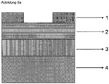
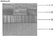
- the electrodes can be applied depending on the design in the arrangement below (bottom contact) or above (top contact) of the semiconducting or the insulating layer (see Figure 8a and b ).
- gate, insulator and semiconductor may be deposited unstructured by spin coating or dipcoating, as well as gaseous or liquid phase deposition techniques.
- Next can be gate, insulator, semiconductors and Electrodes structured by flexo / gravure printing, inkjet printing and deposition techniques from the gaseous or liquid phase can be applied. According to the invention, printing methods are preferred.
- This method produces both electronic components and the connections of individual components in integrated circuits.
- Example 2 Alkali metal-free preparation of the magnesium oxide precursor bis [2- (methoxyimino) propanoato] magnesium
- Example 3 Production of undoped magnesium oxide layers from the magnesium precursor with insulator properties (from Example 1 or 2)
- the magnesium oximat prepared according to Example 1 or 2 is applied to a substrate made of glass, ceramic or polymer by means of spin coating (or dipcoating or else inkjet printing). It is then annealed in air at temperatures above 210 ° C for 10 minutes.
- the magnesium oxide films thus obtained exhibit a uniform, crack-free, non-porous surface morphology.
- the layers consist of amorphous or nanocrystalline material. The layers have insulator properties.
- Example 4 Preparation of a zirconium dioxide precursor zirconium hydroxo [2- (methoxyimino) propanoate], Comparative Example
- the residue is taken up in 100 ml of dichloromethane and the resulting suspension is filtered again.
- the product is then precipitated from the filtrate with plenty of n-hexane, filtered off and dried in a desiccator. Yield 3.50 g.
- the compound thus obtained can be characterized by IR and NMR spectroscopy.
- Example 5 Preparation of zirconium oxide layers from the zirconium dioxide precursor
- the zirconium oxime prepared according to Example 4 is applied to a substrate made of glass, ceramic or polymer by means of spincoating (or dipcoating or else inkjet printing). Subsequently, in the air at temperatures above 200 ° C for 10 minutes annealed or UV irradiation with 150 mW / cm 2 carried out for 15 minutes.
- the zirconia films thus obtained exhibit a uniform, crack-free, non-porous surface morphology.
- the layers consist of amorphous or nanocrystalline material. The layers have insulator properties.
- the hafnium oxime prepared according to Example 6 is applied by spin coating (or dip coating or inkjet printing) to a substrate made of glass, ceramic or polymer. Subsequently, in the air at temperatures above 200 ° C for 10 minutes annealed or UV irradiation with 150 mW / cm 2 carried out for 15 minutes.
- the hafnium oxide films thus obtained exhibit a uniform, crack-free, non-porous surface morphology.
- the layers consist of amorphous or nanocrystalline material. The layers have insulator properties.
- Example 9 Preparation of alumina layers with insulator properties
- the Aluminiumoximat prepared according to Example 8 is applied by spin coating (or dip coating or inkjet printing) to a substrate made of glass, ceramic or polymer. Then it is added in the air Temperatures above 200 ° C annealed for 10 minutes or UV irradiation with 150 mW / cm 2 carried out for 15 minutes.
- the resulting alumina films exhibit a uniform, crack-free, non-porous surface morphology.
- the layers consist of nanocrystalline material.
- the layers have insulator properties.
- Example 11 Preparation of gallium oxide layers with insulator properties
- the gallium oximate produced according to Example 10 is applied to a substrate made of glass, ceramic or polymer by means of spin coating (or dipcoating or else inkjet printing). Subsequently, in the air at temperatures above 200 ° C for 10 minutes annealed or UV irradiation with 150 mW / cm 2 carried out for 15 minutes.
- the gallium oxide films thus obtained show a uniform, crack-free, non-porous Surface morphology.
- the layers consist of nanocrystalline material. The layers have insulator properties.
- Example 12 Preparation of a neodymium oxide precursor Tris [2- (methoxyimino) propanoato] neodymium, comparative example
- Example 13 Preparation of neodymium oxide layers with insulator properties
- the neodymium oxime produced according to Example 12 is applied to a substrate made of glass, ceramic or polymer by means of spin coating (or dipcoating or else inkjet printing). Subsequently, in the air at temperatures above 200 ° C for 10 minutes annealed or UV irradiation with 150 mW / cm 2 carried out for 15 minutes.
- the neodymium oxide films thus obtained exhibit a uniform, crack-free, non-porous surface morphology.
- the layers consist of nanocrystalline material. The layers have insulator properties.
- the Rutheniumoximat prepared according to Example 14 is applied by spin coating (or dip coating or inkjet printing) to a substrate made of glass, ceramic or polymer. Subsequently, in the air at temperatures above 200 ° C for 10 minutes annealed or UV irradiation with 150 mW / cm 2 carried out for 15 minutes.
- the resulting ruthenium oxide films exhibit a uniform, crack-free, non-porous surface morphology. Depending on the calcination temperature, the layers consist of nanocrystalline material.
- the example shows the production of a dielectric layer.
- a layer of zirconia is deposited by spin coating or printing and presented by subsequent calcination at 200 ° C for 10 minutes or UV irradiation at 150 mW / cm 2 for 15 minutes.
- the breakdown voltage for the dielectric layer can be determined to be 1 MV / cm.
- the example shows a field effect transistor (FET) according to Figures 8a and 8b.
- the device consists of a highly n-doped silicon wafer, on which the dielectric layer is applied.
- a semiconducting layer is shown, followed by an electrode structure made of metal, which is produced by vapor deposition of the metal or printing of a metal ink ( Figure 8a ).
- Figure 8b first the production of the electrode structure and then the application of the semiconductor layer can take place.
- the product is then precipitated from the filtrate with plenty of n-hexane, filtered off and dried in a desiccator. Yield 1.80 g (58.9%).
- the compound thus obtained can be characterized by IR and NMR spectroscopy.
- the residue is taken up in 100 ml of acetone or dimethoxyethane and the resulting suspension is filtered again.
- the product from the filtrate is precipitated with plenty of diethyl ether, filtered off and dried in a desiccator. Yield 3.7 g.
- the compound thus obtained can be characterized by IR and NMR spectroscopy.
- Example 20 Preparation of electrically conductive layers of indium tin oxide (ITO)
- the indium and Zinnoximate prepared according to Example 18 and 19 are brought together in a molar ratio of 90:10 in solution and applied by spin coating (or dip coating or inkjet printing) to a substrate made of glass, ceramic or polymer.
- the mixture is then tempered in air at temperatures above 200 ° C for 60 minutes or UV irradiation with 150 mW / cm 2 for 1 hour.
- the indium-tin oxide films thus obtained show a uniform, crack-free, non-porous Surface morphology.
- the layers consist of amorphous or nanocrystalline material.
- the layers have electrical conductivity.
- Example 21 Preparation of semiconductive layers of indium-gallium-zinc oxide (IGZO)
- indium and / or gallium oximes prepared according to Examples 10 and 18, as well as zinc oximes are dissolved in a suitable molar ratio.
- the solution thus obtained is applied by spin coating (or dipcoating or inkjet printing) to a substrate made of glass, ceramic or polymer.
- the mixture is then heated or air at temperatures above 200 ° C for 10 minutes of UV irradiation of 150 mW / cm 2 was carried out for 15 minutes.
- the indium-gallium-zinc oxide films thus obtained exhibit a uniform, crack-free, non-porous surface morphology.
- the layers are made of amorphous material. The layers have semiconducting properties.
- Example 22 Preparation of Semi-conductive Coatings from Zinc-Tin Oxide (ZTO)
- the tin oximes and zinc oximes prepared according to Example 19 are dissolved together in an appropriate ratio.
- tin contents Sn / (Sn + Zn) of 0 to 30 mole percent are suitable.
- the solution is applied to a glass, ceramic or polymer substrate by spin coating (or dipcoating, or else inkjet printing). Subsequently, in air at temperatures above 200 ° C annealed for 10 minutes or UV irradiation at 150 mW / cm 2 for 15 minutes.
- the resulting zinc-tin oxide films show a uniform, crack-free, non-porous surface morphology.
- the layers consist of amorphous or nanocrystalline material. The layers have semiconducting properties.
- Suitable solvents are 2-methoxyethanol, 2-butanol, methanol, dimethylformamide or mixtures thereof.
- the viscosity of the printing inks can be determined using a rheometer, eg MARS Rheometer from Haake. The determination is carried out under standard conditions (DIN 50 014-23).
Landscapes
- Chemical & Material Sciences (AREA)
- Organic Chemistry (AREA)
- Engineering & Computer Science (AREA)
- Materials Engineering (AREA)
- Chemical Kinetics & Catalysis (AREA)
- General Chemical & Material Sciences (AREA)
- Mechanical Engineering (AREA)
- Metallurgy (AREA)
- Inorganic Chemistry (AREA)
- Thermal Sciences (AREA)
- Physics & Mathematics (AREA)
- Wood Science & Technology (AREA)
- Life Sciences & Earth Sciences (AREA)
- Ceramic Engineering (AREA)
- Toxicology (AREA)
- Health & Medical Sciences (AREA)
- Thin Film Transistor (AREA)
- Parts Printed On Printed Circuit Boards (AREA)
- Organic Low-Molecular-Weight Compounds And Preparation Thereof (AREA)
- Non-Metallic Protective Coatings For Printed Circuits (AREA)
Description
- Die Erfindung betrifft einen Gallium-, Ruthenium-, Magnesium-, Hafnium-, Indium- und/oder Zinn-haltigen Precursor für elektronische Bauteile sowie ein Herstellverfahren. Des Weiteren betrifft die Erfindung entsprechende gedruckte elektronische Bauelemente sowie dazu geeignete Herstellverfahren.
- Für den Einsatz gedruckter Elektronik in Massenanwendungen (z.B. RFID (=Radio Frequency Identification) Chips auf Einzelverpackungen) ist die Verwendung von etablierten Massendruckverfahren wünschenswert. Generell bestehen gedruckte elektronische Bauteile und Systeme aus mehreren Materialkomponenten, wie Leiter für z.B. Kontaktierungen, Halbleiter z.B. als aktive Materialien, sowie Isolatoren z.B. als Sperrschichten.
- Die Verfahren zur Herstellung bestehen zumeist aus einem Depositionsschritt, also dem Aufbringens des jeweiligen Materials auf ein Trägermaterial (Substrat), sowie aus einem darauf folgenden Prozessschritt, der die gewünschten Eigenschaften des Materials sicherstellt. Wünschenswert im Hinblick auf eine massentaugliche z.B. Rolle-zu-Rolle Verarbeitung ist die Verwendung flexibler Substrate (Folien). Bisherige Verfahren zur Herstellung gedruckter Schaltungen weisen intrinsische Vor- aber auch Nachteile auf:
- Konventionelle Technologie siehe
WO 2004086289 ): Hier werden Hybride aus konventionellen Si-Logikbaustein und zusätzlicher strukturierter oder gedruckter Komponenten (z.B. Metallantenne im Falle RFID Chip) kostenintensiv zusammengefügt. Dieses Verfahren wird jedoch als zu aufwändig im Hinblick auf eine reale Volumenanwendung gesehen. - Organische Materialien (siehe
DE 19851703 ,WO 2004063806 ,WO 2002015264 ): Bei diesen Systemen handelt es sich um gedruckte Elektronikkomponenten auf Basis von Polymeren aus der flüssigen Phase. Diese Systeme zeichnen sich durch eine im Vergleich zu den vorher genannten Materialien (konventionelle Technologie) einfache Verarbeitung aus Lösungen aus. Als Prozessschritt ist hierbei nur die Trocknung des Lösungsmittels zu berücksichtigen. Allerdings ist die erreichbare Leistungsfähigkeit im Falle z.B. halbleitender oder leitender Materialien durch limitierende materialtypische Eigenschaften, wie z.B. der Ladungsträgerbeweglichkeit <10 cm2 /Vs durch sog. Hopping-Mechanismen, beschränkt. Diese Beschränkung wirkt sich auf die Anwendungsmöglichkeiten aus: die Leitungsfähigkeit eines gedruckten Transistors erhöht sich mit reduzierter Ausdehnung des halbleitenden Kanals, der derzeit mit Massenverfahren nicht kleiner als ∼ 40 µm gedruckt werden kann. Eine weitere Beschränkung der Technologie stellt die Empfindlichkeit der organischen Komponenten gegenüber Umgebungsbedingungen dar. Diese bewirkt eine aufwändige Prozessführung während der Herstellung sowie gegebenenfalls eine verkürzte Lebensdauer der gedruckten Komponenten. - Anorganische Materialien: diese Materialklasse hat generell durch unterschiedliche intrinsische Eigenschaften (z.B. Stabilität gegen UVbedingten Abbau) im Vergleich zu den organischen Materialien das Potential für eine erhöhte Leistungsfähigkeit bei Verwendung in gedruckter Elektronik.
- i) Präparation aus der Gasphase ohne zusätzlichen Prozessschritt: in diesem Fall ist es möglich, sehr gut isolierende dünne Schichten zu erzeugen, allerdings limitiert die damit verbundene kostenintensive Vakuumtechnologie sowie das langsame Schichtwachstum eine Anwendung im Massenmarkt.
- ii) Nasschemische Herstellung ausgehend von Precursormaterialien, wobei die Materialien aus der flüssigen Phase z.B. durch Aufschleudern oder Drucken aufgebracht werden (siehe
US 6867081 ,US 6867422 ,US 2005/0009225 ). Teilweise werden auch Mischungen von anorganischen Materialien und organischer Matrix verwendet (sieheUS 2006/0014365 ) Um eine durchgehende elektrische Eigenschaft der hergestellten Schicht zu gewährleisten, ist zumeist ein Prozessschritt erforderlich, der über ein Verdampfen des Lösungsmittels hinausgeht. In allen Fällen muss eine Morphologie mit ineinander übergehenden Bereichen erzeugt werden, wobei Precursoren aus der Nassphase zusätzlich in das gewünschte aktive Material überführt werden. Dadurch wird eine gewünschte Funktionalität erzeugt (im Falle von Halbleitern: hohe Ladungsträgerbeweglichkeit). Die Prozessierung erfolgt daher bei Temperaturen > 300°C, was allerdings eine Verwendung dieses Prozesses zur Folienbeschichtung verhindert. - Beispiele für die Verwendung eines Vorläufer- bzw. Precursormaterials für MgO wird z.B. in Stryckmans et al. Thin Solid Films 1996, 283, 17 (aus Magnesiumacetylacetonat oberhalb 260°C) oder Raj et al. Crystal Research and Technology 2007, 42, 867 (aus Magnesiumacetat ab 300°C in mehreren Stufen) beschrieben. In beiden Fällen wird dort zur Schichtabscheidung aus der Gasphase die Spray-Pyrolyse eingesetzt. Dabei werden die Lösungen auf ein aufgeheiztes Substrat (oberhalb 400°C) aufgespritzt und gegebenenfalls bei noch höherer Temperatur nachbehandelt. Die erforderlichen hohen Temperaturen verhindern eine Verwendung in Druckprozessen.
- Ein Beispiel für die Verwendung eines löslichen ZrO2- Precursormaterials wird in Ismail et al. Powder Technology 1995, 85, 253 (aus Zirkoniumacetylacetonat über mehrere Stufen zwischen 200 bis 600 °C) beschrieben.
- Ein Beispiel für die Verwendung eines löslichen HfO2 ist z.B. aus Zherikova et al. Journal of Thermal Analysis and Calorimetry 2008, 92, 729 (aus Hafniumacetylacetonat über mehrere Stunden zwischen T = 150 und 500°C) bekannt.
- Beta-Diketonate, wie die Acetylacetonate von Zirkonium und Hafnium, werden in Schichtabscheidungen aus der Gasphase mittels Chemical Vapour Deposition (CVD) eingesetzt. Dabei werden die Verbindungen im Hochvakuum verdampft und auf aufgeheizten Substraten (oberhalb von 500°C) abgeschieden. Die Umwandlung zur oxidischen Keramik erfolgt über mehrere diskrete Zwischenstufen, die aber nicht als funktionales Material Verwendung finden. Damit sind hohe Temperaturen erforderlich, die eine definierte Umsetzung gewährleisten, was eine Verwendung in Druckprozessen verhindert.
- Zur Herstellung von Indium-Zinn-Oxid (abgekürzt: "ITO" genannt) werden als Vorläufer beispielsweise Sole aus Zinn- und Indiumsalzen in Gegenwart von Aminen wie Ethanolamin verwendet (Prodi et al. Journal of Sol-Gel Science and Technology 2008, 47, 68). Die Umwandlung zum Oxid erfolgt hier bei Temperaturen oberhalb von 500-600°C. Die erforderlichen hohen Temperaturen verhindern eine Verwendung in Druckprozessen auf temperaturempfindlichen Substraten.
- Von Interesse ist die Herstellung amorpher, halbleitender Oxidkeramiken (K. Nomura et al. Nature 2004, 432, 488-492; H.Hosono Journal of Non-Crystalline Solids 2006, 352, 851-858; T. Kamiya et al. Journal of Display Technology 2009, 5, 273-288). Dabei ist das Phasensystem Indium-Gallium-Zinn-Zink-Sauerstoff eingehend untersucht worden. Typische Beispiele sind Indium-Gallium-Zinkoxid (abgekürzt "IGZO"), sowie Zink-Zinnoxid (abgekürzt "ZTO"), aber auch Indium-Zink-Zinnoxid (abgekürzt "IZTO").
- Die Abscheidung der halbleitenden Schichten erfolgt zumeist über die Gasphase, aber auch auf Lösungen basierende Prozesse sind bekannt. Die dabei eingesetzten Sole machen jedoch höhere Prozessierungstemperaturen erforderlich. Zink-Zinnoxid kann aus wasserfreiem Zinn(II)chlorid oder Zinn(II)acetat und Zinkacetathexahydrat in Gegenwart von Basen wie Ethanolamin erhalten werden. Die Umwandlung zum Oxid (unter Oxidation der Zinnkomponenten) erfolgt in Abhängigkeit von der Reaktionsführung bei Calcinierung bei mindestens 350°C (D. Kim et al. Langmuir 2009, 25, 11149-11154) oder 400-500°C (S.J. Seo et al. Journal of Physics D: Applied Physics, 2009, 42, 035106) an Luft. Indium-Zink-Zinnoxid wird aus wasserfreiem Indiumchlorid, Zinkchlorid und Zinn(II)chlorid in Ethylenglykol durch Reaktion mit Natronlauge und nachfolgender Calcinierung bei 600°C erhalten (D.H. Lee et al. Journal of Materials Chemistry 2009, 19, 3135-3137).
- Aus M. R. Hill et. al., Inorganica Chimica Acta 358 (2005) 201 - 206 ist die Verwendung von Zink-Ketoacidooximaten zur Herstellung von Zinkoxid mit Hilfe eines CVD-Verfahrens bekannt.
- Der Einsatz dieser herkömmlichen Precursoren zur Herstellung gedruckter Schaltungen ist in ihrer Anwendbarkeit in der Volumenproduktion einer Massendruckanwendung beschränkt.
- In A. W. Apblett et. al., Mat. Res. Soc. Symp. Proc. Vol 294 (1993) 123 - 128, sind Brenztraubensäure-Metalloximate verschiedener Metalle beschrieben, die sich zur Herstellung spezieller Keramiken eignen, in denen radioaktiver Abfall gebunden werden soll.
-
JP-B-2556317 - Aufgabe der vorliegenden Erfindung war es daher, anorganische Materialien zur Verfügung zu stellen, deren dielektrische, halbleitende sowie leitende Eigenschaften einerseits durch die Materialzusammensetzung und andererseits durch das Herstellverfahren der gedruckten Materialien einstellbar sind. Dazu sollen Materialsysteme entwickelt werden, die die Vorteile anorganischer Materialien bewahren. Das Material soll aus der Nassphase durch ein Druckverfahren verarbeitet werden können. Mit einem Verfahrensschritt, der nur einen geringen Energieeintrag erfordert, soll die jeweils gewünschte elektronische Leistungsfähigkeit des Materials auf planaren, sowie flexiblen Substraten dargestellt werden.
- Jetzt wurde überraschend ein Verfahren entwickelt, bei dem ein neuartiges metallorganisches Precursormaterial hergestellt, auf Oberflächen aufgebracht und im Anschluss daran bei niedrigen Temperaturen in ein dielektrisch aktives, d.h. isolierendes sowie auch in ein elektrisch halbleitendes oder leitendes Material umgewandelt wird. Die dabei erzeugten Schichten zeichnen sich durch Oberflächeneigenschaften aus, die für einen Druckprozess vorteilhaft sind.
- Gegenstand der vorliegenden Erfindung ist somit ein Precursor zum Beschichten von elektronischen Bauteilen, gekennzeichnet dadurch, dass er einen metallorganischen Gallium-, Ruthenium-, Magnesium-, Hafnium- Indium- und/oder Zinnkomplex sowie deren Gemische enthält, der mindestens einen Liganden aus der Klasse der Oximate enthält.
- Bei geeigneter Reaktionsführung können die Precursoren auch alkalimetallfrei hergestellt werden. Dies kann für den Einsatz in elektronischen Bauteilen vorteilhaft sein, da sich alkalimetallhaltige Rückstände negativ auf die elektronischen Eigenschaften auswirken können. Diese Elemente können als Fremdatome im Kristall die Eigenschaften ungünstig beeinflussen.
- In einer bevorzugten Ausführungsform ist der Precursor druckfähig und liegt in Form einer Drucktinte oder Druckpaste zum Beschichten von gedruckten Feldeffekttransistoren (FET), vorzugsweise Dünnschichttransistoren (TFT) vor.
- Unter dem Begriff "druckfähiger Precursor" ist ein Vorläufermaterial zu verstehen, das aufgrund seiner Materialeigenschaften aus der Nassphase durch ein Druckverfahren verarbeitet werden kann. Während des Druckprozesses wird eine Drucktinte oder Druckpaste aus einem Vorratsbehälter druckverfahrensabhängig auf ein Substrat transportiert.
- Daher muss das Vorläufermaterial in eine solche Drucktinte oder Druckpaste überführbar sein, die für den Druckprozess geeignete Viskosität und Stabilität während des Druckprozesses besitzt, sowie geeignete Benetzbarkeit und Haftung auf dem Substrat aufweist. Erfahrungsgemäß sind für unterschiedliche Druckverfahren verschiedene Viskositätsbereiche der Farbe oder Paste bevorzugt; z.B. für Inkjet-Druck (thermisch) 1-5 mPa·s, Inkjet-Druck (piezoelektrisch) 5-20 mPa·s, Tiefdruck 50-200 mPa·s, Flexodruck 50-500 mPa·s, Siebdruck 2000-40000 mPa·s.
- Wie oben schon beschrieben, enthält der Precursor einen metallorganischen Gallium-, Ruthenium-, Magnesium-, Hafnium- Indium- und/oder Zinnkomplex mit mindestens einem Liganden aus der Klasse der Oximate. Erfindungsgemäß bevorzugt ist es, wenn die Liganden des Gallium-, Ruthenium-, Magnesium-, Hafnium-, Indium- und/oder Zinnkomplexes ein 2-(Methoxyimino)alkanoat, 2-(Ethoxyimino)alkanoat oder 2-(Hydroxyimino)alkanoat enthalten. Die Liganden werden durch Kondensation von alpha-Ketosäuren bzw. Oxocarbonsäuren mit Hydroxylaminen oder Alkylhydroxylaminen in Gegenwart von Basen in wässriger oder methanolischer Lösung synthetisiert.
- Die Precursoren bzw. Gallium-, Ruthenium-, Magnesium-, Hafnium-, Indium- und/oder Zinnkomplexe bilden sich bei Raumtemperatur durch Umsetzung einer Oxocarbonsäure mit mindestens einem Hydroxyl- oder Alkylhydroxylamin in Gegenwart einer Base, wie z.B. Tetraethylammoniumhydrogencarbonat oder Natriumhydrogencarbonat und anschließender Zugabe eines anorganischen Gallium-, Ruthenium-, Magnesium-, Hafnium-, Indium- und/oder Zinnsalzes wie z.B. Galliumnitrat-Hexahydrat, Rutheniumtrichloridhexahydrat, Magnesiumnitrat-Hexahydrat, Hafniumoxochlorid-Octahydrat, wasserfreies Indiumchlorid und/oder Zinnchlorid-Pentahydrat. Alternativ dazu kann eine Oxcarbonsäure in Gegenwart von mindestens einem Hydroxyl- oder Alkylhydroxylamin mit einem Hydroxocarbonat von Magnesium oder Hafnium, wie zum Beispiel Hydromagnesit Mg5(CO3)4(OH)2•4H2O, umgesetzt werden. Als Oxocarbonsäure können alle Vertreter dieser Verbindungsklasse eingesetzt werden. Bevorzugt werden aber Oxoessigsäure, Oxopropionsäure oder Oxobuttersäure eingesetzt.
- Die thermische Umwandlung des Gallium-, Magnesium- oder -Hafnium komplex-Precursors in die funktionelle Galliumoxid-, Magnesiumoxid-oder Hafniumoxid schicht mit isolierenden Eigenschaften bzw. des Rutheniumkomplex-Precursors in eine Schicht aus Rutheniumoxid erfolgt bei einer Temperatur ≥ 80 °C. Bevorzugt liegt die Temperatur zwischen 150 und 200 °C.
Die thermische Umwandlung der Indium- und Zinnkomplex-Precursoren in die funktionelle Indiumzinnoxid-Schicht mit leitenden Eigenschaften erfolgt bei einer Temperatur ≥ 150 °C. Bevorzugt liegt die Temperatur zwischen 150 und 250 °C.
Die thermische Umwandlung der Indium-, Gallium- und Zinkkomplex-Precursoren in die funktionelle Indium-Gallium-Zinkoxid-Schicht mit halbleitenden Eigenschaften erfolgt bei einer Temperatur ≥ 150 °C. Bevorzugt liegt die Temperatur zwischen 150 und 250 °C.
Die thermische Umwandlung der Zink- und Zinnkomplex-Precursoren in die funktionelle Zink-Zinnoxid-Schicht mit halbleitenden Eigenschaften erfolgt bei einer Temperatur ≥ 150 °C. Bevorzugt liegt die Temperatur zwischen 150 und 250 °C. - Die Umwandlung des Gallium-, Magnesium- oder Hafnium komplex-Precursors in die funktionelle Gallium-, Magnesium- oder Hafnium oxidschicht mit isolierenden Eigenschaften bzw. die Umwandlung des Rutheniumkomplex-Precursors in Rutheniumoxid bzw. die Umwandlung der Indium- und Zinnkomplex-Precursoren in die funktionelle Indiumzinnoxid-Schicht mit leitenden Eigenschaften bzw. die Umwandlung der Indium-Gallium-Zink- und Zinnkomplex-Precursoren in die funktionale Oxidschicht mit halbleitenden Eigenschaften erfolgt in einer weiteren bevorzugten Ausführungsform durch Bestrahlung mit UV-Licht mit Wellenlängen < 400 nm. Bevorzugt liegt die Wellenlänge zwischen 150 und 380 nm. Der Vorteil bei der UV-Bestrahlung liegt darin, dass die dadurch hergestellten Galliumoxid-, Rutheniumoxid-, Magnesiumoxid-, Hafniumoxid-, Indiumzinnoxid- sowie Indium-Gallium-Zinkoxid oder Zink-Zinnoxid-Schichten eine geringere Oberflächenrauhigkeit aufweisen. Eine erhöhte Rauhigkeit der Oberflächen würde nämlich für die dünnen nachfolgenden Schichten eine erhöhte Gefahr bedeuten, dass diese Schichten nicht homogen ausgebildet werden können und damit elektrisch nicht funktionell sind (z.B. Kurzschluss durch eine schadhafte dielektrische Schicht).
- Aluminiumoxid-, Galliumoxid-, Neodymoxid, Magnesiumoxid-, Hafniumoxid-oder Zirkoniumoxid-Schichten, die aus den entsprechenden Precursoren hergestellt werden, zeigen zwischen zwei Leitern eine Durchschlagspannung >0.1 MV/cm. Bevorzugt sind Durchschlagspannungen zwischen 1 und 10 MV/cm.
Die Bestimmung der Durchschlagspannung kann mittels der in DIN EN ISO 2376:2009-07 beschriebenen Mess- und Auswerteverfahren erfolgen. - Vorzugsweise besitzt die Indium-Zinnoxid-Schicht (ITO-Schicht) einen spezifischen Widerstand (bestimmt durch Vierpunktmessung) von < 10-3 Ohm·cm. Bevorzugt sind spezifische Widerstände zwischen 10-3 und 10-5 Ohm·cm.
Die Leitfähigkeit kann mittels Viersonden-Gleichstromverfahren bestimmt werden. Dieses Messverfahren ist in DIN 50431 oder ASTM F43-99 beschrieben. - Vorzugsweise besitzen die Indium-Gallium-Zinkoxid-Schichten (IGZO) oder die Zink-Zinnoxid- Schichten (ZTO) eine Ladungsträgermobilität > 10-3 cm2/Vs. Bevorzugt sind Ladungsträgermobilitäten von 0.1 bis 10 cm2/Vs. Die Charakterisierung und Bestimmung von Kenngrößen halbleitender Materialien kann mittels der in IEEE 1620 beschriebenen Mess- und Auswerteverfahren erfolgen.
- Ein weiterer Gegenstand der vorliegenden Erfindung ist die Verwendung eines metallorganischen Aluminium-, Gallium-, Neodym-Ruthenium-, Magnesium-, Hafnium-, Zirkonium-, Indium- und/oder Zinnkomplexes bzw. Precursors zur Herstellung einer oder mehrerer funktioneller Schichten im Feldeffekttransistor.
- Das Substrat kann erfindungsgemäß sowohl ein festes Substrat wie Glas, Keramik, Metall oder ein Kunststoffsubstrat als auch ein flexibles Substrat insbesondere Kunststofffolie oder Metallfolie sein. Bevorzugt wird erfindungsgemäß ein flexibles Substrat (Folie) eingesetzt.
- Das Aufbringen der erfindungsgemäßen Precursor-Lösungen auf das Substrat durch Verfahren wie Dipcoating, Spincoating und Inkjet-Drucken bzw. Flexo-/Tiefdruck ist dem Fachmann bekannt (siehe M.A. Aegerter, M. Menning; Sol-Gel Technologies for Glass Producers and Users, Kluwer Academic Publishers, Dordrecht, Netherlands, 2004), wobei das Inkjet-Drucken bzw. Flexo-/Tiefdruck erfindungsgemäß bevorzugt ist.
- Unter dem Begriff "Feldeffekttransistor (FET)" ist eine Gruppe von unipolaren Transistoren zu verstehen, bei denen im Gegensatz zu den bipolaren Transistoren nur ein Ladungstyp am Stromtransport beteiligt istabhängig von der Bauart Elektronen oder Löcher bzw. Defektelektronen. Die am weitesten verbreitete Art des FET ist der MOSFET (Metall-Oxid-Halbleiter FET)
Der FET verfügt über drei Anschlüsse: - Source (engl. für "Zufluss", "Quelle")
- Gate (engl. für "Tor", "Gatter")
- Drain (engl. für "Abfluss")
- Beim MOSFET ist auch ein vierter Anschluss Bulk (Substrat) vorhanden. Dieser wird bei Einzeltransistoren bereits intern mit dem Source-Anschluss verbunden und nicht extra beschaltet.
Erfindungsgemäß umfasst der Begriff "FET" generell folgende Typen von Feldeffekttransistoren: - Sperrschicht-Feldeffekt-Transistor (JFET)
- Schottky-Feldeffekt-Transistor (MESFET)
- Metalloxidhalbleiter-FET (MOSFET)
- High Electron Mobility Transistor (HEMT)
- Ionen-Sensitiver Feldeffekt-Transistor (ISFET)
- Dünnschichttransistor (TFT)
- Erfindungsgemäß bevorzugt ist der TFT, mit dem großflächige elektronische Schaltungen hergestellt werden können.
- Ein weiterer Gegenstand der vorliegenden Erfindung ist ein gedrucktes elektronisches Bauelement welches folgende dünne Schichten aufweist:
- ein festes oder flexibles, leitfähiges Substrat oder ein isolierendes Substrat mit einer leitfähigen Schicht (Gate)
- einen Isolator enthaltend ein Aluminium-, Gallium-,Neodym-, Magnesium-, Hafnium-oder Zirkonium-oxid erhältlich aus dem entsprechenden Precursor des metallorganischen Aluminium-, Gallium-, Neodym-, Magnesium-, Hafnium- oder Zirkoniumkomplexes, der mindestens einen Liganden aus der Klasse der Oximate enthält
- mindestens eine Elektrode (Drain-Elektrode)
- einen Halbleiter.
- Die Aluminium-, Gallium-, Neodym-, Magnesium-, Hafnium- oder Zirkonium-oxid-Schicht hat eine Dicke von 15 nm bis 1 µm, vorzugsweise 30 nm bis 750 nm. Die Schichtdicke ist abhängig von der jeweils verwendeten Beschichtungstechnik und deren Parametern. Im Falle von Spincoating sind dies beispielsweise die Rotationsgeschwindigkeit und - dauer.
- Ein weiterer Gegenstand der vorliegenden Erfindung ist ein gedrucktes elektronisches Bauelement welches folgende dünne Schichten aufweist:
- ein festes oder flexibles, leitfähiges Substrat oder ein isolierendes Substrat mit einer leitfähigen Schicht (Gate) enthaltend ein Indium-Zinn-oxid (ITO) erhältlich aus den entsprechenden Precursoren der metallorganischen Indium- und Zinnkomplexe, die mindestens einen Liganden aus der Klasse der Oximate enthalten,
- einen Isolator
- mindestens eine Elektrode (Drain-Elektrode)
- einen Halbleiter.
- Die Indium-Zinn-Oxid-Schicht (ITO-Schicht) hat eine Dicke von 15 nm bis 1 µm, vorzugsweise 100 nm bis 500 nm. Die Schichtdicke ist abhängig von der jeweils verwendeten Beschichtungstechnik und deren Parametern. Im Falle von Spincoating sind dies beispielsweise die Rotationsgeschwindigkeit und -dauer.
- Ein weiterer Gegenstand der vorliegenden Erfindung ist ein gedrucktes elektronisches Bauelement welches folgende dünne Schichten aufweist:
- ein festes oder flexibles, leitfähiges Substrat oder ein isolierendes Substrat mit einer leitfähigen Schicht (Gate)
- einen Isolator
- mindestens eine Elektrode (Drain-Elektrode)
- einen Halbleiter. Der Halbleiter soll aus einer multinären, amorphen Phase aus Indium-Gallium-Zinkoxid (IGZO) oder aber aus Zink-Zinnoxid (ZTO) bestehen, erhältlich aus den entsprechenden Precursoren der metallorganischen Indium-, Gallium-, Zinkkomplexe bzw. der Zink- und Zinnkomplexe, die mindestens einen Liganden aus der Klasse der Oximate enthalten.
- Die Indium-Gallium-Zinkoxid (IGZO)- oder Zink-Zinnoxid (ZTO) -Schicht hat eine Dicke von 15 nm bis 1 µm, vorzugsweise 20 nm bis 200 nm. Die Schichtdicke ist abhängig von der jeweils verwendeten Beschichtungstechnik und deren Parametern. Im Falle von Spincoating sind dies beispielsweise die Rotationsgeschwindigkeit und -dauer.
- In einer bevorzugten Ausführungsform bestehen die zuvor genannten elektronischen Bauelemente aus einem Feldeffekttransistor bzw. Dünnschichttransistor, welcher aus einem Gate, einer isolierenden Schicht, einem Halbleiter und Elektroden (Drain und Source) aufgebaut ist. Bevorzugt besteht das Gate aus einem hoch-n-dotierten Silicium-Wafer, einer hoch-n-dotierten Siliciumdünnschicht, leitfähigen Polymeren (z.B. Polypyrrol-Polyaminobenzolsulfonsäure oder Polyethylendioxythiophen-Polystyrolsulfonsäure (PEDOT-PSS)), leitfähigen Keramiken (z.B. Indium-Zinn-Oxid (ITO) oder Al, Ga oder In-dotiertes Zinnoxid (AZO, GZO, IZO) sowie F oder Sb dotiertes Zinnoxid (FTO, ATO)) oder Metallen (z.B. Gold, Silber, Titan, Zink), je nach Ausführung als dünne Schicht oder Substratmaterial. Die dünnen Schichten können je nach Ausführung in der Anordnung unterhalb (Bottom-Gate) oder oberhalb (Top-Gate) der halbleitenden beziehungsweise der isolierenden Schicht aufgebracht sein. Bevorzugt besitzt das elektronische Bauelement eine isolierende Schicht die aus Polymeren (z.B. Poly(4-vinylphenol), Polymethylmethacrylat, Polystyrol, Polyimiden oder Polycarbonat) oder Keramiken (z.B. Siliziumdioxid, Siliziumnitrid, Aluminiumoxid, Galliumoxid, Neodymoxid, Magnesiumoxid, Hafniumoxid, Zirkoniumoxid) besteht.
- Bevorzugt besitzt das elektronische Bauelement eine halbleitende Schicht die aus einer halbleitenden organischen Verbindung (z.B. Polythiophen, Oligothiophen, oder Polytriarylamin) oder Keramiken (z.B. Zinkoxid, Indium-Gallium-Zinkoxid (IGZO) oder Zink-Zinnoxid (ZTO)) besteht.
- Bevorzugt besitzt das elektronische Bauteil Source- und Drain-Elektroden aus einer hoch-n-dotierten Siliciumdünnschicht, leitfähigen Polymeren (z.B. Polypyrrol-Polyaminobenzolsulfonsäure oder Polyethylendioxythiophen-Polystyrolsulfonsäure (PEDOT-PSS)), leitfähigen Keramiken (z.B. Indium-Zinn-Oxid (ITO) oder Al, Ga oder In-dotiertes Zinnoxid (AZO, GZO, IZO) sowie F oder Sb dotiertes Zinnoxid (FTO, ATO)) oder Metallen (z.B. Gold, Silber, Titan, Zink). Die Elektroden (erfindungsgemäß bevorzugt als dünne Schichten ausgeführt) können je nach Ausführung in der Anordnung unterhalb (Bottom-Contact) oder oberhalb (Top-Contact) der halbleitenden beziehungsweise der isolierenden Schicht aufgebracht sein (siehe
Abbildung 8a undb ). - In der oben genannten bevorzugten Ausführungsform können Gate, Isolator und Halbleiter unstrukturiert mittels Spincoating oder Dipcoating, sowie Abscheidungstechniken aus der gasförmigen oder flüssigen Phase aufgebracht werden. Weiter können Gate, Isolator, Halbleiter und Elektroden strukturiert mittels Flexo-/Tiefdruck, Inkjetdruck sowie Abscheidungstechniken aus der gasförmigen oder flüssigen Phase aufgebracht werden. Bevorzugt sind erfindungsgemäss Druckverfahren.
- Ein weiterer Gegenstand der vorliegenden Erfindung ist ein Verfahren zur Herstellung von elektronischen Strukturen mit Aluminium-, Gallium-, Neodym-, Ruthenium-, Magnesium-, Hafnium-, Zirkonium-, Indium- und/oder Zinn-oxid-Schicht oder -Oberfläche sowie deren Gemische, gekennzeichnet dadurch, dass
- a) Precursor-Lösungen aus einem metallorganischen Aluminium-, Gallium-, Neodym-, Ruthenium-, Magnesium-, Hafnium-, Zirkonium-, Indium- und/oder Zinnkomplex sowie deren Gemische, die mindestens einen Liganden aus der Klasse der Oximate enthalten, schichtartig wahlweise ein- oder mehrfach entsprechend der zu erzielenden elektronischen Struktur durch Dipcoating, Spincoating oder Inkjet-Drucken bzw. Flexo/Tiefdruck auf ein Substrat aufgebracht werden,
- b) Tempern oder Trocknen der aufgebrachten Precursor-Schicht an Luft oder Sauerstoff-Atmosphäre unter Bildung einer Aluminium-, Gallium-, Neodym-, Ruthenium-, Magnesium-, Hafnium-, Zirkonium-, Indium-, Zinn- oder Indiumzinnoxid-Schicht oder Oberfläche sowie deren Gemische,
- c) abschließend die aufgebrachte elektronische Struktur mit einer isolierenden Schicht versiegelt werden kann sowie kontaktiert und komplettiert wird.
- Durch dieses Verfahren werden sowohl elektronische Bauelemente als auch die Verbindungen einzelner Bauelemente in integrierten Schaltungen hergestellt.
- Die folgenden Beispiele sollen die vorliegende Erfindung verdeutlichen. Sie sind jedoch keinesfalls als limitierend zu betrachten. Alle Verbindungen oder Komponenten, die in den Zubereitungen verwendet werden können, sind entweder bekannt und käuflich erhältlich oder können nach bekannten Methoden synthetisiert werden.
- Zu einer Lösung von Natriumpyruvat (6.60 g, 60 mmol) und Methoxylaminhydrochlorid (5.01 g, 60 mmol) in 100 mL Wasser wird unter Rühren Kaliumhydrogencarbonat (12.02 g, 120 mmol) in kleinen Portionen gegeben. Nach Beendigung der sichtbaren Gasentwicklung wird noch für weitere 30 Minuten gerührt. Anschliessend wird Magnesiumnitrat-Hexahydrat (7.69 g, 30 mmol) zugegeben und noch eine Stunde gerührt. Die klare Lösung wird am Rotationsverdampfer auf die Hälfte des Volumens eingeengt und auf etwa 5 Grad abgekühlt. Der weisse Niederschlag, der sich gebildet hat, wird abfiltriert und aus heissem Wasser umkristallisiert. Ausbeute 2.60 g (34.8%) Die so erhaltene Verbindung kann durch IR- und NMR-Spektroskopie charakterisiert werden.
- Alternativ dazu ist nachfolgende Reaktionsführung möglich.
Zu einer Lösung von Brenztraubensäure (10.56 g, 120mmol) und Methoxylaminhydrochlorid (10.04 g, 120 mmol) in 100 mL Wasser wird Hydromagnesit (20.0 g) portionsweise zugefügt. Nach Beendigung der sichtbaren Gasentwicklung wird für eine Stunde gerührt und nicht umgesetztes Hydromagnesit abfiltriert. Die klare Lösung wird am Rotationsverdampfer auf die Hälfte des Volumes eingeengt und auf etwa 5 Grad abgekühlt. Der weisse Niederschlag, der sich gebildet hat, wird abfiltriert und aus heissem Wasser umkristallisiert. Ausbeute 6.50 g (43.5%) Die so erhaltene Verbindung kann durch IR- und NMR-Spektroskopie charakterisiert werden. - Das nach Beispiel 1 oder 2 hergestellte Magnesiumoximat wird mittels Spincoating (oder Dipcoating oder auch Inkjet-Drucken) auf ein Substrat aus Glas, Keramik oder Polymer aufgebracht. Anschließend wird an der Luft bei Temperaturen über 210°C für 10 Minuten getempert. Die so erhaltenen Magnesiumoxid-Filme zeigen eine gleichförmige, rissfreie, nicht-poröse Oberflächenmorphologie. In Abhängigkeit von der Calcinierungstemperatur bestehen die Schichten aus amorphen oder nanokristallinem Material. Die Schichten besitzen Isolator-Eigenschaften.
- Zu einer Lösung von Natriumpyruvat (9.90 g, 90 mmol) und Methoxylaminhydrochlorid (7.53 g, 90 mmol) 100 mL Wasser wird in kleinen Portionen unter Rühren Natriumhydrogencarbonat (7.56 g, 90 mmol) gegeben. Nach Beendigung der sichtbaren Gasentwicklung wird noch für 30 Minuten gerührt. Anschließend wird am Rotationsverdampfer bis zur völligen Trockene eingeengt. Zu dem so erhaltenen weissen Pulver wird eine Lösung von Zirkoniumtetrachlorid (5.24 g, 22.5 mmol) in 125 mL Tetrahydrofuran gegeben und für zwei Stunden gerührt. Die Lösung wird abfiltriert und am Rotationsverdampfer bis zur Trockene eingeengt. Der Rückstand wird in 100 mL Dichlormethan aufgenommen und die so erhaltene Suspension erneut filtriert. Anschließend wird das Produkt aus dem Filtrat mit reichlich n-Hexan gefällt, abfiltriert und im Exsikkator getrocknet. Ausbeute 3,50 g. Die so erhaltene Verbindung kann durch IR-und NMR-Spektroskopie charakterisiert werden.
- Das nach Beispiel 4 hergestellte Zirkoniumoximat wird mittels Spincoating (oder Dipcoating oder auch Inkjet-Drucken) auf ein Substrat aus Glas, Keramik oder Polymer aufgebracht. Anschliessend wird an der Luft bei Temperaturen über 200°C für 10 Minuten getempert oder UV-Bestrahlung mit 150 mW/cm2 für 15 Minuten durchgeführt. Die so erhaltenen Zirkoniumoxid-Filme zeigen eine gleichförmige, rissfreie, nicht-poröse Oberflächenmorphologie. In Abhängigkeit von der Calcinierungstemperatur bestehen die Schichten aus amorphen oder nanokristallinem Material. Die Schichten besitzen Isolator-Eigenschaften.
- Zu einer Lösung von Natriumpyruvat (9.90 g, 90 mmol) und Methoxylaminhydrochlorid (7.53 g, 90 mmol) 100 mL Wasser wird in kleinen Portionen unter Rühren Natriumhydrogencarbonat (7.56 g, 90 mmol) gegeben. Nach Beendingung der sichtbaren Gasentwicklung wird noch für 30 Minuten gerührt. Anschliessend wird am Rotationsverdampfer bis zur völligen Trockene eingeengt. Zu dem so erhaltenen weissen Pulver wird eine Lösung von Hafniumtetrachlorid (7.21 g, 22.5 mmol) in 125 mL Tetrahydrofuran gegeben und für zwei Stunden gerührt. Die Lösung wird abfiltiert und am Rotationsverdampfer bis zur Trockene eingeengt. Der Rückstand wird in 100 mL Dichlormethan aufgenommen und die so erhaltene Suspension erneut filtriert. Anschliessend wird das Produkt aus dem Filtrat mit reichlich n-Hexan gefällt, abfiltriert und im Exsikkator getrocknet. Ausbeute 4.75 g. Die so erhaltene Verbindung kann durch IR-und NMR-Spektroskopie charakterisiert werden.
- Das nach Beispiel 6 hergestellte Hafniumoximat wird mittels Spincoating (oder Dipcoating oder auch Inkjet-Drucken) auf ein Substrat aus Glas, Keramik oder Polymer aufgebracht. Anschliessend wird an der Luft bei Temperaturen über 200°C für 10 Minuten getempert oder UV-Bestrahlung mit 150 mW/cm2 für 15 Minuten durchgeführt. Die so erhaltenen Hafniumoxid-Filme zeigen eine gleichförmige, rissfreie, nicht-poröse Oberflächenmorphologie. In Abhängigkeit von der Calcinierungstemperatur bestehen die Schichten aus amorphem oder nanokristallinem Material. Die Schichten besitzen Isolator-Eigenschaften.
- Zu einer Lösung von Natriumpyruvat (2.20 g, 20 mmol) und Methoxylaminhydrochlorid (1.67 g, 20 mmol) 50 mL Wasser wird in kleinen Portionen unter Rühren Natriumhydrogencarbonat (1.68 g, 20 mmol) gegeben. Nach Beendigung der sichtbaren Gasentwicklung wird noch für 30 Minuten gerührt. Anschliessend wird am Rotationsverdampfer bis zur völligen Trockene eingeengt. Zu dem so erhaltenen weissen Pulver wird eine Lösung von Aluminiumnitratnonahydrat (2.50 g, 6.6 mmol) in 125 mL Methanol gegeben und für zwei Stunden gerührt. Die Lösung wird abfiltiert und am Rotationsverdampfer bis zur Trockene eingeengt. Der Rückstand wird in 50 mL Dichlormethan aufgenommen und die so erhaltene Suspension erneut filtriert. Anschliessend wird das Produkt aus dem Filtrat mit reichlich n-Hexan gefällt, abfiltriert und im Exsikkator getrocknet. Ausbeute 1.12 g (45.30 %). Die so erhaltene Verbindung kann durch IR-und NMR-Spektroskopie charakterisiert werden.
- Das nach Beispiel 8 hergestellte Aluminiumoximat wird mittels Spincoating (oder Dipcoating oder auch Inkjet-Drucken) auf ein Substrat aus Glas, Keramik oder Polymer aufgebracht. Anschliessend wird an der Luft bei Temperaturen über 200°C für 10 Minuten getempert oder UV-Bestrahlung mit 150 mW/cm2 für 15 Minuten durchgeführt. Die so erhaltenen Aluminiumoxid-Filme zeigen eine gleichförmige, rissfreie, nicht-poröse Oberflächenmorphologie. In Abhängigkeit von der Calcinierungstemperatur bestehen die Schichten aus nanokristallinem Material. Die Schichten besitzen Isolator-Eigenschaften.
- Zu einer Lösung von Natriumpyruvat (2.20 g, 20 mmol) und Methoxylaminhydrochlorid (1.67 g, 20 mmol) 50 mL Wasser wird in kleinen Portionen unter Rühren Natriumhydrogencarbonat (1.68 g, 20 mmol) gegeben. Nach Beendigung der sichtbaren Gasentwicklung wird noch für 30 Minuten gerührt. Anschliessend wird am Rotationsverdampfer bis zur völligen Trockene eingeengt. Zu dem so erhaltenen weissen Pulver wird eine Lösung von Galliumnitrathexahydrat (2.40 g, 6.6 mmol) in 125 mL Methanol gegeben und für zwei Stunden gerührt. Die Lösung wird abfiltiert und am Rotationsverdampfer bis zur Trockene eingeengt. Der Rückstand wird in 100 mL Dichlormethan aufgenommen und die so erhaltene Suspension erneut filtriert. Anschliessend wird das Produkt aus dem Filtrat mit reichlich n-Hexan gefällt, abfiltriert und im Exsikkator getrocknet. Ausbeute 0.96 g (34.82 %). Die so erhaltene Verbindung kann durch IR-und NMR-Spektroskopie charakterisiert werden.
- Das nach Beispiel 10 hergestellte Galliumoximat wird mittels Spincoating (oder Dipcoating oder auch Inkjet-Drucken) auf ein Substrat aus Glas, Keramik oder Polymer aufgebracht. Anschliessend wird an der Luft bei Temperaturen über 200°C für 10 Minuten getempert oder UV-Bestrahlung mit 150 mW/cm2 für 15 Minuten durchgeführt. Die so erhaltenen Galliumoxid-Filme zeigen eine gleichförmige, rissfreie, nicht-poröse Oberflächenmorphologie. In Abhängigkeit von der Calcinierungstemperatur bestehen die Schichten aus nanokristallinem Material. Die Schichten besitzen Isolator-Eigenschaften.
- Zu einer Lösung von Natriumpyruvat (2.20 g, 20 mmol) und Methoxylaminhydrochlorid (1.67 g, 20 mmol) 50 mL Wasser wird in kleinen Portionen unter Rühren Natriumhydrogencarbonat (1.68 g, 20 mmol) gegeben. Nach Beendigung der sichtbaren Gasentwicklung wird noch für 30 Minuten gerührt. Anschliessend wird am Rotationsverdampfer bis zur völligen Trockene eingeengt. Zu dem so erhaltenen weissen Pulver wird eine Lösung von wasserfreiem Neodymtrichlorid (1.65g, 6.6 mmol) in 125 mL Methanol gegeben und für zwei Stunden gerührt. Die Lösung wird abfiltiert und am Rotationsverdampfer bis zur Trockene eingeengt. Der Rückstand wird in 100 mL Dichlormethan aufgenommen und die so erhaltene Suspension erneut filtriert. Anschliessend wird das Produkt aus dem Filtrat mit reichlich n-Hexan gefällt, abfiltriert und im Exsikkator getrocknet. Ausbeute 1.55 g (47.83 %). Die so erhaltene Verbindung kann durch IR- und NMR-Spektroskopie charakterisiert werden.
- Das nach Beispiel 12 hergestellte Neodymoximat wird mittels Spincoating (oder Dipcoating oder auch Inkjet-Drucken) auf ein Substrat aus Glas, Keramik oder Polymer aufgebracht. Anschliessend wird an der Luft bei Temperaturen über 200°C für 10 Minuten getempert oder UV-Bestrahlung mit 150 mW/cm2 für 15 Minuten durchgeführt. Die so erhaltenen Neodymoxid-Filme zeigen eine gleichförmige, rissfreie, nicht-poröse Oberflächenmorphologie. In Abhängigkeit von der Calcinierungstemperatur bestehen die Schichten aus nanokristallinem Material. Die Schichten besitzen Isolator-Eigenschaften.
- Zu einer Lösung von Natriumpyruvat (2.20 g, 20 mmol) und Methoxylaminhydrochlorid (1.67 g, 20 mmol) 50 mL Wasser wird in kleinen Portionen unter Rühren Natriumhydrogencarbonat (1.68 g, 20 mmol) gegeben. Nach Beendigung der sichtbaren Gasentwicklung wird noch für 30 Minuten gerührt. Anschliessend wird am Rotationsverdampfer bis zur völligen Trockene eingeengt. Zu dem so erhaltenen weissen Pulver wird eine Lösung von Rutheniumtrichloridhexahydrat (2.08g, 6.6 mmol) in 125 mL Methanol gegeben und für zwei Stunden gerührt. Die Lösung wird abfiltiert und am Rotationsverdampfer bis zur Trockene eingeengt. Der Rückstand wird in 100 mL Dichlormethan aufgenommen und die so erhaltene Suspension erneut filtriert. Anschliessend wird das Produkt aus dem Filtrat mit reichlich Toluol gefällt, abfiltriert und im Exsikkator getrocknet. Ausbeute 1.34 g (45.33 %). Die so erhaltene Verbindung kann durch IR- und NMR-Spektroskopie charakterisiert werden.
- Das nach Beispiel 14 hergestellte Rutheniumoximat wird mittels Spincoating (oder Dipcoating oder auch Inkjet-Drucken) auf ein Substrat aus Glas, Keramik oder Polymer aufgebracht. Anschliessend wird an der Luft bei Temperaturen über 200°C für 10 Minuten getempert oder UV-Bestrahlung mit 150 mW/cm2 für 15 Minuten durchgeführt. Die so erhaltenen Rutheniumoxid-Filme zeigen eine gleichförmige, rissfreie, nicht-poröse Oberflächenmorphologie. In Abhängigkeit von der Calcinierungstemperatur bestehen die Schichten aus nanokristallinem Material.
- Das Beispiel zeigt die Herstellung einer dielektrischen Schicht. Auf einen leitenden hoch-n-dotierten Silicium-Wafer wird eine Schicht von Zirkoniumoxid durch Spincoaten oder Drucken aufgebracht und durch anschließendes Calcinieren bei 200°C für 10 Minuten oder UV Bestrahlung mit 150 mW/cm2 für 15 Minuten dargestellt. Nach Aufbringen einer Gegenelektrode kann der Wert für die Durchschlagspannung für die dielektrische Schicht mit 1 MV/cm ermittelt werden.
- Das Beispiel zeigt einen Feldeffekttransistor (FET) gemäß Abbildungen 8a und 8b. Das Bauelement besteht aus einem hoch-n-dotierten Silicium-Wafer, auf den die dielektrische Schicht aufgebracht ist. Sodann wird eine halbleitende Schicht dargestellt, gefolgt von einer Elektrodenstruktur aus Metall die durch Aufdampfen des Metalls oder Drucken einer Metalltinte hergestellt wird (
Abbildung 8a ). Alternativ dazu kann zunächst die Herstellung der Elektrodenstruktur und danach das Aufbringen der Halbleiterschicht erfolgen (Abbildung 8b ). - Zu einer Lösung von Natriumpyruvat (2.20 g, 20 mmol) und Methoxylaminhydrochlorid (1.67 g, 20 mmol) 50 mL Wasser wird in kleinen Portionen unter Rühren Natriumhydrogencarbonat (1.68 g, 20 mmol) gegeben. Nach Beendigung der sichtbaren Gasentwicklung wird noch für 30 Minuten gerührt. Anschließend wird am Rotationsverdampfer bis zur völligen Trockene eingeengt. Zu dem so erhaltenen weißen Pulver wird eine Lösung von wasserfreiem Indiumchlorid (1.95 g, 6.6 mmol) in 125 mL Methanol gegeben und für zwei Stunden gerührt. Die Lösung wird abfiltiert und am Rotationsverdampfer bis zur Trockene eingeengt. Der Rückstand wird in 100 mL Dichlormethan aufgenommen und die so erhaltene Suspension erneut filtriert. Anschließend wird das Produkt aus dem Filtrat mit reichlich n-Hexan gefällt, abfiltriert und im Exsikkator getrocknet. Ausbeute 1.80 g (58.9 %). Die so erhaltene Verbindung kann durch IR- und NMR-Spektroskopie charakterisiert werden.
- Zu einer Lösung von Natriumpyruvat (9.90 g, 90 mmol) und Methoxylaminhydrochlorid (7.53 g, 90 mmol) 100 mL Wasser wird in kleinen Portionen unter Rühren Natriumhydrogencarbonat (7.56 g, 90 mmol) gegeben. Nach Beendigung der sichtbaren Gasentwicklung wird noch für 30 Minuten gerührt. Anschließend wird am Rotationsverdampfer bis zur völligen Trockene eingeengt. Zu dem so erhaltenen weißen Pulver wird eine Lösung von wasserfreiem Zinnchlorid-Pentahydrat (7.88 g. 22.5 mmol) in 250 mL Methanol gegeben und für zwei Stunden gerührt. Die Lösung wird abfiltiert und am Rotationsverdampfer bis zur Trockene eingeengt. Der Rückstand wird in 100 mL Aceton oder Dimethoxyethan aufgenommen und die so erhaltene Suspension erneut filtriert. Anschließend wird das Produkt aus dem Filtrat mit reichlich Diethlyether gefällt, abfiltriert und im Exsikkator getrocknet. Ausbeute 3.7 g. Die so erhaltene Verbindung kann durch IR- und NMR-Spektroskopie charakterisiert werden.
- Die nach Beispiel 18 und 19 hergestellte Indium- und Zinnoximate werden zusammen im molaren Verhältnis 90:10 in Lösung gebracht und mittels Spincoating (oder Dipcoating oder auch Inkjet-Drucken) auf ein Substrat aus Glas, Keramik oder Polymer aufgebracht. Anschließend wird an der Luft bei Temperaturen über 200°C für 60 Minuten getempert oder UV-Bestrahlung mit 150 mW/cm2 für 1 Stunde durchgeführt. Die so erhaltenen Indium-Zinnoxid-Filme zeigen eine gleichförmige, rissfreie, nicht-poröse Oberflächenmorphologie. In Abhängigkeit von der Calcinierungstemperatur bestehen die Schichten aus amorphen oder nanokristallinem Material. Die Schichten besitzen elektrische Leitfähigkeit.
- Die nach Beispiel 10 und 18 hergestellten Indium- und/oder Galliumoximate, sowie Zinkoximate (zugänglich nach J.J. Schneider et al. Advanced Materials, 2008, 20, 3383-3387) werden in einem geeigneten molaren Verhältnis in Lösung gebracht. Geeignete molare Verhältnisse zur Herstellung halbleitender Phasen finden sich in H. Hosono, Journal of Non-Crystalline Solids 2006, 352, 851-858; so z.B. Indium: Gallium: Zink = 1 :1 :1 oder Indium:Zink = 2:3.
- Die so erhaltene Lösung wird mittels Spincoating (oder Dipcoating oder auch Inkjet-Drucken) auf ein Substrat aus Glas, Keramik oder Polymer aufgebracht. Anschließend wird an der Luft bei Temperaturen über 200°C für 10 Minuten getempert oder UV-Bestrahlung mit 150 mW/cm2 für 15 Minuten durchgeführt. Die so erhaltenen Indium-Gallium-Zinkoxid -Filme zeigen eine gleichförmige, rissfreie, nicht-poröse Oberflächenmorphologie. In Abhängigkeit von der Calcinierungstemperatur bestehen die Schichten aus amorphen Material. Die Schichten besitzen halbleitende Eigenschaften.
- Die nach Beispiel 19 hergestellten Zinnoximate sowie Zinkoximate (zugänglich nach J.J. Schneider et al. Advanced Materials, 2008, 20,3383-3387) werden zusammen in einem geeigneten Verhältnis in Lösung gebracht. Geeignet sind z.B. Zinngehalte Sn/(Sn+Zn) von 0 bis 30 Molprozent. Die Lösung wird mittels Spincoating (oder Dipcoating, oder auch Inkjet-Drucken) auf ein Substrat aus Glas, Keramik oder Polymer aufgebracht. Anschließend wird an der Luft bei Temperaturen über 200°C für 10 Minuten getempert oder UV-Bestrahlung mit 150 mW/cm2 für 15 Minuten durchgeführt. Die so erhaltenen Zink-Zinnoxid -Filme zeigen eine gleichförmige, rissfreie, nicht-poröse Oberflächenmorphologie. In Abhängigkeit von der Calcinierungstemperatur bestehen die Schichten aus amorphen oder nanokristallinem Material. Die Schichten besitzen halbleitende Eigenschaften.
- In allen Fällen werden Lösungen von 10-20 Gewichtsprozent der Precursor-Verbindungen verwendet. Als Lösemittel eignen sich 2-Methoxyethanol, 2-Butanol, Methanol, Dimethylformamid oder Gemische daraus.
Die Viskosität der Drucktinten kann mit einem Rheometer, z.B. MARS Rheometer der Fa. Haake, bestimmt werden. Die Bestimmung erfolgt unter Normklima (DIN 50 014-23). - Dipcoating: Zuggeschwindigkeit ∼1mm/sec. Als Substrate werden Glasplättchen 76x26 mm eingesetzt.
Spincoating: Für das Spincoating werden 150 µL Lösung auf das Substrat aufgetragen. Als Substrate wird Quarz 20x20 mm oder Silicium (mit Goldelektroden zur Herstellung der FET) 15x15 mm verwendet. Als Parameter für Dauer und Geschwindigkeit werden 10s bei einer Vorlaufgeschwindigkeit von 1000 rpm sowie 20 s bei der Endgeschwindigkeit von 2000 rpm gewählt.
Inkjet-Druck: Der Druckprozess kann mit dem Drucker Dimatix DMP 2831 der Firma Dimatix durchgeführt werden. Als Drucktinte wird eine Lösung von 10 Gewichtsprozent des Hafniumoxidprecursors Hafniumhydroxo[2-(Methoxyimino)propanoat] in Diethylenglycolmonoethylether verwendet, die unter Verwendung eines Spritzenfilter mit 0,2 µm Porengröße eingefüllt wird. Filme können auf Substraten wie Glass mit Beschichtung aus Indiumzinnoxid (Fa. Merck) gedruckt und durch anschließende UV Bestrahlung (Fe dotierte Hg Lampe; Bestrahlungsdauer: 4 min bei 400 mW/cm2) in die Keramik umgewandelt werden.
Flexo-Druck: Der Druckprozess kann mit dem Gerät IGT F1 der Fa. IGT Testing Systems durchgeführt werden.
Als Drucktinte wird eine Lösung von 10 Gewichtsprozent des Hafniumoxidprecursors Hafniumhydroxo[2-(Methoxyimino)propanoat] in Methoxyethanol verwendet. Die Auftragung von 1 ml Lösung in der Kontaktzone erfolgt manuell.
Für Rakelblech/Rasterwalze werden folgende Druckparameter gewählt: - Anstellkraft Rasterwalze/Formzylinder 10 N
- Anstellkraft Formzylinder/Gegendruckzylinder 10 N
- Druckgeschwindigkeit 0,8m/s
- Druckform: Volltonfläche, 90% Flächendeckung
- Rasterwalze Schöpfvolumen 20 ml/m2
- Im Folgenden soll die Erfindung anhand mehrerer Ausführungsbeispiele (siehe Abbildungen 1 bis 8b) näher erläutert werden.
-
Abb. 1 : zeigt die Abhängigkeit der dynamischen Viskosität vom Precursorgehalt für Lösungen von Hafniumhydroxo[2-(Methoxyimino)propanoat] in Methoxyethanol. Die Messung erfolgte unter Normklima (DIN 50 014-23). -
Abb. 2 : zeigt eine Thermogravimetrische Analyse des Zirkonium- sowie des Hafniumhydroxo[2-(Methoxyimino)propanoat] in Sauerstoff (1= Kurve für Zirkoniumkomplex, 2 = Kurve für Hafniumkomplex). Die Abnahme der relativen Masse in Abhängigkeit von der Temperatur erlaubt eine Aussage über die erforderlichen Umsetzungstemperaturen. -
Abb.3 : zeigt eine Analyse mittels Röntgenphotonenspektroskopie (XPS) der erfindungsgemäßen Filme aus Zirkonium-Oximat in 2-Methoxyethanol/2-Butanol durch Spincoating auf Siliciumsubstraten und Prozessierung bei verschiedenen Temperaturen für jeweils 30 Minuten. (a=Zr3d-Signal. b= N1s-Signal. c=C1s-Signal. 1=ohne weitere Prozessierung. 2=Prozessierung bei 200°C. 3=Prozessierung bei 250°C.)
Die XPS-Spektren erlauben eine Aussage über die in der Probe vorhandenen Elemente und der Oxidationsstufe, sowie über das Mengenverhältnis. Damit kann gezeigt werden, dass in den Filmen nach der Prozessierung Zirkoniumoxid vorliegt. -
Abb. 4 : zeigt eine Analyse mittels Röntgenphotonenspektroskopie (XPS) der erfindungsgemäßen Filme aus Magnesium-Oximat in 2-Methoxyethanol durch Spincoating auf Siliciumsubstraten und Prozessierung bei verschiedenen Temperaturen für jeweils 30 Minuten.
Bei einigen Messungen wurde die Oberfläche in der Messkammer durch Sputtern gereinigt. (a=Mg1s-Signal. b= 01s-Signal. c=C1s-Signat. 1=Prozessierung bei 210°C+Sputtern. 2=Prozessierung bei 450°C. 3=Prozessierung bei 450°C+Sputtern.)
Die XPS-Spektren erlauben eine Aussage über die in der Probe vorhandenen Elemente und der Oxidationsstufe, sowie über das Mengenverhältnis. Damit kann gezeigt werden, dass in den Filmen nach der Prozessierung Magnesiumoxid vorliegt. -
Abb.5 : zeigt eine Analyse mittels Röntgenphotonenspektroskopie (XPS) der erfindungsgemäßen Filme aus Hafnium-Oximat in 2-Methoxyethanol/2-Butanol durch Spincoating auf Siliciumsubstraten und Prozessierung bei verschiedenen Temperaturen für jeweils 30 Minuten. (a=Hf4f-Signal. b= N1s-Signal. c=C1s-Signal. 1= ohne Prozessierung. 2=Prozessierung bei 200°C. 3=Prozessierung bei 250°C.)
Die XPS-Spektren erlauben eine Aussage über die in der Probe vorhandenen Elemente und der Oxidationsstufe, sowie über das Mengenverhältnis. Damit kann gezeigt werden, dass in den Filmen nach der Prozessierung Hafniumoxid vorliegt. -
Abb.6 : zeigt eine schematische Darstellung des Aufbaus einer erfindungsgemäßen Schicht eines Dielektrikums. (1= Leiter-Gold oder Aluminium, 2 = Dielektrikum-Zirkoniumoxid, 3 = Leiter-Gold oder Aluminium, 4 = Substrat/Isolator-Glas) -
Abb. 7 : zeigt eine Strom-Spannungskurve zur Ermittlung der Durchschlagspannung im Bauteil nachAbbildung 6 .
Die Strom-Spannungskurve zeigt den für ein Dielektrikum typischen Verlauf, daraus kann als wichtige Kenngröße des Materials die Durchschlagspannung bestimmt werden. -
Abb. 8a : zeigt eine schematische Darstellung des Aufbaus eines Dünnschicht-Feldeffekttransistors (1=Leiter (Drain und Source), 2 =Halbleiter, 3 =Dielektrikum, 4 =Leiter (Gate))
Das Bauelement weist die Elektroden in Top-Contact Anordnung auf. -
Abb. 8b : zeigt eine schematische Darstellung des Aufbaus eines Dünnschicht-Feldeffekttransistors (1 =Halbleiter, 2=Leiter (Drain und Source), 3 = Dielektrikum, 4 = Leiter(Gate))
Das Bauelement weist die Elektroden in Bottom-Contact Anordnung auf.
Claims (18)
- Precursor zum Beschichten von elektronischen Bauteilen, dadurch gekennzeichnet, dass er einen metallorganischen Gallium-, Ruthenium-, Magnesium-, Hafnium-, Indium- und/oder Zinnkomplex sowie deren Gemische enthält, der mindestens einen Liganden aus der Klasse der Oximate enthält.
- Precursor nach Anspruch 1, dadurch gekennzeichnet, dass der Ligand ein 2-(Methoxyimino)alkanoat, 2-(Ethoxyimino)alkanoat oder 2-(Hydroxyimino)alkanoat ist.
- Gedrucktes, elektronisches Bauelement, welches folgende dünne Schichten aufweist:• ein festes oder flexibles leitfähiges Substrat oder ein isolierendes Substrat mit einer leitfähigen Schicht (Gate)• einen Isolator enthaltend ein Aluminium-, Gallium-, Neodym-, Magnesium-, Hafnium- oder Zirkonium-oxid erhältlich aus einem entsprechenden Precursor, der einen metallorganischen Aluminium-, Gallium-, Neodym-, Magnesium-, Hafnium- oder Zirkonium-Komplex sowie deren Gemische enthält, der mindestens einen Liganden aus der Klasse der Oximate enthält,• mindestens eine Elektrode (Drain-Elektrode)• einen Halbleiter.
- Gedrucktes elektronisches Bauelement, welches folgende dünne Schichten aufweist:• ein festes oder flexibles leitfähiges Substrat oder ein isolierendes Substrat mit einer leitfähigen Schicht (Gate) enthaltend ein Indium-Zinn-oxid (ITO) erhältlich aus dem entsprechenden Precursor nach einem oder mehreren der Ansprüche 1 bis 3.• einen Isolator• mindestens eine Elektrode (Drain-Elektrode)• einen Halbleiter.
- Gedrucktes elektronisches Bauelement, welches folgende dünne Schichten aufweist:• ein festes oder flexibles leitfähiges Substrat oder ein isolierendes Substrat mit einer leitfähigen Schicht (Gate)• einen Isolator• mindestens eine Elektrode (Drain-Elektrode)• einen Halbleiter enthaltend ein Indium-Gallium-Zinkoxid (IGZO) oder ein Zink-Zinnoxid (ZTO), erhältlich aus den entsprechenden Precursoren, nach einem oder mehreren der Ansprüche 1 bis 3.
- Gedrucktes, elektronisches Bauelement nach Anspruch 3, 4 und/oder 5, dadurch gekennzeichnet, dass das Substrat sowohl ein festes Substrat wie Glas, Keramik, Metall oder Kunststoffsubstrat als auch ein flexibles Substrat insbesondere Kunststofffolie oder Metallfolie sein kann.
- Verfahren zur Herstellung eines Precursors nach einem oder mehreren der Ansprüche 1 oder 2, dadurch gekennzeichnet, dass mindestens eine Oxocarbonsäure mit mindestens einem Hydroxyl- oder Alkylhydroxylamin in Gegenwart einer Base umgesetzt wird und anschließend ein anorganisches Gallium-, Ruthenium-, Magnesium-, Hafnium-, Indium- und/oder Zinn-Salz sowie deren Gemische zugesetzt wird.
- Verfahren nach Anspruch 7, dadurch gekennzeichnet, dass als Oxocarbonsäure, Oxoessigsäure, Oxopropionsäure oder Oxobuttersäure eingesetzt werden.
- Verfahren zur Herstellung von elektronischen Strukturen mit Aluminium-, Gallium-, Neodym-, Ruthenium-, Magnesium-, Hafnium-, Zirkonium-, Indium- und/oder Zinn-oxid-Schicht oder -Oberfläche sowie deren Gemische, dadurch gekennzeichnet, dassa. Precursor-Lösungen aus einem metallorganischen Aluminium-, Magnesium-, Gallium-, Neodym-, Ruthenium-, Hafnium-, Zirkonium-, Indium- und/oder Zinn-komplex sowie deren Gemische, die mindestens einen Liganden aus der Klasse der Oximate enthalten, schichtartig wahlweise ein- oder mehrfach entsprechend der zu erzielenden elektronischen Struktur durch Dipcoating, Spincoating oder Inkjet-Drucken bzw. Flexo/Tiefdruck auf ein Substrat aufgebracht werden,b. Tempern oder Trocknen der aufgebrachten Precursor-Schicht an Luft oder Sauerstoff-Atmosphäre unter Bildung einer Aluminiumoxid-, Galliumoxid-, Neodymoxid-, Rutheniumoxid-, Magnesiumoxid-, Hafniumoxid-, Zirkoniumoxid-, Indiumoxid- und/oder Zinnoxid-Schicht oder -Oberfläche sowie deren Gemische,c. abschließend die aufgebrachte elektronische Struktur mit einer isolierenden Schicht versiegelt werden kann sowie kontaktiert und komplettiert wird.
- Verfahren nach Anspruch 9, dadurch gekennzeichnet, dass die Temperatur beim Tempern T ≥ 80 °C beträgt.
- Verfahren nach Anspruch 9, dadurch gekennzeichnet, dass das Tempern oder Trocknen durch Bestrahlung mit UV-Licht mit Wellenlängen < 400 nm erfolgt.
- Verfahren nach einem oder mehreren der Ansprüche 9 bis 11, dadurch gekennzeichnet, dass die Aluminiumoxid-, Galliumoxid-, Neodymoxid-, Rutheniumoxid-, Magnesiumoxid-, Hafniumoxid- oder Zirkoniumoxid-Schichten zwischen zwei Leitern eine Durchschlagspannung > 0.1 MV/cm aufweisen.
- Verfahren nach einem oder mehreren der Ansprüche 9 bis 11, dadurch gekennzeichnet, dass die Indium-Zinnoxid-Schicht (ITO-Schicht) einen spezifischen Widerstand, bestimmt durch Vierpunktmessung, von < 10-3 Ohm·cm aufweist.
- Verfahren nach einem oder mehreren der Ansprüche 9 bis 11, dadurch gekennzeichnet, dass die Indium-Gallium-Zinkoxid-Schichten (IGZO) oder die Zink-Zinnoxid- Schichten (ZTO) eine Ladungsträger-mobilität > 10-3 cm2/Vs aufweisen.
- Verwendung eines Precursors, welcher einen metallorganischen Aluminium-, Gallium-, Neodym-, Ruthenium-, Magnesium-, Hafnium-, Zirkonium-, Indium- und/oder Zinnkomplex sowie deren Gemische enthält, der mindestens einen Liganden aus der Klasse der Oximate enthält, zum Beschichten von elektronischen Bauteilen.
- Verwendung nach Anspruch 15, dadurch gekennzeichnet, dass der Ligand ein 2-(Methoxyimino)alkanoat, 2-(Ethoxyimino)alkanoat oder 2-(Hydroxyimino)alkanoat ist.
- Verwendung nach Anspruch 15 oder 16, dadurch gekennzeichnet, dass der Precursor druckfähig ist und in Form einer Drucktinte oder Druckpaste in einem gedruckten Feldeffekttransistor (FET) eingesetzt wird.
- Verwendung nach einem oder mehreren der Ansprüche 15 bis 17 zur Herstellung einer oder mehrerer funktioneller Schichten in einem Feldeffekttransistor.
Applications Claiming Priority (2)
| Application Number | Priority Date | Filing Date | Title |
|---|---|---|---|
| DE102009004491A DE102009004491A1 (de) | 2009-01-09 | 2009-01-09 | Funktionelles Material für gedruckte elektronische Bauteile |
| PCT/EP2009/008821 WO2010078907A1 (de) | 2009-01-09 | 2009-12-10 | Funktionelles material für gedruckte elektronische bauteile |
Publications (2)
| Publication Number | Publication Date |
|---|---|
| EP2376434A1 EP2376434A1 (de) | 2011-10-19 |
| EP2376434B1 true EP2376434B1 (de) | 2017-05-24 |
Family
ID=42016966
Family Applications (1)
| Application Number | Title | Priority Date | Filing Date |
|---|---|---|---|
| EP09799248.1A Not-in-force EP2376434B1 (de) | 2009-01-09 | 2009-12-10 | Funktionelles material für gedruckte elektronische bauteile |
Country Status (8)
| Country | Link |
|---|---|
| US (1) | US8766251B2 (de) |
| EP (1) | EP2376434B1 (de) |
| JP (1) | JP5798041B2 (de) |
| KR (1) | KR101724758B1 (de) |
| CN (2) | CN102272094B (de) |
| DE (1) | DE102009004491A1 (de) |
| TW (1) | TWI495630B (de) |
| WO (1) | WO2010078907A1 (de) |
Families Citing this family (24)
| Publication number | Priority date | Publication date | Assignee | Title |
|---|---|---|---|---|
| US9117964B2 (en) * | 2010-06-29 | 2015-08-25 | Merck Patent Gmbh | Preparation of semiconductor films |
| US20120082865A1 (en) * | 2010-10-01 | 2012-04-05 | Agency For Science, Technology And Research | Method for forming a magnetic recording medium and a magnetic recording medium formed thereof |
| WO2012163464A1 (en) | 2011-06-01 | 2012-12-06 | Merck Patent Gmbh | Hybrid ambipolar tfts |
| JP2015513210A (ja) * | 2012-01-27 | 2015-04-30 | メルク パテント ゲゼルシャフト ミット ベシュレンクテル ハフツングMerck Patent Gesellschaft mit beschraenkter Haftung | 改善された伝導率を持つ、電気的に半導体性または伝導性の金属酸化物層の生産のための方法 |
| DE102012001508A1 (de) | 2012-01-27 | 2013-08-01 | Merck Patent Gmbh | Verfahren zur Herstellung elektrisch halbleitender oder leitender Schichten mit verbesserter Leitfähigkeit |
| DE102012006045A1 (de) | 2012-03-27 | 2013-10-02 | Merck Patent Gmbh | Verfahren zur Herstellung elektrisch halbleitender oder leitender Schichten mit verbesserter Leitfähigkeit |
| TWI512840B (zh) * | 2012-02-14 | 2015-12-11 | Innocom Tech Shenzhen Co Ltd | 薄膜電晶體及其製作方法及顯示器 |
| CN104284952A (zh) * | 2012-02-29 | 2015-01-14 | 耶路撒冷希伯来大学伊森姆研究发展有限公司 | 包含金属前体纳米颗粒的油墨 |
| CH706216A1 (de) * | 2012-03-12 | 2013-09-13 | Von Roll Solar Ag | Substrat für elektrische oder elektronische Bauteile. |
| WO2014021850A1 (en) | 2012-07-31 | 2014-02-06 | Hewlett-Packard Development Company, L.P. | Thin film stack |
| CN104488099B (zh) | 2012-07-31 | 2017-08-29 | 惠普发展公司,有限责任合伙企业 | 薄膜叠层 |
| DE102012218647A1 (de) * | 2012-10-12 | 2014-04-17 | Schneider Electric Industries Sas | Bedieneinheit |
| CN104854723B (zh) * | 2012-12-17 | 2018-06-12 | 默克专利有限公司 | 无机阻挡层 |
| KR101288106B1 (ko) * | 2012-12-20 | 2013-07-26 | (주)피이솔브 | 금속 전구체 및 이를 이용한 금속 전구체 잉크 |
| CN103236402B (zh) * | 2013-04-27 | 2016-02-03 | 京东方科技集团股份有限公司 | 薄膜晶体管及其制作方法、阵列基板及显示装置 |
| US20160116652A1 (en) | 2013-06-20 | 2016-04-28 | Merck Patent Gmbh | Method for controlling the optical properties of uv filter layers |
| US10431704B2 (en) | 2014-01-31 | 2019-10-01 | Merck Patent Gmbh | Method for producing a UV photodetector |
| US9982154B2 (en) * | 2014-04-17 | 2018-05-29 | Electroninks Incorporated | Solid ink composition |
| US9768254B2 (en) * | 2015-07-30 | 2017-09-19 | International Business Machines Corporation | Leakage-free implantation-free ETSOI transistors |
| KR102208520B1 (ko) | 2016-07-19 | 2021-01-26 | 어플라이드 머티어리얼스, 인코포레이티드 | 디스플레이 디바이스들에서 활용되는 지르코늄 산화물을 포함하는 하이-k 유전체 재료들 |
| CN108022828B (zh) * | 2017-11-13 | 2021-05-14 | 华南理工大学 | 一种uv预处理衬底改善打印氧化物薄膜形貌的方法 |
| JP2020011859A (ja) * | 2018-07-17 | 2020-01-23 | トヨタ自動車株式会社 | 成膜方法、及び、半導体装置の製造方法 |
| DE102018217977A1 (de) * | 2018-10-22 | 2020-04-23 | Zf Friedrichshafen Ag | Verfahren und Vorrichtung zum Anpassen von PWM-Werten einer feldorientierten Regelung einer elektrischen Maschine |
| EP4343432A1 (de) * | 2022-09-22 | 2024-03-27 | Paul Scherrer Institut | Verwendung eines metall- und/oder metalloidhaltigen ketosäureoximats und/oder eines metallverbindungshaltigen ketosäureoximats als strukturierungsmittel |
Family Cites Families (16)
| Publication number | Priority date | Publication date | Assignee | Title |
|---|---|---|---|---|
| JP2556317B2 (ja) * | 1986-12-25 | 1996-11-20 | 日本曹達株式会社 | イミノアセチル誘導体,その製造方法及び殺菌剤 |
| CA2110097C (en) * | 1992-11-30 | 2002-07-09 | Soichiro Kawakami | Secondary battery |
| DE19851703A1 (de) | 1998-10-30 | 2000-05-04 | Inst Halbleiterphysik Gmbh | Verfahren zur Herstellung von elektronischen Strukturen |
| JP2000133197A (ja) | 1998-10-30 | 2000-05-12 | Applied Materials Inc | イオン注入装置 |
| WO2002015264A2 (de) | 2000-08-18 | 2002-02-21 | Siemens Aktiengesellschaft | Verkapseltes organisch-elektronisches bauteil, verfahren zu seiner herstellung und seine verwendung |
| US20060125061A1 (en) | 2003-01-09 | 2006-06-15 | Wolfgang Clemens | Board or substrate for an organic electronic device and use thereof |
| US7253735B2 (en) | 2003-03-24 | 2007-08-07 | Alien Technology Corporation | RFID tags and processes for producing RFID tags |
| US6875661B2 (en) | 2003-07-10 | 2005-04-05 | International Business Machines Corporation | Solution deposition of chalcogenide films |
| US6867081B2 (en) | 2003-07-31 | 2005-03-15 | Hewlett-Packard Development Company, L.P. | Solution-processed thin film transistor formation method |
| US7145174B2 (en) * | 2004-03-12 | 2006-12-05 | Hewlett-Packard Development Company, Lp. | Semiconductor device |
| US7242039B2 (en) * | 2004-03-12 | 2007-07-10 | Hewlett-Packard Development Company, L.P. | Semiconductor device |
| GB2416428A (en) | 2004-07-19 | 2006-01-25 | Seiko Epson Corp | Method for fabricating a semiconductor element from a dispersion of semiconductor particles |
| JP5177954B2 (ja) * | 2006-01-30 | 2013-04-10 | キヤノン株式会社 | 電界効果型トランジスタ |
| JP5196870B2 (ja) * | 2007-05-23 | 2013-05-15 | キヤノン株式会社 | 酸化物半導体を用いた電子素子及びその製造方法 |
| DE102007043920A1 (de) | 2007-07-17 | 2009-01-22 | Merck Patent Gmbh | Funktionelles Material für gedruckte elektronische Bauteile |
| JP5396709B2 (ja) * | 2007-12-11 | 2014-01-22 | セイコーエプソン株式会社 | 薄膜トランジスタ、電気光学装置および電子機器 |
-
2009
- 2009-01-09 DE DE102009004491A patent/DE102009004491A1/de not_active Withdrawn
- 2009-12-10 CN CN200980154098.3A patent/CN102272094B/zh not_active Expired - Fee Related
- 2009-12-10 US US13/143,837 patent/US8766251B2/en not_active Expired - Fee Related
- 2009-12-10 WO PCT/EP2009/008821 patent/WO2010078907A1/de not_active Ceased
- 2009-12-10 EP EP09799248.1A patent/EP2376434B1/de not_active Not-in-force
- 2009-12-10 KR KR1020117018509A patent/KR101724758B1/ko not_active Expired - Fee Related
- 2009-12-10 CN CN201410641734.8A patent/CN104530815B/zh not_active Expired - Fee Related
- 2009-12-10 JP JP2011544796A patent/JP5798041B2/ja not_active Expired - Fee Related
- 2009-12-30 TW TW098146018A patent/TWI495630B/zh not_active IP Right Cessation
Non-Patent Citations (1)
| Title |
|---|
| None * |
Also Published As
| Publication number | Publication date |
|---|---|
| CN104530815A (zh) | 2015-04-22 |
| CN102272094A (zh) | 2011-12-07 |
| JP2012514611A (ja) | 2012-06-28 |
| WO2010078907A1 (de) | 2010-07-15 |
| EP2376434A1 (de) | 2011-10-19 |
| US8766251B2 (en) | 2014-07-01 |
| CN102272094B (zh) | 2015-04-22 |
| TWI495630B (zh) | 2015-08-11 |
| CN104530815B (zh) | 2017-06-06 |
| TW201035018A (en) | 2010-10-01 |
| JP5798041B2 (ja) | 2015-10-21 |
| DE102009004491A1 (de) | 2010-07-15 |
| KR20110102509A (ko) | 2011-09-16 |
| KR101724758B1 (ko) | 2017-04-07 |
| US20110272691A1 (en) | 2011-11-10 |
Similar Documents
| Publication | Publication Date | Title |
|---|---|---|
| EP2376434A1 (de) | Funktionelles material für gedruckte elektronische bauteile | |
| DE102007043920A1 (de) | Funktionelles Material für gedruckte elektronische Bauteile | |
| US8013331B2 (en) | Thin film transistor, method of manufacturing the same, and electronic device using the same | |
| CN103959478B (zh) | 制造金属氧化物层的方法,用该方法制造的层及其用途 | |
| US9194046B2 (en) | Method for producing semiconducting indium oxide layers, indium oxide layers produced according to said method and their use | |
| EP2398935A1 (de) | Indiumalkoxid-haltige zusammensetzungen, verfahren zu ihrer herstellung und ihre verwendung | |
| US20140367676A1 (en) | Process for the production of electrically semiconducting or conducting metal-oxide layers having improved conductivity | |
| KR102032168B1 (ko) | 산화 인듐-함유 층 제조 방법 | |
| EP2839504A1 (de) | Formulierungen enthaltend ammoniakalische hydroxo-zink-verbindungen | |
| Liu et al. | Compact and ultrathin multi-element oxide films grown by temperature-controlled deposition and their surface-potential based transistor theoretical simulation model | |
| DE102012001508A1 (de) | Verfahren zur Herstellung elektrisch halbleitender oder leitender Schichten mit verbesserter Leitfähigkeit | |
| DE102012006045A1 (de) | Verfahren zur Herstellung elektrisch halbleitender oder leitender Schichten mit verbesserter Leitfähigkeit | |
| KR102682396B1 (ko) | 금속 산화물 박막용 용액 조성물 및 이를 사용한 금속 산화물 박막의 제조 방법 | |
| DE102012201840A1 (de) | Halbleiterzusammensetzung |
Legal Events
| Date | Code | Title | Description |
|---|---|---|---|
| PUAI | Public reference made under article 153(3) epc to a published international application that has entered the european phase |
Free format text: ORIGINAL CODE: 0009012 |
|
| 17P | Request for examination filed |
Effective date: 20110519 |
|
| AK | Designated contracting states |
Kind code of ref document: A1 Designated state(s): AT BE BG CH CY CZ DE DK EE ES FI FR GB GR HR HU IE IS IT LI LT LU LV MC MK MT NL NO PL PT RO SE SI SK SM TR |
|
| RIN1 | Information on inventor provided before grant (corrected) |
Inventor name: HOFFMANN, RUDOLF Inventor name: SCHNEIDER, JOERG J. Inventor name: RENKER, SABINE Inventor name: KLYSZCZ, ANDREAS Inventor name: KUEGLER, RALF |
|
| DAX | Request for extension of the european patent (deleted) | ||
| 17Q | First examination report despatched |
Effective date: 20130228 |
|
| GRAP | Despatch of communication of intention to grant a patent |
Free format text: ORIGINAL CODE: EPIDOSNIGR1 |
|
| INTG | Intention to grant announced |
Effective date: 20161109 |
|
| GRAS | Grant fee paid |
Free format text: ORIGINAL CODE: EPIDOSNIGR3 |
|
| GRAJ | Information related to disapproval of communication of intention to grant by the applicant or resumption of examination proceedings by the epo deleted |
Free format text: ORIGINAL CODE: EPIDOSDIGR1 |
|
| GRAL | Information related to payment of fee for publishing/printing deleted |
Free format text: ORIGINAL CODE: EPIDOSDIGR3 |
|
| INTC | Intention to grant announced (deleted) | ||
| GRAR | Information related to intention to grant a patent recorded |
Free format text: ORIGINAL CODE: EPIDOSNIGR71 |
|
| GRAA | (expected) grant |
Free format text: ORIGINAL CODE: 0009210 |
|
| INTG | Intention to grant announced |
Effective date: 20170412 |
|
| AK | Designated contracting states |
Kind code of ref document: B1 Designated state(s): AT BE BG CH CY CZ DE DK EE ES FI FR GB GR HR HU IE IS IT LI LT LU LV MC MK MT NL NO PL PT RO SE SI SK SM TR |
|
| REG | Reference to a national code |
Ref country code: GB Ref legal event code: FG4D Free format text: NOT ENGLISH |
|
| REG | Reference to a national code |
Ref country code: CH Ref legal event code: EP |
|
| REG | Reference to a national code |
Ref country code: IE Ref legal event code: FG4D Free format text: LANGUAGE OF EP DOCUMENT: GERMAN |
|
| REG | Reference to a national code |
Ref country code: AT Ref legal event code: REF Ref document number: 895959 Country of ref document: AT Kind code of ref document: T Effective date: 20170615 |
|
| REG | Reference to a national code |
Ref country code: DE Ref legal event code: R096 Ref document number: 502009014008 Country of ref document: DE |
|
| REG | Reference to a national code |
Ref country code: NL Ref legal event code: FP |
|
| REG | Reference to a national code |
Ref country code: LT Ref legal event code: MG4D |
|
| PG25 | Lapsed in a contracting state [announced via postgrant information from national office to epo] |
Ref country code: NO Free format text: LAPSE BECAUSE OF FAILURE TO SUBMIT A TRANSLATION OF THE DESCRIPTION OR TO PAY THE FEE WITHIN THE PRESCRIBED TIME-LIMIT Effective date: 20170824 Ref country code: HR Free format text: LAPSE BECAUSE OF FAILURE TO SUBMIT A TRANSLATION OF THE DESCRIPTION OR TO PAY THE FEE WITHIN THE PRESCRIBED TIME-LIMIT Effective date: 20170524 Ref country code: FI Free format text: LAPSE BECAUSE OF FAILURE TO SUBMIT A TRANSLATION OF THE DESCRIPTION OR TO PAY THE FEE WITHIN THE PRESCRIBED TIME-LIMIT Effective date: 20170524 Ref country code: ES Free format text: LAPSE BECAUSE OF FAILURE TO SUBMIT A TRANSLATION OF THE DESCRIPTION OR TO PAY THE FEE WITHIN THE PRESCRIBED TIME-LIMIT Effective date: 20170524 Ref country code: LT Free format text: LAPSE BECAUSE OF FAILURE TO SUBMIT A TRANSLATION OF THE DESCRIPTION OR TO PAY THE FEE WITHIN THE PRESCRIBED TIME-LIMIT Effective date: 20170524 Ref country code: GR Free format text: LAPSE BECAUSE OF FAILURE TO SUBMIT A TRANSLATION OF THE DESCRIPTION OR TO PAY THE FEE WITHIN THE PRESCRIBED TIME-LIMIT Effective date: 20170825 |
|
| REG | Reference to a national code |
Ref country code: FR Ref legal event code: PLFP Year of fee payment: 9 |
|
| PG25 | Lapsed in a contracting state [announced via postgrant information from national office to epo] |
Ref country code: LV Free format text: LAPSE BECAUSE OF FAILURE TO SUBMIT A TRANSLATION OF THE DESCRIPTION OR TO PAY THE FEE WITHIN THE PRESCRIBED TIME-LIMIT Effective date: 20170524 Ref country code: BG Free format text: LAPSE BECAUSE OF FAILURE TO SUBMIT A TRANSLATION OF THE DESCRIPTION OR TO PAY THE FEE WITHIN THE PRESCRIBED TIME-LIMIT Effective date: 20170824 Ref country code: SE Free format text: LAPSE BECAUSE OF FAILURE TO SUBMIT A TRANSLATION OF THE DESCRIPTION OR TO PAY THE FEE WITHIN THE PRESCRIBED TIME-LIMIT Effective date: 20170524 Ref country code: IS Free format text: LAPSE BECAUSE OF FAILURE TO SUBMIT A TRANSLATION OF THE DESCRIPTION OR TO PAY THE FEE WITHIN THE PRESCRIBED TIME-LIMIT Effective date: 20170924 |
|
| PG25 | Lapsed in a contracting state [announced via postgrant information from national office to epo] |
Ref country code: CZ Free format text: LAPSE BECAUSE OF FAILURE TO SUBMIT A TRANSLATION OF THE DESCRIPTION OR TO PAY THE FEE WITHIN THE PRESCRIBED TIME-LIMIT Effective date: 20170524 Ref country code: DK Free format text: LAPSE BECAUSE OF FAILURE TO SUBMIT A TRANSLATION OF THE DESCRIPTION OR TO PAY THE FEE WITHIN THE PRESCRIBED TIME-LIMIT Effective date: 20170524 Ref country code: SK Free format text: LAPSE BECAUSE OF FAILURE TO SUBMIT A TRANSLATION OF THE DESCRIPTION OR TO PAY THE FEE WITHIN THE PRESCRIBED TIME-LIMIT Effective date: 20170524 Ref country code: RO Free format text: LAPSE BECAUSE OF FAILURE TO SUBMIT A TRANSLATION OF THE DESCRIPTION OR TO PAY THE FEE WITHIN THE PRESCRIBED TIME-LIMIT Effective date: 20170524 Ref country code: EE Free format text: LAPSE BECAUSE OF FAILURE TO SUBMIT A TRANSLATION OF THE DESCRIPTION OR TO PAY THE FEE WITHIN THE PRESCRIBED TIME-LIMIT Effective date: 20170524 |
|
| REG | Reference to a national code |
Ref country code: DE Ref legal event code: R097 Ref document number: 502009014008 Country of ref document: DE |
|
| PG25 | Lapsed in a contracting state [announced via postgrant information from national office to epo] |
Ref country code: SM Free format text: LAPSE BECAUSE OF FAILURE TO SUBMIT A TRANSLATION OF THE DESCRIPTION OR TO PAY THE FEE WITHIN THE PRESCRIBED TIME-LIMIT Effective date: 20170524 Ref country code: IT Free format text: LAPSE BECAUSE OF FAILURE TO SUBMIT A TRANSLATION OF THE DESCRIPTION OR TO PAY THE FEE WITHIN THE PRESCRIBED TIME-LIMIT Effective date: 20170524 Ref country code: PL Free format text: LAPSE BECAUSE OF FAILURE TO SUBMIT A TRANSLATION OF THE DESCRIPTION OR TO PAY THE FEE WITHIN THE PRESCRIBED TIME-LIMIT Effective date: 20170524 |
|
| PLBE | No opposition filed within time limit |
Free format text: ORIGINAL CODE: 0009261 |
|
| STAA | Information on the status of an ep patent application or granted ep patent |
Free format text: STATUS: NO OPPOSITION FILED WITHIN TIME LIMIT |
|
| 26N | No opposition filed |
Effective date: 20180227 |
|
| PG25 | Lapsed in a contracting state [announced via postgrant information from national office to epo] |
Ref country code: SI Free format text: LAPSE BECAUSE OF FAILURE TO SUBMIT A TRANSLATION OF THE DESCRIPTION OR TO PAY THE FEE WITHIN THE PRESCRIBED TIME-LIMIT Effective date: 20170524 |
|
| REG | Reference to a national code |
Ref country code: CH Ref legal event code: PL |
|
| REG | Reference to a national code |
Ref country code: IE Ref legal event code: MM4A |
|
| PG25 | Lapsed in a contracting state [announced via postgrant information from national office to epo] |
Ref country code: LU Free format text: LAPSE BECAUSE OF NON-PAYMENT OF DUE FEES Effective date: 20171210 Ref country code: MT Free format text: LAPSE BECAUSE OF FAILURE TO SUBMIT A TRANSLATION OF THE DESCRIPTION OR TO PAY THE FEE WITHIN THE PRESCRIBED TIME-LIMIT Effective date: 20170524 |
|
| REG | Reference to a national code |
Ref country code: BE Ref legal event code: MM Effective date: 20171231 |
|
| PG25 | Lapsed in a contracting state [announced via postgrant information from national office to epo] |
Ref country code: IE Free format text: LAPSE BECAUSE OF NON-PAYMENT OF DUE FEES Effective date: 20171210 |
|
| PG25 | Lapsed in a contracting state [announced via postgrant information from national office to epo] |
Ref country code: LI Free format text: LAPSE BECAUSE OF NON-PAYMENT OF DUE FEES Effective date: 20171231 Ref country code: CH Free format text: LAPSE BECAUSE OF NON-PAYMENT OF DUE FEES Effective date: 20171231 Ref country code: BE Free format text: LAPSE BECAUSE OF NON-PAYMENT OF DUE FEES Effective date: 20171231 |
|
| REG | Reference to a national code |
Ref country code: AT Ref legal event code: MM01 Ref document number: 895959 Country of ref document: AT Kind code of ref document: T Effective date: 20171210 |
|
| PG25 | Lapsed in a contracting state [announced via postgrant information from national office to epo] |
Ref country code: AT Free format text: LAPSE BECAUSE OF NON-PAYMENT OF DUE FEES Effective date: 20171210 |
|
| PG25 | Lapsed in a contracting state [announced via postgrant information from national office to epo] |
Ref country code: MC Free format text: LAPSE BECAUSE OF FAILURE TO SUBMIT A TRANSLATION OF THE DESCRIPTION OR TO PAY THE FEE WITHIN THE PRESCRIBED TIME-LIMIT Effective date: 20170524 Ref country code: HU Free format text: LAPSE BECAUSE OF FAILURE TO SUBMIT A TRANSLATION OF THE DESCRIPTION OR TO PAY THE FEE WITHIN THE PRESCRIBED TIME-LIMIT; INVALID AB INITIO Effective date: 20091210 |
|
| PG25 | Lapsed in a contracting state [announced via postgrant information from national office to epo] |
Ref country code: CY Free format text: LAPSE BECAUSE OF NON-PAYMENT OF DUE FEES Effective date: 20170524 |
|
| PG25 | Lapsed in a contracting state [announced via postgrant information from national office to epo] |
Ref country code: MK Free format text: LAPSE BECAUSE OF FAILURE TO SUBMIT A TRANSLATION OF THE DESCRIPTION OR TO PAY THE FEE WITHIN THE PRESCRIBED TIME-LIMIT Effective date: 20170524 |
|
| PGFP | Annual fee paid to national office [announced via postgrant information from national office to epo] |
Ref country code: DE Payment date: 20191126 Year of fee payment: 11 Ref country code: NL Payment date: 20191114 Year of fee payment: 11 |
|
| PGFP | Annual fee paid to national office [announced via postgrant information from national office to epo] |
Ref country code: FR Payment date: 20191115 Year of fee payment: 11 |
|
| PG25 | Lapsed in a contracting state [announced via postgrant information from national office to epo] |
Ref country code: TR Free format text: LAPSE BECAUSE OF FAILURE TO SUBMIT A TRANSLATION OF THE DESCRIPTION OR TO PAY THE FEE WITHIN THE PRESCRIBED TIME-LIMIT Effective date: 20170524 |
|
| PGFP | Annual fee paid to national office [announced via postgrant information from national office to epo] |
Ref country code: GB Payment date: 20191206 Year of fee payment: 11 |
|
| PG25 | Lapsed in a contracting state [announced via postgrant information from national office to epo] |
Ref country code: PT Free format text: LAPSE BECAUSE OF FAILURE TO SUBMIT A TRANSLATION OF THE DESCRIPTION OR TO PAY THE FEE WITHIN THE PRESCRIBED TIME-LIMIT Effective date: 20170524 |
|
| REG | Reference to a national code |
Ref country code: DE Ref legal event code: R119 Ref document number: 502009014008 Country of ref document: DE |
|
| REG | Reference to a national code |
Ref country code: NL Ref legal event code: MM Effective date: 20210101 |
|
| GBPC | Gb: european patent ceased through non-payment of renewal fee |
Effective date: 20201210 |
|
| PG25 | Lapsed in a contracting state [announced via postgrant information from national office to epo] |
Ref country code: NL Free format text: LAPSE BECAUSE OF NON-PAYMENT OF DUE FEES Effective date: 20210101 |
|
| PG25 | Lapsed in a contracting state [announced via postgrant information from national office to epo] |
Ref country code: FR Free format text: LAPSE BECAUSE OF NON-PAYMENT OF DUE FEES Effective date: 20201231 |
|
| PG25 | Lapsed in a contracting state [announced via postgrant information from national office to epo] |
Ref country code: DE Free format text: LAPSE BECAUSE OF NON-PAYMENT OF DUE FEES Effective date: 20210701 Ref country code: GB Free format text: LAPSE BECAUSE OF NON-PAYMENT OF DUE FEES Effective date: 20201210 |