EP2372794A2 - Lighting device, display device and lighting system having the same - Google Patents
Lighting device, display device and lighting system having the same Download PDFInfo
- Publication number
- EP2372794A2 EP2372794A2 EP11160354A EP11160354A EP2372794A2 EP 2372794 A2 EP2372794 A2 EP 2372794A2 EP 11160354 A EP11160354 A EP 11160354A EP 11160354 A EP11160354 A EP 11160354A EP 2372794 A2 EP2372794 A2 EP 2372794A2
- Authority
- EP
- European Patent Office
- Prior art keywords
- lead frame
- lighting device
- board
- disposed
- light emitting
- Prior art date
- Legal status (The legal status is an assumption and is not a legal conclusion. Google has not performed a legal analysis and makes no representation as to the accuracy of the status listed.)
- Granted
Links
Images



Classifications
-
- H—ELECTRICITY
- H10—SEMICONDUCTOR DEVICES; ELECTRIC SOLID-STATE DEVICES NOT OTHERWISE PROVIDED FOR
- H10H—INORGANIC LIGHT-EMITTING SEMICONDUCTOR DEVICES HAVING POTENTIAL BARRIERS
- H10H20/00—Individual inorganic light-emitting semiconductor devices having potential barriers, e.g. light-emitting diodes [LED]
- H10H20/80—Constructional details
- H10H20/85—Packages
- H10H20/857—Interconnections, e.g. lead-frames, bond wires or solder balls
-
- H—ELECTRICITY
- H10—SEMICONDUCTOR DEVICES; ELECTRIC SOLID-STATE DEVICES NOT OTHERWISE PROVIDED FOR
- H10H—INORGANIC LIGHT-EMITTING SEMICONDUCTOR DEVICES HAVING POTENTIAL BARRIERS
- H10H20/00—Individual inorganic light-emitting semiconductor devices having potential barriers, e.g. light-emitting diodes [LED]
- H10H20/80—Constructional details
- H10H20/85—Packages
- H10H20/8506—Containers
-
- H—ELECTRICITY
- H10—SEMICONDUCTOR DEVICES; ELECTRIC SOLID-STATE DEVICES NOT OTHERWISE PROVIDED FOR
- H10H—INORGANIC LIGHT-EMITTING SEMICONDUCTOR DEVICES HAVING POTENTIAL BARRIERS
- H10H20/00—Individual inorganic light-emitting semiconductor devices having potential barriers, e.g. light-emitting diodes [LED]
- H10H20/80—Constructional details
- H10H20/85—Packages
- H10H20/858—Means for heat extraction or cooling
- H10H20/8582—Means for heat extraction or cooling characterised by their shape
-
- H—ELECTRICITY
- H10—SEMICONDUCTOR DEVICES; ELECTRIC SOLID-STATE DEVICES NOT OTHERWISE PROVIDED FOR
- H10H—INORGANIC LIGHT-EMITTING SEMICONDUCTOR DEVICES HAVING POTENTIAL BARRIERS
- H10H20/00—Individual inorganic light-emitting semiconductor devices having potential barriers, e.g. light-emitting diodes [LED]
- H10H20/80—Constructional details
- H10H20/85—Packages
- H10H20/858—Means for heat extraction or cooling
- H10H20/8585—Means for heat extraction or cooling being an interconnection
-
- H—ELECTRICITY
- H10—SEMICONDUCTOR DEVICES; ELECTRIC SOLID-STATE DEVICES NOT OTHERWISE PROVIDED FOR
- H10W—GENERIC PACKAGES, INTERCONNECTIONS, CONNECTORS OR OTHER CONSTRUCTIONAL DETAILS OF DEVICES COVERED BY CLASS H10
- H10W90/00—Package configurations
- H10W90/701—Package configurations characterised by the relative positions of pads or connectors relative to package parts
- H10W90/751—Package configurations characterised by the relative positions of pads or connectors relative to package parts of bond wires
- H10W90/756—Package configurations characterised by the relative positions of pads or connectors relative to package parts of bond wires between a chip and a stacked lead frame, conducting package substrate or heat sink
Definitions
- Embodiments relate to a lighting device, display device and a lighting system having the same.
- LED Light emitting diodes
- GaAs-based, AlGaAs-based, GaN-based, InGaN-based, and AlGalnP-based compound semiconductor materials are semiconductor devices that can realize light sources having various colors using GaAs-based, AlGaAs-based, GaN-based, InGaN-based, and AlGalnP-based compound semiconductor materials.
- Characteristics of such an LED may be determined according to compound semiconductor materials used in the LED, colors, brightness, intensities of brightness, etc. Also, the LED is packaged and is being used as a light source in various fields, for example, on/off indicators displaying colors, character display devices, image display devices, etc.
- Embodiments provide a lighting device having an improved heat dissipation characteristic using a lead frame and a lighting system having the same.
- Embodiments also provide a lighting device in which at least one frame of lead frames protrudes inside a board to effectively dissipate heat generated in a light emitting device and a lighting system having the same.
- a lighting device comprises: a board having a recess; a lead frame disposed in the recess and comprising a first lead frame protrusion protruding upward; and a light emitting device disposed on the lead frame.
- a lighting device comprises: a board; a light emitting device disposed on the board; and a lead frame electrically connected to the light emitting device, wherein the lead frame comprises a first lead frame protrusion protruding upward and a second lead frame protrusion, in which a portion thereof is inserted into the board, exposed to the outside of the board to extend downward.
- a lighting system comprises: a case; a light emitting module disposed in the case and comprising at least one lighting device; and a connection terminal disposed in the case and receiving a power from an external power source, wherein the lighting device comprises a board having a recess; a lead frame disposed in the recess and comprising a first lead frame protrusion protruding upward; and a light emitting device disposed on the lead frame.
- Fig. 2 is a sectional view of the lighting device of Fig. 1 .
- Fig. 3 is an enlarged view illustrating portions of a lead frame and a board illustrated in Fig. 2 .
- Fig. 4 is a view of a lighting device according to a second embodiment.
- Fig. 5 is a sectional view of the lighting device of Fig. 4 .
- Fig. 6 is a perspective view of a lead frame illustrated in Figs. 4 and 5 .
- Fig. 7 is a sectional view of a lighting device according to a third embodiment.
- Fig. 8 is a perspective view of a lead frame of Fig. 7 .
- Fig. 10 is a view illustrating another example of the display device according to an embodiment.
- Fig. 11 is a view of a lighting system according to another embodiment.
- each layer is exaggerated, omitted, or schematically illustrated for convenience in description and clarity. Also, the size of each element does not entirely reflect an actual size.
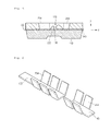
- Fig. 1 is a view of a lighting device according to a first embodiment.
- Fig. 2 is a sectional view of the lighting device along an X-axis of Fig. 1 .
- Fig. 3 is an enlarged view illustrating portions of a lead frame and a board illustrated in Fig. 2 .
- a lighting device 100 may be classified into a lateral type lighting device and a vertical type lighting device.
- the lighting device 100 may have various shapes such as a rectangular parallelepiped shape and a cube shape.
- the lighting device 100 can be used as light unit for backlight of liquid crystal display device and lighting system, etc.
- the lateral type lighting device will be described as an example.
- the lighting device 100 comprises a board 110 having a recess 120, lead frames 133 and 143, and a light emitting device 150.
- the board 110 may be formed of one of poly phthal amide (PPA), poly amide 9T (PA9T), liquid crystal polymer (LCP), and syndiotactic polystyrene (SPS). Also, the board 110 may be a printed circuit board (PCB).
- PPA poly phthal amide
- PA9T poly amide 9T
- LCP liquid crystal polymer
- SPS syndiotactic polystyrene
- PCB printed circuit board
- the board 110 has the recess 120 having a predetermined depth on a top surface thereof.
- the recess 120 may not be defined.
- a first direction of the board 110 is referred to as an X-axis direction
- a second direction of the board 110 is referred to as a Y-axis direction
- a length of the board 110 in the x-axis direction may be greater than a width of the board 110 in the Y-axis direction.
- the present disclosure is not limited to the shape of the board 110.
- the lead frames 133 and 143 may be formed on a top surface of the board 110 through injection molding.
- the lead frames 133 and 143 may be disposed within the board 110. Portions of the lead frames 133 and 143 may be exposed from the recess 120.
- the lead frames 133 and 143 may comprise lead frame protrusions 134 and 144 protruding toward the inside (Z-axis downward direction) of the board 110, respectively. That is, the lead frame protrusions 134 and 144 for increasing heat dissipation areas of the lead frames 133 and 143 formed of a metal material are disposed to improve dissipation of heat generated from the light emitting device 150.
- each of the lead frame protrusions 134 and 144 may be disposed in consideration of a distance spaced from the board 110. That is, the first lead frame protrusion 134 of the lead frame protrusions 134 and 144 may be disposed to maintain a predetermined distance or more from a side part 111 and/or a bottom part 112 of the board 110.
- the first lead frame protrusion 134 may be spaced from the side part 111 and the bottom part 112 of the board 110 by a distance of about 50 ⁇ m to about 100 ⁇ m. When the distance is less than about 50 ⁇ m, moisture may be permeated into the lead frames 133 and 143 from the outside (specifically, from a downward direction).
- each of the reference symbols A and B being greater than about 50 ⁇ m may be useful.
- the lead frames 133 and 143 and the lead frame protrusions 134 and 144 may be formed of the same metal material as each other.
- the lead frames 133 and 143 and the lead frame protrusions 134 and 144 may be formed of one of metals such as Fe, Sn, Cr, Zn, Ni, Al, Ag, Au, Cu, and combinations thereof.
- Left/right side surfaces 131 in the X-axis direction and top/bottom surfaces 132 of the recess 120 may constitute a portion of the board 110. Also, each of the left/right side surfaces 131 and top/bottom surfaces 132 of the recess 120 may be inclined at a predetermined angle. In this case, the inclined shape may be illustrated as shown in Fig. 1 .
- the light emitting device 150 may be provided on the lead frames 133 and 143 disposed in the recess 120 and connected to the lead frames 133 and 143 using wires 152. Also, the light emitting device 150 may be provided on the plurality of lead frames 133 and 143 through wire bonding, flip bonding, or die bonding. The light emitting device 150 may be disposed on the board 110 and electrically connected to the lead frames 133 and 143.
- the light emitting device 150 may comprise at least one or more LED chips of AlGaN-based, GaN-based, InGaAIP-based, GaAs-based LED chips formed of a group III-V element compound semiconductor. Also, a protection device such as a Zener diode may be provided to protect the light emitting device 150.
- the lighting device 100 may be realized by a blue LED chip and a white light emitting device using a yellow phosphor (e.g., a silicate-based phosphor), an orange phosphor, a green phosphor, and a red phosphor according to its realization configuration. Also, the lighting device 100 may be realized as a light source by at least one or more combinations of a red LED chip, a green LED chip, a blue LED chip, a yellow LED chip, a yellow green LED chip, and an UV LED chip.
- a yellow phosphor e.g., a silicate-based phosphor
- a resin material may be molded in the recess 120 to protect the light emitting device 150.
- the resin material may be formed using transparent epoxy or silicone.
- a resin material containing phosphor powder may be molded in the recess 120. Molding solution or additives may be selectively used as the resin material according to purposes for use, use environment, and characteristics of products.
- a surface of the resin material may have one shape of a flat shape, a concave lens shape, and a convex lens shape.
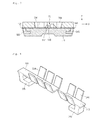
- Fig. 4 is a view of a light emitting device according to a second embodiment.
- Fig. 5 is a sectional view of the lighting device along the X-axis of Fig. 4 .
- Fig. 6 is a perspective view of a lead frame illustrated in Figs. 4 and 5 . The descriptions of the same components as those of the first embodiment will be omitted.
- a lighting device 100 comprises a board 110 having a recess 120, lead frames 133 and 143, and a light emitting device 150.
- the board 110 may be formed of one of poly phthal amide (PPA), poly amide 9T (PA9T), liquid crystal polymer (LCP), and syndiotactic polystyrene (SPS). Also, the board 110 may be a PCB.
- the lead frames 133 and 143 comprise lead frame protrusions 234 and 244 protruding toward the recess 120 (Z-axis upward direction), respectively. That is, the lead frame protrusions 234 and 244 for increasing heat dissipation areas of the lead frames 133 and 143 formed of a metal material are disposed to improve dissipation of heat generated from the light emitting device 150. As shown in Fig. 4 , the lead frame protrusions 234 and 244 are arranged around the recess 120 of the board 110. The lead frames 133 and 143 may be disposed within the board 110.
- the lead frame protrusions 234 and 244 may comprise a plurality of protrusions. Also, the lead frame protrusions 234 and 244 may be inclined at a predetermined angle, but vertically protrude from the lead frames 133 and 143 so that the lead frame protrusions 234 and 244 may be disposed along an inclined surface of the recess 120 of the board 110.
- first lead frame protrusion 234 protruding upward from the first lead frame 133 and the second lead frame protrusion 244 protruding upward from the second lead frame 143 may be provided. That is, for example, six first lead frame protrusions 234 and four second lead frame protrusions 244 are illustrated in Fig. 6 .
- a protrusion having a trunk shape as that of the first embodiment may protrude upward from the lead frame, and also, the number of protrusions may be variously changed. Also, as described in the first embodiment, a protrusion having a trunk shape may be further disposed under the lead frame.
- the lead frame protrusions 234 and 244 may be disposed outside a region of the recess 120 of the board 110. According to a modified embodiment, the lead frame protrusions 234 and 244 may be disposed along an inclined surface within the recess 120.
- the lead frames 133 and 143 and the lead frame protrusions 234 and 244 may be formed of the same metal material as each other. As described above, the lead frames 133 and 143 and the lead frame protrusions 234 and 244 may be formed of one of metals such as Fe, Sn, Cr, Zn, Ni, Al, Ag, Au, Cu, and combinations thereof. Also, the lead frames 133 and 143 and the lead frame protrusions 234 and 244 may be formed together with the recess 120 when the board 110 is formed.
- Fig. 7 is a sectional view of a light emitting device according to a third embodiment
- Fig. 8 is a perspective view of a lead frame of Fig. 7 .
- the descriptions of the same components as those of the first and second embodiments will be omitted.
- lead frames 133 and 143 may comprise protrusions, respectively.
- the lead frame protrusions extending and protruding from the lead frames 133 and 143 comprise protrusions protruding upward and protrusions protruding downward.
- the protrusions extending from the lead frames 133 and 143 may comprise first lead frame protrusions 334 and 344 protruding from the lead frames 133 and 143 in a direction (a Z-axis upward direction) of a recess 120 of a board 110 and second lead frame protrusions 335 and 345 protruding from the lead frames 133 and 143 in an inner direction (a Z-axis downward direction) of the board 110.
- the first lead frame protrusions 334 and 344 protrude upward with respect to the board 110
- the first lead frame protrusions may be referred to as lead frame upper protrusions.
- the second lead frame protrusions 335 and 345 protrude downward with respect to the board 110
- the second lead frame protrusions 335 and 345 may be referred to as lead frame lower protrusions.
- the first lead frame protrusions will be referred to as the lead frame upper protrusions
- the second lead frame protrusions will be referred to as the lead frame lower protrusions.
- the lead frame upper protrusions 334 and 344 may comprise a plurality of protrusions.
- the plurality of protrusions may be arranged around the outside of the recess 120, which is inclined at a predetermined angle.
- Each of the lead frame lower protrusions 335 and 345 has an L-shape. Also, a portion of each of the lead frame lower protrusions 335 and 345 may be disposed within the board 110. To increase heat dissipation area, each of the lead frame lower protrusions 335 and 345 may have a trunk shape, like the first embodiment.
- the lead frames 133 and 143 and the lead frame protrusions 334, 344, 335, and 345 may be integrally formed using the same metal material. As described above, the lead frames 133 and 143 and the lead frame protrusions 334, 344, 335, and 345 may be formed of one of metals such as Fe, Sn, Cr, Zn, Ni, Al, Ag, Au, Cu, and combinations thereof.
- the lighting device may be variously applicable to a display device, a light unit, and a lighting system.
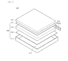
- Fig. 9 is an exploded perspective view of a display device according to an embodiment.
- a display device 1000 may comprise a light guide plate 1041, a light emitting module 1031 providing light to the light guide plate 1041, a reflective member 1022 under the light guide plate 1041, an optical sheet 1051 on the light guide plate 1041, a display panel 1061 on the optical sheet 1051, and a bottom cover 1011 receiving the light guide plate 1031, the light emitting module 1031, and the reflective member 1022, but is not limited thereto.
- the bottom cover 1011, the reflective member 1022, the light emitting module 1031, the light guide plate 1041, and the optical sheet 1051 may be defined as the light unit 1050.
- the light guide plate 1041 diffuses light to produce planar light.
- the light guide plate 1041 may be formed of a transparent material.
- the light guide plate 1041 may be formed of one of an acrylic resin-based material such as polymethylmethacrylate (PMMA), a polyethylene terephthalate (PET) resin, a poly carbonate (PC) resin, a cyclic olefin copolymer (COC) resin, and a polyethylene naphthalate (PEN) resin.
- PMMA polymethylmethacrylate
- PET polyethylene terephthalate
- PC poly carbonate
- COC cyclic olefin copolymer
- PEN polyethylene naphthalate
- the light emitting module 1031 provides light to at least one side surface of the light guide plate 1041.
- the light emitting module 1031 may be used as a light source of the display device.
- At least one light emitting module 1031 may be disposed on one side surface of the light guide plate 1041 to directly or indirectly provide light.
- the light emitting module 1031 may comprise a board 1033 and the lighting devices 100 according to the foregoing embodiments.
- the lighting devices 100 may be arrayed with a predetermined distance on the board 1033. That is, the lighting devices 100 may be arrayed on the board 1033 in a chip or package form.
- the board 1033 may be a printed circuit board (PCB) comprising a circuit pattern.
- the board 1033 may comprise at least one of a general PCB, a metal core PCB, and a flexible PCB, but is not limited thereto.
- the lighting devices 100 may be provided on a side surface of the bottom cover 1011 or on a heatsink plate, the board 1033 may be removed. Here, a portion of the heatsink plate may contact a top surface of the bottom cover 1011.
- the plurality of lighting devices 100 may be provided on the board 1033 so that a light emitting surface through which light is emitted is spaced a predetermined distance from the light guide plate 1041, but is not limited thereto.
- a light emitting device package 200 may directly or indirectly provide light to a light incident surface that is one side surface of the light guide plate 1041, but is not limited thereto.
- the reflective member 1022 may be disposed under the light guide plate 1041. Since the reflective member 1022 reflects light incident onto an under surface of the light guide plate 1041 to upwardly supply the reflected light, brightness of the light unit 1050 can be improved.
- the reflective member 1022 may be formed of one of PET, PC, and PVC, but is not limited thereto.
- the reflective member 1022 may be the top surface of the bottom cover 101 1, but is not limited thereto.
- the bottom cover 1011 may receive the light guide plate 1041, the light emitting module 1031, and the reflective member 1022.
- the bottom cover 101 may comprise a receiving part 1012 having a box shape with an opened upper side, but is not limited thereto.
- the bottom cover 101 may be coupled to a top cover, but is not limited thereto.
- the bottom cover 1011 may be formed of a metal material or a resin material. Also, the bottom cover 1011 may be manufactured using a press molding process or an extrusion molding process. The bottom cover 1011 may be formed of a metal or non-metal material having superior heat conductivity, but is not limited thereto.
- the display panel 1061 may be a liquid crystal display (LCD) panel and comprise first and second boards formed of a transparent material and a liquid crystal layer between the first and second boards.
- a polarizing plate may be attached to at least one surface of the display panel 1061. The present disclosure is not limited to the attached structure of the polarizing plate.
- the display panel 1061 transmits or blocks light provided from the light emitting module 1031 to display information.
- the display device 1000 may be applied to various portable terminals, monitors for notebook computers, monitors for laptop computers, televisions, etc.
- the optical sheet 1051 may be disposed between the display panel 1061 and the light guide plate 1041 and comprise at least one transmission sheet.
- the optical sheet 1051 may comprise at least one of a diffusion sheet, a horizontal or vertical prism sheet, a brightness enhanced sheet, etc.
- the diffusion sheet diffuses incident light
- the horizontal or/and vertical prism sheet collects the incident light into a display region.
- the brightness enhanced sheet reuses lost light to improve the brightness.
- a protection sheet may be disposed on the display panel 1061, but is not limited thereto.
- optical members such as the light guide plate 1041 and the optical sheet 1051 may be disposed on an optical path of the light emitting module 1031, but is not limited thereto.
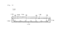
- Fig. 10 is a view illustrating another example of the display device according to an embodiment.
- a lighting device disclosed in Fig. 10 may have a structure in which light emitting devices are arrayed in a chip or package form.
- a display device 1100 comprises a bottom cover 1152, a board 1120 on which the above-described lighting devices 100 are arrayed, an optical member 1154, and a display panel 1155.
- the board 1120 and the lighting devices 100 may be defined as a light emitting module 1060.
- the bottom cover 1152, at least one light emitting module 1060, and the optical member 1154 may be defined as a light unit.
- the light emitting devices may be arrayed on the board 1129 in a chip or package form.
- the bottom cover 1152 may comprise a receiving part 1153, but is not limited thereto.
- the optical member 1154 may comprise at least one of a lens, a light guide plate, a diffusion sheet, horizontal and vertical prism sheets, and a bright enhancement sheet.
- the light guide plate may be formed of a PC material or a PMMA material. In this case, the light guide plate may be removed.
- the diffusion sheet diffuses incident light, and the horizontal and vertical prism sheets concentrate the incident light into a display region. The brightness enhanced sheet reuses lost light to improve brightness.
- Fig. 11 is a view of a lighting system according to an embodiment.
- a lighting system 1500 may comprise a case 1510, a light emitting module 1530 disposed in the case 1510, and a connection terminal 1520 disposed in the case 1510 to receive an electric power from an external power source.
- the case 1510 may be formed of a material having a good heat dissipation characteristic, for example, a metal material or a resin material.
- the light emitting module 1530 may comprise a board 1532 and a lighting device 200 provided on the board 1532.
- the lighting device 200 may be provided in plurality, and the plurality of lighting device 200 may be arrayed in a matrix shape or spaced a predetermined distance from each other. Also, light emitting devices may be arrayed on the board 1532 in a chip or package form.
- the board 1532 may be an insulator on which a circuit pattern is printed.
- the board 1532 may comprise one of a general printed circuit board (PCB), a metal core PCB, a flexible PCB, and a ceramic PCB, etc.
- PCB general printed circuit board
- metal core PCB metal core PCB
- flexible PCB flexible PCB
- ceramic PCB ceramic PCB
- the board 1532 may be formed of a material, which efficiently reflects light.
- a surface of the board 1532 may be a layer coated with a color, which efficiently reflects light, for example, a white color or a silver color.
- At least one lighting device 200 may be provided on the board 1532.
- Each of the lighting devices 200 may comprise at least one light emitting diode (LED) chip.
- the LED chip may comprise a color LED emitting red, green, blue or white light, and a UV LED emitting ultraviolet (UV) rays.
- the light emitting module 1530 may have combinations of various lighting devices 200 to obtain desired color and luminance.
- the light emitting module 1530 may have combinations of a white LED, a red LED, and a green LED to obtain a high color rendering index (CRI).
- CRI color rendering index
- connection terminal 1520 may be electrically connected to the light emitting module 1530 to supply a power.
- the connection terminal 1520 may be screw-fitted into and coupled to an external power source in a socket type, but is not limited thereto.
- the connection terminal 1520 may be made in a pin type and inserted into the external power source, or may be connected to the external power source through a wire.
- heat generated in the light emitting device may be effectively dissipated.
- any reference in this specification to "one embodiment,” “an embodiment,” “example embodiment,” etc. means that a particular feature, structure, or characteristic described in connection with the embodiment is included in at least one embodiment of the invention.
- the appearances of such phrases in various places in the specification are not necessarily all referring to the same embodiment.
Landscapes
- Planar Illumination Modules (AREA)
- Led Device Packages (AREA)
- Non-Portable Lighting Devices Or Systems Thereof (AREA)
- Arrangement Of Elements, Cooling, Sealing, Or The Like Of Lighting Devices (AREA)
- Illuminated Signs And Luminous Advertising (AREA)
Abstract
Description
- Embodiments relate to a lighting device, display device and a lighting system having the same.
- Light emitting diodes (LED) are semiconductor devices that can realize light sources having various colors using GaAs-based, AlGaAs-based, GaN-based, InGaN-based, and AlGalnP-based compound semiconductor materials.
- Characteristics of such an LED may be determined according to compound semiconductor materials used in the LED, colors, brightness, intensities of brightness, etc. Also, the LED is packaged and is being used as a light source in various fields, for example, on/off indicators displaying colors, character display devices, image display devices, etc.
- Embodiments provide a lighting device having an improved heat dissipation characteristic using a lead frame and a lighting system having the same.
- Embodiments also provide a lighting device in which at least one frame of lead frames protrudes inside a board to effectively dissipate heat generated in a light emitting device and a lighting system having the same.
- Embodiments also provide a lighting device in which at least one frame of lead frames protrudes toward a recess or a resin material to effectively dissipate heat generated in a light emitting device and a lighting system having the same.
- In one embodiment, a lighting device comprises: a board having a recess; a lead frame disposed in the recess and comprising a first lead frame protrusion protruding upward; and a light emitting device disposed on the lead frame.
- In another embodiment, a lighting device comprises: a board; a light emitting device disposed on the board; and a lead frame electrically connected to the light emitting device, wherein the lead frame comprises a first lead frame protrusion protruding upward and a second lead frame protrusion, in which a portion thereof is inserted into the board, exposed to the outside of the board to extend downward.
- In further another embodiment, a lighting system comprises: a case; a light emitting module disposed in the case and comprising at least one lighting device; and a connection terminal disposed in the case and receiving a power from an external power source, wherein the lighting device comprises a board having a recess; a lead frame disposed in the recess and comprising a first lead frame protrusion protruding upward; and a light emitting device disposed on the lead frame.
- The details of one or more embodiments are set forth in the accompanying drawings and the description below. Other features will be apparent from the description and drawings, and from the claims.
-
Fig. 1 is a view of a lighting device according to a first embodiment. -
Fig. 2 is a sectional view of the lighting device ofFig. 1 . -
Fig. 3 is an enlarged view illustrating portions of a lead frame and a board illustrated inFig. 2 . -
Fig. 4 is a view of a lighting device according to a second embodiment. -
Fig. 5 is a sectional view of the lighting device ofFig. 4 . -
Fig. 6 is a perspective view of a lead frame illustrated inFigs. 4 and5 . -
Fig. 7 is a sectional view of a lighting device according to a third embodiment. -
Fig. 8 is a perspective view of a lead frame ofFig. 7 . -
Fig. 9 is a view of a display device according to an embodiment. -
Fig. 10 is a view illustrating another example of the display device according to an embodiment. -
Fig. 11 is a view of a lighting system according to another embodiment. - In the descriptions of embodiments, it will be understood that when a layer (or film), a region, a pattern, or a structure is referred to as being 'on' a layer (or film), a region, a pad, or patterns, it can be directly on another layer, or intervening layers may also be present. Further, it will be understood that when a layer is referred to as being 'under' another layer, it can be directly under another layer, and one or more intervening layers may also be present. Further, the reference about 'on' and 'under' each layer will be made on the basis of drawings.
- In the drawings, the thickness or size of each layer is exaggerated, omitted, or schematically illustrated for convenience in description and clarity. Also, the size of each element does not entirely reflect an actual size.
- Hereinafter, exemplary embodiments will be described with reference to the accompanying drawings.
-
Fig. 1 is a view of a lighting device according to a first embodiment.Fig. 2 is a sectional view of the lighting device along an X-axis ofFig. 1 .Fig. 3 is an enlarged view illustrating portions of a lead frame and a board illustrated inFig. 2 . - A
lighting device 100 may be classified into a lateral type lighting device and a vertical type lighting device. Thelighting device 100 may have various shapes such as a rectangular parallelepiped shape and a cube shape. Thelighting device 100 can be used as light unit for backlight of liquid crystal display device and lighting system, etc. Hereinafter, for convenience of description, the lateral type lighting device will be described as an example. - The
lighting device 100 comprises aboard 110 having arecess 120,lead frames light emitting device 150. - The
board 110 may be formed of one of poly phthal amide (PPA), poly amide 9T (PA9T), liquid crystal polymer (LCP), and syndiotactic polystyrene (SPS). Also, theboard 110 may be a printed circuit board (PCB). - The
board 110 has therecess 120 having a predetermined depth on a top surface thereof. However, according to another embodiment, therecess 120 may not be defined. - Here, a first direction of the
board 110 is referred to as an X-axis direction, and a second direction of theboard 110 is referred to as a Y-axis direction. A length of theboard 110 in the x-axis direction may be greater than a width of theboard 110 in the Y-axis direction. However, the present disclosure is not limited to the shape of theboard 110. - The
lead frames board 110 through injection molding. Thelead frames board 110. Portions of thelead frames recess 120. - As shown in
Fig. 2 , thelead frames lead frame protrusions board 110, respectively. That is, thelead frame protrusions lead frames light emitting device 150. - As shown in
Fig. 3 , each of thelead frame protrusions board 110. That is, the firstlead frame protrusion 134 of thelead frame protrusions side part 111 and/or abottom part 112 of theboard 110. - For example, the first
lead frame protrusion 134 may be spaced from theside part 111 and thebottom part 112 of theboard 110 by a distance of about 50 µm to about 100 µm. When the distance is less than about 50 µm, moisture may be permeated into thelead frames - If it is assumed that a distance between the first
lead frame protrusion 134 and theside part 111 of theboard 110 is referred to as a reference symbol A and a distance between the firstlead frame protrusion 134 and thebottom part 112 of theboard 110 is referred to as a reference symbol B, each of the reference symbols A and B being greater than about 50 µm may be useful. - The
lead frames lead frame protrusions lead frames lead frame protrusions - Left/
right side surfaces 131 in the X-axis direction and top/bottom surfaces 132 of therecess 120 may constitute a portion of theboard 110. Also, each of the left/right side surfaces 131 and top/bottom surfaces 132 of therecess 120 may be inclined at a predetermined angle. In this case, the inclined shape may be illustrated as shown inFig. 1 . - The
light emitting device 150 may be provided on thelead frames recess 120 and connected to thelead frames wires 152. Also, thelight emitting device 150 may be provided on the plurality oflead frames light emitting device 150 may be disposed on theboard 110 and electrically connected to the lead frames 133 and 143. - Also, the
light emitting device 150 may comprise at least one or more LED chips of AlGaN-based, GaN-based, InGaAIP-based, GaAs-based LED chips formed of a group III-V element compound semiconductor. Also, a protection device such as a Zener diode may be provided to protect thelight emitting device 150. - The
lighting device 100 may be realized by a blue LED chip and a white light emitting device using a yellow phosphor (e.g., a silicate-based phosphor), an orange phosphor, a green phosphor, and a red phosphor according to its realization configuration. Also, thelighting device 100 may be realized as a light source by at least one or more combinations of a red LED chip, a green LED chip, a blue LED chip, a yellow LED chip, a yellow green LED chip, and an UV LED chip. - A resin material may be molded in the
recess 120 to protect thelight emitting device 150. The resin material may be formed using transparent epoxy or silicone. Alternatively, as necessary, a resin material containing phosphor powder may be molded in therecess 120. Molding solution or additives may be selectively used as the resin material according to purposes for use, use environment, and characteristics of products. Also, a surface of the resin material may have one shape of a flat shape, a concave lens shape, and a convex lens shape. -
Fig. 4 is a view of a light emitting device according to a second embodiment.Fig. 5 is a sectional view of the lighting device along the X-axis ofFig. 4 .Fig. 6 is a perspective view of a lead frame illustrated inFigs. 4 and5 . The descriptions of the same components as those of the first embodiment will be omitted. - A
lighting device 100 according to a second embodiment comprises aboard 110 having arecess 120,lead frames light emitting device 150. Theboard 110 may be formed of one of poly phthal amide (PPA), poly amide 9T (PA9T), liquid crystal polymer (LCP), and syndiotactic polystyrene (SPS). Also, theboard 110 may be a PCB. - As shown in
Fig. 5 , the lead frames 133 and 143 according to the second embodiment compriselead frame protrusions lead frame protrusions light emitting device 150. As shown inFig. 4 , thelead frame protrusions recess 120 of theboard 110. The lead frames 133 and 143 may be disposed within theboard 110. - As shown in
Fig. 6 , thelead frame protrusions lead frame protrusions lead frame protrusions recess 120 of theboard 110. - In
Fig. 6 , the firstlead frame protrusion 234 protruding upward from thefirst lead frame 133 and the secondlead frame protrusion 244 protruding upward from thesecond lead frame 143 may be provided. That is, for example, six firstlead frame protrusions 234 and four secondlead frame protrusions 244 are illustrated inFig. 6 . - However, the number and configuration of the lead frame protrusions are only an example. According to a modified embodiment, a protrusion having a trunk shape as that of the first embodiment may protrude upward from the lead frame, and also, the number of protrusions may be variously changed. Also, as described in the first embodiment, a protrusion having a trunk shape may be further disposed under the lead frame.
- As shown in
Fig. 4 , thelead frame protrusions recess 120 of theboard 110. According to a modified embodiment, thelead frame protrusions recess 120. - The lead frames 133 and 143 and the
lead frame protrusions lead frame protrusions lead frame protrusions recess 120 when theboard 110 is formed. -
Fig. 7 is a sectional view of a light emitting device according to a third embodiment, andFig. 8 is a perspective view of a lead frame ofFig. 7 . The descriptions of the same components as those of the first and second embodiments will be omitted. - As shown in
Figs. 7 and 8 , in a lighting device according to a third embodiment, lead frames 133 and 143 may comprise protrusions, respectively. The lead frame protrusions extending and protruding from the lead frames 133 and 143 comprise protrusions protruding upward and protrusions protruding downward. - That is, the protrusions extending from the lead frames 133 and 143 may comprise first
lead frame protrusions recess 120 of aboard 110 and secondlead frame protrusions board 110. Here, since the firstlead frame protrusions board 110, the first lead frame protrusions may be referred to as lead frame upper protrusions. Also, since the secondlead frame protrusions board 110, the secondlead frame protrusions - Hereinafter, for better comprehension, the first lead frame protrusions will be referred to as the lead frame upper protrusions, and the second lead frame protrusions will be referred to as the lead frame lower protrusions.
- Like the second embodiment, the lead frame
upper protrusions recess 120, which is inclined at a predetermined angle. - Each of the lead frame
lower protrusions lower protrusions board 110. To increase heat dissipation area, each of the lead framelower protrusions - In the lead frame protrusions according to the third embodiment, since heat generated in the
light emitting device 150 may be dissipated in upward and downward directions, a heat dissipation characteristic can be further improved. - The lead frames 133 and 143 and the
lead frame protrusions lead frame protrusions - The lighting device according to the foregoing embodiments may be variously applicable to a display device, a light unit, and a lighting system.
-
Fig. 9 is an exploded perspective view of a display device according to an embodiment. - Referring to
Fig. 9 , adisplay device 1000 according to an embodiment may comprise alight guide plate 1041, alight emitting module 1031 providing light to thelight guide plate 1041, areflective member 1022 under thelight guide plate 1041, anoptical sheet 1051 on thelight guide plate 1041, adisplay panel 1061 on theoptical sheet 1051, and abottom cover 1011 receiving thelight guide plate 1031, thelight emitting module 1031, and thereflective member 1022, but is not limited thereto. - The
bottom cover 1011, thereflective member 1022, thelight emitting module 1031, thelight guide plate 1041, and theoptical sheet 1051 may be defined as thelight unit 1050. - The
light guide plate 1041 diffuses light to produce planar light. Thelight guide plate 1041 may be formed of a transparent material. For example, thelight guide plate 1041 may be formed of one of an acrylic resin-based material such as polymethylmethacrylate (PMMA), a polyethylene terephthalate (PET) resin, a poly carbonate (PC) resin, a cyclic olefin copolymer (COC) resin, and a polyethylene naphthalate (PEN) resin. - The
light emitting module 1031 provides light to at least one side surface of thelight guide plate 1041. Thus, thelight emitting module 1031 may be used as a light source of the display device. - At least one light emitting
module 1031 may be disposed on one side surface of thelight guide plate 1041 to directly or indirectly provide light. Thelight emitting module 1031 may comprise a board 1033 and thelighting devices 100 according to the foregoing embodiments. Thelighting devices 100 may be arrayed with a predetermined distance on the board 1033. That is, thelighting devices 100 may be arrayed on the board 1033 in a chip or package form. - The board 1033 may be a printed circuit board (PCB) comprising a circuit pattern. Alternatively, the board 1033 may comprise at least one of a general PCB, a metal core PCB, and a flexible PCB, but is not limited thereto. The
lighting devices 100 may be provided on a side surface of thebottom cover 1011 or on a heatsink plate, the board 1033 may be removed. Here, a portion of the heatsink plate may contact a top surface of thebottom cover 1011. - The plurality of
lighting devices 100 may be provided on the board 1033 so that a light emitting surface through which light is emitted is spaced a predetermined distance from thelight guide plate 1041, but is not limited thereto. A light emittingdevice package 200 may directly or indirectly provide light to a light incident surface that is one side surface of thelight guide plate 1041, but is not limited thereto. - The
reflective member 1022 may be disposed under thelight guide plate 1041. Since thereflective member 1022 reflects light incident onto an under surface of thelight guide plate 1041 to upwardly supply the reflected light, brightness of thelight unit 1050 can be improved. For example, thereflective member 1022 may be formed of one of PET, PC, and PVC, but is not limited thereto. Thereflective member 1022 may be the top surface of the bottom cover 101 1, but is not limited thereto. - The
bottom cover 1011 may receive thelight guide plate 1041, thelight emitting module 1031, and thereflective member 1022. For this, the bottom cover 101 may comprise a receivingpart 1012 having a box shape with an opened upper side, but is not limited thereto. The bottom cover 101 may be coupled to a top cover, but is not limited thereto. - The
bottom cover 1011 may be formed of a metal material or a resin material. Also, thebottom cover 1011 may be manufactured using a press molding process or an extrusion molding process. Thebottom cover 1011 may be formed of a metal or non-metal material having superior heat conductivity, but is not limited thereto. - For example, the
display panel 1061 may be a liquid crystal display (LCD) panel and comprise first and second boards formed of a transparent material and a liquid crystal layer between the first and second boards. A polarizing plate may be attached to at least one surface of thedisplay panel 1061. The present disclosure is not limited to the attached structure of the polarizing plate. Thedisplay panel 1061 transmits or blocks light provided from thelight emitting module 1031 to display information. Thedisplay device 1000 may be applied to various portable terminals, monitors for notebook computers, monitors for laptop computers, televisions, etc. - The
optical sheet 1051 may be disposed between thedisplay panel 1061 and thelight guide plate 1041 and comprise at least one transmission sheet. For example, theoptical sheet 1051 may comprise at least one of a diffusion sheet, a horizontal or vertical prism sheet, a brightness enhanced sheet, etc. The diffusion sheet diffuses incident light, and the horizontal or/and vertical prism sheet collects the incident light into a display region. In addition, the brightness enhanced sheet reuses lost light to improve the brightness. Also, a protection sheet may be disposed on thedisplay panel 1061, but is not limited thereto. - Here, optical members such as the
light guide plate 1041 and theoptical sheet 1051 may be disposed on an optical path of thelight emitting module 1031, but is not limited thereto. -
Fig. 10 is a view illustrating another example of the display device according to an embodiment. A lighting device disclosed inFig. 10 may have a structure in which light emitting devices are arrayed in a chip or package form. - Referring to
Fig. 10 , adisplay device 1100 comprises abottom cover 1152, aboard 1120 on which the above-describedlighting devices 100 are arrayed, anoptical member 1154, and adisplay panel 1155. - The
board 1120 and thelighting devices 100 may be defined as a light emitting module 1060. Thebottom cover 1152, at least one light emitting module 1060, and theoptical member 1154 may be defined as a light unit. The light emitting devices may be arrayed on the board 1129 in a chip or package form. - The
bottom cover 1152 may comprise a receivingpart 1153, but is not limited thereto. - Here, the
optical member 1154 may comprise at least one of a lens, a light guide plate, a diffusion sheet, horizontal and vertical prism sheets, and a bright enhancement sheet. The light guide plate may be formed of a PC material or a PMMA material. In this case, the light guide plate may be removed. The diffusion sheet diffuses incident light, and the horizontal and vertical prism sheets concentrate the incident light into a display region. The brightness enhanced sheet reuses lost light to improve brightness. -
Fig. 11 is a view of a lighting system according to an embodiment. - Referring to
Fig. 11 , alighting system 1500 may comprise acase 1510, alight emitting module 1530 disposed in thecase 1510, and aconnection terminal 1520 disposed in thecase 1510 to receive an electric power from an external power source. - The
case 1510 may be formed of a material having a good heat dissipation characteristic, for example, a metal material or a resin material. - The
light emitting module 1530 may comprise aboard 1532 and alighting device 200 provided on theboard 1532. Thelighting device 200 may be provided in plurality, and the plurality oflighting device 200 may be arrayed in a matrix shape or spaced a predetermined distance from each other. Also, light emitting devices may be arrayed on theboard 1532 in a chip or package form. - The
board 1532 may be an insulator on which a circuit pattern is printed. For example, theboard 1532 may comprise one of a general printed circuit board (PCB), a metal core PCB, a flexible PCB, and a ceramic PCB, etc. - Also, the
board 1532 may be formed of a material, which efficiently reflects light. Alternatively, a surface of theboard 1532 may be a layer coated with a color, which efficiently reflects light, for example, a white color or a silver color. - At least one
lighting device 200 may be provided on theboard 1532. Each of thelighting devices 200 may comprise at least one light emitting diode (LED) chip. The LED chip may comprise a color LED emitting red, green, blue or white light, and a UV LED emitting ultraviolet (UV) rays. - The
light emitting module 1530 may have combinations ofvarious lighting devices 200 to obtain desired color and luminance. For example, thelight emitting module 1530 may have combinations of a white LED, a red LED, and a green LED to obtain a high color rendering index (CRI). - The
connection terminal 1520 may be electrically connected to thelight emitting module 1530 to supply a power. Theconnection terminal 1520 may be screw-fitted into and coupled to an external power source in a socket type, but is not limited thereto. For example, theconnection terminal 1520 may be made in a pin type and inserted into the external power source, or may be connected to the external power source through a wire. - In the lighting device and the lighting system having the same according to the embodiments, heat generated in the light emitting device may be effectively dissipated.
- Any reference in this specification to "one embodiment," "an embodiment," "example embodiment," etc., means that a particular feature, structure, or characteristic described in connection with the embodiment is included in at least one embodiment of the invention. The appearances of such phrases in various places in the specification are not necessarily all referring to the same embodiment. Further, when a particular feature, structure, or characteristic is described in connection with any embodiment, it is submitted that it is within the purview of one skilled in the art to effect such feature, structure, or characteristic in connection with other ones of the embodiments.
- Although embodiments have been described with reference to a number of illustrative embodiments thereof, it should be understood that numerous other modifications and embodiments can be devised by those skilled in the art that will fall within the spirit and scope of the principles of this disclosure. More particularly, various variations and modifications are possible in the component parts and/or arrangements of the subject combination arrangement within the scope of the disclosure, the drawings and the appended claims. In addition to variations and modifications in the component parts and/or arrangements, alternative uses will also be apparent to those skilled in the art.
Claims (15)
- A lighting device comprising:a board having a recess;a lead frame disposed in the recess and comprising a first lead frame protrusion protruding upward; anda light emitting device disposed on the lead frame.
- The lighting device of claim 1, wherein the first lead frame protrusion is disposed along a circumference of an inner inclined surface of the recess.
- The lighting device of claim 1, wherein the first lead frame protrusion comprises a plurality of protrusions.
- The lighting device of claim 1, wherein the lead frame comprises a second lead frame protrusion protruding downward in the board.
- The lighting device of claim 4, wherein the second lead frame protrusion has a thickness greater than that of the other portion of the lead frame.
- The lighting device of claim 4, wherein the second lead frame protrusion has side and bottom surfaces surrounded by the board.
- The lighting device of claim 4, wherein the second lead frame protrusion is spaced about 5 µm or more from bottom or side surfaces of the board.
- The lighting device of claim 4, wherein the lead frame and the second lead frame protrusion are formed of the same material.
- The lighting device of claim 1, further comprising a third lead frame protrusion in which a portion thereof is inserted into the board, the third lead frame protrusion extending downward from the lead frame.
- The lighting device of claim 9, wherein the lead frame and the third lead frame protrusion are formed of the same material.
- The lighting device of claim 1, wherein the lead frame is disposed within the board.
- A display device comprising:a light emitting module comprising at least one lighting device of any one of claims 1 to 11;a light guide plate disposed on one side of the light emitting module; anda display panel disposed on the light guide plate.
- The display device of claim 12, further comprising an optical sheet disposed on the light guide plate.
- The display device of claim 12, further comprising a reflective member disposed under the light guide plate.
- A lighting system comprising:a case;a light emitting module disposed in the case and comprising at least one lighting device of any one of claims 1 to 11; anda connection terminal disposed in the case to receive a power from an external power source.
Applications Claiming Priority (1)
| Application Number | Priority Date | Filing Date | Title |
|---|---|---|---|
| KR1020100029941A KR101047676B1 (en) | 2010-04-01 | 2010-04-01 | Light emitting device and light unit having same |
Publications (3)
| Publication Number | Publication Date |
|---|---|
| EP2372794A2 true EP2372794A2 (en) | 2011-10-05 |
| EP2372794A3 EP2372794A3 (en) | 2015-12-23 |
| EP2372794B1 EP2372794B1 (en) | 2019-11-20 |
Family
ID=44168416
Family Applications (1)
| Application Number | Title | Priority Date | Filing Date |
|---|---|---|---|
| EP11160354.4A Active EP2372794B1 (en) | 2010-04-01 | 2011-03-30 | Lighting device, display device and lighting system having the same |
Country Status (4)
| Country | Link |
|---|---|
| US (1) | US9076942B2 (en) |
| EP (1) | EP2372794B1 (en) |
| KR (1) | KR101047676B1 (en) |
| CN (1) | CN102213373B (en) |
Families Citing this family (1)
| Publication number | Priority date | Publication date | Assignee | Title |
|---|---|---|---|---|
| KR20120093679A (en) * | 2011-02-15 | 2012-08-23 | 삼성전자주식회사 | Light emitting device package and manufacturing method thereof |
Family Cites Families (18)
| Publication number | Priority date | Publication date | Assignee | Title |
|---|---|---|---|---|
| JP2003152228A (en) * | 2001-11-12 | 2003-05-23 | Sumitomo Bakelite Co Ltd | LED case and LED light emitter |
| JP2004146815A (en) * | 2002-09-30 | 2004-05-20 | Sanyo Electric Co Ltd | Light emitting element |
| JP3910171B2 (en) | 2003-02-18 | 2007-04-25 | シャープ株式会社 | Semiconductor light emitting device, method for manufacturing the same, and electronic imaging device |
| JP2005116937A (en) | 2003-10-10 | 2005-04-28 | Matsushita Electric Ind Co Ltd | Semiconductor light emitting device and manufacturing method thereof |
| JP2007012727A (en) * | 2005-06-29 | 2007-01-18 | Toyoda Gosei Co Ltd | Light emitting device |
| JP2007142044A (en) | 2005-11-16 | 2007-06-07 | Stanley Electric Co Ltd | Semiconductor light emitting device and surface light source using the same |
| JP2007184534A (en) | 2005-12-09 | 2007-07-19 | Matsushita Electric Ind Co Ltd | LIGHT EMITTING MODULE, ITS MANUFACTURING METHOD, AND BACKLIGHT DEVICE USING THE SAME |
| KR101224376B1 (en) | 2006-01-25 | 2013-01-21 | 삼성디스플레이 주식회사 | Backlight assembly and liquid crystal display apparatus having the same |
| JP2007329152A (en) * | 2006-06-06 | 2007-12-20 | Matsushita Electric Ind Co Ltd | Glass, glass manufacturing method, semiconductor light emitting device, and semiconductor light emitting device manufacturing method |
| JP2008016744A (en) * | 2006-07-10 | 2008-01-24 | Matsushita Electric Ind Co Ltd | Package for semiconductor light emitting device and method for manufacturing the same |
| KR100772433B1 (en) * | 2006-08-23 | 2007-11-01 | 서울반도체 주식회사 | LED package adopting lead terminal with reflecting surface |
| JP5060172B2 (en) | 2007-05-29 | 2012-10-31 | 岩谷産業株式会社 | Semiconductor light emitting device |
| KR20090003740U (en) * | 2007-10-17 | 2009-04-22 | 엘지이노텍 주식회사 | LED Package |
| JP5186930B2 (en) * | 2008-01-24 | 2013-04-24 | 豊田合成株式会社 | Light emitting device |
| KR100986202B1 (en) * | 2008-07-01 | 2010-10-07 | 알티전자 주식회사 | Side view light emitting diode package |
| JP2010021259A (en) * | 2008-07-09 | 2010-01-28 | Toshiba Corp | Optical semiconductor device |
| US8288785B2 (en) * | 2008-12-03 | 2012-10-16 | Seoul Semiconductor Co., Ltd. | Lead frame having light-reflecting layer, light emitting diode having the lead frame, and backlight unit having the light emitting diode |
| CN201344485Y (en) | 2008-12-12 | 2009-11-11 | 张宇 | LED polyhedral lamp |
-
2010
- 2010-04-01 KR KR1020100029941A patent/KR101047676B1/en not_active Expired - Fee Related
-
2011
- 2011-03-30 EP EP11160354.4A patent/EP2372794B1/en active Active
- 2011-03-30 US US13/075,405 patent/US9076942B2/en active Active
- 2011-04-01 CN CN201110086632.0A patent/CN102213373B/en not_active Expired - Fee Related
Non-Patent Citations (1)
| Title |
|---|
| None |
Also Published As
| Publication number | Publication date |
|---|---|
| US20110242825A1 (en) | 2011-10-06 |
| CN102213373A (en) | 2011-10-12 |
| KR101047676B1 (en) | 2011-07-08 |
| EP2372794B1 (en) | 2019-11-20 |
| EP2372794A3 (en) | 2015-12-23 |
| CN102213373B (en) | 2015-07-01 |
| US9076942B2 (en) | 2015-07-07 |
Similar Documents
| Publication | Publication Date | Title |
|---|---|---|
| EP2346100B1 (en) | Light emitting apparatus and lighting system | |
| US8598616B2 (en) | Light emitting device and light unit using the same | |
| CN102097423B (en) | Light emitting device package and illuminator | |
| JP5204866B2 (en) | Light emitting device package and lighting system including the same | |
| CN102157504B (en) | Light emitting diode package and light unit having the same | |
| US8783933B2 (en) | Light emitting device package, and display apparatus and lighting system having the same | |
| KR20110128693A (en) | Light emitting device package and light unit having same | |
| KR20110105056A (en) | Light emitting device, light emitting device manufacturing method, light unit and lighting device | |
| KR101766720B1 (en) | Light Emitting Device Package | |
| US9076942B2 (en) | Lighting device and lighting system having the same | |
| KR101978942B1 (en) | Light Emitting Device Package | |
| KR101944794B1 (en) | Light emitting device package and lighting systme having thereof | |
| KR101683887B1 (en) | Light emitting device package and light unit having thereof | |
| KR20110107637A (en) | Printed circuit board and manufacturing method thereof, light emitting device package, light emitting device and lighting system | |
| KR101878863B1 (en) | The light emitting device package and the light emitting system | |
| KR20130061421A (en) | Light emitting package | |
| KR20120037263A (en) | Light emitting device package | |
| KR20120035464A (en) | Light emitting device package | |
| KR20120014419A (en) | The light- | |
| KR20120044111A (en) | Light emitting device package and light unit | |
| KR20120060990A (en) | Light Emitting Device Module | |
| KR20120103039A (en) | Light emitting device module |
Legal Events
| Date | Code | Title | Description |
|---|---|---|---|
| PUAI | Public reference made under article 153(3) epc to a published international application that has entered the european phase |
Free format text: ORIGINAL CODE: 0009012 |
|
| AK | Designated contracting states |
Kind code of ref document: A2 Designated state(s): AL AT BE BG CH CY CZ DE DK EE ES FI FR GB GR HR HU IE IS IT LI LT LU LV MC MK MT NL NO PL PT RO RS SE SI SK SM TR |
|
| AX | Request for extension of the european patent |
Extension state: BA ME |
|
| 17P | Request for examination filed |
Effective date: 20140328 |
|
| RBV | Designated contracting states (corrected) |
Designated state(s): AL AT BE BG CH CY CZ DE DK EE ES FI FR GB GR HR HU IE IS IT LI LT LU LV MC MK MT NL NO PL PT RO RS SE SI SK SM TR |
|
| RAP1 | Party data changed (applicant data changed or rights of an application transferred) |
Owner name: LG INNOTEK CO., LTD. |
|
| PUAL | Search report despatched |
Free format text: ORIGINAL CODE: 0009013 |
|
| AK | Designated contracting states |
Kind code of ref document: A3 Designated state(s): AL AT BE BG CH CY CZ DE DK EE ES FI FR GB GR HR HU IE IS IT LI LT LU LV MC MK MT NL NO PL PT RO RS SE SI SK SM TR |
|
| AX | Request for extension of the european patent |
Extension state: BA ME |
|
| RIC1 | Information provided on ipc code assigned before grant |
Ipc: H01L 33/62 20100101AFI20151116BHEP Ipc: H01L 33/64 20100101ALI20151116BHEP |
|
| RAP1 | Party data changed (applicant data changed or rights of an application transferred) |
Owner name: LG INNOTEK CO., LTD. |
|
| STAA | Information on the status of an ep patent application or granted ep patent |
Free format text: STATUS: EXAMINATION IS IN PROGRESS |
|
| 17Q | First examination report despatched |
Effective date: 20190205 |
|
| GRAP | Despatch of communication of intention to grant a patent |
Free format text: ORIGINAL CODE: EPIDOSNIGR1 |
|
| STAA | Information on the status of an ep patent application or granted ep patent |
Free format text: STATUS: GRANT OF PATENT IS INTENDED |
|
| INTG | Intention to grant announced |
Effective date: 20190607 |
|
| GRAS | Grant fee paid |
Free format text: ORIGINAL CODE: EPIDOSNIGR3 |
|
| GRAA | (expected) grant |
Free format text: ORIGINAL CODE: 0009210 |
|
| STAA | Information on the status of an ep patent application or granted ep patent |
Free format text: STATUS: THE PATENT HAS BEEN GRANTED |
|
| AK | Designated contracting states |
Kind code of ref document: B1 Designated state(s): AL AT BE BG CH CY CZ DE DK EE ES FI FR GB GR HR HU IE IS IT LI LT LU LV MC MK MT NL NO PL PT RO RS SE SI SK SM TR |
|
| REG | Reference to a national code |
Ref country code: GB Ref legal event code: FG4D |
|
| REG | Reference to a national code |
Ref country code: CH Ref legal event code: EP |
|
| REG | Reference to a national code |
Ref country code: IE Ref legal event code: FG4D |
|
| REG | Reference to a national code |
Ref country code: DE Ref legal event code: R096 Ref document number: 602011063449 Country of ref document: DE |
|
| REG | Reference to a national code |
Ref country code: AT Ref legal event code: REF Ref document number: 1205182 Country of ref document: AT Kind code of ref document: T Effective date: 20191215 |
|
| REG | Reference to a national code |
Ref country code: NL Ref legal event code: MP Effective date: 20191120 |
|
| REG | Reference to a national code |
Ref country code: LT Ref legal event code: MG4D |
|
| PG25 | Lapsed in a contracting state [announced via postgrant information from national office to epo] |
Ref country code: GR Free format text: LAPSE BECAUSE OF FAILURE TO SUBMIT A TRANSLATION OF THE DESCRIPTION OR TO PAY THE FEE WITHIN THE PRESCRIBED TIME-LIMIT Effective date: 20200221 Ref country code: NO Free format text: LAPSE BECAUSE OF FAILURE TO SUBMIT A TRANSLATION OF THE DESCRIPTION OR TO PAY THE FEE WITHIN THE PRESCRIBED TIME-LIMIT Effective date: 20200220 Ref country code: FI Free format text: LAPSE BECAUSE OF FAILURE TO SUBMIT A TRANSLATION OF THE DESCRIPTION OR TO PAY THE FEE WITHIN THE PRESCRIBED TIME-LIMIT Effective date: 20191120 Ref country code: BG Free format text: LAPSE BECAUSE OF FAILURE TO SUBMIT A TRANSLATION OF THE DESCRIPTION OR TO PAY THE FEE WITHIN THE PRESCRIBED TIME-LIMIT Effective date: 20200220 Ref country code: LT Free format text: LAPSE BECAUSE OF FAILURE TO SUBMIT A TRANSLATION OF THE DESCRIPTION OR TO PAY THE FEE WITHIN THE PRESCRIBED TIME-LIMIT Effective date: 20191120 Ref country code: LV Free format text: LAPSE BECAUSE OF FAILURE TO SUBMIT A TRANSLATION OF THE DESCRIPTION OR TO PAY THE FEE WITHIN THE PRESCRIBED TIME-LIMIT Effective date: 20191120 Ref country code: SE Free format text: LAPSE BECAUSE OF FAILURE TO SUBMIT A TRANSLATION OF THE DESCRIPTION OR TO PAY THE FEE WITHIN THE PRESCRIBED TIME-LIMIT Effective date: 20191120 Ref country code: ES Free format text: LAPSE BECAUSE OF FAILURE TO SUBMIT A TRANSLATION OF THE DESCRIPTION OR TO PAY THE FEE WITHIN THE PRESCRIBED TIME-LIMIT Effective date: 20191120 Ref country code: NL Free format text: LAPSE BECAUSE OF FAILURE TO SUBMIT A TRANSLATION OF THE DESCRIPTION OR TO PAY THE FEE WITHIN THE PRESCRIBED TIME-LIMIT Effective date: 20191120 |
|
| PG25 | Lapsed in a contracting state [announced via postgrant information from national office to epo] |
Ref country code: IS Free format text: LAPSE BECAUSE OF FAILURE TO SUBMIT A TRANSLATION OF THE DESCRIPTION OR TO PAY THE FEE WITHIN THE PRESCRIBED TIME-LIMIT Effective date: 20200320 Ref country code: HR Free format text: LAPSE BECAUSE OF FAILURE TO SUBMIT A TRANSLATION OF THE DESCRIPTION OR TO PAY THE FEE WITHIN THE PRESCRIBED TIME-LIMIT Effective date: 20191120 Ref country code: RS Free format text: LAPSE BECAUSE OF FAILURE TO SUBMIT A TRANSLATION OF THE DESCRIPTION OR TO PAY THE FEE WITHIN THE PRESCRIBED TIME-LIMIT Effective date: 20191120 |
|
| PG25 | Lapsed in a contracting state [announced via postgrant information from national office to epo] |
Ref country code: AL Free format text: LAPSE BECAUSE OF FAILURE TO SUBMIT A TRANSLATION OF THE DESCRIPTION OR TO PAY THE FEE WITHIN THE PRESCRIBED TIME-LIMIT Effective date: 20191120 |
|
| PG25 | Lapsed in a contracting state [announced via postgrant information from national office to epo] |
Ref country code: DK Free format text: LAPSE BECAUSE OF FAILURE TO SUBMIT A TRANSLATION OF THE DESCRIPTION OR TO PAY THE FEE WITHIN THE PRESCRIBED TIME-LIMIT Effective date: 20191120 Ref country code: PT Free format text: LAPSE BECAUSE OF FAILURE TO SUBMIT A TRANSLATION OF THE DESCRIPTION OR TO PAY THE FEE WITHIN THE PRESCRIBED TIME-LIMIT Effective date: 20200412 Ref country code: EE Free format text: LAPSE BECAUSE OF FAILURE TO SUBMIT A TRANSLATION OF THE DESCRIPTION OR TO PAY THE FEE WITHIN THE PRESCRIBED TIME-LIMIT Effective date: 20191120 Ref country code: RO Free format text: LAPSE BECAUSE OF FAILURE TO SUBMIT A TRANSLATION OF THE DESCRIPTION OR TO PAY THE FEE WITHIN THE PRESCRIBED TIME-LIMIT Effective date: 20191120 Ref country code: CZ Free format text: LAPSE BECAUSE OF FAILURE TO SUBMIT A TRANSLATION OF THE DESCRIPTION OR TO PAY THE FEE WITHIN THE PRESCRIBED TIME-LIMIT Effective date: 20191120 |
|
| REG | Reference to a national code |
Ref country code: AT Ref legal event code: MK05 Ref document number: 1205182 Country of ref document: AT Kind code of ref document: T Effective date: 20191120 |
|
| REG | Reference to a national code |
Ref country code: DE Ref legal event code: R097 Ref document number: 602011063449 Country of ref document: DE |
|
| PG25 | Lapsed in a contracting state [announced via postgrant information from national office to epo] |
Ref country code: SM Free format text: LAPSE BECAUSE OF FAILURE TO SUBMIT A TRANSLATION OF THE DESCRIPTION OR TO PAY THE FEE WITHIN THE PRESCRIBED TIME-LIMIT Effective date: 20191120 Ref country code: SK Free format text: LAPSE BECAUSE OF FAILURE TO SUBMIT A TRANSLATION OF THE DESCRIPTION OR TO PAY THE FEE WITHIN THE PRESCRIBED TIME-LIMIT Effective date: 20191120 |
|
| PLBE | No opposition filed within time limit |
Free format text: ORIGINAL CODE: 0009261 |
|
| STAA | Information on the status of an ep patent application or granted ep patent |
Free format text: STATUS: NO OPPOSITION FILED WITHIN TIME LIMIT |
|
| 26N | No opposition filed |
Effective date: 20200821 |
|
| PG25 | Lapsed in a contracting state [announced via postgrant information from national office to epo] |
Ref country code: MC Free format text: LAPSE BECAUSE OF FAILURE TO SUBMIT A TRANSLATION OF THE DESCRIPTION OR TO PAY THE FEE WITHIN THE PRESCRIBED TIME-LIMIT Effective date: 20191120 |
|
| REG | Reference to a national code |
Ref country code: CH Ref legal event code: PL |
|
| PG25 | Lapsed in a contracting state [announced via postgrant information from national office to epo] |
Ref country code: PL Free format text: LAPSE BECAUSE OF FAILURE TO SUBMIT A TRANSLATION OF THE DESCRIPTION OR TO PAY THE FEE WITHIN THE PRESCRIBED TIME-LIMIT Effective date: 20191120 Ref country code: AT Free format text: LAPSE BECAUSE OF FAILURE TO SUBMIT A TRANSLATION OF THE DESCRIPTION OR TO PAY THE FEE WITHIN THE PRESCRIBED TIME-LIMIT Effective date: 20191120 Ref country code: SI Free format text: LAPSE BECAUSE OF FAILURE TO SUBMIT A TRANSLATION OF THE DESCRIPTION OR TO PAY THE FEE WITHIN THE PRESCRIBED TIME-LIMIT Effective date: 20191120 |
|
| REG | Reference to a national code |
Ref country code: BE Ref legal event code: MM Effective date: 20200331 |
|
| PG25 | Lapsed in a contracting state [announced via postgrant information from national office to epo] |
Ref country code: LU Free format text: LAPSE BECAUSE OF NON-PAYMENT OF DUE FEES Effective date: 20200330 |
|
| PG25 | Lapsed in a contracting state [announced via postgrant information from national office to epo] |
Ref country code: CH Free format text: LAPSE BECAUSE OF NON-PAYMENT OF DUE FEES Effective date: 20200331 Ref country code: LI Free format text: LAPSE BECAUSE OF NON-PAYMENT OF DUE FEES Effective date: 20200331 Ref country code: IT Free format text: LAPSE BECAUSE OF FAILURE TO SUBMIT A TRANSLATION OF THE DESCRIPTION OR TO PAY THE FEE WITHIN THE PRESCRIBED TIME-LIMIT Effective date: 20191120 Ref country code: IE Free format text: LAPSE BECAUSE OF NON-PAYMENT OF DUE FEES Effective date: 20200330 Ref country code: FR Free format text: LAPSE BECAUSE OF NON-PAYMENT OF DUE FEES Effective date: 20200331 |
|
| PG25 | Lapsed in a contracting state [announced via postgrant information from national office to epo] |
Ref country code: BE Free format text: LAPSE BECAUSE OF NON-PAYMENT OF DUE FEES Effective date: 20200331 |
|
| GBPC | Gb: european patent ceased through non-payment of renewal fee |
Effective date: 20200330 |
|
| PG25 | Lapsed in a contracting state [announced via postgrant information from national office to epo] |
Ref country code: GB Free format text: LAPSE BECAUSE OF NON-PAYMENT OF DUE FEES Effective date: 20200330 |
|
| REG | Reference to a national code |
Ref country code: DE Ref legal event code: R081 Ref document number: 602011063449 Country of ref document: DE Owner name: SUZHOU LEKIN SEMICONDUCTOR CO. LTD., TAICANG, CN Free format text: FORMER OWNER: LG INNOTEK CO., LTD., SEOUL, KR |
|
| PG25 | Lapsed in a contracting state [announced via postgrant information from national office to epo] |
Ref country code: TR Free format text: LAPSE BECAUSE OF FAILURE TO SUBMIT A TRANSLATION OF THE DESCRIPTION OR TO PAY THE FEE WITHIN THE PRESCRIBED TIME-LIMIT Effective date: 20191120 Ref country code: MT Free format text: LAPSE BECAUSE OF FAILURE TO SUBMIT A TRANSLATION OF THE DESCRIPTION OR TO PAY THE FEE WITHIN THE PRESCRIBED TIME-LIMIT Effective date: 20191120 Ref country code: CY Free format text: LAPSE BECAUSE OF FAILURE TO SUBMIT A TRANSLATION OF THE DESCRIPTION OR TO PAY THE FEE WITHIN THE PRESCRIBED TIME-LIMIT Effective date: 20191120 |
|
| PG25 | Lapsed in a contracting state [announced via postgrant information from national office to epo] |
Ref country code: MK Free format text: LAPSE BECAUSE OF FAILURE TO SUBMIT A TRANSLATION OF THE DESCRIPTION OR TO PAY THE FEE WITHIN THE PRESCRIBED TIME-LIMIT Effective date: 20191120 |
|
| PGFP | Annual fee paid to national office [announced via postgrant information from national office to epo] |
Ref country code: DE Payment date: 20230214 Year of fee payment: 13 |
|
| REG | Reference to a national code |
Ref country code: DE Ref legal event code: R119 Ref document number: 602011063449 Country of ref document: DE |
|
| PG25 | Lapsed in a contracting state [announced via postgrant information from national office to epo] |
Ref country code: DE Free format text: LAPSE BECAUSE OF NON-PAYMENT OF DUE FEES Effective date: 20241001 |
|
| PG25 | Lapsed in a contracting state [announced via postgrant information from national office to epo] |
Ref country code: DE Free format text: LAPSE BECAUSE OF NON-PAYMENT OF DUE FEES Effective date: 20241001 |