EP2360745A2 - Lichtemittierendes Halbleiterbauelement - Google Patents
Lichtemittierendes Halbleiterbauelement Download PDFInfo
- Publication number
- EP2360745A2 EP2360745A2 EP10251557A EP10251557A EP2360745A2 EP 2360745 A2 EP2360745 A2 EP 2360745A2 EP 10251557 A EP10251557 A EP 10251557A EP 10251557 A EP10251557 A EP 10251557A EP 2360745 A2 EP2360745 A2 EP 2360745A2
- Authority
- EP
- European Patent Office
- Prior art keywords
- layer
- light emitting
- type
- layers
- composition ratio
- Prior art date
- Legal status (The legal status is an assumption and is not a legal conclusion. Google has not performed a legal analysis and makes no representation as to the accuracy of the status listed.)
- Withdrawn
Links
- 239000004065 semiconductor Substances 0.000 title claims abstract description 154
- 239000000203 mixture Substances 0.000 claims abstract description 91
- 230000004888 barrier function Effects 0.000 claims abstract description 19
- 239000000758 substrate Substances 0.000 claims description 40
- 229910002704 AlGaN Inorganic materials 0.000 claims description 39
- 239000012535 impurity Substances 0.000 claims description 15
- 150000004767 nitrides Chemical class 0.000 claims description 13
- 229910052594 sapphire Inorganic materials 0.000 claims description 6
- 239000010980 sapphire Substances 0.000 claims description 6
- JMASRVWKEDWRBT-UHFFFAOYSA-N Gallium nitride Chemical compound [Ga]#N JMASRVWKEDWRBT-UHFFFAOYSA-N 0.000 description 58
- 229910002601 GaN Inorganic materials 0.000 description 57
- 239000007789 gas Substances 0.000 description 37
- XCZXGTMEAKBVPV-UHFFFAOYSA-N trimethylgallium Chemical compound C[Ga](C)C XCZXGTMEAKBVPV-UHFFFAOYSA-N 0.000 description 16
- QGZKDVFQNNGYKY-UHFFFAOYSA-N Ammonia Chemical compound N QGZKDVFQNNGYKY-UHFFFAOYSA-N 0.000 description 14
- IBEFSUTVZWZJEL-UHFFFAOYSA-N trimethylindium Chemical compound C[In](C)C IBEFSUTVZWZJEL-UHFFFAOYSA-N 0.000 description 10
- 238000000034 method Methods 0.000 description 9
- BLRPTPMANUNPDV-UHFFFAOYSA-N Silane Chemical compound [SiH4] BLRPTPMANUNPDV-UHFFFAOYSA-N 0.000 description 8
- 239000011777 magnesium Substances 0.000 description 8
- 239000012159 carrier gas Substances 0.000 description 6
- 230000000052 comparative effect Effects 0.000 description 5
- 230000003247 decreasing effect Effects 0.000 description 5
- 239000000463 material Substances 0.000 description 5
- 230000004048 modification Effects 0.000 description 5
- 238000012986 modification Methods 0.000 description 5
- 230000008569 process Effects 0.000 description 5
- 239000013078 crystal Substances 0.000 description 4
- 230000007547 defect Effects 0.000 description 4
- 238000004519 manufacturing process Methods 0.000 description 4
- QGZKDVFQNNGYKY-UHFFFAOYSA-O Ammonium Chemical compound [NH4+] QGZKDVFQNNGYKY-UHFFFAOYSA-O 0.000 description 3
- JLTRXTDYQLMHGR-UHFFFAOYSA-N trimethylaluminium Chemical compound C[Al](C)C JLTRXTDYQLMHGR-UHFFFAOYSA-N 0.000 description 3
- IJGRMHOSHXDMSA-UHFFFAOYSA-N Atomic nitrogen Chemical compound N#N IJGRMHOSHXDMSA-UHFFFAOYSA-N 0.000 description 2
- USZGMDQWECZTIQ-UHFFFAOYSA-N [Mg](C1C=CC=C1)C1C=CC=C1 Chemical compound [Mg](C1C=CC=C1)C1C=CC=C1 USZGMDQWECZTIQ-UHFFFAOYSA-N 0.000 description 2
- 230000004075 alteration Effects 0.000 description 2
- 238000004140 cleaning Methods 0.000 description 2
- 239000002019 doping agent Substances 0.000 description 2
- 230000000694 effects Effects 0.000 description 2
- 239000001257 hydrogen Substances 0.000 description 2
- 229910052739 hydrogen Inorganic materials 0.000 description 2
- 238000001451 molecular beam epitaxy Methods 0.000 description 2
- 238000001020 plasma etching Methods 0.000 description 2
- 229910000077 silane Inorganic materials 0.000 description 2
- 239000000126 substance Substances 0.000 description 2
- RGGPNXQUMRMPRA-UHFFFAOYSA-N triethylgallium Chemical compound CC[Ga](CC)CC RGGPNXQUMRMPRA-UHFFFAOYSA-N 0.000 description 2
- UFHFLCQGNIYNRP-UHFFFAOYSA-N Hydrogen Chemical compound [H][H] UFHFLCQGNIYNRP-UHFFFAOYSA-N 0.000 description 1
- 241000206607 Porphyra umbilicalis Species 0.000 description 1
- 235000005811 Viola adunca Nutrition 0.000 description 1
- 240000009038 Viola odorata Species 0.000 description 1
- 235000013487 Viola odorata Nutrition 0.000 description 1
- 235000002254 Viola papilionacea Nutrition 0.000 description 1
- 238000009825 accumulation Methods 0.000 description 1
- 239000002253 acid Substances 0.000 description 1
- 230000015572 biosynthetic process Effects 0.000 description 1
- 239000000969 carrier Substances 0.000 description 1
- 238000005229 chemical vapour deposition Methods 0.000 description 1
- 150000001875 compounds Chemical class 0.000 description 1
- 230000006835 compression Effects 0.000 description 1
- 238000007906 compression Methods 0.000 description 1
- 230000007423 decrease Effects 0.000 description 1
- 230000002542 deteriorative effect Effects 0.000 description 1
- 230000008034 disappearance Effects 0.000 description 1
- 238000005530 etching Methods 0.000 description 1
- 238000000605 extraction Methods 0.000 description 1
- 150000004820 halides Chemical class 0.000 description 1
- 238000010438 heat treatment Methods 0.000 description 1
- 150000002431 hydrogen Chemical class 0.000 description 1
- 230000006872 improvement Effects 0.000 description 1
- 230000001939 inductive effect Effects 0.000 description 1
- 230000031700 light absorption Effects 0.000 description 1
- 229910052751 metal Inorganic materials 0.000 description 1
- 239000002184 metal Substances 0.000 description 1
- 229910052757 nitrogen Inorganic materials 0.000 description 1
- 239000012071 phase Substances 0.000 description 1
- 230000002040 relaxant effect Effects 0.000 description 1
- 238000001228 spectrum Methods 0.000 description 1
- 238000006467 substitution reaction Methods 0.000 description 1
- 238000000927 vapour-phase epitaxy Methods 0.000 description 1
Images





Classifications
-
- H—ELECTRICITY
- H10—SEMICONDUCTOR DEVICES; ELECTRIC SOLID-STATE DEVICES NOT OTHERWISE PROVIDED FOR
- H10H—INORGANIC LIGHT-EMITTING SEMICONDUCTOR DEVICES HAVING POTENTIAL BARRIERS
- H10H20/00—Individual inorganic light-emitting semiconductor devices having potential barriers, e.g. light-emitting diodes [LED]
- H10H20/80—Constructional details
- H10H20/81—Bodies
- H10H20/815—Bodies having stress relaxation structures, e.g. buffer layers
-
- B—PERFORMING OPERATIONS; TRANSPORTING
- B82—NANOTECHNOLOGY
- B82Y—SPECIFIC USES OR APPLICATIONS OF NANOSTRUCTURES; MEASUREMENT OR ANALYSIS OF NANOSTRUCTURES; MANUFACTURE OR TREATMENT OF NANOSTRUCTURES
- B82Y20/00—Nanooptics, e.g. quantum optics or photonic crystals
-
- H—ELECTRICITY
- H10—SEMICONDUCTOR DEVICES; ELECTRIC SOLID-STATE DEVICES NOT OTHERWISE PROVIDED FOR
- H10H—INORGANIC LIGHT-EMITTING SEMICONDUCTOR DEVICES HAVING POTENTIAL BARRIERS
- H10H20/00—Individual inorganic light-emitting semiconductor devices having potential barriers, e.g. light-emitting diodes [LED]
- H10H20/80—Constructional details
- H10H20/81—Bodies
- H10H20/811—Bodies having quantum effect structures or superlattices, e.g. tunnel junctions
- H10H20/812—Bodies having quantum effect structures or superlattices, e.g. tunnel junctions within the light-emitting regions, e.g. having quantum confinement structures
-
- H—ELECTRICITY
- H01—ELECTRIC ELEMENTS
- H01S—DEVICES USING THE PROCESS OF LIGHT AMPLIFICATION BY STIMULATED EMISSION OF RADIATION [LASER] TO AMPLIFY OR GENERATE LIGHT; DEVICES USING STIMULATED EMISSION OF ELECTROMAGNETIC RADIATION IN WAVE RANGES OTHER THAN OPTICAL
- H01S5/00—Semiconductor lasers
- H01S5/30—Structure or shape of the active region; Materials used for the active region
- H01S5/34—Structure or shape of the active region; Materials used for the active region comprising quantum well or superlattice structures, e.g. single quantum well [SQW] lasers, multiple quantum well [MQW] lasers or graded index separate confinement heterostructure [GRINSCH] lasers
- H01S5/343—Structure or shape of the active region; Materials used for the active region comprising quantum well or superlattice structures, e.g. single quantum well [SQW] lasers, multiple quantum well [MQW] lasers or graded index separate confinement heterostructure [GRINSCH] lasers in AIIIBV compounds, e.g. AlGaAs-laser, InP-based laser
- H01S5/34333—Structure or shape of the active region; Materials used for the active region comprising quantum well or superlattice structures, e.g. single quantum well [SQW] lasers, multiple quantum well [MQW] lasers or graded index separate confinement heterostructure [GRINSCH] lasers in AIIIBV compounds, e.g. AlGaAs-laser, InP-based laser with a well layer based on Ga(In)N or Ga(In)P, e.g. blue laser
-
- H—ELECTRICITY
- H10—SEMICONDUCTOR DEVICES; ELECTRIC SOLID-STATE DEVICES NOT OTHERWISE PROVIDED FOR
- H10H—INORGANIC LIGHT-EMITTING SEMICONDUCTOR DEVICES HAVING POTENTIAL BARRIERS
- H10H20/00—Individual inorganic light-emitting semiconductor devices having potential barriers, e.g. light-emitting diodes [LED]
- H10H20/80—Constructional details
- H10H20/81—Bodies
- H10H20/811—Bodies having quantum effect structures or superlattices, e.g. tunnel junctions
-
- H—ELECTRICITY
- H10—SEMICONDUCTOR DEVICES; ELECTRIC SOLID-STATE DEVICES NOT OTHERWISE PROVIDED FOR
- H10H—INORGANIC LIGHT-EMITTING SEMICONDUCTOR DEVICES HAVING POTENTIAL BARRIERS
- H10H20/00—Individual inorganic light-emitting semiconductor devices having potential barriers, e.g. light-emitting diodes [LED]
- H10H20/80—Constructional details
- H10H20/81—Bodies
- H10H20/822—Materials of the light-emitting regions
- H10H20/824—Materials of the light-emitting regions comprising only Group III-V materials, e.g. GaP
- H10H20/825—Materials of the light-emitting regions comprising only Group III-V materials, e.g. GaP containing nitrogen, e.g. GaN
Definitions
- Embodiments described herein relate generally to a semiconductor light emitting device.
- nitride-based Ill-V group compound semiconductors such as gallium nitride (GaN)
- semiconductor light emitting devices such as high-intensity ultraviolet to blue and green light emitting diodes (LED) and blue-violet to blue and green laser diodes (LD).
- These semiconductor light emitting devices are required to improve light emitting efficiency while suppressing an operating voltage.
- JP-B 3427265 proposes the configuration of a nitride semiconductor light emitting device in which a layer including a base layer made of undoped GaN and an intermediate layer made of n-type impurity-doped GaN is provided between an n-type contact layer and n-type multilayered film layer with a view to improving light emitting efficiency and obtaining a preferable electrostatic withstand pressure.
- a gallium nitride semiconductor light emitting device is formed on, for example, a sapphire substrate and generates compressive stress in an epitaxially grown layer due to a difference in coefficients of thermal expansion between the substrate and the epitaxially grown layer.
- This compressive stress causes an accumulation of distortions in a quantum well layer of an active layer, for example.
- the influence of piezoelectric field becomes obvious, which prevents a light emitting output from being improved. Therefore, there is a room for improvement in terms of stress relaxation.
- a semiconductor light emitting device includes an n-type semiconductor layer, a p-type semiconductor layer, a light emitting portion, a multilayered structural body, and an n-side intermediate layer.
- the n-type semiconductor layer contains a nitride semiconductor.
- the p-type semiconductor layer contains a nitride semiconductor.
- the light emitting portion is provided between the n-type semiconductor layer and the p-type semiconductor layer.
- the light emitting portion includes a plurality of barrier layers stacked mutually and containing GaN, and a well layer provided between one of the plurality of barrier layers and another of the plurality of barrier layers.
- the well layer contains In x1 Ga 1-x1 N, where first In composition ratio x1 is an atomic ratio of In among group III elements.
- the multilayered structural body is provided between the n-type semiconductor layer and the light emitting portion.
- the multilayered structural body includes: a plurality of first layers stacked mutually and containing GaN, and a second layer provided between one of the plurality of first layers and another of the plurality of first layers.
- the second layer contains In x2 Ga 1-x2 N, where second In composition ratio x2 is an atomic ratio of In among group III elements,
- the second In composition ratio x2 is not less than 0.6 times of the first In composition ratio x1 and is lower than the first In composition ratio x1.
- the n-side intermediate layer is provided between the multilayered structural body and the light emitting portion and includes a third layer containing Al y1 Ga 1-y1 N, where first Al composition ratio y1 is an atomic ratio of Al among group III elements, the first Al composition ratio y1 being higher than 0 and not higher than 0.01.
- FIG. 1 is a schematic cross-sectional view illustrating the configuration of a semiconductor light emitting device according to an embodiment of the invention.
- FIG. 2 is a schematic cross-sectional view illustrating part of the configuration of the semiconductor light emitting device according to the embodiment of the invention.
- a semiconductor light emitting device 110 includes an n-type semiconductor layer 10 containing a nitride semiconductor, a p-type semiconductor layer 20 containing a nitride semiconductor, a light emitting portion 30 provided between the n-type semiconductor layer 10 and the p-type semiconductor layer 20, a multilayered structural body 40 provided between the n-type semiconductor layer 10 and the light emitting portion 30, and an n-side intermediate layer 50 provided between the multilayered structural body 40 and the light emitting portion 30.
- the n-type semiconductor layer 10 As shown in FIG. 1 , the n-type semiconductor layer 10, the multilayered structural body 40, the n-side intermediate layer 50, the light emitting portion 30, and the p-type semiconductor layer 20 are stacked along a Z-axis direction.
- the light emitting portion 30 has multiple barrier layers 31 which are stacked with one another and well layers 32 (quantum well layers), each of which is provided between the barrier layers 31.
- Each of the multiple barrier layers 31 contains GaN.
- Each of the multiple well layers 32 contains InGaN with a first In composition ratio.
- the multiple barrier layers 31 and the multiple well layers 32 are stacked along the Z-axis direction.
- the multilayered structural body 40 has multiple first layers 41 which are stacked with one another and multiple second layers 42, each of which is provided between the first layers 41.
- Each of the multiple first layers 41 contains GaN.
- Each of the multiple second layers 42 contains InGaN with a second In composition ratio.
- the second In composition ratio is equal to 0.6 times the first In composition ratio or larger than 0.6 times the first In composition ratio.
- the second In composition ratio is lower than the first In composition ratio.
- the multiple first layers 41 and the multiple second layers 42 are stacked along the Z-axis direction.
- the In composition ratios (the first and second In composition ratios) indicate a ratio (atomic ratio) of In among the group III elements.
- the first layer 41 and the second layer 42 are superlattice layers, for example.
- the n-side intermediate layer 50 includes a third layer 51 containing Al y1 Ga 1-y1 N (0 ⁇ y1 ⁇ 0.01).
- the n-type semiconductor layer 10 may have, for example, a base GaN layer 11 and an n-type contact layer 12 provided between the base GaN layer 11 and the multilayered structural body 40.
- the n-type contact layer 12 uses, for example, GaN or InGaN into which an n-type impurity such as Si is doped.
- the p-type semiconductor layer 20 may have, for example, a p-type GaN contact layer 22, a p-type AlGaN layer 20c provided between the p-type GaN contact layer 22 and the light emitting portion 30, and a p-type GaN clad layer 21 provided between the p-type GaN contact layer 22 and the p-type AlGaN layer 20c.
- a p-type impurity, such as Mg, is doped into the p-type semiconductor layer 20.
- the specific example shown in FIG. 1 has a GaN cap layer 20a provided between the light emitting portion 30 and the p-type semiconductor layer 20 (the p-type AlGaN layer 20c) and an AlGaN cap layer 20b provided between the GaN cap layer 20a and the p-type semiconductor layer 20 (the p-type AlGaN layer 20c).
- the GaN cap layer 20a and the AlGaN cap layer 20b are provided as needed.
- the GaN cap layer 20a and the AlGaN cap layer 20b may be considered as part of the p-type semiconductor layer 20 or the light emitting portion 30.
- the semiconductor light emitting device 110 may further include a substrate 5 made of for example, sapphire and a buffer layer 6 provided thereon.
- the buffer layer 6 has the base GaN layer 11 provided thereon and the base GaN layer 11 has the n-type contact layer 12 provided thereon.
- the multilayered structural body 40 (the first layers 41 and the second layers 42) is provided on the n-type contact layer 12.
- the n-side intermediate layer 50 is provided on the multilayered structural body 40.
- the light emitting portion 30 is provided on the n-side intermediate layer 50.
- the GaN cap layer 20a is provided on the light emitting portion 30.
- the AlGaN cap layer 20b is provided on the GaN cap layer 20a.
- the p-type AlGaN layer 20c is provided on the AlGaN cap layer 20b.
- the p-type GaN clad layer 21 is provided on the p-type AlGaN layer 20c.
- the p-type GaN contact layer 22 is provided on the p-type GaN clad layer 21.
- n-type semiconductor layer 10 On a first major surface on the p-type semiconductor layer 20 side of the stacked structural body having the configuration as described above, parts of the n-type semiconductor layer 10, the multilayered structural body 40, the n-side intermediate layer 50, the light emitting portion 30, the p-type semiconductor layer 20 are removed. Thus, the n-type semiconductor layer 10 is exposed on the first major surface side.
- An n-side electrode 71 is provided in contact with the exposed n-type semiconductor layer 10 and a p-side electrode 81 is provided in contact with the p-type semiconductor layer 20.
- the barrier layer 31 is a layer containing GaN and the well layer 32 is a layer containing In x1 Ga 1 - x1 N, where the first In composition ratio x1 is larger than 0 and smaller than 1.
- the first In composition ratio x1 is, for example, not less than 0.12 and not more than 0.20.
- the first layer 41 is a layer containing GaN and the second layer 42 is a layer containing In x2 Ga 1-x2 N, where the second In composition ratio x2 is larger than 0 and smaller than 1.
- the second In composition ratio x2 is equal to or larger than 0.6 times the first In composition ratio x1 and is smaller than the first composition ratio x1.
- the second In composition ratio x2 is, for example, not less than 0.8 and less than 0.12 (where the relationship of (x1 x0.6) ⁇ x2 ⁇ x1 is satisfied).
- the second In composition ratio x2 is set to be equal to or larger than 0.6 times the first In composition ratio, which is relatively closer to the first In composition ratio, so that the compressive stress to be applied to the well layers 32 can be relaxed. As a result, the crystallinity can be sufficiently improved.
- the second composition ratio x2 is set to be lower than 0.6 times the first composition ratio x1, the effects of the relaxation of the compressive stress may not be sufficiently obtained.
- the second In composition ratio x2 is the same as the first In composition ratio x1
- light emitted in the light emitting portion 30 is absorbed by the second layers 42 of the multilayered structural body 40 when the light is going toward the n-type semiconductor layer 10 (substrate 5 side).
- the second In composition ratio x2 is set to be lower than the first In composition ratio x1.
- the thickness of the second layer 42 is equal to or smaller than 2 nm (nanometers) in order to obtain a preferable crystallinity.
- the thickness of the first layer 41 is set to be equal to or larger than the thickness of the second layer 42.
- the average In composition in the multilayered structural body 40 is increased.
- the compressive stress is accumulated inside the multilayered structural body 40, which may result in inducing crystal defects in interfaces (for example, an interface between the multilayered structural body 40 and the n-type semiconductor layer 10, an interface between the first layer 41 and the second layer 42, etc.).
- the thickness of the first layer 41 is set to be equal to or larger than that of the second layer 42.
- the first layer 41 may contain an n-type impurity.
- the n-type impurity may be, for example, Si.
- the first layer 41 is a Si-doped GaN layer, for example.
- the n-side intermediate layer 50 including the third layer 51 containing Al y1 Ga 1-y1 N (0 ⁇ y1 ⁇ 0.01) is provided between the multilayered structural body 40 and the light emitting portion 30, so that the compressive stress to be applied to the light emitting portion 30 can be further relaxed.
- the light emitting portion 30 and the multilayered structural body 40 use an InGaN layer whose average In composition is relatively high.
- InGaN layer has a large difference in lattice mismatching between the base GaN layer 11 (the undoped GaN layer) and the n-type contact layer 12 (the n-type GaN layer).
- a difference between the lattice length of GaN and the lattice length of InN is 11%.
- the compressive stress is prone to be accumulated. When the compressive stress becomes larger, distortions are accumulated in the well layers 32. As a result, the influence of piezoelectric field becomes obvious, thereby preventing the light emitting efficiency from being improved.
- the n-side intermediate layer 50 including the third layer 51 containing AlGaN whose difference in lattice mismatching with GaN is small is inserted between the multilayered structural body 40 and the light emitting portion 30.
- the difference between the lattice length of GaN and the lattice length of AIN is 2%, which is extremely smaller than the difference between the lattice length of GaN and the lattice length of InN.
- the compressive stress CF is caused in the light emitting portion 30 and the multilayer portion 40, both of which contain InGaN.
- tensile stress TF is caused in the n-side intermediate layer containing AlGaN.
- the n-side intermediate layer 50 can relax the compressive stress CF to be applied to the multilayered structural body 40 and the light emitting portion 30, so that the crystal defects caused in the multilayered structural body 40 and the light emitting portion 30 can be decreased and the distortions caused in the well layers 32 can be weakened. Consequently, the operating voltage of the semiconductor light emitting device 110 can be decreased and the device characteristics can be improved.
- the Al composition ratio y1 is set to be larger than 0 and equal to or smaller than 0.01.
- the Al composition ratio is larger than 0.01, the crystallinity is prone to be deteriorated and, thus, the light emitting efficiency is also prone to be deteriorated.
- the thickness of the n-side intermediate layer 50 may be equal to or smaller than 50 nm, preferably equal to or smaller than 10 nm, for example.
- the thickness of the n-side intermediate layer 50 is larger than 50 nm, the crystallinity may be deteriorated.
- the thickness of the n-side intermediate layer 50 is set to be equal to or smaller than 50 nm, preferable crystallinity can be obtained and, thus, high light emitting efficiency can be obtained.
- the thickness of the n-side intermediate layer 50 is set to be equal to or smaller than 10 nm, more preferable crystallinity can be obtained.
- FIG. 3 is a schematic cross-sectional view illustrating part of the configuration of a semiconductor light emitting device according to a comparative example.
- an n-side intermediate layer 50 including a third layer 51 containing AlGaN is provided between an n-type semiconductor layer 10 and a multilayered structural body 40.
- the n-side intermediate layer 50 is provided between the n-type semiconductor layer 10 and the multilayered structural body 40. Accordingly, there is a possibility that stress to be caused in the n-type semiconductor layer 10 and the multilayered structural body 40 can be relaxed. However, there is no layer for relaxing the stress between the multilayered structural body 40 and the light emitting portion 30, both of which include a stacked film. For this reason, large compressive stress CF is accumulated in the multilayered structural body 40 and the light emitting portion 30, both of which have the compressive stress CF. Thereby, the light emitting efficiency is easily deteriorated.
- the n-side intermediate layer 50 having the tensile stress TF is inserted between the multilayered structural body 40 causing the compressive stress CF and the light emitting portion 30 causing the compressive stress CF.
- the compressive stress CF to be accumulated can be relaxed and the high light emitting efficiency can be obtained.
- the stress to be caused in the semiconductor layers is relaxed in the embodiment.
- a semiconductor light emitting device that operates at a lower voltage and achieves high light emitting efficiency can be obtained.
- the n-side intermediate layer 50 having the tensile stress TF is inserted between the multilayered structural body 40 causing the compressive stress CF and the light emitting portion 30 causing the compressive stress CF.
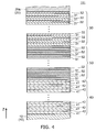
- FIG. 4 is a schematic cross-sectional view illustrating part of the configuration of another semiconductor light emitting device according to the embodiment of the invention.
- another semiconductor light emitting device 111 has multiple third layers 51 provided in an n-side intermediate layer 50.
- the multiple third layers 51 are stacked with one another. In other words, the multiple third layers 51 are stacked along the Z-axis direction.
- the n-side intermediate layer 50 further includes fourth layers 52, each of which is provided between the multiple third layers 51.
- the fourth layer 52 contains an n-type impurity with a concentration higher than that of the n-type impurity contained in the third layer 51.
- the fourth layer 52 contains Al y2 Ga 1-y2 N (0 ⁇ y2 ⁇ 0.01), where the Al composition ratio y2 in the fourth layer 52 may be the same as or different from the Al composition ratio y1 in the third layer 51.
- the Al composition ratio y2 is set to be larger than 0 and equal to or smaller than 0.01. When the Al composition ratio y2 is larger than 0.01, the crystallinity is prone to be deteriorated and, thus, the light emitting efficiency is prone to be deteriorated.
- the third layer 51 is a non-doped AlGaN layer and the fourth layer 52 is a Si-doped AlGaN layer.
- the thickness of the third layer 51 is approximately 1 nm and the thickness of the fourth layer 52 is approximately 1 nm.
- These third and fourth layers 51 and 52 are alternately stacked to make 25 stacked-layer pairs of the third and fourth layers 51 and 52 (50 layers in total).
- This stacked film may be used as the n-side intermediate layer 50.
- the third layers 51 and the fourth layers 52 are alternatively stacked to make 5 stacked-layer pairs (10 layers in total).
- This stacked film may be used as the n-side intermediate layer 50.
- a stacked structure of the third layers 51 and the fourth layers 52 is applied as the n-side intermediate layer 50, so that electronic carriers can be effectively injected. Accordingly, the stress in the semiconductor layers is relaxed without deteriorating the device characteristics. Consequently, a semiconductor light emitting device that operates at a lower operating voltage and achieves high light emitting efficiency can be provided.
- MOCVD Metal Organic Chemical Vapor Deposition
- MBE Molecular Beam Epitaxy
- TMG trimethyl gallium
- TMA trimethyl aluminum
- TMI trimethyl indium
- Cp 2 Mg bis(cyclopentadienyl)magnesium
- gas materials include ammonium (NH 3 ) and silane (SiH 4 ), and carrier gases include hydrogen and nitrogen.
- TMG trimethyl gallium
- TMG trimethyl aluminum
- TMI trimethyl indium
- SiH 4 Bis(cyclopentadienyl)magnesium
- carrier gases include hydrogen and nitrogen.
- TMG tri-ethyl gallium
- the substrate 5 uses a sapphire substrate, for example.
- the sapphire substrate is inclined by 0.2° with respect to a M-axis direction and includes a C-plane on which cylindrical concavity and convexity, each having a diameter of 3 ⁇ m, a height of 1 ⁇ m, and a pitch of 5 ⁇ m, are provided.
- the major surface of the substrate 5 facing the n-type semiconductor layer 10 may be inclined in the range from 0.1° to 0.5° with respect to the M-axis direction of the substrate 5.
- the crystallinity of various semiconductor layers to be grown on the substrate 5 is improved.
- an angle between the major surface of the substrate 5 and the M-axis direction is smaller than 0.1 °, the crystallinity is prone to be deteriorated.
- the angle is larger than 0.5°, the crystallinity is also prone to be deteriorated.
- the substrate 5 has concavity and convexity provided on the major surface. With these concavity and convexity, a path of the light emitted from the light emitting portion 30 can be changed, and, thus, light extraction efficiency is improve.
- the shapes (a planar shape when the concavity and convexity are cut so as to be parallel with the major surface of the substrate 5) of the concavity and convexity can be any shape.
- a semiconductor layer is grown on the substrate 5
- providing the concavity and convexity on the substrate 5 can cause the concavity and convexity to function as cores of the crystal growth, thereby bringing the effects of improving the crystallinity of the semiconductor layer.
- the substrate 5 is subject to, for example, an organic cleaning and an acid cleaning as a pretreatment. Thereafter, the substrate 5 is stored inside a MOCVD apparatus.
- the temperature of the substrate 5 is increased up to 1100°C by high-frequency heating in an atmosphere of a mixed gas of a nitride (N 2 ) gas and a hydrogen (H 2 ) gas under a normal pressure.
- a mixed gas of a nitride (N 2 ) gas and a hydrogen (H 2 ) gas under a normal pressure.
- the surface of the substrate 5 is subjected to a gas-phase etching and a natural oxide film which is formed on the surface is removed.
- the temperature of the substrate 5 is decreased down to 500°C and is kept at 500°C.
- an ammonium (NH 3 ) gas, TMG (Tri-Methyl Gallium), and TMA (Try-Methyl Aluminum) are supplied as process gases to form a buffer layer 6 containing AlGaN.
- the thickness of the buffer layer 6 is set to be, for example, 20 nm.
- the temperature of the substrate 5 is increased up to 1100°C and is kept at 1100°C.
- the base GaN layer 11 is an undoped layer.
- the thickness of the base GaN layer 11 is, for example, 3 ⁇ m.
- n-type contact layer 12 Thereafter, for example, silane (SiH 4 gas) to serve as an n-type dopant is supplied to form an n-type contact layer 12.
- the thickness of the n-type contact layer 12 is, for example, 4 ⁇ m.
- the n-type contact layer 12 is a GaN layer containing Si.
- the supply of TMG is stopped while the supply of the NH 3 gas is continued, and the temperature of the substrate 5 is decreased down to 800°C and is kept at 800°C.
- the first layer 41 is a Si-doped GaN layer.
- the thickness of the first layer 41 is set to be, for example, 2 nm.
- the second layer 42 is an InGaN layer with 0.1 of an In composition ratio (a second In composition ratio x2).
- the thickness of the second layer 42 is, for example, 1 nm
- n-side intermediate layer 50 is an undoped layer and is an AlGaN layer whose Al composition ratio y1 is 0.01.
- the thickness of the third layer 51 is, for example, 5 nm.
- the barrier layer 31 is a GaN layer.
- the thickness of the barrier layer 31 is, for example, 5 nm.
- TMI Tri-Methyl Indium
- the well layer 42 is, for example, an InGaN layer whose In composition ratio (the first In composition ratio x1) is 0.15.
- the thickness of the well layer 32 is, for example, 2.5 nm.
- the supply and stop of TMI is performed repeatedly, so that the barrier layer 31 and the well layer 32 are formed for 7 times, for example.
- the light emitting portion 30 having a multiple quantum well structure is obtained.
- the GaN cap layer 20a is, for example, an undoped GaN layer.
- the thickness of the GaN cap layer 20a is, for example, 5 nm.
- TMA Tri-Methyl Aluminum
- the AlGaN cap layer 20b is, for example, an undoped AlGaN layer whose Al composition ratio is 0.003.
- the thickness of the AlGaN cap layer 20b is, for example, 1 nm.
- the supplies of TMG and TMA are stopped, and the temperature of the substrate 5 is increased up to 1030°C in the N 2 gas atmosphere and is kept at 1030°C.
- the NH 3 gas, TMG, and TMA as process gases, and Bis(cyclopentadienyl)magnesium (Cp 2 Mg) as a p-type dopant are supplied, so that a p-type AlGaN layer 20c is formed.
- the Mg concentration of the p-type AlGaN layer 20c is, for example, 1x10 19 to 20 cm -3 .
- the thickness of the p-type AlGaN layer 20c is, for example, 10 nm.
- the p-type AlGaN layer 20c functions as an electronic barrier layer (an electronic overflow preventing layer).
- the Mg concentration of the p-type GaN clad laver 21 is, for example, 2x10 19 cm -3
- the thickness of the p-type GaN clad layer 21 is, for example, approximately 100 nm.
- the amount of supplying Cp 2 Mg is increased to form a p-type GaN contact layer 22.
- the Mg concentration of the p-type GaN contact layer 22 is, for example, 3x10 20 cm -3 .
- the thickness of the p-type GaN contact layer 22 is, for example, approximately 10 nm.
- the supply of TMG is stopped and only the carrier gas is continuously supplied, so that the temperature of the substrate 5 is naturally decreased.
- the supply of the NH 3 gas is continued until the temperature of the substrate 5 reaches 500°C.
- the substrate 5 is taken out from the MOCVD apparatus and part of the formed stacked structural body of the semiconductor layers is removed to reach the n-type contact layer 12 by, for example, a RIE (Reactive Ion Etching) method, so that part of the n-type contact layer 12 is exposed.
- a RIE Reactive Ion Etching
- an n-side electrode 71 formed of a Ti film/a Pt film/an Au film is formed on the exposed n-type contact layer 12.
- a p-side electrode 81 formed of, for example, a Ni film/an Au film is formed on the p-type GaN contact layer 22.
- the semiconductor light emitting device 110 illustrated in FIG. 1 is obtained.
- an operating voltage is 3.1 V (volt) to 3.5 V when a current is 20 mA, and a light output at this time is approximately 15 mW.
- the peak wavelength of light emission is approximately 450 nm.
- the stress caused in the semiconductor layers is relaxed in the semiconductor light emitting device 110 according to the embodiment.
- a semiconductor light emitting device that operates at a lower operating voltage and achieves high light emitting efficiency can be obtained.
- the semiconductor light emitting device 111 can be formed by stacking the multiple third layers 51 and the multiple fourth layers 52 in a process of forming the n-side intermediate layer 50.
- the multilayered structural body 40 is formed, and, thereafter, the third layers 51 containing undoped AlGaN whose Al composition ratio y1 is 0.01 are formed.
- the thickness of the third layer 51 is set to be, for example, 1 nm.
- the fourth layers 52 containing Si-doped AlGaN whose Al composition ratio y2 is 0.01 are formed.
- the thickness of the fourth layer 52 is set to be, for example, 1 nm.
- Those third and fourth layers 51 and 52 are formed in pair for 5 times (10 layers in total). As a result, the n-side intermediate layer 50 with a thickness of 10 nm is obtained, for example.
- the stress caused in the semiconductor slayers is relaxed in the semiconductor light emitting device 111 to be manufactured in this way.
- a semiconductor light emitting device that operates at a lower operating voltage and achieves high light emitting efficiency can be obtained.
- FIG. 5 is a graph illustrating characteristics of semiconductor light emitting devices.
- FIG. 5 shows changes of the light emitting characteristics when an In composition ratio in the multilayered structural body 40 of the semiconductor light emitting devices is changed.
- the horizontal axis represents a wavelength ⁇ (nm) and the vertical axis represents light emitting intensity lp.
- the light emitting intensity lp is standardized by setting the maximum intensity as 1.
- FIG. 5 illustrates characteristics of a semiconductor light emitting device in which no n-side intermediate layer 50 is provided. Also, FIG. 5 shows characteristics of two types of semiconductor light emitting devices 119a and 119b whose In composition ratios (second In composition ratio x2) are different from each other in the second layers 42 of the multilayered structural body 40.
- the second In composition ratio x2 is 0.14 in the semiconductor light emitting device 119a and the second In composition ratio x2 is 0.26 in the semiconductor light emitting device 119b.
- the wavelength width of the light emitting intensity lp is narrower than that of the semiconductor light emitting device 119a. Specifically, a half band width of the light emitting spectrum is reduced by 17.7 nm in the semiconductor light emitting device 119b as compared with that in the semiconductor light emitting device 119a.
- the operating voltage of the semiconductor light emitting device 119a is 3.5V to 3.6V, while the operating voltage of the semiconductor light emitting device 119b is 3.3V. In other words, the operating voltage decreases in a semiconductor light, emitting device whose second In composition ratio x2 of the second layer 42 is higher.
- the second In composition ratio x2 of the second layer 42 is increased, so that a preferable characteristic can be obtained.
- a growing temperature of the light emitting portion 30 is set to be higher than that of the multilayered structural body 40 in order to further improve the crystallinity of the light emitting portion 30.
- a growing temperature of the light emitting portion 30 is set to be higher than that of the multilayered structural body 40 in order to further improve the crystallinity of the light emitting portion 30.
- 800°C is employed as the growing temperature of the multilayered structural body 40
- 850°C is employed as the growing temperature of the light emitting portion 30.
- the temperature of growing the light emitting portion 30 after formation of the multilayered structural body 40 is set to be higher than the temperature of growing the multilayered structural body 40 in the comparative example where an n-side intermediate layer is not provided, In disappears in the second layers 42 which are formed by setting the In composition ratio to be higher. As a result, the second In composition ratio x2 may be lower than a desired value. In this case, desired characteristics cannot be obtained.
- an n-side intermediate layer 50 is provided, so that the n-side intermediate layer 50 functions as a cap layer of the multilayered structural body 40. Therefore, even when the temperature of growing the light emitting portion 30 is set to be higher than that of growing the multilayered structural body 40, the disappearance of In can be suppressed in the second layers 42. As a result, a desired second In composition ratio x2 is obtained, and, thus, desired characteristics can be obtained.
- the n-side intermediate layer 50 can achieve a function as a cap layer of the multilayered structural body 40 in addition to a function as a stress relaxation layer to suppress the compression stress CF.
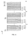
- FIG. 6 is a schematic cross-sectional view illustrating part of the configuration of another semiconductor light emitting device according to the embodiment of the invention.
- a semiconductor light emitting device 112 according to the embodiment further includes a p-side intermediate layer 60 in the semiconductor light emitting device 110 illustrated in FIG. 1 and FIG. 2 .
- the p-side intermediate layer 60 is provided between a light emitting portion 30 and a p-type semiconductor layer 20.
- the p-side intermediate layer 60 includes a fifth layer 61 containing Al z1 Ga 1-z1 N layer (0 ⁇ z1 ⁇ 0.01).
- the Al composition ratio z1 of the fifth layer 61 may be the same as or different from the Al composition ratio y1 of a third layer 51 and the Al composition ratio y2 of a fourth layer 52.
- the Al composition ratio z1 is set to be larger than 0 and equal to or smaller than 0.01.
- crystallinity is prone to be deteriorated.
- the light emitting efficiency is prone to be deteriorated.
- the p-side intermediate layer 60 is provided between the light emitting portion 30 and the p-type AlGaN layer 20c of the p-type semiconductor layer 20.
- the embodiment is not limited thereto. Similar to the semiconductor light emitting device 110 illustrated in FIG. 1 , the GaN cap layer 20a may be provided between the light emitting portion 30 and the p-type semiconductor layer 20, and the p-side intermediate layer 60 may be provided between the light emitting portion 30 and the GaN cap layer 20a. In this case, an AlGaN cap layer 20b may be further provided between the GaN cap layer 20a and the p-type semiconductor layer 20 (the p-type AlGaN layer 20c).
- the compressive stress to be accumulated in the stacked semiconductor layers can be further suppressed by the p-side intermediate layer 60 and the stress in the semiconductor layers is further relaxed.
- a semiconductor light emitting device that operates at a lower operating voltage and achieves high light emitting efficiency can be obtained.
- FIG. 7 is a schematic cross-sectional view illustrating part of the configuration of another semiconductor light emitting device according to the embodiment of the invention.
- multiple fifth layers 61 are provided in a semiconductor light emitting device 112a according to the embodiment.
- the multiple fifth layers 61 are stacked with one another. In other words, the multiple fifth layers 61 are stacked along the Z-axis direction.
- the p-side intermediate layer 60 further includes sixth layers 62, each of which is provided between the fifth layers 61.
- the sixth layer 62 contains a p-type impurity whose concentration is higher than that of the p-type impurity contained in the fifth layer 61.
- the sixth layer 62 contains Al z2 Ga 1-z2 N (0 ⁇ z2 ⁇ 0.01).
- the Al composition rate z2 in the sixth layer 62 may be the same as or different from the Al composition ratio z1 in the fifth layer 61.
- the Al composition ratio z2 in the sixth layer 62 may be the same as or different from the Al composition ratio y1 of the third layer 51 and the Al composition ratio y2 of the fourth layer 52.
- the Al composition ratio z2 is set to be larger than 0 and equal to or smaller than 0.01.
- the Al composition ratio z2 is larger than 0.01, the crystallinity is prone to be deteriorated. As a result, the light emitting efficiency is prone to be deteriorated.
- the fifth layer 61 is a non-doped AlGaN layer and the sixth layer 62 is an Mg-doped AlGaN layer.
- a multilayered structural body may be applied to the p-side intermediate layer 60. With this configuration, stress caused in semiconductor layers is relaxed. Thus, a semiconductor light emitting device that operates at a lower operating voltage and achieves high light emitting efficiency can be obtained.
- FIG. 8 is a schematic cross-sectional view illustrating part of the configuration of another semiconductor light emitting device according to the embodiment of the invention.
- another semiconductor light emitting device 112b has an n-side intermediate layer 50 with a multilayered structural body (multiple third layers 51 and multiple fourth layers 52) and a p-side intermediate layer 60 with a multilayered structural body (multiple fifth layers 61 and multiple sixth layers 62).
- the stress caused in the semiconductor layers is also relaxed in the semiconductor light emitting device 112b.
- a semiconductor light emitting device that operates at a lower operating voltage and achieves high light emitting efficiency can be obtained.
- an n-side intermediate layer 50 is provided between a multilayered structural body 40 and a light emitting portion 30.
- the n-side intermediate layer 50 is a single undoped AlGaN layer or a multilayer film in which an undoped AlGaN layer and a Si-doped GaN layer are stacked.
- This n-side intermediate layer 50 has a function to relax the stress, so that the compressive stress caused in the multilayered structural body 40 and the light emitting portion 30 having InGaN layer is relaxed. Accordingly, the defects to be generated in the stacked interface and the distortions to be caused in the well layer 32 can be reduced. Thus, a semiconductor light emitting device that achieves sufficient light output and operates at a lower operating voltage can be obtained.
- the description is given above by using the case where a C-plane sapphire substrate is used as the substrate 5.
- another substrate such as a GaN, SiC, or ZnO substrate may be used.
- the plane direction of the substrate 5 is not limited to the C-plane, and another plane, for example, a non-polar plane may be used.
- nitride semiconductors are intended to include semiconductors with all the compositions which are obtained by changing each of composition ratios x, y, and z in the respective ranges in the chemical formula: B x lnyAl z Ga 1-x-y-z N (0 ⁇ x ⁇ 1, 0 ⁇ y ⁇ 1, 0 ⁇ z ⁇ 1, x+y+z ⁇ 1). Furthermore, in the above chemical formula, the "nitride semiconductors” are intended to include ones further containing the V group elements other than N (nitride), ones further containing various elements which are to be added to control various properties such as conductivity types, and ones further containing various elements which are contained unintentionally.
- exemplary embodiments of the invention are described with reference to specific examples. However, the invention is not limited to these specific examples. For example, various modifications made by one skilled in the art in regard to the configurations, sizes, material qualities, arrangements, etc., of components of semiconductor light emitting devices such as n-type semiconductor layers, p-type semiconductor layers, light emitting portions, well layers, barrier layers, multilayered structural bodies, n-side intermediate layers, p-side intermediate layers, first to sixth layers, electrodes, substrates, and buffer layers are included in the scope of the invention to the extent that the purport of the invention is included.
- semiconductor light emitting devices such as n-type semiconductor layers, p-type semiconductor layers, light emitting portions, well layers, barrier layers, multilayered structural bodies, n-side intermediate layers, p-side intermediate layers, first to sixth layers, electrodes, substrates, and buffer layers are included in the scope of the invention to the extent that the purport of the invention is included.
Landscapes
- Chemical & Material Sciences (AREA)
- Engineering & Computer Science (AREA)
- Nanotechnology (AREA)
- Physics & Mathematics (AREA)
- Life Sciences & Earth Sciences (AREA)
- Biophysics (AREA)
- Optics & Photonics (AREA)
- Crystallography & Structural Chemistry (AREA)
- Led Devices (AREA)
Applications Claiming Priority (1)
| Application Number | Priority Date | Filing Date | Title |
|---|---|---|---|
| JP2010029516A JP5306254B2 (ja) | 2010-02-12 | 2010-02-12 | 半導体発光素子 |
Publications (2)
| Publication Number | Publication Date |
|---|---|
| EP2360745A2 true EP2360745A2 (de) | 2011-08-24 |
| EP2360745A3 EP2360745A3 (de) | 2012-07-25 |
Family
ID=44022913
Family Applications (1)
| Application Number | Title | Priority Date | Filing Date |
|---|---|---|---|
| EP10251557A Withdrawn EP2360745A3 (de) | 2010-02-12 | 2010-09-06 | Lichtemittierendes Halbleiterbauelement |
Country Status (6)
| Country | Link |
|---|---|
| US (1) | US8525195B2 (de) |
| EP (1) | EP2360745A3 (de) |
| JP (1) | JP5306254B2 (de) |
| KR (2) | KR101174574B1 (de) |
| CN (1) | CN102157648B (de) |
| TW (1) | TWI478383B (de) |
Cited By (2)
| Publication number | Priority date | Publication date | Assignee | Title |
|---|---|---|---|---|
| EP2802019A1 (de) * | 2013-05-06 | 2014-11-12 | LG Innotek Co., Ltd. | Lichtemittierende Vorrichtung |
| DE102016120419B4 (de) * | 2016-10-26 | 2025-12-31 | OSRAM Opto Semiconductors Gesellschaft mit beschränkter Haftung | Halbleiterkörper |
Families Citing this family (24)
| Publication number | Priority date | Publication date | Assignee | Title |
|---|---|---|---|---|
| US20130228743A1 (en) | 2012-03-01 | 2013-09-05 | Industrial Technology Research Institute | Light emitting diode |
| TWI499081B (zh) * | 2012-10-12 | 2015-09-01 | Ind Tech Res Inst | 發光二極體 |
| JP6026116B2 (ja) * | 2012-03-09 | 2016-11-16 | シャープ株式会社 | 窒化物半導体発光素子およびその製造方法 |
| CN102738333B (zh) * | 2012-04-16 | 2013-07-10 | 江苏汉莱科技有限公司 | 一种绿光发光二极管及其制备方法 |
| DE102012104671B4 (de) | 2012-05-30 | 2020-03-05 | Osram Opto Semiconductors Gmbh | Verfahren zur Herstellung einer aktiven Zone für einen optoelektronischen Halbleiterchip |
| KR101387543B1 (ko) * | 2012-08-21 | 2014-04-21 | 엘지전자 주식회사 | 질화물 반도체 발광 소자 |
| JP2012256948A (ja) * | 2012-09-28 | 2012-12-27 | Toshiba Corp | 半導体発光素子 |
| JP5460831B1 (ja) | 2012-11-22 | 2014-04-02 | 株式会社東芝 | 半導体発光素子 |
| JP6001446B2 (ja) * | 2012-12-28 | 2016-10-05 | 株式会社東芝 | 半導体発光素子及びその製造方法 |
| CN103187497B (zh) * | 2013-01-28 | 2015-11-25 | 上海博恩世通光电股份有限公司 | 一种提高大尺寸芯片光效的外延结构及其生长方法 |
| CN104134729B (zh) * | 2013-05-03 | 2017-04-26 | 展晶科技(深圳)有限公司 | 发光芯片及其制造方法 |
| KR102109048B1 (ko) * | 2013-05-14 | 2020-05-11 | 엘지이노텍 주식회사 | 반도체 기판, 발광 소자 및 전자 소자 |
| CN103413877B (zh) * | 2013-08-16 | 2016-01-20 | 湘能华磊光电股份有限公司 | 外延结构量子阱应力释放层的生长方法及其外延结构 |
| JP6183060B2 (ja) * | 2013-08-24 | 2017-08-23 | 日亜化学工業株式会社 | 半導体発光素子 |
| KR102109109B1 (ko) * | 2013-12-05 | 2020-05-12 | 엘지이노텍 주식회사 | 발광소자 및 조명시스템 |
| CN103872197B (zh) * | 2014-03-20 | 2017-07-11 | 西安神光皓瑞光电科技有限公司 | 一种提升GaN基LED芯片抗静电能力的外延生长方法 |
| CN104064644B (zh) * | 2014-06-30 | 2016-08-31 | 湘能华磊光电股份有限公司 | Led的量子阱结构、其制作方法及包括其的led外延片 |
| CN104701432A (zh) * | 2015-03-20 | 2015-06-10 | 映瑞光电科技(上海)有限公司 | GaN 基LED 外延结构及其制备方法 |
| KR102416010B1 (ko) * | 2015-03-31 | 2022-07-05 | 서울바이오시스 주식회사 | 자외선 발광 소자 |
| US10818818B2 (en) * | 2017-11-30 | 2020-10-27 | Epistar Corporation | Semiconductor device |
| CN109950375B (zh) * | 2019-01-31 | 2021-04-02 | 华灿光电(浙江)有限公司 | 发光二极管外延片及其生长方法 |
| US11843075B2 (en) * | 2020-09-11 | 2023-12-12 | Nichia Corporation | Nitride semiconductor element and method of manufacturing nitride semiconductor element |
| JP7154266B2 (ja) * | 2020-10-16 | 2022-10-17 | 日機装株式会社 | 窒化物半導体発光素子 |
| JP7714412B2 (ja) * | 2021-09-08 | 2025-07-29 | 日亜化学工業株式会社 | 発光素子 |
Citations (6)
| Publication number | Priority date | Publication date | Assignee | Title |
|---|---|---|---|---|
| EP1018770A1 (de) | 1997-08-20 | 2000-07-12 | Sanyo Electric Co., Ltd. | Halbleitervorrichtung auf basis einer galliumnitrid halbleiterverbindung |
| WO2002097904A2 (en) | 2001-05-30 | 2002-12-05 | Cree, Inc. | Group iii nitride based light emitting diode structures with a quantum well and superlattice |
| JP3427265B2 (ja) | 1998-12-08 | 2003-07-14 | 日亜化学工業株式会社 | 窒化物半導体素子 |
| WO2006022496A1 (en) | 2004-08-26 | 2006-03-02 | Lg Innotek Co., Ltd | Nitride semiconductor light emitting device and fabrication method thereof |
| EP1727212A1 (de) | 2004-03-19 | 2006-11-29 | Matsushita Electric Industrial Co., Ltd. | Halbleiter-lichtemissionsbauelement und beleuchtungseinrichtung |
| US20080251781A1 (en) * | 2007-04-16 | 2008-10-16 | Samsung Electro-Mechanics Co., Ltd. | Nitride semiconductor light emitting device |
Family Cites Families (5)
| Publication number | Priority date | Publication date | Assignee | Title |
|---|---|---|---|---|
| JPH10321942A (ja) * | 1997-05-14 | 1998-12-04 | Matsushita Electric Ind Co Ltd | 半導体発光素子 |
| CA2322490C (en) | 1998-03-12 | 2010-10-26 | Nichia Chemical Industries, Ltd. | Nitride semiconductor device |
| US6153894A (en) * | 1998-11-12 | 2000-11-28 | Showa Denko Kabushiki Kaisha | Group-III nitride semiconductor light-emitting device |
| JP2001036196A (ja) * | 2000-01-01 | 2001-02-09 | Nec Corp | p型ドーパント材料拡散防止層付き窒化ガリウム系発光素子 |
| CN100521260C (zh) * | 2002-07-16 | 2009-07-29 | 氮化物半导体株式会社 | 氮化镓类化合物半导体装置 |
-
2010
- 2010-02-12 JP JP2010029516A patent/JP5306254B2/ja active Active
- 2010-09-01 TW TW099129502A patent/TWI478383B/zh not_active IP Right Cessation
- 2010-09-01 US US12/873,662 patent/US8525195B2/en active Active
- 2010-09-06 EP EP10251557A patent/EP2360745A3/de not_active Withdrawn
- 2010-09-07 KR KR1020100087420A patent/KR101174574B1/ko not_active Expired - Fee Related
- 2010-09-08 CN CN2010102755667A patent/CN102157648B/zh not_active Expired - Fee Related
-
2012
- 2012-06-15 KR KR1020120064300A patent/KR101252414B1/ko not_active Expired - Fee Related
Patent Citations (6)
| Publication number | Priority date | Publication date | Assignee | Title |
|---|---|---|---|---|
| EP1018770A1 (de) | 1997-08-20 | 2000-07-12 | Sanyo Electric Co., Ltd. | Halbleitervorrichtung auf basis einer galliumnitrid halbleiterverbindung |
| JP3427265B2 (ja) | 1998-12-08 | 2003-07-14 | 日亜化学工業株式会社 | 窒化物半導体素子 |
| WO2002097904A2 (en) | 2001-05-30 | 2002-12-05 | Cree, Inc. | Group iii nitride based light emitting diode structures with a quantum well and superlattice |
| EP1727212A1 (de) | 2004-03-19 | 2006-11-29 | Matsushita Electric Industrial Co., Ltd. | Halbleiter-lichtemissionsbauelement und beleuchtungseinrichtung |
| WO2006022496A1 (en) | 2004-08-26 | 2006-03-02 | Lg Innotek Co., Ltd | Nitride semiconductor light emitting device and fabrication method thereof |
| US20080251781A1 (en) * | 2007-04-16 | 2008-10-16 | Samsung Electro-Mechanics Co., Ltd. | Nitride semiconductor light emitting device |
Cited By (5)
| Publication number | Priority date | Publication date | Assignee | Title |
|---|---|---|---|---|
| EP2802019A1 (de) * | 2013-05-06 | 2014-11-12 | LG Innotek Co., Ltd. | Lichtemittierende Vorrichtung |
| KR20140131770A (ko) * | 2013-05-06 | 2014-11-14 | 엘지이노텍 주식회사 | 반도체 기판, 발광 소자 및 전자 소자 |
| US9196791B2 (en) | 2013-05-06 | 2015-11-24 | Lg Innotek Co., Ltd. | Light emitting device |
| KR102075543B1 (ko) | 2013-05-06 | 2020-02-11 | 엘지이노텍 주식회사 | 반도체 기판, 발광 소자 및 전자 소자 |
| DE102016120419B4 (de) * | 2016-10-26 | 2025-12-31 | OSRAM Opto Semiconductors Gesellschaft mit beschränkter Haftung | Halbleiterkörper |
Also Published As
| Publication number | Publication date |
|---|---|
| CN102157648A (zh) | 2011-08-17 |
| TWI478383B (zh) | 2015-03-21 |
| US20110198583A1 (en) | 2011-08-18 |
| JP2011166031A (ja) | 2011-08-25 |
| TW201130157A (en) | 2011-09-01 |
| EP2360745A3 (de) | 2012-07-25 |
| KR20120080559A (ko) | 2012-07-17 |
| KR101252414B1 (ko) | 2013-04-08 |
| US8525195B2 (en) | 2013-09-03 |
| KR101174574B1 (ko) | 2012-08-16 |
| CN102157648B (zh) | 2013-07-10 |
| JP5306254B2 (ja) | 2013-10-02 |
| KR20110093568A (ko) | 2011-08-18 |
Similar Documents
| Publication | Publication Date | Title |
|---|---|---|
| US8525195B2 (en) | Semiconductor light emitting device | |
| US9331234B2 (en) | Semiconductor light emitting device and method for manufacturing semiconductor light emitting device | |
| CN109980057B (zh) | 第iii族氮化物半导体发光元件和其制造方法 | |
| US9166102B2 (en) | Group III nitride semiconductor light-emitting device including a superlatice layer | |
| US8227789B2 (en) | Optical semiconductor device and method of manufacturing the same | |
| JP5060656B2 (ja) | 窒化物半導体発光素子およびその製造方法 | |
| US9196786B2 (en) | Semiconductor light emitting element and method for manufacturing the same | |
| JP5861947B2 (ja) | 半導体発光素子及びその製造方法 | |
| US20120286237A1 (en) | Semiconductor light emitting device and wafer | |
| JP2008288397A (ja) | 半導体発光装置 | |
| JP6128138B2 (ja) | 半導体発光素子 | |
| CN103003964A (zh) | 氮化镓类化合物半导体发光元件和具有该发光元件的光源 | |
| EP2693499A1 (de) | Lichtemittierendes Gerät auf Halbleiterbasis und sein Herstellungsverfahren | |
| JP2008028121A (ja) | 半導体発光素子の製造方法 | |
| JP2012256948A (ja) | 半導体発光素子 | |
| US20220310874A1 (en) | Group iii nitride semiconductor device and method for producing same | |
| US10038118B2 (en) | Light emitting element | |
| JP2025041822A (ja) | 窒化物半導体発光素子 | |
| WO2016088732A1 (ja) | 半導体発光素子 |
Legal Events
| Date | Code | Title | Description |
|---|---|---|---|
| PUAI | Public reference made under article 153(3) epc to a published international application that has entered the european phase |
Free format text: ORIGINAL CODE: 0009012 |
|
| PUAI | Public reference made under article 153(3) epc to a published international application that has entered the european phase |
Free format text: ORIGINAL CODE: 0009012 |
|
| 17P | Request for examination filed |
Effective date: 20101004 |
|
| AK | Designated contracting states |
Kind code of ref document: A2 Designated state(s): AL AT BE BG CH CY CZ DE DK EE ES FI FR GB GR HR HU IE IS IT LI LT LU LV MC MK MT NL NO PL PT RO SE SI SK SM TR |
|
| AX | Request for extension of the european patent |
Extension state: BA ME RS |
|
| PUAL | Search report despatched |
Free format text: ORIGINAL CODE: 0009013 |
|
| AK | Designated contracting states |
Kind code of ref document: A3 Designated state(s): AL AT BE BG CH CY CZ DE DK EE ES FI FR GB GR HR HU IE IS IT LI LT LU LV MC MK MT NL NO PL PT RO SE SI SK SM TR |
|
| AX | Request for extension of the european patent |
Extension state: BA ME RS |
|
| RIC1 | Information provided on ipc code assigned before grant |
Ipc: H01L 33/02 20100101AFI20120620BHEP Ipc: H01S 5/02 20060101ALI20120620BHEP Ipc: H01L 33/32 20100101ALN20120620BHEP Ipc: H01L 33/12 20100101ALN20120620BHEP |
|
| 17Q | First examination report despatched |
Effective date: 20130402 |
|
| STAA | Information on the status of an ep patent application or granted ep patent |
Free format text: STATUS: THE APPLICATION IS DEEMED TO BE WITHDRAWN |
|
| 18D | Application deemed to be withdrawn |
Effective date: 20160121 |